EP0055073A1 - Improvements in or relating to electronic clock generators - Google Patents
Improvements in or relating to electronic clock generators Download PDFInfo
- Publication number
- EP0055073A1 EP0055073A1 EP81305906A EP81305906A EP0055073A1 EP 0055073 A1 EP0055073 A1 EP 0055073A1 EP 81305906 A EP81305906 A EP 81305906A EP 81305906 A EP81305906 A EP 81305906A EP 0055073 A1 EP0055073 A1 EP 0055073A1
- Authority
- EP
- European Patent Office
- Prior art keywords
- gate
- output
- transition
- clock
- stage
- Prior art date
- Legal status (The legal status is an assumption and is not a legal conclusion. Google has not performed a legal analysis and makes no representation as to the accuracy of the status listed.)
- Granted
Links
Images

Classifications
-
- H—ELECTRICITY
- H03—ELECTRONIC CIRCUITRY
- H03K—PULSE TECHNIQUE
- H03K5/00—Manipulating of pulses not covered by one of the other main groups of this subclass
- H03K5/15—Arrangements in which pulses are delivered at different times at several outputs, i.e. pulse distributors
- H03K5/151—Arrangements in which pulses are delivered at different times at several outputs, i.e. pulse distributors with two complementary outputs
- H03K5/1515—Arrangements in which pulses are delivered at different times at several outputs, i.e. pulse distributors with two complementary outputs non-overlapping
Definitions
- This invention relates to electronic clock generators.
- the invention relates to a clock generator with a two phase output.
- An object of the invention is to provide a relatively simple two phase clock generator in which the two output phases are effectively non-overlapping.
- a clock generator having a two phase output comprising a bistable circuit having two stages in which the output of each stage is cross coupled to one input of the other stage, each stage having a second input one of which is arranged to receive a clock signal, the other of which is arranged to receive the inverse of the clock signal, and wherein each cross coupling path includes an RC delay element which is so arranged that at a transition of said clock signals the output of one of said stages completes its transition substantially at the same time as the output of the other stage begins its transition.
- the RC elements are arranged so that they are effective on alternate clock transitions, only one being effective at any given transition.
- Each stage of the bistable circuit may comprise a pair of NOR gates.
- Each NOR gate may comprise a pair of MOS transistors with a common load transistor.
- Each cross coupling path may include a high resistance transfer MOS transistor which provides the resistance of the RC element, the capacitance being provided by the gate of one of the MOS transistors of the NOR gate.
- a feature of the present invention is that one of said load transistors may be arranged to be driven by the clock signal and the other by the inverse of the clock signal.
- the present invention is particularly suitable for fabrication in MOS 5V N-channel technology.
- a two phase clock generator comprises a basic bistable circuit formed from a pair of NOR gates 10 and 11.
- the NOR gate 10 comprises a pair of MOS transistors 12, 14 which have a common load transistor 15 and the NOR gate 11 comprises a pair of MOS transistors 15, 16 which have a common load transistor 17.
- the output from the NOR gate 10 is coupled to an input gate of the NOR gate 11 by way of a high resistance transfer MOS transistor 18 and the output from the NOR gate 11 is coupled to an input gate of the NOR gate 10 by way of a high resistance transfer MOS transistor 20.
- the gates of the MOS transistors 18 and 20 are each connected to supply line V which is set at +5 volts.
- the cross coupling paths of the bistable circuit each include an RC element in which the resistance is provided by the MOS transistor 18, 20 and the capacitance is provided by the gate of the MOS transistor 14, 15 of the NOR gate.
- the other input 19 to the NOR gate 10 is from a source of clock signals by way of a line 22 and the other input 21 to the NOR gate 11 is the inverted clock signal, the inversion being carried out by a transistor 25.
- the gate of the load transistor 17 is connected to receive the clock signal and the gate of the transistor 15 is connected to receive the inverted clock signal.
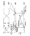
- Figure 2(a) shows the clock signal on line 22 (waveform 28) and the inverted clock signal (waveform 29) applied to one input of the NOR gate 11.
- the node shown at D in Figure 1 is at logic 1 and the node B of the NOR gate 15 is at logic 0 since the inverted clock signal is high.
- the transistor 12 is constructed so that when the clock signal 28 switches from a low to a high condition as represented by the transition 30, the node D discharges to a low condition in a relatively short time as represented by the transition 31 ( Figure 2(b) ).
- the transistor 18 has a relatively high resistance so that the capacitance of the gate of the transistor 15 is slow to discharge as represented by the line 32 ( Figure 2(b) ). It will be noted that initially this gate is charged to a voltage of V - V TH where V TH is a typical threshold voltage for MOS logic. This means that after the gate of transistor 16 goes low due to the transition of the inverted clock signal the potential at the node B does not commence to rise appreciably because of the slow discharge of the gate of the transistor 15.
- CR is made equal to fx t o nsecs where f is appropriately chosen to provide a delay which is such that ideally the node B begins to rise at about the same time the node D has settled to logic 0 (see waveform diagrams 2b and 2c). There is a small degree of overlap represented by shaded area 36 but this occurs at a voltage which is well below the nominal threshold voltage V TH of any logic circuits. Thereafter the node B rises rapidly under the dynamic pull of its associated load MOS transistor as shown by the transition 37 ( Figure 2(c) ).
- circuit of Figure 1 produces a two phase clock signal in which the two phases are effectively non-overlapping.
- the generator is particularly suitable for driving low capacitive loads of say less than approximately 5 pf and can be implemented in MOS 5V N-channel technology.
- the high resistance gates 18 and 20 are enhancement-type transistors. It will be appreciated that other types of device could be used. For example the gates could be depletion type devices in which case the transistors 14 to the voltage V.
- FIG. 1 The arrangement shown in Figure 1 is for driving low capacitive loads of typically 5 pf or less.
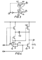
- An arrangement which can drive loads of up to 30 pf is shown in Figures 3 and 4.
- Figure 3 shows schematically the basic bistable arrangement which comprises gate circuits 110 and 111 and produces an output having two phases ⁇ 1 and ⁇ 2 .
- Each gate circuit 110, 111 is shown in detail in Figure 4 and includes a pair of MOS transistors 112, 114 which operate in the manner described for transistors 12, 14 of Figure 1.
- Transistor 120 is a high resistance transistor corresponding to transistor 20 of Figure 1 to provide the RC element in the cross coupling path.
- the output from the other gate circuit of the bistable is received at terminal A1 and clock signals are fed to terminal A2.
- the output of the circuit shown in Figure 4 includes a push-pull arrangement comprising transistors 130 and 131. This arrangement gives the circuit the ability to drive the higher capacitance load.
- Capacitor 132 is a feedback capacitor to provide the necessary drive signals for the transistors.
Abstract
Description
- This invention relates to electronic clock generators. In particular the invention relates to a clock generator with a two phase output.
- There is a requirement in some electronic circuit applications for a two phase electronic clock generator in which the overlap between the two output phases of the generator can be controlled so that they are_effectively non-overlapping. * An object of the invention is to provide a relatively simple two phase clock generator in which the two output phases are effectively non-overlapping.
- According to the present invention there is provided a clock generator having a two phase output comprising a bistable circuit having two stages in which the output of each stage is cross coupled to one input of the other stage, each stage having a second input one of which is arranged to receive a clock signal, the other of which is arranged to receive the inverse of the clock signal, and wherein each cross coupling path includes an RC delay element which is so arranged that at a transition of said clock signals the output of one of said stages completes its transition substantially at the same time as the output of the other stage begins its transition. The RC elements are arranged so that they are effective on alternate clock transitions, only one being effective at any given transition. By appropriately selecting the delays provided by the RC elements it is possible to generate a two phase clock output in which the two phases are effectively non-overlapping.
- Each stage of the bistable circuit may comprise a pair of NOR gates. Each NOR gate may comprise a pair of MOS transistors with a common load transistor. Each cross coupling path may include a high resistance transfer MOS transistor which provides the resistance of the RC element, the capacitance being provided by the gate of one of the MOS transistors of the NOR gate.
- A feature of the present invention is that one of said load transistors may be arranged to be driven by the clock signal and the other by the inverse of the clock signal.
- The present invention is particularly suitable for fabrication in
MOS 5V N-channel technology. - The invention will be described now by way of example only with particular reference to the accompanying drawings. In the drawings:
- Figure 1 is a circuit diagram of a clock generator in accordance with the present invention,
- Figures 2(a) to 2(c) are waveform diagrams illustrating the waveforms at various points in the circuit of Figure 1, and
- Figures 3 and 4 illustrate another embodiment of a clock generator in accordance with the present invention.
- Referring to Figure 1 a two phase clock generator comprises a basic bistable circuit formed from a pair of
NOR gates gate 10 comprises a pair ofMOS transistors common load transistor 15 and theNOR gate 11 comprises a pair ofMOS transistors common load transistor 17. The output from theNOR gate 10 is coupled to an input gate of theNOR gate 11 by way of a high resistancetransfer MOS transistor 18 and the output from theNOR gate 11 is coupled to an input gate of theNOR gate 10 by way of a high resistancetransfer MOS transistor 20. The gates of theMOS transistors - It will thus be seen that the cross coupling paths of the bistable circuit each include an RC element in which the resistance is provided by the
MOS transistor MOS transistor - The
other input 19 to theNOR gate 10 is from a source of clock signals by way of aline 22 and theother input 21 to theNOR gate 11 is the inverted clock signal, the inversion being carried out by atransistor 25. It will be noted that the gate of theload transistor 17 is connected to receive the clock signal and the gate of thetransistor 15 is connected to receive the inverted clock signal. With this arrangement, +5 volts is produced on the gate of a load transistor for a logic 0 to 1 transition. This means that a faster edge.speed is obtained than in the case of a conventional arrangement of load transistor in which the gate and source are connected together. On the logic 1 to 0 transition, logic 0 volts is applied to the gate of the load transistor and the speed of the discharge for a given size of transistor is then dependent only on the size of the driver transistor. Overall the arrangement produces a fast edge speed with full logic swing and minimal power consumption. The output loads are represented by CL. - The operation of the circuit will be described now with reference.to Figure 2. Figure 2(a) shows the clock signal on line 22 (waveform 28) and the inverted clock signal (waveform 29) applied to one input of the
NOR gate 11. Considering the situation when theclock signal 28 is low, then the node shown at D in Figure 1 is at logic 1 and the node B of theNOR gate 15 is at logic 0 since the inverted clock signal is high. This means that the output represeated by ø2 is high and the output represented by ø1 is low. Thetransistor 12 is constructed so that when theclock signal 28 switches from a low to a high condition as represented by thetransition 30, the node D discharges to a low condition in a relatively short time as represented by the transition 31 (Figure 2(b) ). Now thetransistor 18 has a relatively high resistance so that the capacitance of the gate of thetransistor 15 is slow to discharge as represented by the line 32 (Figure 2(b) ). It will be noted that initially this gate is charged to a voltage of V - VTH where VTH is a typical threshold voltage for MOS logic. This means that after the gate oftransistor 16 goes low due to the transition of the inverted clock signal the potential at the node B does not commence to rise appreciably because of the slow discharge of the gate of thetransistor 15. If this condition exists for a period of to nsecs after the discharge of the node D, then CR is made equal to fx to nsecs where f is appropriately chosen to provide a delay which is such that ideally the node B begins to rise at about the same time the node D has settled to logic 0 (see waveform diagrams 2b and 2c). There is a small degree of overlap represented byshaded area 36 but this occurs at a voltage which is well below the nominal threshold voltage VTH of any logic circuits. Thereafter the node B rises rapidly under the dynamic pull of its associated load MOS transistor as shown by the transition 37 (Figure 2(c) ). - A similar sequence of events occur at the high to low transition of the clock signal. This is also illustrated in the waveforms of Figure 2. It will be seen that the potential at the node B falls rapidly as shown by
transition 38 by way of thetransistor 16 whilst because of the high resistance provided bytransistor 20 the capacitance of the gate of thetransistor 14 discharges only slowly as shown by thewaveform 39. The effect of this is that the potential at the node D does not start to rise until the potential at node B has reached the logic 0 level. There is a small area of overlap as represented by theshaded area 40 but again this is at a potential which is well below the threshold level. - Thus it will be see that the circuit of Figure 1 produces a two phase clock signal in which the two phases are effectively non-overlapping. The generator is particularly suitable for driving low capacitive loads of say less than approximately 5 pf and can be implemented in
MOS 5V N-channel technology. - As described the
high resistance gates transistors 14 to the voltage V. - The arrangement shown in Figure 1 is for driving low capacitive loads of typically 5 pf or less. An arrangement which can drive loads of up to 30 pf is shown in Figures 3 and 4. Figure 3 shows schematically the basic bistable arrangement which comprises
gate circuits gate circuit MOS transistors transistors Transistor 120 is a high resistance transistor corresponding totransistor 20 of Figure 1 to provide the RC element in the cross coupling path. The output from the other gate circuit of the bistable is received at terminal A1 and clock signals are fed to terminal A2. - It will be seen that the output of the circuit shown in Figure 4 includes a push-pull
arrangement comprising transistors
Claims (6)
Priority Applications (1)
| Application Number | Priority Date | Filing Date | Title |
|---|---|---|---|
| AT81305906T ATE14261T1 (en) | 1980-12-22 | 1981-12-16 | ELECTRONIC CLOCK SIGNAL GENERATORS. |
Applications Claiming Priority (2)
| Application Number | Priority Date | Filing Date | Title |
|---|---|---|---|
| GB8040979 | 1980-12-22 | ||
| GB8040979 | 1980-12-22 |
Publications (2)
| Publication Number | Publication Date |
|---|---|
| EP0055073A1 true EP0055073A1 (en) | 1982-06-30 |
| EP0055073B1 EP0055073B1 (en) | 1985-07-10 |
Family
ID=10518152
Family Applications (1)
| Application Number | Title | Priority Date | Filing Date |
|---|---|---|---|
| EP81305906A Expired EP0055073B1 (en) | 1980-12-22 | 1981-12-16 | Improvements in or relating to electronic clock generators |
Country Status (6)
| Country | Link |
|---|---|
| US (1) | US4472645A (en) |
| EP (1) | EP0055073B1 (en) |
| JP (1) | JPS57168518A (en) |
| AT (1) | ATE14261T1 (en) |
| CA (1) | CA1175917A (en) |
| DE (1) | DE3171351D1 (en) |
Cited By (3)
| Publication number | Priority date | Publication date | Assignee | Title |
|---|---|---|---|---|
| EP0424249A2 (en) * | 1989-10-16 | 1991-04-24 | Fujitsu Limited | A trigger pulse generating circuit |
| EP0463854A1 (en) * | 1990-06-25 | 1992-01-02 | Nec Corporation | Clocked driver circuit |
| DE19720017B4 (en) * | 1996-05-13 | 2004-06-03 | NEC Compound Semiconductor Devices, Ltd., Kawasaki | 90 ° phase shifter |
Families Citing this family (9)
| Publication number | Priority date | Publication date | Assignee | Title |
|---|---|---|---|---|
| US4625126A (en) * | 1984-06-29 | 1986-11-25 | Zilog, Inc. | Clock generator for providing non-overlapping clock signals |
| US4645947A (en) * | 1985-12-17 | 1987-02-24 | Intel Corporation | Clock driver circuit |
| US4694197A (en) * | 1986-01-06 | 1987-09-15 | Rca Corporation | Control signal generator |
| DE3685026D1 (en) * | 1986-07-09 | 1992-05-27 | Itt Ind Gmbh Deutsche | CLOCKED CMOS SWITCHING WITH AT LEAST ONE CMOS SWITCH. |
| EP0262412A1 (en) * | 1986-09-01 | 1988-04-06 | Siemens Aktiengesellschaft | Load-adapted CMOS clock generator |
| JPS63110811A (en) * | 1986-10-28 | 1988-05-16 | Mitsubishi Electric Corp | Clock generator |
| US5352937A (en) * | 1992-11-16 | 1994-10-04 | Rca Thomson Licensing Corporation | Differential comparator circuit |
| US5672991A (en) * | 1995-04-14 | 1997-09-30 | International Business Machines Corporation | Differential delay line circuit for outputting signal with equal pulse widths |
| JP4156075B2 (en) * | 1998-04-23 | 2008-09-24 | 株式会社半導体エネルギー研究所 | Image display device |
Citations (6)
| Publication number | Priority date | Publication date | Assignee | Title |
|---|---|---|---|---|
| US3292100A (en) * | 1966-01-04 | 1966-12-13 | Gen Electric | Pulse generator with multiple phasedisplaced outputs |
| DE1286101B (en) * | 1966-12-09 | 1969-01-02 | Sits Soc It Telecom Siemens | Device for distributing serial input pulses to parallel outputs |
| US3767945A (en) * | 1971-02-05 | 1973-10-23 | Siemens Ag | Circuit and construction of semiconductor storage elements |
| US3927334A (en) * | 1974-04-11 | 1975-12-16 | Electronic Arrays | MOSFET bistrap buffer |
| US3961269A (en) * | 1975-05-22 | 1976-06-01 | Teletype Corporation | Multiple phase clock generator |
| FR2339996A1 (en) * | 1976-01-31 | 1977-08-26 | Itt | INTEGRATED CLOCK PULSE CONFORMING CIRCUIT |
Family Cites Families (4)
| Publication number | Priority date | Publication date | Assignee | Title |
|---|---|---|---|---|
| US3578989A (en) * | 1969-06-17 | 1971-05-18 | Rca Corp | Pulse width stabilized monostable multivibrator |
| US3668436A (en) * | 1969-12-15 | 1972-06-06 | Computer Design Corp | Circuit apparatus for supplying first and second trains of mutually exclusive clock pulses |
| DE2837882C2 (en) * | 1978-08-30 | 1984-03-29 | Siemens AG, 1000 Berlin und 8000 München | Clock shaper for integrated semiconductor digital circuits |
| JPS5694654A (en) * | 1979-12-27 | 1981-07-31 | Toshiba Corp | Generating circuit for substrate bias voltage |
-
1981
- 1981-12-16 DE DE8181305906T patent/DE3171351D1/en not_active Expired
- 1981-12-16 EP EP81305906A patent/EP0055073B1/en not_active Expired
- 1981-12-16 AT AT81305906T patent/ATE14261T1/en not_active IP Right Cessation
- 1981-12-21 CA CA000392784A patent/CA1175917A/en not_active Expired
- 1981-12-21 JP JP56207972A patent/JPS57168518A/en active Pending
- 1981-12-22 US US06/333,435 patent/US4472645A/en not_active Expired - Fee Related
Patent Citations (6)
| Publication number | Priority date | Publication date | Assignee | Title |
|---|---|---|---|---|
| US3292100A (en) * | 1966-01-04 | 1966-12-13 | Gen Electric | Pulse generator with multiple phasedisplaced outputs |
| DE1286101B (en) * | 1966-12-09 | 1969-01-02 | Sits Soc It Telecom Siemens | Device for distributing serial input pulses to parallel outputs |
| US3767945A (en) * | 1971-02-05 | 1973-10-23 | Siemens Ag | Circuit and construction of semiconductor storage elements |
| US3927334A (en) * | 1974-04-11 | 1975-12-16 | Electronic Arrays | MOSFET bistrap buffer |
| US3961269A (en) * | 1975-05-22 | 1976-06-01 | Teletype Corporation | Multiple phase clock generator |
| FR2339996A1 (en) * | 1976-01-31 | 1977-08-26 | Itt | INTEGRATED CLOCK PULSE CONFORMING CIRCUIT |
Non-Patent Citations (1)
| Title |
|---|
| IBM Technical Disclosure Bulletin, Vol. 22, No. 3, August 1979 New York (US) B. CASSIDY et al.: "Dynamic Mosfet Logic Clock Driver" pages 1093-1094 * page 1093, last line to page 1094; figures 1,2 * * |
Cited By (4)
| Publication number | Priority date | Publication date | Assignee | Title |
|---|---|---|---|---|
| EP0424249A2 (en) * | 1989-10-16 | 1991-04-24 | Fujitsu Limited | A trigger pulse generating circuit |
| EP0424249A3 (en) * | 1989-10-16 | 1992-04-15 | Fujitsu Limited | A trigger pulse generating circuit |
| EP0463854A1 (en) * | 1990-06-25 | 1992-01-02 | Nec Corporation | Clocked driver circuit |
| DE19720017B4 (en) * | 1996-05-13 | 2004-06-03 | NEC Compound Semiconductor Devices, Ltd., Kawasaki | 90 ° phase shifter |
Also Published As
| Publication number | Publication date |
|---|---|
| JPS57168518A (en) | 1982-10-16 |
| ATE14261T1 (en) | 1985-07-15 |
| CA1175917A (en) | 1984-10-09 |
| DE3171351D1 (en) | 1985-08-14 |
| EP0055073B1 (en) | 1985-07-10 |
| US4472645A (en) | 1984-09-18 |
Similar Documents
| Publication | Publication Date | Title |
|---|---|---|
| US5896045A (en) | Static pulsed cross-coupled level shifter and method therefor | |
| KR900004590B1 (en) | Output buffer circuit | |
| US6064251A (en) | System and method for a low voltage charge pump with large output voltage range | |
| US4740717A (en) | Switching device with dynamic hysteresis | |
| EP0098060B1 (en) | Clock pulse generating circuit | |
| KR930008876B1 (en) | High voltage generating circuit of semicondcutor device | |
| US4063117A (en) | Circuit for increasing the output current in MOS transistors | |
| EP0606912B1 (en) | CMOS polyphase clock generation circuits | |
| EP0086090B1 (en) | Drive circuit for capacitive loads | |
| EP0055073A1 (en) | Improvements in or relating to electronic clock generators | |
| US4894559A (en) | Buffer circuit operable with reduced power consumption | |
| US4101788A (en) | Mos buffer circuit | |
| JP3698550B2 (en) | Boost circuit and semiconductor device using the same | |
| US4352996A (en) | IGFET Clock generator circuit employing MOS boatstrap capacitive drive | |
| US4468576A (en) | Inverter circuit having transistors operable in a shallow saturation region for avoiding fluctuation of electrical characteristics | |
| EP0468210B1 (en) | Circuit for driving a floating circuit in response to a digital signal | |
| US4611134A (en) | Bootstrap driving circuit | |
| JPH06296130A (en) | Data output circuit | |
| US6424173B1 (en) | Voltage translators with zero static power and predictable performance | |
| EP0109004B1 (en) | Low power clock generator | |
| KR100313512B1 (en) | Power on detect circuit | |
| JPH0351334B2 (en) | ||
| US6559678B1 (en) | Node predisposition circuit | |
| JP2765330B2 (en) | Output circuit | |
| EP0057025B1 (en) | Switching circuit |
Legal Events
| Date | Code | Title | Description |
|---|---|---|---|
| PUAI | Public reference made under article 153(3) epc to a published international application that has entered the european phase |
Free format text: ORIGINAL CODE: 0009012 |
|
| AK | Designated contracting states |
Designated state(s): AT BE CH DE FR GB IT NL SE |
|
| 17P | Request for examination filed |
Effective date: 19821020 |
|
| GRAA | (expected) grant |
Free format text: ORIGINAL CODE: 0009210 |
|
| AK | Designated contracting states |
Designated state(s): AT BE CH DE FR GB IT LI NL SE |
|
| PG25 | Lapsed in a contracting state [announced via postgrant information from national office to epo] |
Ref country code: NL Effective date: 19850710 Ref country code: LI Effective date: 19850710 Ref country code: IT Free format text: LAPSE BECAUSE OF FAILURE TO SUBMIT A TRANSLATION OF THE DESCRIPTION OR TO PAY THE FEE WITHIN THE PRESCRIBED TIME-LIMIT;WARNING: LAPSES OF ITALIAN PATENTS WITH EFFECTIVE DATE BEFORE 2007 MAY HAVE OCCURRED AT ANY TIME BEFORE 2007. THE CORRECT EFFECTIVE DATE MAY BE DIFFERENT FROM THE ONE RECORDED. Effective date: 19850710 Ref country code: FR Free format text: THE PATENT HAS BEEN ANNULLED BY A DECISION OF A NATIONAL AUTHORITY Effective date: 19850710 Ref country code: CH Effective date: 19850710 Ref country code: BE Effective date: 19850710 Ref country code: AT Effective date: 19850710 |
|
| REF | Corresponds to: |
Ref document number: 14261 Country of ref document: AT Date of ref document: 19850715 Kind code of ref document: T |
|
| PG25 | Lapsed in a contracting state [announced via postgrant information from national office to epo] |
Ref country code: SE Effective date: 19850730 |
|
| REF | Corresponds to: |
Ref document number: 3171351 Country of ref document: DE Date of ref document: 19850814 |
|
| REG | Reference to a national code |
Ref country code: CH Ref legal event code: PL |
|
| NLV1 | Nl: lapsed or annulled due to failure to fulfill the requirements of art. 29p and 29m of the patents act | ||
| EN | Fr: translation not filed | ||
| PLBE | No opposition filed within time limit |
Free format text: ORIGINAL CODE: 0009261 |
|
| STAA | Information on the status of an ep patent application or granted ep patent |
Free format text: STATUS: NO OPPOSITION FILED WITHIN TIME LIMIT |
|
| 26N | No opposition filed | ||
| PG25 | Lapsed in a contracting state [announced via postgrant information from national office to epo] |
Ref country code: DE Effective date: 19860902 |
|
| REG | Reference to a national code |
Ref country code: GB Ref legal event code: 732 |
|
| PGFP | Annual fee paid to national office [announced via postgrant information from national office to epo] |
Ref country code: GB Payment date: 19951121 Year of fee payment: 15 |
|
| PG25 | Lapsed in a contracting state [announced via postgrant information from national office to epo] |
Ref country code: GB Effective date: 19961216 |
|
| GBPC | Gb: european patent ceased through non-payment of renewal fee |
Effective date: 19961216 |