EP0057978A1 - High accuracy AC electric energy metering system - Google Patents
High accuracy AC electric energy metering system Download PDFInfo
- Publication number
- EP0057978A1 EP0057978A1 EP82300195A EP82300195A EP0057978A1 EP 0057978 A1 EP0057978 A1 EP 0057978A1 EP 82300195 A EP82300195 A EP 82300195A EP 82300195 A EP82300195 A EP 82300195A EP 0057978 A1 EP0057978 A1 EP 0057978A1
- Authority
- EP
- European Patent Office
- Prior art keywords
- signal
- sample
- reset
- gate
- responsive
- Prior art date
- Legal status (The legal status is an assumption and is not a legal conclusion. Google has not performed a legal analysis and makes no representation as to the accuracy of the status listed.)
- Ceased
Links
Images


Classifications
-
- G—PHYSICS
- G01—MEASURING; TESTING
- G01R—MEASURING ELECTRIC VARIABLES; MEASURING MAGNETIC VARIABLES
- G01R11/00—Electromechanical arrangements for measuring time integral of electric power or current, e.g. of consumption
-
- G—PHYSICS
- G01—MEASURING; TESTING
- G01R—MEASURING ELECTRIC VARIABLES; MEASURING MAGNETIC VARIABLES
- G01R21/00—Arrangements for measuring electric power or power factor
- G01R21/133—Arrangements for measuring electric power or power factor by using digital technique
-
- G—PHYSICS
- G01—MEASURING; TESTING
- G01R—MEASURING ELECTRIC VARIABLES; MEASURING MAGNETIC VARIABLES
- G01R21/00—Arrangements for measuring electric power or power factor
Definitions
- the present invention is related to electrical energy measuring devices for electric utility systems, and more particularly to solid state devices utilizing digital processing techniques.
- solid state electric energy metering systems are becoming increasingly more common. Nevertheless, substantial problems have to be overcome before solid state circuits can be applied to electric energy metering systems.
- One problem is due to the fact that solid state circuits operate utilizing low voltage input signals whereas the input signals available at the point of measurement for metering systems are line voltage and line current. Substantial problems are encountered in producing the requisite low level input signals from line voltage and line current.
- Another problem is that line current varies from approximately 1/2 to 200 amperes.
- devices such as microprocessors operate digitally.
- a digital processing and calculating AC electric energy measuring system is shown to include a sequence controller and a calculator subsystem for controlling the metering system operations in accordance with a predetermined program.
- An analog input circuit receives voltage and current signal components of an electric energy quantity to be measured by the metering system.
- a sample timer circuit utilizes the sequence controller and calculator subsystem clock for producing sample interval timer pulses which initiate each randomized sampling interval. Instantaneous sample values of the voltage and current signals are thus obtained at randomized sampling times in response to the sample timer interval pulses. The instantaneous signal values are sequentially digitized by a analog-to-digital converter.
- a plurality of parameters of the electric energy quantity to be measured are calculated in a common calculation program subroutine operating on the digitized instantaneous signal values. Totalizing each of these calculated values produces the value of the time integral of the measured electric energy parameter.
- An output readout or display produces numerical readings representative of the plurality of electric energy parameters calculated by the metering system.
- a plurality of output pulse data signals representing the calculated parameters are input to a pulse receiver device c.apable of transmitting the data pulses through a remote metering telemetry system or for being recorded in a recorder type of receiver device.
- the chief object of the present invention is to provide an AC electric energy metering system which overcomes past problems and provides substantial improvements in the accuracy and reliability of the system.
- an AC electric energy metering system for calculating a plurality of indicia of an AC electric energy quantity delivered by an electric utility system
- said metering system comprising signal sample means including inputs and outputs, said inputs receiving line voltages and currents determining the magnitude of the AC electric energy quantity, said outputs producing sample values representative of the instantaneous magnitudes of said line voltages and currents when said signal sample means is rendered to a sampling state; sample timer means producing a sample signal having first and second states, said first state occurring at randomly varying intervals and rendering said signal sample means to said sampling state at randomly occurring sampling times; analog-to-digital converter means producing binary signal representations of each of said sample values; control means calculating the plurality of indicia of said AC electric energy quantity from said binary signal representations of each of said sample values, said control means producing a reset interval signal composed of pulses, said pulses resetting said sample timer means; means resetting said control means when a pulse of said reset interval signal is input to
- the present disclosure reveals a high accuracy AC electric energy metering system capable of calculating a plurality of indicia of an AC electric energy quantity delivered to a load.
- indicia include real power measured in kilowatts, reactive power measured in var's and volts squared as well as the time integral of these quantities.
- the present invention utilizes an input module which produces six analog input signals representative of the voltages and currents in a three phase power distribution system.
- the six analog input signals are input to a sample and hold circuit which produces sample values representative of the instantaneous magnitude of each of the six input signals.
- the sample values representative of the instantaneous magnitude of the three phase voltages are input directly to a multiplexer.
- the sample values representative of the instantaneous magnitude of the three phase currents are input both directly to the multiplexer and to the multiplexer through ranging amplifiers.
- the ranging amplifiers are used to amplify the sample values of the three phase currents. This amplification results in significant improvement in the accuracy of the electric energy metering system and is considered to be an important improvement.
- the sample values of the three phase voltages and currents are sequentially input to an analog-to-digital converter.
- the digitized sample values are input to a control circuit wherein the desired quantities are calculated.
- the results of the calculation are input to an output module which produces appropriate visual readings.
- the output module may additionally act as an interface for a recording device or a remote meter reading system.
- a timing circuit is used to time out sampling intervals. At that end of each sampling interval the control circuit instructs the sample and hold circuit to produce new sample values. The control circuit then resets the timing circuit. A timing window is produced within the timing circuit which determines the appropriate times during which the control circuit should reset the timing circuit. If the control circuit attempts to reset the timing circuit outside of the timing window, it is presumed that the control circuit is lost and the timing circuit resets the control circuit. Additional failure modes of the control circuit are detected by a failure of the control circuit to reset the timing circuit or if the control circuit produces a reset signal of inappropriate duration. In either case the timing circuit will initiate a reset of the control circuit. The timing circuit greatly improves the reliability of the electric energy metering system disclosed herein.
- FIG. 1 a solid state AC electric energy metering system 10 constructed according to the teachings of the present invention is shown.
- the metering system 10 shown in Figure 1 is similar in design and operation to the metering system shown in U.K. Letters Patent 1578174 which is assigned to the same assignee as the present invention.
- U.K. Patent should be consulted for further circuit details and elements not considered to be important features of the present invention as well as a detailed description of the operation of the metering system 10.
- an input module 12 produces voltage component signals V A , V B and V c and current component signals I A , I B and I c representative of a three phase AC electric energy quantity delivered to a load (not shown) by a power distribution system consisting of conductors 7, 8 and 9.
- the voltage component signals V A , V B and V c are produced by conventional potential transformers (not shown) and are representative of the three phase voltages A, B and C, respectively.
- the current component signals I A , I B and I C are produced by conventional current transformers (not shown) and are representative of the three phase currents A, B and C, respectively.
- the voltage component signals and the current component signals are input to a sample and hold circuit 14.
- the sample and hold circuit 14 produces sample values representative of the instantaneous magnitudes of the voltage and current component signals.
- the sample values representative of the instantaneous magnitudes of the voltage component signals V A , V B and V C are input to a multiplexer 31 through conductors 16, 17 and 18, respectively.
- the sample values representative of the instan- ta neous magnitudes of the current components I A , I B and I C are input to the multiplexer 31 through conductors 20, 21 and 22, respectively.
- the sample values representative of the instantaneous magnitudes of the current components I A , I B and I c are also input to ranging amplifiers 30 through conductors 23, 24 and 25.
- the ranging amplifiers 30 amplify the sample values representative of the instantaneous magnitudes of the current component signals.
- the amplified sample values of the current component signals I A , I B and I C are input to the multiplexer 31 through conductors 26, 27 and 28, respectively.
- the ranging amplifiers 30 are considered to be an important feature of the present invention and are discussed in detail in conjunction with Figure 4.
- the multiplexer 31 sequentially inputs each of the sample values to an analog-to-digital converter 33 through a conductor 34.
- the analog-to-digital converter 33 digitizes each of the sample values.
- the digitized sample values are then input to a control circuit 36 through parallel conductors 37.
- the control circuit 36 thus has available digitized sample values representative of the instantaneous magnitudes of the three phase voltages and currents delivered to the load. From this raw data the control circuit 36 calculates a plurality of indicia of the AC electric energy quantity delivered to the load.
- indicia include real power measured in kilowatts, reactive power measured in voltage amperes reactive, volts squared, and the time integral of these quantities. While the control circuit 36 is substantially complicated it is not considered to be an important feature of the present invention, and U.K. Letters Patent 1578174 should be consulted for further details of same.
- the control circuit 36 produces a reset interval signal which is input to a timing circuit 39 through a conductor 40.
- the control circuit 36 also produces a clock signal Cl composed of a plurality of pulses which is input to the timing circuit 39 through a conductor 41.
- the timing circuit 39 produces a sample signal and a reset signal which are input to the control circuit 36 through conductors 42 and 43, respectively.
- the timing circuit 39 produces the sample signal in response to an accumulation of the pulses of the clock signal Cl.
- the sample signal indicates the end of a predetermined time interval. At the end of each time interval the control, circuit 36 produces new sample values and resets the timing circuit 39 with the reset interval signal carried by the conductor 40.
- the timing circuit 39 also recognizes a plurality of failure modes of the control circuit 36 and resets the control circuit 36 with the reset signal carried by conductor 43 in response to the recognition of these failure modes.
- the timing circuit 39 is considered to be an important feature of the present invention and is discussed in detail in conjunction with Figures 2 and 3.
- an output module 45 receives signals representative of the calculated indicia of the AC energy quantity from the control circuit 36 through parallel conductors 46.
- the output module 45 drives a plurality of output devices (not shown) such as displays or relays.
- the output module 45 also acts as an interface between the metering system 10 and external devices such as recorders or remote meter reading systems.
- FIG. 2 is an electrical schematic illustrating the details of the timing circuit 39.
- the timing circuit 39 performs a plurality of functions. During normal operation the timing circuit 39 counts the pulses of the clock signal Cl carried by conductor 41. When a predetermined number has been reached the timing circuit 39 changes the state of the sample signal carried by the conductor 42. After the sample signal has changed state the timing circuit is reset by the control circuit 36 by the reset interval signal carried by the conductor 40. When the timing circuit is reset the sample signal returns to its initial state. In this manner the timing circuit 39 times out a predetermined time period.
- a second function of the timing circuit 39 is to reset the control circuit 36 with the reset signal carried by the conductor 43 when the control circuit 36 begins executing commands out of sequence, executing commands at inappropriate times or otherwise becomes lost.
- the timing circuit 39 is constructed so as to recognize a plurality of failure modes of the control circuit 36 which indicate that the control circuit is lost. These failure modes include, (1) the failure of the control circuit 36 to reset the timing circuit 39, (2) a reset interval signal of inappropriate duration during an appropriate time for a timing circuit reset, and (3) a reset interval signal of any duration during an inappropriate time for a timing circuit reset. When any of these events occur the presumption is that the control circuit 36 is lost and must be reset.
- the timing circuit 39 additionally detects when a power supply for the metering system 10 goes out of regulation.
- the timing circuit 39 holds the control circuit 36 in a reset condition until the supply voltage is returned to acceptable values.
- a NAND gate 48 receives the reset interval signal from the conductor 40 at a pair of input terminals.
- An output terminal 49 of the NAND gate 48 is connected to an input terminal of a NAND gate 51.
- a second input terminal of the NAND gate 51 receives the reset signal from the conductor 43.
- An output terminal 52 of the NAND gate 51 is connected to a first reset terminal Rl of a counter 54.
- the first reset terminal Rl is connected to a second reset terminal R2 of the counter 54.
- a clock input terminal Clk receives the clock signal Cl through the conductor 41.
- the second reset terminal R2 is connected to a reset terminal R of a counter 56.
- An output terminal Q of the counter 54 is connected to a clock input terminal Clk of the counter 56.
- a pair of output terminals Q9 and Q10 of the counter 56 are input to a NAND gate 58.
- An output terminal 59 of the NAND gate 58 is connected to the conductor 42.
- the counters 54 and 56 together with the NAND gate 58 cooperate to produce the sample signal in response to the pulses of the clock signal Cl carried by the conductor 41.
- the NAND gates 48 and 51 cooperate to effect a normal reset of the counters 54 and 56.
- An output terminal Q11 of the counter 56 is connected to an input terminal of a NOR gate 61.
- a second input terminal of the NOR gate 61 is connected to a positive voltage source through the series combination of a resistor 62 and a capacitor 63.
- a power failure signal PF is input to the NOR gate 61 through the resistor 62. The power failure signal PF indicates whether the input voltage to the metering system 10 is within acceptable limits.
- An output terminal 64 of the NOR gate 61 is connected to an input terminal of a NAND gate 66.
- An output terminal 67 of the NAND gate 66 is connected to a pair of input terminals of a NAND gate 69 through the series combination of a diode 70 and a resistor 71.
- the junction of the diode 70 and the resistor 71 is connected to a positive voltage source through a capacitor 73 and is connected to ground through a resistor 74.
- An output terminal 75 of the NAND gate 69 is connected to the conductor 43.
- the reset signal is available at the output terminal 75.
- the output terminal Q11 of the counter 56 produces a signal which propagates through the gates 61, 66 and 69 to effect a reset of the control circuit 36 whenever the control circuit 36 fails to reset the timing circuit 39.
- the power failure signal PF propagates through the gates 61, 66 and 69 and holds the control circuit 36 in the reset condition so long as the voltage input to the metering system 10 is not within acceptable limits.
- a NAND gate 77 receives the reset interval signal at a first input terminal from the conductor 40 and receives the reset signal at a second input terminal from the conductor 43.
- An output terminal 78 of the NAND gate 77 is connected to a pair of input terminals of a NAND gate 80 through the series combination of a resistor 81 and a resistor 82. The junction of the resistors 81 and 82 is connected to ground through a capacitor 83.
- the output terminal 78 of the NAND gate 77 is additionally connected to the pair of input terminals of the NAND gate 80 through a diode 84.
- An output terminal 85 of the NAND gate 80 is connected to the junction of the diode 70 and the resistor 71 through a diode 87.
- the gates 77 and 80 produce a signal which propagates through the gate 69 to effect a reset of the control circuit 36 whenever the control circuit 36 produces a reset interval signal of inappropriate duration during an appropriate time for a timing circuit reset.
- the reset interval signal is input to a pair of input terminals of a NOR gate 89.
- An output terminal 90 of the NOR gate 89 is input to a NOR gate 92.
- the reset interval signal is input to the NOR gate 92 through the series combination of a resistor 93 and a resistor 94.
- the junction of the resistors 93 and 94 is connected to ground through a capacitor 95.
- An output terminal 96 of the NOR gate 92 is connected to a NAND gate 98.
- a second input terminal of the NAND gate 98 is connected to a positive voltage source through a resistor 100, to ground through a capacitor 101 and receives the sample signal through a diode 99.
- An output terminal 102 of the NAND gate 98 is connected to an input terminal of the NAND gate 66.
- the sample signal together with the gate 98 determines the appropriate times during which the control circuit 36 should reset the timing circuit 39.
- the gates 89 and 92 cooperate to produce a signal which propagates through the gates 98, 66 and 69 to effect a reset of the control circuit 36 whenever the control circuit 36 resets the timing circuit 39 during an inappropriate time.
- Tables 1 and 2 summarize the logic states of the output signals for each possible combination of logic states for the input signals.
- FIG. 3A and 3B a graph of the logic states of the timing signals as a function of time is shown.
- the logic states of the timing signals produced by the timing circuit 39 vary from a low state, or logic 0, to a high state, or logic 1. From time TO to T 1 the normal or steady-state condition of the timing signals is shown.
- Curve 105 represents the reset interval signal which is input to the gate 48.
- the gate 48 acts as an inverter.
- the signal available at the output terminal 49 is represented by curve 107 and is the inverse of curve 105.
- the reset signal is represented by curve 109 and is input to the gate 51.
- the reset signal 109 is normally high and effects a reset of the control circuit 36 by changing to a low state.
- the signal available at the output terminal 52 of the gate 51 is represented by curve 111 and is a combination of curves 107 and 109.
- the signal available at the output terminal 59 of the gate 58 is the sample signal and is represented by curve 113.
- the gate 58 is responsive to the Q9 and Q10 output terminals of the counter 56.
- the Q9 output terminal is representative of 2 9 or five hundred and twelve while the Q10 output terminal is representative of 2 10 or one thousand and twenty four.
- the signals available at these output terminals will either both be low or will be of opposite states until the counter 56 reaches a count of one thousand five hundred and thirty six. Until this time the sample signal will be in a normally high state as shown by curve 113.
- the signal available at the Q11 output terminal only goes high when the counters 54 and 56 are not reset and the counter 56 overflows because of continuous counting.
- the signal available at the Qll output terminal is input to the logic gate 61.
- the logic gate 61 additionally receives the power failure signal PF which is normally in a low state.
- the output signal available at the output terminal 64 of the logic gate 61 is normally in a high state. This signal is input to the NAND gate 66.
- the signal available at the output terminal 90 of the gate 89 is normally in a high state as shown by curve 115 in Figure 3B since the gate 89 acts as an inverter.
- the voltage across the capacitor 95 is represented by curve 117.
- the voltage across the capacitor 95 is normally in a low state responsive to the reset interval signal which is normally in a low state.
- the signal available at the output terminal 96 of the gate 92 is represented by curve 119 which combines the effects of curves 115 and 117.
- the signal available at the output terminal 96 is normally in a low state.
- the gate 98 receives the signal represented by curve 119 and the sample signal represented by curve 113,
- the signal available at the output terminal 102 of the gate 98 is normally in a high state in response to these input signals.
- the signal available at the output terminal 67 of the gate 66 is normally in a low state since both inputs thereto are normally in a high state.
- the reset signal is available at the output terminal 75 of the gate 69 and is in a high state, as discussed earlier in conjunction with curve 109, in response to the low state of the signal available at the output terminal 67 of the gate 66.
- the signal available at the output terminal 78 of the gate 77 is in a normally high state as represented by curve 121 in response to the reset interval signal represented by curve 105 and the reset signal represented by curve 109.
- the voltage across the capacitor 83 is in a normally high state as represented by curve 123 in response to the high state of the signal available at the output terminal 78.
- Curve 125 represents the signal available at the output terminal 85 of the gate 80.
- the signal available at the output terminal 85 is normally in a low state since the gate 80 acts as an inverter. This concludes the description of the steady-state condition shown in Figures 3A and 3B from time TO to time Tl.
- the normal reset of the timing circuit 39 begins with the sample signal represented by curve 113 changing from a high to a low state at time T 1 . While the sample signal is in the low state, the reset interval signal is momentarily in the high state as shown in Figure 3A from time T 2 to time T 3 .
- the signal available at the output terminal 49 is the inverse of the reset voltage as shown by curve 107.
- the combination of the signal available at the output terminal 49 and the reset signal causes the signal available at the output terminal 52 to be momentarily in a high state as shown by curve 111 in Figure 3A from time T 2 to T 3 .
- the counters 54 and 56 are reset. With the reset of the counters 54 and 56 the sample signal returns to a high state as shown by curve 113 at time T 3 .
- the counters 54 and 56 are normally reset when the reset interval signal changes from a low to a high state.
- the gate 92 will produce a pulse, or spike, depending upon the value of the capacitor 95 in response to the combination of the voltage across the capacitor 95 and the signal available at the output terminal 90.
- This pulse shown by curve 119, is prevented from propagating through the gates 98, 66 and 69 since the signal available at the output terminal 102 is held in a high state by the sample signal. In this manner the gates 89 and 92 have no effect on the timing circuit 39 during a normal reset.
- gates 77 and 80 have no effect on the timing circuit 39 during a normal reset.
- the signal available at the output terminal 78 changes from a high to a low state at time T2.
- the capacitor 83 begins to discharge as shown by curve 123.
- the discharge rate of the capacitor 123 is such that the gate 80 continues to receive a high signal even though the signal available at the output terminal 78 has changed to a low state.
- the voltage available at the output terminal 78 returns to a high state at time T 3 before the capacitor 83 can discharge.
- the signal available at the output terminal 85 of gate 80 remains unchanged throughout the normal reset of the timing circuit 39.
- One failure mode which the timing circuit 39 detects is a failure of the control circuit 36 to reset the timing circuit 39.
- the control circuit 36 fails to reset the timing circuit 39, it is desirable to reset both the timing circuit 39 and the control circuit 36.
- This result is effectuated by the signal available at the Qll output terminal of the counter 56 changing from a normally low to a high state. This change occurs because of the continuous counting of the counter 56 as discussed above. With the signal at the Qll output terminal in a high state the signal available at the output terminal 64 of the gate 61 changes from a high to a low state.
- the signal available at the output terminal 67 changes from a normally low to a high state regardless of the other input to the NAND gate 66.
- the high state of the signal available at the output terminal 67 is inverted by the gate 69 causing the reset signal to change from a normally high to a low state.
- the control circuit 36 With the sample signal in a low state the control circuit 36 will be reset.
- the signal available at the output terminal 52 of the gate 51 will change to a high state regardless of the state of the other input signal to the gate 51.
- the counters With the signal available at the output terminal 52 in a high state the counters will be reset and the Qll signal will return to its normally low state.
- both the control circuit 36 and the timing circuit 39 are reset by the signal available at the Q11 output terminal of the counter 56 in response to a failure of the control circuit 36 to reset the timing circuit 39.
- the timing circuit 39 will also recognize when the supply voltage is out of regulation and will hold the control circuit 36 in a reset condition until the supply voltage returns within its predetermined limits. This is effectuated by the power failure signal PF changing from a normally low to a high state. This change of state will propagate through the gates 61, 66 and 69 in the same manner as the change of state of the signal available at the Q11 output terminal of the counter 56. The reset signal will be held in a low state so long as the power failure signal PF is in a high state.
- Another failure mode of the control circuit 36 which the timing circuit 39 recognizes is an attempt by the control circuit 36 to reset the timing circuit 39 during an inappropriate time.
- the appropriate times for the control circuit 36 to reset the timing circuit 39 are determined by the cooperation of the sample signal and the NAND gate 98.
- the appropriate time for a timing circuit 39 reset is when the sample signal is in a low state, which is referred to as a timing window.
- An inappropriate time for a timing circuit 39 reset is when the sample signal is in a high state, which is referred to as outside the timing window.
- the gates 89 and 92 cooperate at time T 2 to create a pulse in response to the change of state of the reset interval signal from a low to a high state.
- this pulse is prohibited from propagating through the gates during a normal reset because the sample signal is in a low state.
- the control circuit 36 attempts to reset the timing circuit 39 outside of the timing window the sample signal is in a high state. Since the sample signal is in a high state the pulse produced at the output terminal 96 is allowed to propagate through the gates 98, 66 and 69 causing the reset signal to be in a low state for the duration of the pulse.
- the reset signal is in a low state the control circuit 36 is reset. After the duration of the pulse the reset signal returns to its normally high state and the timing signals of the timing circuit 39 return to their steady-state conditions.
- the gates 89 and 92 reset the control circuit 36 when the control circuit 36 attempts to reset the timing circuit 39 outside of the timing window.
- FIG. 3A Another failure mode of the control circuit 36 which the timing circuit 39 recognizes is a reset pulse of inappropriate duration within the timing window. This is shown in Figs. 3A and 3B beginning at time T 5 .
- the reset interval signal changes from a low to a high state as in the case of a normal reset. However, the reset interval signal remains in the high state for an inappropriate period of time.
- the sample signal represented by curve 113 is in a low state such that gate 98 and the pulse produced by the cooperation of gates 89 and 92 have no effect on the circuit just as in a normal reset.
- Fig. 3B at time T 5 the signal available at the output terminal 78 of the gate 77 changes from a high to a low state.
- the reset interval signal remains in a high state for an inappropriate duration the signal available at the gate 78 remains in a low state for an inappropriate duration thus allowing the capacitor 83 to discharge.
- the voltage across the capacitor 83 is represented by curve 123 and can be seen at time T 6 to have sufficiently discharged to allow the output signal available at the output terminal 85 of gate 80 to change from a normally low to a high state. This change in state causes the reset signal to change state which in turn resets the control circuit 36. With the control circuit 36 reset the reset interval signal returns to zero shortly after time T 6 . With the reset interval signal returned to its steady-state condition the signal available at the output terminal 78 returns to a high state thus charging capacitor 83.
- the capacitor 83 has sufficiently charged such that the signal available at the output terminal 85 returns to a steady-state condition. With the return of the signal 85 to its steady-state condition the remainder of the timing signals of the timing circuit 39 return to their steady-state conditions.
- the value of the capacitor 83 may be chosen so as to limit the duration of acceptable reset interval pulses.
- the gates 77 and 80 cooperate to produce a pulse which resets the control circuit 36 whenever the control circuit 36 produces a reset interval pulse of inappropriate duration within the timing window. This concludes the discussion of the timing circuit 39.
- Fig. 4 an electrical schematic illustrating the details of the ranging amplifiers 30 is shown.
- the conductors 16, 17 and 18 input the sample values representative of the instantaneous magnitudes of the voltage component signals V A , V B and V cf respectively, to the multiplexer 31.
- the conductor 20 carries the sample values representative of the instantaneous magnitude of the current component signal IA which are input both to the multiplexer 31 and to a non-inverting input terminal of an operational amplifier 128 through a resistor 130.
- the non-inverting input terminal is connected to ground through a capacitor 131.
- An inverting input terminal of the operational amplifier 128 is connected to ground through a resistor 132.
- the inverting input terminal of the operational amplifier 128 is connected to an output terminal thereof through a capacitor 133 parallel connected with the series combination of resistors 134, 135 and 136.
- the output terminal of the operational amplifier 128 is connected to an input terminal of the multiplexer 31 through a resistor 138.
- the input terminal is connected to a positive voltage source through a diode 139 and to a negative voltage source through a diode 140.
- the conductor 21 carries the sample values representative of the instantaneous magnitude of the current component signal I B which are input both to the multiplexer 31 and to a non-inverting input terminal of an operational amplifier 141 through a resistor 143.
- the non-inverting input terminal is connected to ground through a capacitor 144.
- An inverting input terminal of the operational amplifier 141 is connected to ground through a resistor 146.
- the inverting input terminal of the operational amplifier 141 is connected to an output terminal thereof through a capacitor 147 parallel connected with the series combination of resistors 148, 149 and 150.
- the output terminal of the operational amplifier 141 is connected to an input terminal of the multiplexer 31 through a resistor 152.
- the input terminal is connected to a positive voltage source through a diode 153 and to a negative voltage source through a diode 154.
- the conductor 22 carries the sample values representative of the instantaneous magnitude of the current component signal I C which are input to both the multiplexer 31 and to a non-inverting input terminal of an operational amplifier 155 through a resistor 157.
- the non-inverting input terminal is connected to ground through a capacitor 158.
- An inverting input terminal of the operational amplifier 155 is connected to ground through a resistor 160.
- the inverting input terminal of the operational amplifier 155 is connected to an output terminal thereof through a capacitor 161 parallel connected with the series combination of resistors 162, 163 and 164.
- the output terminal of the operational amplifier 155 is connected to an input terminal of the multiplexer 31 through a resistor 166.
- the input terminal is connected to a positive voltage source through a diode 167 and a negative voltage source through a diode 168.
- the operational amplifiers 128, 141 and 155 together with the associated components form three precision amplifiers.
- the amplified sample values are digitized and input to the control circuit 36.
- Each of the precision ampli- f iers has a gain which is a power of two. This allows the control circuit 36 to easily compensate for the amplification of the sample signals representative of the instantaneous magnitudes of the current components I A , I B and I c during the calculation of the plurality of electrical energy quantities.
- the gain of the precision amplifier formed by the operational amplifier 128 is determined by the resistors 132, 134, 135 and 136.
- resistors 146, 148, 149 and 150; 160, 162, 163 and 164 determine the gain of the precision amplifiers formed by operational amplifiers 141 and 155, respectively.
- Each of the resistors has the same value which makes fabrication easier and allows the resistance values to be matched very closely.
- the diode pairs 139-140, 153-154 and 167-168 together with the resistors 138, 152 and 166, respectively, provide overvoltage protection such that voltages capable of damaging the multiplexer 31 are clamped to acceptable values.
- the ranging amplifiers 30 have been found to significantly increase the overall accuracy of the metering system 10.
Abstract
The invention provides an AC electric energy metering system including an input module [Fig. 1 (12)] and a sample and hold circuit (14) which cooperate to produce sample values representative of the instantaneous magnitude of three-phase line voltages (VA, VB, Vc) and line currents (IA, IB, Ic) delivered to a load by a power distribution system. The sample values representative of the line voltages are input directly to a multiplexer (31). The sample values representative of the line currents are input to the multiplexer both directly and through ranging amplifiers [Figs. 1, 4 (30)]. When the sample values of the line currents are below a predetermined magnitude, the sample values amplified by the ranging amplifiers are used, thus increasing the accuracy of the metering system. The sample values are input to an analog-to-digital converter (33) where the sample values are digitized. A control circuit (36) calculates a plurality of indicia of the AC electric energy quantity delivered to the load from the digitized data. An output module (45) is responsive to the control circuit for displaying, recording or transmitting the calculated indicia. A timing circuit (39) times out a predetermined sample timer interval. At the end of the interval the control circuit produces new sample values and resets the timing circuit. The timing circuit is constructed so as to recognize a plurality of failure modes of the control circuit and reset the control circuit in response thereto thus improving the reliability of the metering system.
Description
- The present invention is related to electrical energy measuring devices for electric utility systems, and more particularly to solid state devices utilizing digital processing techniques.
- The electromechanical rotating disc type of watthour meter continues to enjoy almost exclusive use in electrical metering applications. However, because of the desire to effectuate other services such as remote meter reading, time of day metering, and load control substantial time has been invested in developing cost effective alternatives to the standard watthour meter. One such line of products from this development is the solid state microprocessor based electric energy metering system.
- With the advent of low cost solid state circuits such as microprocessors, programmable read only memories (PROM's), random access memories (RAM's), etc., solid state electric energy metering systems are becoming increasingly more common. Nevertheless, substantial problems have to be overcome before solid state circuits can be applied to electric energy metering systems. One problem is due to the fact that solid state circuits operate utilizing low voltage input signals whereas the input signals available at the point of measurement for metering systems are line voltage and line current. Substantial problems are encountered in producing the requisite low level input signals from line voltage and line current. Another problem is that line current varies from approximately 1/2 to 200 amperes. Still another problem is that devices such as microprocessors operate digitally. This means that line voltage and current, or signals representative thereof, must be digitized with the attendant problems of sampling rates and sample resolution. Also, a microprocessor needs a list of instructions, or a program, in order to properly run the solid state metering system. Very often transients, noise, or unexpected disturbances will disrupt the microprocessor causing the metering system to malfunction. These and other problems have been solved to some degree by currently available solid state electric energy metering systems.
- An example of one such metering system is disclosed in U.K. Letters Patent 1578174, in which a digital processing and calculating AC electric energy measuring system is shown to include a sequence controller and a calculator subsystem for controlling the metering system operations in accordance with a predetermined program. An analog input circuit receives voltage and current signal components of an electric energy quantity to be measured by the metering system. A sample timer circuit utilizes the sequence controller and calculator subsystem clock for producing sample interval timer pulses which initiate each randomized sampling interval. Instantaneous sample values of the voltage and current signals are thus obtained at randomized sampling times in response to the sample timer interval pulses. The instantaneous signal values are sequentially digitized by a analog-to-digital converter. From this raw data a plurality of parameters of the electric energy quantity to be measured are calculated in a common calculation program subroutine operating on the digitized instantaneous signal values. Totalizing each of these calculated values produces the value of the time integral of the measured electric energy parameter. An output readout or display produces numerical readings representative of the plurality of electric energy parameters calculated by the metering system. A plurality of output pulse data signals representing the calculated parameters are input to a pulse receiver device c.apable of transmitting the data pulses through a remote metering telemetry system or for being recorded in a recorder type of receiver device.
- The chief object of the present invention is to provide an AC electric energy metering system which overcomes past problems and provides substantial improvements in the accuracy and reliability of the system.
- With this object in view, the invention resides in an AC electric energy metering system for calculating a plurality of indicia of an AC electric energy quantity delivered by an electric utility system, said metering system comprising signal sample means including inputs and outputs, said inputs receiving line voltages and currents determining the magnitude of the AC electric energy quantity, said outputs producing sample values representative of the instantaneous magnitudes of said line voltages and currents when said signal sample means is rendered to a sampling state; sample timer means producing a sample signal having first and second states, said first state occurring at randomly varying intervals and rendering said signal sample means to said sampling state at randomly occurring sampling times; analog-to-digital converter means producing binary signal representations of each of said sample values; control means calculating the plurality of indicia of said AC electric energy quantity from said binary signal representations of each of said sample values, said control means producing a reset interval signal composed of pulses, said pulses resetting said sample timer means; means resetting said control means when a pulse of said reset interval signal is input to said sample timer means while said sample signal is in said second state; output means connected to said control means, for producing data output signals representative of said plurality of indicia of said AC electric energy quantity.
- Figure 1 is a block diagram illustrating an AC electric energy metering system constructed according to the teachings of the present invention;
- Figure 2 is an electrical schematic illustrating the details of the timing circuit shown in Figure 1;
- Figure 3 is a timing diagram illustrating the logic states of the signals of the timing circuit of Figure 2 under steady-state conditions, normal reset conditions, and reset conditions due to the recognition of a failure mode of the control circuit; and
- Figure 4 is an electrical schematic illustrating the details of the ranging amplifiers shown in Figure 1.
- The present disclosure reveals a high accuracy AC electric energy metering system capable of calculating a plurality of indicia of an AC electric energy quantity delivered to a load. Such indicia include real power measured in kilowatts, reactive power measured in var's and volts squared as well as the time integral of these quantities. The present invention utilizes an input module which produces six analog input signals representative of the voltages and currents in a three phase power distribution system. The six analog input signals are input to a sample and hold circuit which produces sample values representative of the instantaneous magnitude of each of the six input signals. The sample values representative of the instantaneous magnitude of the three phase voltages are input directly to a multiplexer. The sample values representative of the instantaneous magnitude of the three phase currents are input both directly to the multiplexer and to the multiplexer through ranging amplifiers. The ranging amplifiers are used to amplify the sample values of the three phase currents. This amplification results in significant improvement in the accuracy of the electric energy metering system and is considered to be an important improvement.
- The sample values of the three phase voltages and currents are sequentially input to an analog-to-digital converter. The digitized sample values are input to a control circuit wherein the desired quantities are calculated. The results of the calculation are input to an output module which produces appropriate visual readings. The output module may additionally act as an interface for a recording device or a remote meter reading system.
- A timing circuit is used to time out sampling intervals. At that end of each sampling interval the control circuit instructs the sample and hold circuit to produce new sample values. The control circuit then resets the timing circuit. A timing window is produced within the timing circuit which determines the appropriate times during which the control circuit should reset the timing circuit. If the control circuit attempts to reset the timing circuit outside of the timing window, it is presumed that the control circuit is lost and the timing circuit resets the control circuit. Additional failure modes of the control circuit are detected by a failure of the control circuit to reset the timing circuit or if the control circuit produces a reset signal of inappropriate duration. In either case the timing circuit will initiate a reset of the control circuit. The timing circuit greatly improves the reliability of the electric energy metering system disclosed herein.
- Referring to Figure 1 a solid state AC electric
energy metering system 10 constructed according to the teachings of the present invention is shown. Themetering system 10 shown in Figure 1 is similar in design and operation to the metering system shown in U.K. Letters Patent 1578174 which is assigned to the same assignee as the present invention. This U.K. Patent should be consulted for further circuit details and elements not considered to be important features of the present invention as well as a detailed description of the operation of themetering system 10. - In Figure 1 an input module 12 produces voltage component signals VA, VB and Vc and current component signals IA, IB and Ic representative of a three phase AC electric energy quantity delivered to a load (not shown) by a power distribution system consisting of conductors 7, 8 and 9. The voltage component signals VA, VB and Vc are produced by conventional potential transformers (not shown) and are representative of the three phase voltages A, B and C, respectively. Similarly, the current component signals IA, IB and IC are produced by conventional current transformers (not shown) and are representative of the three phase currents A, B and C, respectively.
- The voltage component signals and the current component signals are input to a sample and hold circuit 14. The sample and hold circuit 14 produces sample values representative of the instantaneous magnitudes of the voltage and current component signals. The sample values representative of the instantaneous magnitudes of the voltage component signals VA, VB and VC are input to a
multiplexer 31 throughconductors multiplexer 31 throughconductors amplifiers 30 throughconductors amplifiers 30 amplify the sample values representative of the instantaneous magnitudes of the current component signals. The amplified sample values of the current component signals IA, IB and IC are input to themultiplexer 31 throughconductors amplifiers 30 are considered to be an important feature of the present invention and are discussed in detail in conjunction with Figure 4. - The
multiplexer 31 sequentially inputs each of the sample values to an analog-to-digital converter 33 through aconductor 34. The analog-to-digital converter 33 digitizes each of the sample values. The digitized sample values are then input to a control circuit 36 throughparallel conductors 37. The control circuit 36 thus has available digitized sample values representative of the instantaneous magnitudes of the three phase voltages and currents delivered to the load. From this raw data the control circuit 36 calculates a plurality of indicia of the AC electric energy quantity delivered to the load. Such indicia include real power measured in kilowatts, reactive power measured in voltage amperes reactive, volts squared, and the time integral of these quantities. While the control circuit 36 is substantially complicated it is not considered to be an important feature of the present invention, and U.K. Letters Patent 1578174 should be consulted for further details of same. - The control circuit 36 produces a reset interval signal which is input to a
timing circuit 39 through aconductor 40. The control circuit 36 also produces a clock signal Cl composed of a plurality of pulses which is input to thetiming circuit 39 through aconductor 41. Thetiming circuit 39 produces a sample signal and a reset signal which are input to the control circuit 36 throughconductors timing circuit 39 produces the sample signal in response to an accumulation of the pulses of the clock signal Cl. The sample signal indicates the end of a predetermined time interval. At the end of each time interval the control, circuit 36 produces new sample values and resets thetiming circuit 39 with the reset interval signal carried by theconductor 40. Thetiming circuit 39 also recognizes a plurality of failure modes of the control circuit 36 and resets the control circuit 36 with the reset signal carried byconductor 43 in response to the recognition of these failure modes. Thetiming circuit 39 is considered to be an important feature of the present invention and is discussed in detail in conjunction with Figures 2 and 3. - Concluding the description of Figure 1 an
output module 45 receives signals representative of the calculated indicia of the AC energy quantity from the control circuit 36 throughparallel conductors 46. Theoutput module 45 drives a plurality of output devices (not shown) such as displays or relays. Theoutput module 45 also acts as an interface between themetering system 10 and external devices such as recorders or remote meter reading systems. - Figure 2 is an electrical schematic illustrating the details of the
timing circuit 39. As mentioned above thetiming circuit 39 performs a plurality of functions. During normal operation thetiming circuit 39 counts the pulses of the clock signal Cl carried byconductor 41. When a predetermined number has been reached thetiming circuit 39 changes the state of the sample signal carried by theconductor 42. After the sample signal has changed state the timing circuit is reset by the control circuit 36 by the reset interval signal carried by theconductor 40. When the timing circuit is reset the sample signal returns to its initial state. In this manner thetiming circuit 39 times out a predetermined time period. - A second function of the
timing circuit 39 is to reset the control circuit 36 with the reset signal carried by theconductor 43 when the control circuit 36 begins executing commands out of sequence, executing commands at inappropriate times or otherwise becomes lost. Thetiming circuit 39 is constructed so as to recognize a plurality of failure modes of the control circuit 36 which indicate that the control circuit is lost. These failure modes include, (1) the failure of the control circuit 36 to reset thetiming circuit 39, (2) a reset interval signal of inappropriate duration during an appropriate time for a timing circuit reset, and (3) a reset interval signal of any duration during an inappropriate time for a timing circuit reset. When any of these events occur the presumption is that the control circuit 36 is lost and must be reset. Thetiming circuit 39 additionally detects when a power supply for themetering system 10 goes out of regulation. Thetiming circuit 39 holds the control circuit 36 in a reset condition until the supply voltage is returned to acceptable values. The description of the hardware shown in Figure 2 which follows hereinafter will be related to the functions discussed above. A detailed description of the operation of the circuit shown in Figure 2 is found hereinbelow in conjunction with Figure 3. - Turning to Figure 2, a
NAND gate 48 receives the reset interval signal from theconductor 40 at a pair of input terminals. Anoutput terminal 49 of theNAND gate 48 is connected to an input terminal of aNAND gate 51. A second input terminal of theNAND gate 51 receives the reset signal from theconductor 43. Anoutput terminal 52 of theNAND gate 51 is connected to a first reset terminal Rl of acounter 54. The first reset terminal Rl is connected to a second reset terminal R2 of thecounter 54. A clock input terminal Clk receives the clock signal Cl through theconductor 41. The second reset terminal R2 is connected to a reset terminal R of acounter 56. An output terminal Q of thecounter 54 is connected to a clock input terminal Clk of thecounter 56. A pair of output terminals Q9 and Q10 of thecounter 56 are input to aNAND gate 58. Anoutput terminal 59 of theNAND gate 58 is connected to theconductor 42. Thecounters NAND gate 58 cooperate to produce the sample signal in response to the pulses of the clock signal Cl carried by theconductor 41. TheNAND gates counters - An output terminal Q11 of the
counter 56 is connected to an input terminal of a NORgate 61. A second input terminal of the NORgate 61 is connected to a positive voltage source through the series combination of aresistor 62 and a capacitor 63. A power failure signal PF is input to the NORgate 61 through theresistor 62. The power failure signal PF indicates whether the input voltage to themetering system 10 is within acceptable limits. Anoutput terminal 64 of the NORgate 61 is connected to an input terminal of aNAND gate 66. An output terminal 67 of theNAND gate 66 is connected to a pair of input terminals of aNAND gate 69 through the series combination of adiode 70 and a resistor 71. The junction of thediode 70 and the resistor 71 is connected to a positive voltage source through a capacitor 73 and is connected to ground through a resistor 74. Anoutput terminal 75 of theNAND gate 69 is connected to theconductor 43. The reset signal is available at theoutput terminal 75. The output terminal Q11 of thecounter 56 produces a signal which propagates through thegates timing circuit 39. The power failure signal PF propagates through thegates metering system 10 is not within acceptable limits. - A
NAND gate 77 receives the reset interval signal at a first input terminal from theconductor 40 and receives the reset signal at a second input terminal from theconductor 43. Anoutput terminal 78 of theNAND gate 77 is connected to a pair of input terminals of aNAND gate 80 through the series combination of aresistor 81 and aresistor 82. The junction of theresistors capacitor 83. Theoutput terminal 78 of theNAND gate 77 is additionally connected to the pair of input terminals of theNAND gate 80 through adiode 84. Anoutput terminal 85 of theNAND gate 80 is connected to the junction of thediode 70 and the resistor 71 through adiode 87. Thegates gate 69 to effect a reset of the control circuit 36 whenever the control circuit 36 produces a reset interval signal of inappropriate duration during an appropriate time for a timing circuit reset. - The reset interval signal is input to a pair of input terminals of a NOR
gate 89. Anoutput terminal 90 of the NORgate 89 is input to a NORgate 92. The reset interval signal is input to the NORgate 92 through the series combination of aresistor 93 and aresistor 94. The junction of theresistors capacitor 95. Anoutput terminal 96 of the NORgate 92 is connected to aNAND gate 98. A second input terminal of theNAND gate 98 is connected to a positive voltage source through aresistor 100, to ground through acapacitor 101 and receives the sample signal through adiode 99. Anoutput terminal 102 of theNAND gate 98 is connected to an input terminal of theNAND gate 66. The sample signal together with thegate 98 determines the appropriate times during which the control circuit 36 should reset thetiming circuit 39. Thegates gates timing circuit 39 during an inappropriate time. - Details of the operation of the
timing circuit 39 shown in Figure 2 are discussed in conjunction with the timing diagrams shown in Figures 3A and 3B. The operation of the NAND and NOR logic gates is summarized in Tables 1 and 2.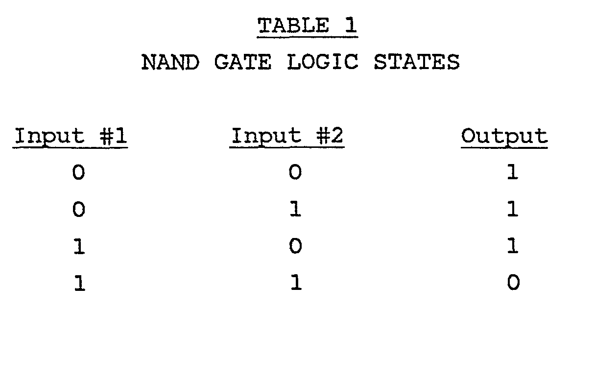

- Tables 1 and 2 summarize the logic states of the output signals for each possible combination of logic states for the input signals.
- Turning to Figures 3A and 3B a graph of the logic states of the timing signals as a function of time is shown. The logic states of the timing signals produced by the
timing circuit 39 vary from a low state, orlogic 0, to a high state, orlogic 1. From time TO to T1 the normal or steady-state condition of the timing signals is shown.Curve 105 represents the reset interval signal which is input to thegate 48. Thegate 48 acts as an inverter. The signal available at theoutput terminal 49 is represented bycurve 107 and is the inverse ofcurve 105. The reset signal is represented bycurve 109 and is input to thegate 51. Thereset signal 109 is normally high and effects a reset of the control circuit 36 by changing to a low state. The signal available at theoutput terminal 52 of thegate 51 is represented by curve 111 and is a combination ofcurves - Continuing the description of the steady-state condition of the
timing circuit 39, the signal available at theoutput terminal 59 of thegate 58 is the sample signal and is represented bycurve 113. Thegate 58 is responsive to the Q9 and Q10 output terminals of thecounter 56. The Q9 output terminal is representative of 29 or five hundred and twelve while the Q10 output terminal is representative of 210 or one thousand and twenty four. The signals available at these output terminals will either both be low or will be of opposite states until thecounter 56 reaches a count of one thousand five hundred and thirty six. Until this time the sample signal will be in a normally high state as shown bycurve 113. When thecounter 56 reaches a count of one thousand five hundred and thirty six the signals available at the Q9 and Q10 output terminals are both high and the sample signal changes from a high to a low state as shown at time T1 in Figure 3A. The rate of counting and the output terminals of thecounter 56 which are chosen determine the length of the predetermined time interval. With the sample signal in the low state the control circuit produces new sample values and effects a normal reset of the timing circuit, as discussed below, before thecounter 56 reaches a count of two thousand and forty eight. When this count is reached the signals available at the output terminals Q9 and Q10 both go low and the signal available at the output terminal Q11 changes from a normally low to a high state. - The signal available at the Q11 output terminal only goes high when the
counters counter 56 overflows because of continuous counting. The signal available at the Qll output terminal is input to thelogic gate 61. Thelogic gate 61 additionally receives the power failure signal PF which is normally in a low state. The output signal available at theoutput terminal 64 of thelogic gate 61 is normally in a high state. This signal is input to theNAND gate 66. - The signal available at the
output terminal 90 of thegate 89 is normally in a high state as shown bycurve 115 in Figure 3B since thegate 89 acts as an inverter. The voltage across thecapacitor 95 is represented bycurve 117. The voltage across thecapacitor 95 is normally in a low state responsive to the reset interval signal which is normally in a low state. The signal available at theoutput terminal 96 of thegate 92 is represented bycurve 119 which combines the effects ofcurves output terminal 96 is normally in a low state. Thegate 98 receives the signal represented bycurve 119 and the sample signal represented bycurve 113, The signal available at theoutput terminal 102 of thegate 98 is normally in a high state in response to these input signals. The signal available at the output terminal 67 of thegate 66 is normally in a low state since both inputs thereto are normally in a high state. The reset signal is available at theoutput terminal 75 of thegate 69 and is in a high state, as discussed earlier in conjunction withcurve 109, in response to the low state of the signal available at the output terminal 67 of thegate 66. - The signal available at the
output terminal 78 of thegate 77 is in a normally high state as represented bycurve 121 in response to the reset interval signal represented bycurve 105 and the reset signal represented bycurve 109. The voltage across thecapacitor 83 is in a normally high state as represented bycurve 123 in response to the high state of the signal available at theoutput terminal 78.Curve 125 represents the signal available at theoutput terminal 85 of thegate 80. The signal available at theoutput terminal 85 is normally in a low state since thegate 80 acts as an inverter. This concludes the description of the steady-state condition shown in Figures 3A and 3B from time TO to time Tl. - The normal reset of the
timing circuit 39 begins with the sample signal represented bycurve 113 changing from a high to a low state at time T1. While the sample signal is in the low state, the reset interval signal is momentarily in the high state as shown in Figure 3A from time T2 to time T3. The signal available at theoutput terminal 49 is the inverse of the reset voltage as shown bycurve 107. The combination of the signal available at theoutput terminal 49 and the reset signal causes the signal available at theoutput terminal 52 to be momentarily in a high state as shown by curve 111 in Figure 3A from time T2 to T3. When the signal at theoutput terminal 52 of thegate 51 is high, thecounters counters curve 113 at time T3. In summary, thecounters - During a normal reset of the
timing circuit 39 the sample signal represented bycurve 113 is in a low state. With a low signal input to thegate 98 the signal available at theoutput terminal 102 will be in a high state regardless of the state of the other input signal to thegate 98. Thus, during a normal reset thegates timing circuit 39. However, for purposes of analysis the signals produced by these gates will be discussed. At time T2 in Fig. 3B the signal available at theoutput terminal 90 changes from a high to a low state as shown bycurve 115. Simultaneously, thecapacitor 95 begins to charge in response to the reset interval signal being in a high state. Thegate 92 will produce a pulse, or spike, depending upon the value of thecapacitor 95 in response to the combination of the voltage across thecapacitor 95 and the signal available at theoutput terminal 90. This pulse, shown bycurve 119, is prevented from propagating through thegates output terminal 102 is held in a high state by the sample signal. In this manner thegates timing circuit 39 during a normal reset. - Similarly,
gates timing circuit 39 during a normal reset. As shown bycurve 121 in Fig. 3B, the signal available at theoutput terminal 78 changes from a high to a low state at time T2. With the signal available at theoutput terminal 78 in the low state thecapacitor 83 begins to discharge as shown bycurve 123. The discharge rate of thecapacitor 123 is such that thegate 80 continues to receive a high signal even though the signal available at theoutput terminal 78 has changed to a low state. The voltage available at theoutput terminal 78 returns to a high state at time T3 before thecapacitor 83 can discharge. Thus the signal available at theoutput terminal 85 ofgate 80 remains unchanged throughout the normal reset of thetiming circuit 39. - One failure mode which the
timing circuit 39 detects is a failure of the control circuit 36 to reset thetiming circuit 39. When the control circuit 36 fails to reset thetiming circuit 39, it is desirable to reset both thetiming circuit 39 and the control circuit 36. This result is effectuated by the signal available at the Qll output terminal of thecounter 56 changing from a normally low to a high state. This change occurs because of the continuous counting of thecounter 56 as discussed above. With the signal at the Qll output terminal in a high state the signal available at theoutput terminal 64 of thegate 61 changes from a high to a low state. With the low signal available at theoutput terminal 64 of thegate 61 input to theNAND gate 66 the signal available at the output terminal 67 changes from a normally low to a high state regardless of the other input to theNAND gate 66. The high state of the signal available at the output terminal 67 is inverted by thegate 69 causing the reset signal to change from a normally high to a low state. With the sample signal in a low state the control circuit 36 will be reset. Additionally, the signal available at theoutput terminal 52 of thegate 51 will change to a high state regardless of the state of the other input signal to thegate 51. With the signal available at theoutput terminal 52 in a high state the counters will be reset and the Qll signal will return to its normally low state. This allows all of the timing signal produced by thereset circuit 39 to return to their steady-state conditions. In summary, both the control circuit 36 and thetiming circuit 39 are reset by the signal available at the Q11 output terminal of thecounter 56 in response to a failure of the control circuit 36 to reset thetiming circuit 39. - The
timing circuit 39 will also recognize when the supply voltage is out of regulation and will hold the control circuit 36 in a reset condition until the supply voltage returns within its predetermined limits. This is effectuated by the power failure signal PF changing from a normally low to a high state. This change of state will propagate through thegates counter 56. The reset signal will be held in a low state so long as the power failure signal PF is in a high state. - Another failure mode of the control circuit 36 which the
timing circuit 39 recognizes is an attempt by the control circuit 36 to reset thetiming circuit 39 during an inappropriate time. As mentioned above the appropriate times for the control circuit 36 to reset thetiming circuit 39 are determined by the cooperation of the sample signal and theNAND gate 98. The appropriate time for atiming circuit 39 reset is when the sample signal is in a low state, which is referred to as a timing window. An inappropriate time for atiming circuit 39 reset is when the sample signal is in a high state, which is referred to as outside the timing window. Turning to Fig. 3B, thegates timing circuit 39 outside of the timing window the sample signal is in a high state. Since the sample signal is in a high state the pulse produced at theoutput terminal 96 is allowed to propagate through thegates timing circuit 39 return to their steady-state conditions. In summary, thegates timing circuit 39 outside of the timing window. - Another failure mode of the control circuit 36 which the
timing circuit 39 recognizes is a reset pulse of inappropriate duration within the timing window. This is shown in Figs. 3A and 3B beginning at time T5. In Fig. 3A, at time T5 the reset interval signal changes from a low to a high state as in the case of a normal reset. However, the reset interval signal remains in the high state for an inappropriate period of time. The sample signal represented bycurve 113 is in a low state such thatgate 98 and the pulse produced by the cooperation ofgates output terminal 78 of thegate 77 changes from a high to a low state. Because the reset interval signal remains in a high state for an inappropriate duration the signal available at thegate 78 remains in a low state for an inappropriate duration thus allowing thecapacitor 83 to discharge. The voltage across thecapacitor 83 is represented bycurve 123 and can be seen at time T6 to have sufficiently discharged to allow the output signal available at theoutput terminal 85 ofgate 80 to change from a normally low to a high state. This change in state causes the reset signal to change state which in turn resets the control circuit 36. With the control circuit 36 reset the reset interval signal returns to zero shortly after time T6. With the reset interval signal returned to its steady-state condition the signal available at theoutput terminal 78 returns to a high state thus chargingcapacitor 83. At time T7 thecapacitor 83 has sufficiently charged such that the signal available at theoutput terminal 85 returns to a steady-state condition. With the return of thesignal 85 to its steady-state condition the remainder of the timing signals of thetiming circuit 39 return to their steady-state conditions. The value of thecapacitor 83 may be chosen so as to limit the duration of acceptable reset interval pulses. In summary, thegates timing circuit 39. - Turning to Fig. 4 an electrical schematic illustrating the details of the ranging
amplifiers 30 is shown. Theconductors multiplexer 31. The conductor 20 carries the sample values representative of the instantaneous magnitude of the current component signal IA which are input both to themultiplexer 31 and to a non-inverting input terminal of anoperational amplifier 128 through aresistor 130. The non-inverting input terminal is connected to ground through acapacitor 131. An inverting input terminal of theoperational amplifier 128 is connected to ground through aresistor 132. The inverting input terminal of theoperational amplifier 128 is connected to an output terminal thereof through acapacitor 133 parallel connected with the series combination ofresistors operational amplifier 128 is connected to an input terminal of themultiplexer 31 through aresistor 138. The input terminal is connected to a positive voltage source through adiode 139 and to a negative voltage source through adiode 140. - The
conductor 21 carries the sample values representative of the instantaneous magnitude of the current component signal IB which are input both to themultiplexer 31 and to a non-inverting input terminal of anoperational amplifier 141 through aresistor 143. The non-inverting input terminal is connected to ground through acapacitor 144. An inverting input terminal of theoperational amplifier 141 is connected to ground through a resistor 146. The inverting input terminal of theoperational amplifier 141 is connected to an output terminal thereof through acapacitor 147 parallel connected with the series combination ofresistors operational amplifier 141 is connected to an input terminal of themultiplexer 31 through aresistor 152. The input terminal is connected to a positive voltage source through a diode 153 and to a negative voltage source through adiode 154. - Finally, the
conductor 22 carries the sample values representative of the instantaneous magnitude of the current component signal IC which are input to both themultiplexer 31 and to a non-inverting input terminal of anoperational amplifier 155 through aresistor 157. The non-inverting input terminal is connected to ground through acapacitor 158. An inverting input terminal of theoperational amplifier 155 is connected to ground through a resistor 160. The inverting input terminal of theoperational amplifier 155 is connected to an output terminal thereof through acapacitor 161 parallel connected with the series combination of resistors 162, 163 and 164. The output terminal of theoperational amplifier 155 is connected to an input terminal of themultiplexer 31 through aresistor 166. The input terminal is connected to a positive voltage source through adiode 167 and a negative voltage source through adiode 168. - The
operational amplifiers operational amplifier 128 is determined by theresistors resistors operational amplifiers resistors multiplexer 31 are clamped to acceptable values. The rangingamplifiers 30 have been found to significantly increase the overall accuracy of themetering system 10.
Claims (16)
1. An AC electric energy metering system for calculating a plurality of indicia of an AC electric energy quantity delivered by an electric utility system, said metering system comprising:
signal sample means [Fig. 1(12, 14)] including inputs and outputs, said inputs receiving line voltages (VA, VB, VC) and currents (IA, IB' IC) determining the magnitude of the AC electric energy quantity, said outputs producing sample values representative of the instantaneous magnitudes of said line voltages and currents when said signal sample means is rendered to a sampling state;
sample timer means [Figs. 1, 2 (39)] producing a sample signal (42) having first and second states, said first state occurring at randomly varying intervals and rendering said signal sample means to said sampling state at randomly occurring sampling times;
analog-to-digital converter means (33) producing binary signal representations of each of said sample values;
control means (36) calculating the plurality of indicia of said AC electric energy quantity from said binary signal representations of each of said sample values, said control means producing a reset interval signal (40) composed of pulses, said pulses resetting said sample timer means; and characterized by:
means [Fig. 2 (39)] resetting (43) said control means when a pulse of said reset interval signal is input to said sample timer means while said sample signal is in said second state;
output means (45) connected to said control means, for producing data output signals representative of said plurality of indicia of said AC electric energy quantity.
2. The system as claimed in claim 1 including a source (41) of clock pulses, and wherein the sample timer means includes a counter (Fig. 2 (54)] responsive to said clock pulses.
3. The system as claimed in claim 1 or 2 wherein the means producing the sample signal includes a NAND gate (58) responsive to the counter, the first state of said sample signal being representative of the proper times to reset the sample timer means, the second state of said sample signal being representative of the improper times to reset said sample timer means.
4. The system as claimed in claim 3 wherein the resetting means produces a reset signal (43) in response to a pulse of the reset interval signal being input to the sample timer means while said sample signal is in the second state.
5. The system as claimed in claim 3 or 4 wherein the resetting means includes an inverter (89) responsive to the reset interval signal, means for delaying (95) said reset interval signal, a first gate (92) responsive to both the inverted reset interval signal and the delayed reset interval signal, and a second gate (98) responsive to both the sample signal and said first gate.
6. The system as claimed in claim 5 wherein the means for delaying includes a capacitor, and wherein the first gate includes a NOR gate and wherein the second gate includes a NAND gate.
7. The system as claimed in any one of claims 1 to 6 including means for resetting (61, 69) both the sample timer means and the control means when said control means fails to reset said sample timer means.
8. The system as claimed in claim 7 when dependent through claim 2, wherein the sample timer means includes a second counter [Fig. 2 (56)], and wherein the resetting means includes a NOR gate (61) responsive to an overflow output (Qll) terminal of said counter and a NAND gate (66) responsive to the output of said NOR gate for resetting both the sample timer means and the control means.
9. The system as claimed in claim 1 or 8 including second resetting means [Fig. 2 (77, 80)] for the control means when a pulse of the reset interval signal of inappropriate duration is input to the sample timer means while the sample signal is in the first state.
10. The system as claimed in claim 9 wherein the inappropriate duration includes DC signals, and the second resetting means includes a first NAND gate (77) responsive to the reset interval signal, a capacitor connected (83) for delaying responsive to said first gate, and an inverter (80) responsive to the output of said first gate as modified by the capacitive delaying.
11. The system as claimed in claim 8 including a power supply (PF) producing a regulated suply voltage, and including a connection (62) to said NOR gate responsive to an overflow output terminal for means for resetting the control means in response to said supply voltage being out of regulation.
12. The system as claimed in claim 11 wherein the control means is held in the reset condition so long as the supply voltage is out of regulation.
13. The system as claimed in claim 1 or 2 including ranging amplifiers [Figs. 1, 4 (30)] responsive to the sample values of the line currents.
14. The system of claim 17 including means for multiplexing, said means responsive to both the signal sample means and the ranging amplifiers.
15. The system as claimed in claim 13 or 14 wherein the ranging amplifiers include non-inverting amplifiers (128, 141, 155) having a gain that is a power of two.
16. An AC electric energy metering system, substantially as hereinbefore described with reference to and as illustrated in the accompanying drawings.
Applications Claiming Priority (2)
| Application Number | Priority Date | Filing Date | Title |
|---|---|---|---|
| US06/224,871 US4365302A (en) | 1981-01-14 | 1981-01-14 | High accuracy AC electric energy metering system |
| US224871 | 1981-01-14 |
Publications (1)
| Publication Number | Publication Date |
|---|---|
| EP0057978A1 true EP0057978A1 (en) | 1982-08-18 |
Family
ID=22842575
Family Applications (1)
| Application Number | Title | Priority Date | Filing Date |
|---|---|---|---|
| EP82300195A Ceased EP0057978A1 (en) | 1981-01-14 | 1982-01-14 | High accuracy AC electric energy metering system |
Country Status (9)
| Country | Link |
|---|---|
| US (1) | US4365302A (en) |
| EP (1) | EP0057978A1 (en) |
| JP (1) | JPS57137863A (en) |
| KR (1) | KR830009489A (en) |
| AU (1) | AU7916182A (en) |
| BR (1) | BR8200153A (en) |
| CA (1) | CA1180760A (en) |
| MX (1) | MX150583A (en) |
| ZA (1) | ZA8271B (en) |
Cited By (14)
| Publication number | Priority date | Publication date | Assignee | Title |
|---|---|---|---|---|
| FR2543302A1 (en) * | 1983-03-24 | 1984-09-28 | Electricite De France | Apparatus for metering on command and reading by telephone line |
| FR2563013A1 (en) * | 1984-04-17 | 1985-10-18 | Sauter Ag | ELECTRONIC ENERGY CONSUMPTION COUNTER AND ELECTRIC ENERGY MEASURING METHOD WITH ENERGY CONSUMPTION COUNTER |
| EP0201019A1 (en) * | 1985-05-02 | 1986-11-12 | Zellweger Uster Ag | Static electricity-meter and method for its calibration |
| US4641090A (en) * | 1984-10-22 | 1987-02-03 | Refac Electronics Corporation | Polyphase electrical signal measuring apparatus |
| EP0288413A1 (en) * | 1987-04-24 | 1988-10-26 | Transdata, Inc. | Digital power metering |
| FR2617310A1 (en) * | 1987-06-26 | 1988-12-30 | Kalfon Rene | Centralised metering device especially for electrical energy consumption |
| US4884021A (en) * | 1987-04-24 | 1989-11-28 | Transdata, Inc. | Digital power metering |
| FR2645969A1 (en) * | 1989-02-01 | 1990-10-19 | Gen Electric | METHOD AND APPARATUS FOR CONTROLLING POWER FOR DISTRIBUTION OF ELECTRICAL ENERGY |
| EP0420545A3 (en) * | 1989-09-25 | 1992-07-08 | General Electric Company | Electronic watthour meter |
| US5245275A (en) * | 1989-09-25 | 1993-09-14 | General Electric Company | Electronic watthour meter |
| US5258704A (en) * | 1989-09-25 | 1993-11-02 | General Electric Company | Electronic watthour meter |
| US5289115A (en) * | 1989-09-25 | 1994-02-22 | General Electric Company | Electronic watt-hour meter with selection of time base signals |
| WO2007038537A1 (en) * | 2005-09-27 | 2007-04-05 | Microchip Technology Incorporated | Selectable real time sample triggering for a plurality of inputs of an analog-to-digital converter |
| CN104049141A (en) * | 2012-02-27 | 2014-09-17 | 华立仪表集团股份有限公司 | Load controlling method of intelligent and integral multifunction watt-hour meter |
Families Citing this family (40)
| Publication number | Priority date | Publication date | Assignee | Title |
|---|---|---|---|---|
| JPS5854825A (en) * | 1981-09-29 | 1983-03-31 | 株式会社東芝 | Protective relay unit |
| US4445183A (en) * | 1981-12-23 | 1984-04-24 | Rockwell International Corporation | Electrical switch |
| JPS5948659A (en) * | 1982-09-13 | 1984-03-19 | Ohkura Electric Co Ltd | Multiplexing measuring apparatus of electric circuit |
| US4581705A (en) * | 1983-01-28 | 1986-04-08 | Cooper Industries, Inc. | Method and machine for metering electric parameters |
| US4615009A (en) * | 1983-02-16 | 1986-09-30 | Transdata, Inc. | Electronic energy and power monitoring apparatus |
| JPS6085371A (en) * | 1983-10-17 | 1985-05-14 | Mitsubishi Electric Corp | Ac measuring apparatus |
| US4783748A (en) * | 1983-12-09 | 1988-11-08 | Quadlogic Controls Corporation | Method and apparatus for remote measurement |
| JPS61221676A (en) * | 1984-01-27 | 1986-10-02 | Mitsubishi Electric Corp | Detector processor for various electric quantities |
| JPH0723899B2 (en) * | 1984-04-05 | 1995-03-15 | 三菱電機株式会社 | Electric quantity detection processing device |
| US4672555A (en) * | 1984-10-18 | 1987-06-09 | Massachusetts Institute Of Technology | Digital ac monitor |
| FR2578091B1 (en) * | 1985-02-25 | 1988-08-05 | Merlin Gerin | CIRCUIT BREAKER WITH DIGITAL STATIC TRIGGER PROVIDED WITH A CALIBRATION CIRCUIT |
| US4626769A (en) * | 1985-03-13 | 1986-12-02 | Analog Devices, Inc. | Voltage/current source |
| JPH07117560B2 (en) * | 1985-10-31 | 1995-12-18 | 三菱電機株式会社 | Power converter |
| DE3611680A1 (en) * | 1986-04-08 | 1987-10-15 | Bbc Brown Boveri & Cie | Method for measurement conversion |
| US4933676A (en) * | 1989-06-12 | 1990-06-12 | Technology 80, Inc. | Programmable multi-input A/D converter |
| US5151866A (en) * | 1990-03-30 | 1992-09-29 | The Dow Chemical Company | High speed power analyzer |
| JPH06190029A (en) * | 1992-12-22 | 1994-07-12 | Shin Nippon Giken Kogyo Kk | Apparatus and method for air purification by using ozone in purification room |
| US5650936A (en) * | 1994-12-30 | 1997-07-22 | Cd Power Measurement Limited | Power monitor apparatus and method with object oriented structure |
| US5736847A (en) * | 1994-12-30 | 1998-04-07 | Cd Power Measurement Limited | Power meter for determining parameters of muliphase power lines |
| US5994892A (en) * | 1996-07-31 | 1999-11-30 | Sacramento Municipal Utility District | Integrated circuit design automatic utility meter: apparatus & method |
| US6186842B1 (en) | 1999-08-09 | 2001-02-13 | Power Measurement Ltd. | Revenue meter bayonet assembly and method of attachment |
| US6825776B2 (en) * | 1999-08-09 | 2004-11-30 | Power Measurement Ltd. | External I/O and communications interface for a revenue meter |
| US6493644B1 (en) | 1999-08-09 | 2002-12-10 | Power Measurement Ltd. | A-base revenue meter with power quality features |
| US6798191B1 (en) | 1999-08-09 | 2004-09-28 | Power Measurement Ltd. | Revenue meter with a graphic user interface being operative to display scalable objects |
| US6611922B2 (en) | 1999-08-09 | 2003-08-26 | Power Measurement, Ltd. | Power system time synchronization device and method for sequence of event recording |
| US6397155B1 (en) | 1999-08-09 | 2002-05-28 | Power Measurement Ltd. | Method and apparatus for automatically controlled gain switching of monitors |
| US6615147B1 (en) | 1999-08-09 | 2003-09-02 | Power Measurement Ltd. | Revenue meter with power quality features |
| US7623043B2 (en) * | 2005-12-19 | 2009-11-24 | General Electric Company | Method and system for metering consumption of energy |
| MX2011009052A (en) | 2009-05-07 | 2012-02-28 | Dominion Resources Inc | Voltage conservation using advanced metering infrastructure and substation centralized voltage control. |
| US8975787B2 (en) | 2009-05-08 | 2015-03-10 | Computer Performance, Inc. | Reduced parts count isolated AC current switching and sensing |
| US8324885B2 (en) * | 2009-09-17 | 2012-12-04 | Tektronix, Inc. | Mixed signal acquisition system for a measurement instrument |
| TWI423549B (en) | 2010-07-02 | 2014-01-11 | Univ Nat Chiao Tung | Power monitoring device for identifying state of electric equipment and power monitoring method thereof |
| CN102590610B (en) * | 2012-02-27 | 2014-11-19 | 华立仪表集团股份有限公司 | Intelligent integral multifunctional electric energy meter and method for controlling load by same |
| US9563218B2 (en) | 2013-03-15 | 2017-02-07 | Dominion Resources, Inc. | Electric power system control with measurement of energy demand and energy efficiency using t-distributions |
| US9847639B2 (en) | 2013-03-15 | 2017-12-19 | Dominion Energy, Inc. | Electric power system control with measurement of energy demand and energy efficiency |
| US9582020B2 (en) | 2013-03-15 | 2017-02-28 | Dominion Resources, Inc. | Maximizing of energy delivery system compatibility with voltage optimization using AMI-based data control and analysis |
| US9678520B2 (en) | 2013-03-15 | 2017-06-13 | Dominion Resources, Inc. | Electric power system control with planning of energy demand and energy efficiency using AMI-based data analysis |
| US9553453B2 (en) | 2013-03-15 | 2017-01-24 | Dominion Resources, Inc. | Management of energy demand and energy efficiency savings from voltage optimization on electric power systems using AMI-based data analysis |
| US20160294500A1 (en) * | 2015-04-03 | 2016-10-06 | John Mezzalingua Associates, LLC | Packet energy transfer powered telecommunications system for macro antenna systems and power distribution system therefor |
| US10732656B2 (en) | 2015-08-24 | 2020-08-04 | Dominion Energy, Inc. | Systems and methods for stabilizer control |
Citations (2)
| Publication number | Priority date | Publication date | Assignee | Title |
|---|---|---|---|---|
| US4077061A (en) * | 1977-03-25 | 1978-02-28 | Westinghouse Electric Corporation | Digital processing and calculating AC electric energy metering system |
| EP0008630A1 (en) * | 1978-07-17 | 1980-03-19 | Siemens Aktiengesellschaft | Power/frequency converter with a microcomputer |
Family Cites Families (6)
| Publication number | Priority date | Publication date | Assignee | Title |
|---|---|---|---|---|
| CH632847A5 (en) * | 1978-11-13 | 1982-10-29 | Landis & Gyr Ag | DEVICE FOR MEASURING ELECTRICAL PERFORMANCE IN AN AC NETWORK. |
| US4217651A (en) * | 1978-12-12 | 1980-08-12 | Datron Electronics Limited | Electrical measurements |
| US4335445A (en) * | 1979-02-26 | 1982-06-15 | Kepco, Inc. | System for interfacing computers with programmable power supplies |
| US4301508A (en) * | 1979-03-28 | 1981-11-17 | Eaton Corp. | Digital processing system for time-of-day and demand meter display |
| US4261037A (en) * | 1979-04-03 | 1981-04-07 | Dupont Energy Management Corporation | System for monitoring utility usage |
| US4291376A (en) * | 1979-08-08 | 1981-09-22 | Three Rivers Enterprises, Inc. | Digital energy monitor |
-
1981
- 1981-01-14 US US06/224,871 patent/US4365302A/en not_active Expired - Fee Related
-
1982
- 1982-01-04 AU AU79161/82A patent/AU7916182A/en not_active Abandoned
- 1982-01-06 ZA ZA8271A patent/ZA8271B/en unknown
- 1982-01-07 CA CA000393714A patent/CA1180760A/en not_active Expired
- 1982-01-11 JP JP57001866A patent/JPS57137863A/en active Granted
- 1982-01-13 MX MX190963A patent/MX150583A/en unknown
- 1982-01-13 BR BR8200153A patent/BR8200153A/en unknown
- 1982-01-14 KR KR1019820000131A patent/KR830009489A/en unknown
- 1982-01-14 EP EP82300195A patent/EP0057978A1/en not_active Ceased
Patent Citations (3)
| Publication number | Priority date | Publication date | Assignee | Title |
|---|---|---|---|---|
| US4077061A (en) * | 1977-03-25 | 1978-02-28 | Westinghouse Electric Corporation | Digital processing and calculating AC electric energy metering system |
| GB1578174A (en) * | 1977-03-25 | 1980-11-05 | Westinghouse Electric Corp | Digital processing and calculating ac electric energy metering system |
| EP0008630A1 (en) * | 1978-07-17 | 1980-03-19 | Siemens Aktiengesellschaft | Power/frequency converter with a microcomputer |
Non-Patent Citations (1)
| Title |
|---|
| Archiv fur Technisches Messen, No. 6 June 1974 D. Funke "Ein Digitales Energiemessverfahren" pages 107 to 112 * page 111, paragraph 4.2 to page 112, paragraph 5; fig. 7 * * |
Cited By (17)
| Publication number | Priority date | Publication date | Assignee | Title |
|---|---|---|---|---|
| FR2543302A1 (en) * | 1983-03-24 | 1984-09-28 | Electricite De France | Apparatus for metering on command and reading by telephone line |
| FR2563013A1 (en) * | 1984-04-17 | 1985-10-18 | Sauter Ag | ELECTRONIC ENERGY CONSUMPTION COUNTER AND ELECTRIC ENERGY MEASURING METHOD WITH ENERGY CONSUMPTION COUNTER |
| EP0161447A1 (en) * | 1984-04-17 | 1985-11-21 | Fr. Sauter AG Fabrik elektr. Apparate | Electronic energy consumption meter |
| US4641090A (en) * | 1984-10-22 | 1987-02-03 | Refac Electronics Corporation | Polyphase electrical signal measuring apparatus |
| US4837504A (en) * | 1985-05-02 | 1989-06-06 | Zellweger Uster Ltd. | Electricity meter and method of calibrating same |
| EP0201019A1 (en) * | 1985-05-02 | 1986-11-12 | Zellweger Uster Ag | Static electricity-meter and method for its calibration |
| US4884021A (en) * | 1987-04-24 | 1989-11-28 | Transdata, Inc. | Digital power metering |
| EP0288413A1 (en) * | 1987-04-24 | 1988-10-26 | Transdata, Inc. | Digital power metering |
| FR2617310A1 (en) * | 1987-06-26 | 1988-12-30 | Kalfon Rene | Centralised metering device especially for electrical energy consumption |
| FR2645969A1 (en) * | 1989-02-01 | 1990-10-19 | Gen Electric | METHOD AND APPARATUS FOR CONTROLLING POWER FOR DISTRIBUTION OF ELECTRICAL ENERGY |
| EP0420545A3 (en) * | 1989-09-25 | 1992-07-08 | General Electric Company | Electronic watthour meter |
| US5245275A (en) * | 1989-09-25 | 1993-09-14 | General Electric Company | Electronic watthour meter |
| US5258704A (en) * | 1989-09-25 | 1993-11-02 | General Electric Company | Electronic watthour meter |
| US5289115A (en) * | 1989-09-25 | 1994-02-22 | General Electric Company | Electronic watt-hour meter with selection of time base signals |
| WO2007038537A1 (en) * | 2005-09-27 | 2007-04-05 | Microchip Technology Incorporated | Selectable real time sample triggering for a plurality of inputs of an analog-to-digital converter |
| CN104049141A (en) * | 2012-02-27 | 2014-09-17 | 华立仪表集团股份有限公司 | Load controlling method of intelligent and integral multifunction watt-hour meter |
| CN104049141B (en) * | 2012-02-27 | 2017-01-04 | 华立科技股份有限公司 | The Intelligent integrated formula multifunctional electric energy meter control method to load |
Also Published As
| Publication number | Publication date |
|---|---|
| KR830009489A (en) | 1983-12-21 |
| US4365302A (en) | 1982-12-21 |
| CA1180760A (en) | 1985-01-08 |
| JPS57137863A (en) | 1982-08-25 |
| JPS6360865B2 (en) | 1988-11-25 |
| AU7916182A (en) | 1982-07-22 |
| MX150583A (en) | 1984-05-30 |
| ZA8271B (en) | 1983-01-26 |
| BR8200153A (en) | 1982-11-03 |
Similar Documents
| Publication | Publication Date | Title |
|---|---|---|
| US4365302A (en) | High accuracy AC electric energy metering system | |
| US5391983A (en) | Solid state electric power usage meter and method for determining power usage | |
| EP0085769B1 (en) | Electricity meters | |
| US9696357B2 (en) | Element resistance measurement in an electricity meter | |
| US5124624A (en) | Arrangement for electrical measurement | |
| EP0360605B1 (en) | Apparatus for measuring capacitance | |
| JPH09508968A (en) | Battery monitoring device adjusted by current rate | |
| US4103225A (en) | System and method for determining capacitance and cable length in the presence of other circuit elements | |
| GB1578174A (en) | Digital processing and calculating ac electric energy metering system | |
| US4712195A (en) | Solid-state cumulative operations measurement system | |
| CA1233228A (en) | Method for determining the time of reclosing a circuit breaker and device for carrying out this method | |
| JPH10508460A (en) | Digital fine-tuning of on-chip analog components | |
| JPH0812222B2 (en) | Digital fault locator | |
| US4594545A (en) | Operation of electronic demand register following a power outage | |
| US4459545A (en) | Apparatus for detecting a current peak value and a voltage peak value | |
| US4146836A (en) | Power monitor | |
| US3264541A (en) | Analog to digital pulse rate integrator and motor driven counter therefor | |
| KR900000983B1 (en) | Electronic lectric power meter | |
| GB1206302A (en) | Improvements in testing arrangements for electricity meters | |
| CA1233517A (en) | Test operation of electronic demand register | |
| SU1661686A2 (en) | Apparatus for insulation preliminary automatic control of electric circuit portion | |
| JPS6060567A (en) | Electronic type watt-hour meter | |
| Dewe et al. | A Microprocessor Based Inverse Time Overcurrent Relay | |
| SU1187112A1 (en) | Apparatus for determining distance to place of short circuit in power line | |
| JPS5835697A (en) | Measuring apparatus |
Legal Events
| Date | Code | Title | Description |
|---|---|---|---|
| PUAI | Public reference made under article 153(3) epc to a published international application that has entered the european phase |
Free format text: ORIGINAL CODE: 0009012 |
|
| AK | Designated contracting states |
Designated state(s): CH DE FR GB IT |
|
| 17P | Request for examination filed |
Effective date: 19830216 |
|
| STAA | Information on the status of an ep patent application or granted ep patent |
Free format text: STATUS: THE APPLICATION HAS BEEN REFUSED |
|
| 18R | Application refused |
Effective date: 19850425 |
|
| RIN1 | Information on inventor provided before grant (corrected) |
Inventor name: ELMS, ROBERT TRACY |