EP0061403A1 - Drift compensating device for at least a single measuring channel, and its application - Google Patents
Drift compensating device for at least a single measuring channel, and its application Download PDFInfo
- Publication number
- EP0061403A1 EP0061403A1 EP82400507A EP82400507A EP0061403A1 EP 0061403 A1 EP0061403 A1 EP 0061403A1 EP 82400507 A EP82400507 A EP 82400507A EP 82400507 A EP82400507 A EP 82400507A EP 0061403 A1 EP0061403 A1 EP 0061403A1
- Authority
- EP
- European Patent Office
- Prior art keywords
- measurement
- signal
- circuit
- chain
- output
- Prior art date
- Legal status (The legal status is an assumption and is not a legal conclusion. Google has not performed a legal analysis and makes no representation as to the accuracy of the status listed.)
- Granted
Links
Images


Classifications
-
- G—PHYSICS
- G01—MEASURING; TESTING
- G01S—RADIO DIRECTION-FINDING; RADIO NAVIGATION; DETERMINING DISTANCE OR VELOCITY BY USE OF RADIO WAVES; LOCATING OR PRESENCE-DETECTING BY USE OF THE REFLECTION OR RERADIATION OF RADIO WAVES; ANALOGOUS ARRANGEMENTS USING OTHER WAVES
- G01S7/00—Details of systems according to groups G01S13/00, G01S15/00, G01S17/00
- G01S7/02—Details of systems according to groups G01S13/00, G01S15/00, G01S17/00 of systems according to group G01S13/00
- G01S7/28—Details of pulse systems
- G01S7/2813—Means providing a modification of the radiation pattern for cancelling noise, clutter or interfering signals, e.g. side lobe suppression, side lobe blanking, null-steering arrays
-
- G—PHYSICS
- G01—MEASURING; TESTING
- G01S—RADIO DIRECTION-FINDING; RADIO NAVIGATION; DETERMINING DISTANCE OR VELOCITY BY USE OF RADIO WAVES; LOCATING OR PRESENCE-DETECTING BY USE OF THE REFLECTION OR RERADIATION OF RADIO WAVES; ANALOGOUS ARRANGEMENTS USING OTHER WAVES
- G01S7/00—Details of systems according to groups G01S13/00, G01S15/00, G01S17/00
- G01S7/02—Details of systems according to groups G01S13/00, G01S15/00, G01S17/00 of systems according to group G01S13/00
- G01S7/28—Details of pulse systems
- G01S7/285—Receivers
-
- H—ELECTRICITY
- H01—ELECTRIC ELEMENTS
- H01Q—ANTENNAS, i.e. RADIO AERIALS
- H01Q21/00—Antenna arrays or systems
- H01Q21/29—Combinations of different interacting antenna units for giving a desired directional characteristic
-
- H—ELECTRICITY
- H03—ELECTRONIC CIRCUITRY
- H03F—AMPLIFIERS
- H03F1/00—Details of amplifiers with only discharge tubes, only semiconductor devices or only unspecified devices as amplifying elements
- H03F1/30—Modifications of amplifiers to reduce influence of variations of temperature or supply voltage or other physical parameters
- H03F1/303—Modifications of amplifiers to reduce influence of variations of temperature or supply voltage or other physical parameters using a switching device
Definitions
- the present invention relates to a device for compensating for drifts of at least one measurement chain and its application to a device for compensating the secondary lobes of a secondary radar.
- the compensation of the drifts of the amplifiers used to amplify impulse signals is carried out in the prior art by taking into account only the drifts of the zero of the amplifier as a function of the stability of the supply voltage, of the temperature of the ambient medium. , time, etc. Compensation is then carried out by simple translation of the input-output characteristic of the amplifier.
- Such a device is described, for example, in French patent No. 2,415,390.
- the subject of the invention is therefore a device making it possible to compensate for the drifts of the amplifiers arranged in the measurement chains, whatever the form in which these drifts appear.
- a device for compensating for the drifts of a measurement chain comprises a circuit applying to said measurement chain a measurement input signal, and a reference input signal to which correspond respectively a measurement output signal. , and a reference output signal, a memory storing the value of said reference output signal, and a subtracting circuit subtracting said stored value from the measurement output signal.
- the invention also relates to a device for compensating for the drifts of two measurement chains mounted in differential, which comprises a circuit applying to each of the measurement chains a measurement input signal, and a reference input signal to which correspond respectively for each chain a measurement output signal, and a reference output signal, a circuit memorizing the value of the reference output signal respectively for one chain and for the other, and a subtractor circuit subtracting respectively from each of the signals measurement output the corresponding memorized value, and also performing the subtraction between them of the results of the two previous subtractions.
- the invention relates to a device for compensating for the drifts of two differential-mounted measurement chains, which comprises a circuit applying to each measurement chain a measurement input signal and a reference input signal, to which correspond respectively. for each chain a measurement output signal, and a reference output signal, a circuit memorizing the difference of the values of the reference output signals respectively for one chain and for the other, and a subtractor circuit performing the subtraction of the signals of each of the measurement chains and subtracting said stored difference from them.
- a device according to the invention can advantageously be applied to a device for compensating the secondary lobes of a secondary radar for which a measurement signal is the signal of a first receiver associated with the secondary radar and the other measurement signal is the signal from a second receiver associated with the secondary radar.
- FIG. 1a represents a compensation device, where a device 2 which can be a switching device introduced into a measuring chain 3 a signal coming from a detector 1, and / or a reference signal produced by a circuit l ' .
- the circuit 2 is controlled by a line 8 which also controls the switching of a memory 4 between a write position when the chain 3 receives a reference signal, and a read position when the chain 3 receives a measurement signal.
- the measurement signal s 1m , and the reference signal s 1r present at the output of the memory 4 are introduced at the two inputs of an operational amplifier 5 mounted as a subtractor.
- Amplifier 5 includes a resistance of feedback R 6 and two input resistors R 6 respectively at its inverting and non-inverting input terminals, as well as a resistor R 6 between its non-inverting input and ground.
- the output signal S 1 of the amplifier 5 is the difference between the stored measurement signal and the reference signal.
- the set of characteristics of this one converge in a point of zero ordinate and of abscissa G, G being the reference quantity applied to the input of the measuring chain. It follows that the compensation is perfectly carried out at the level of the reference value, and approximately around this value, the approximation being however of the second order, that is to say negligible in practice.
- Circuit 2 can be controlled by line 8 at regular intervals so as to take account of changes in drift.
- FIG. 2 represents a device for compensating for the drifts of two differential measurement chains which each deliver output signals s 1 and s 2 respectively . These signals are introduced at the positive input of two differential amplifiers 16 and 26 respectively. The values stored in memories 14 and 24 respectively and corresponding to reference output signals, are introduced at the negative input of the differential amplifiers 16 and 26.
- the amplifier 16 is provided with a feedback resistance R 15 and two input resistors R 15 each arranged its inverting and non-inverting inputs, as well as a resistor R1 5 disposed between its non-inverting input. inverting and ground.
- the amplifier 26, in the same way, is provided with a feedback resistance R 25 and two input resistors R 25 disposed respectively at the inverting and non-inverting inputs, as well as a resistor R 25 disposed between its non-inverting input and ground.
- the output signals of amplifiers 16 and 26 are introduced respectively to the negative and positive inputs of a differential amplifier 11 provided with a feedback resistance R 10 and two input resistors R 10 arranged at its inverting input and at its non-inverting input, as well as a resistor R 10 disposed between its non-inverting input and the ground.
- the gains of amplifiers 11, 16 and 26 at their different inputs can of course be chosen to be different from 1, provided that the identical measured quantities on each of the two measuring chains correspond to identical values at the output of amplifier 11 Under these conditions, the output 5 2 will correspond, to within a multiplicative factor, with the difference:
- FIG. 3 represents a variant of FIG. 2 where the difference of the reference output signals is stored in a memory 33, for example by using a differential amplifier 31 receiving at each of its inputs the output signals of the two measurement chains, this amplifier being provided with a feedback resistance R 30 and two input resistors with a value also equal to R 30 .
- the output of memory 33 is introduced at the negative input of a differential amplifier 35 which receives at its other input the measurement output signal s 2m .
- This amplifier is provided with a feedback resistance R 34 and two input resistors R 34 as well as a resistance R 34 between its non-inverting input and ground.
- the output of an amplifier 35 is introduced to the positive input of an amplifier differential 38 which receives at its negative input the measurement signal s 1m from the first measurement chain.
- Amplifier 38 is provided with a feedback resistance R37, two input resistors R37 and a resistance R 37 between its non-inverting input and ground.
- the overall gains being, as in the previous case, balanced, the output S 3 of the differential amplifier 38 corresponds to the output 5 2 of FIG. 2.
- FIG. 4 also shows a variant relating to the compensation of two differential measurement chains.
- the output signals s 1 and s 2 of the two measuring chains are introduced to the negative and positive inputs of a differential amplifier 41 provided with a feedback resistance R 46 and two input resistors R 46 as well as d 'a resistor R 46 between its non-inverting input and ground.
- the output of amplifier 41 is introduced into a memory 43 by a line 42, and the output 44 corresponding to the reading of the memory is introduced at the negative input of amplifier 41, also through an input resistor R 46 .
- the signal 5 4 corresponds to the output signals S 2 and S 3 of FIGS. 2 and 3.
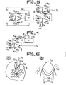
- FIG. 5 a represents the angular diagrams corresponding to antennas with multiple diagrams the shapes of which are defined so as to be able to better delimit the interrogation arc and to discriminate the responses coming from a main lobe and those coming from the secondary lobes.
- the diagram RS1 presents a main lobe 53 provided with a maximum 54 which corresponds to the geometric axis of the antenna, and a plurality of secondary lobes 55 of lower amplitude.
- the RS2 diagram is in the general form of a cardioid and has a minimum gain of 52 in the main direction constituting the geometric axis of the antenna.
- the RS2 diagram corresponds to an amplitude greater than that of all the secondary lobes 55.
- Figure 5b illustrates the variation of the interrogation arc which can be obtained by adding a constant to the RS2 diagram: the interrogation arc a 2 located closer to the top of RS1 is thus narrower than the arc d 'interrogation a I , which allows a finer interrogation.
- FIG. 6 illustrates the application of a device according to the invention to the compensation of the measurement chains of an RSLS system.
- the compensation will take place by periodically effecting, outside the normal use time of the receiver, the storage of the amplitude of the response associated with a signal of known amplitude. for each of the receivers.
- the response of the receiver to an input signal of any amplitude will be compared to the stored response in order to take into account only the difference between these two signals.
- FIG. 6 thus represents a device corresponding to a diagram equivalent to FIGS. 2 to 4, where the measurement values present at the output of the two chains sri and s r2 are applied respectively to the positive and negative inputs of a differential amplifier 63 provided with a feedback resistance R62, through input resistors R 62 , and where the values memorized respectively by the memories 61 and 62 present at the output of said measurement chains, are applied respectively to the negative and positive inputs of the amplifier differential 63 through R 62 input resistors.
- the compensated signal S6 present at the output of the amplifier 63 will have a positive sign for the signals corresponding to the main lobes 53 of the RSI diagram.
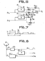
- FIG. 7 illustrates a mode of temporal distribution between the measurement signals and the reference signals in the case of the radar technique.
- the recurrent radar pulses I are separated by time intervals T.
- the measurement takes place during the time interval T 1
- FIG. 8 illustrates the switching carried out at the level of an antenna 81.
- a synchronization pulse brought by a line 86 simultaneously controls an oscillator 83 coupled to the output of the antenna 81 by a coupler 82, and the writing into a memory 85. This will result in a reference pulse applied to the input of the measurement chain 84 as long as. the synchronization pulse is present.
- the stored value S remains permanently present at the - exit from memory M.
- Such a device is particularly advantageous in the case of the technique considered since it constitutes not only compensation for drifts in the reception chain but also compensation for the interference that the radar antenna is capable of detecting. Indeed, interference generally results in the presence at the output of the antenna of a direct voltage which is superimposed on the signal.
- FIG. 9 a which corresponds to the prior art, a pulse present at the output of the antenna and protruding by one quantity h of the continuous level of interference V B will give rise at the output to a pulse of height H whose level is a function of the continuous level of interference V B.
- a pulse present at the output of the antenna and exceeding by an amount h ′ of the reference level VR and by an amount h of the continuous level of interference V B will give rise at the output to a pulse of height H ′ whose height is a function of V R as long as V R remains greater than V B.
- the memorized value V M corresponding to the output of one or the other measurement chain gradually drifts. It is then possible to identify the presence of more or less intense interference by fixing one or more drift thresholds, either in level or in slope, for the memorized value V M. To do this, at least one stored signal V M is introduced into a circuit comprising at least one threshold. Such a check also makes it possible to check the correct operating condition of the measuring chain.
- FIG. 10 illustrates a variant of the invention where a measurement chain 101 is of such quality that it does not have any drift.
- This reference chain operates with at least one other measurement chain 102 which, of quality and lower cost, has drifts which it is necessary to compensate for.
- the values S 1r and S 2r corresponding to an identical reference signal V r applied to the two chains are introduced into a memory 103 which stores their difference (S 2r - S 1r ).
- the output of the memory 103 and of the measurement chain 102 are introduced into a differential amplifier 104 so as to produce at its output a signal S 2m - (S 2r -S 1r ).
- the measurement chains such as 102 are then continuously readjusted relative to the reference chain 101.
Abstract
Description
La présente invention a pour objet un dispositif de compensation des dérives d'au moins une chaîne de mesure et son application à un dispositif de compensation des lobes secondaires d'un radar secondaire.The present invention relates to a device for compensating for drifts of at least one measurement chain and its application to a device for compensating the secondary lobes of a secondary radar.
La compensation des dérives des amplificateurs utilisés pour amplifier des signaux impulsionnels est réalisée dans l'art antérieur en prenant en compte uniquement les dérives du zéro de l'amplificateur en fonction de la stabilité de la tension d'alimentation, de la température du milieu ambiant, du temps, etc. La compensation est alors réalisée par simple translation de la caractéristique entrée- sortie de l'amplificateur. Un tel dispositif est décrit par exemple dans le brevet français N° 2 415 390.The compensation of the drifts of the amplifiers used to amplify impulse signals is carried out in the prior art by taking into account only the drifts of the zero of the amplifier as a function of the stability of the supply voltage, of the temperature of the ambient medium. , time, etc. Compensation is then carried out by simple translation of the input-output characteristic of the amplifier. Such a device is described, for example, in French patent No. 2,415,390.
Ce type de compensation est inadapté au cas où la dérive se traduit non pas par une translation simple, mais par une déformation de la caractéristique qui a pour effet d'entraîner par exemple une variation de niveau continu différente pour un signal faible et pour un signal fort. Un amplificateur logarythmique notamment produit une variation de niveau continu plus forte pour un signal faible que pour un signal fort.This type of compensation is unsuitable for the case where the drift results not in a simple translation, but in a deformation of the characteristic which has the effect of causing, for example, a different continuous level variation for a weak signal and for a signal. strong. A logarythmic amplifier in particular produces a greater continuous level variation for a weak signal than for a strong signal.
L'invention a ainsi pour objet un dispositif permettant de compenser les dérives des amplificateurs disposés dans les chaînes de mesure, quelle que soit la forme sous laquelle ces dérives se manifestent.The subject of the invention is therefore a device making it possible to compensate for the drifts of the amplifiers arranged in the measurement chains, whatever the form in which these drifts appear.
Un dispositif de compensation des dérives d'une chaîne de mesure selon l'invention comporte un circuit appliquant à ladite chaîne de mesure un signal d'entrée de mesure, et un signal d'entrée de référence auxquels correspondent respectivement un signal de sortie de mesure, et un signal de sortie de référence, une mémoire mémorisant la valeur dudit signal de sortie de référence, et un circuit soustracteur soustrayant du signal de sortie de mesure ladite valeur mémorisée.A device for compensating for the drifts of a measurement chain according to the invention comprises a circuit applying to said measurement chain a measurement input signal, and a reference input signal to which correspond respectively a measurement output signal. , and a reference output signal, a memory storing the value of said reference output signal, and a subtracting circuit subtracting said stored value from the measurement output signal.
L'invention concerne également un dispositif de compensation des dérives de deux chaînes de mesure montées en différentiel, lequel comporte un circuit appliquant à chacune des chaînes de mesure un signal d'entrée de mesure, et un signal d'entrée de référence auxquels correspondent respectivement pour chaque chaîne un signal de sortie de mesure, et un signal de sortie de référence, un circuit mémorisant la valeur du signal de sortie de référence respectivement pour une chaîne et pour l'autre, et un circuit soustracteur soustrayant respectivement de chacun des signaux de sortie de mesure la valeur mémorisée correspondante, et réalisant également la soustraction entre eux des résultats des deux soustractions précédentes.The invention also relates to a device for compensating for the drifts of two measurement chains mounted in differential, which comprises a circuit applying to each of the measurement chains a measurement input signal, and a reference input signal to which correspond respectively for each chain a measurement output signal, and a reference output signal, a circuit memorizing the value of the reference output signal respectively for one chain and for the other, and a subtractor circuit subtracting respectively from each of the signals measurement output the corresponding memorized value, and also performing the subtraction between them of the results of the two previous subtractions.
L'invention concerne enfin un dispositif de compensation des dérives de deux chaînes de mesure montées en différentiel, lequel comporte un circuit appliquant à chaque chaîne de mesure un signal d'entrée de mesure, et un signal d'entrée de référence, auxquels correspondent respectivement pour chaque chaîne un signal de sortie de mesure, et un signal de sortie de référence, un circuit mémorisant la différence des valeurs des signaux de sortie de référence respectivement pour une chaîne et pour l'autre, et un circuit soustracteur réalisant la soustraction des signaux de mesure de chacune des chaînes de mesure et leur soustrayant ladite différence mémorisée.Finally, the invention relates to a device for compensating for the drifts of two differential-mounted measurement chains, which comprises a circuit applying to each measurement chain a measurement input signal and a reference input signal, to which correspond respectively. for each chain a measurement output signal, and a reference output signal, a circuit memorizing the difference of the values of the reference output signals respectively for one chain and for the other, and a subtractor circuit performing the subtraction of the signals of each of the measurement chains and subtracting said stored difference from them.
Un dispositif selon l'invention peut être avantageusement appliqué à un dispositif de compensation des lobes secondaires d'un radar secondaire pour lequel un signal de mesure est le signal d'un premier récepteur associé au radar secondaire et l'autre signal de mesure est le signal d'un second récepteur associé au radar secondaire.A device according to the invention can advantageously be applied to a device for compensating the secondary lobes of a secondary radar for which a measurement signal is the signal of a first receiver associated with the secondary radar and the other measurement signal is the signal from a second receiver associated with the secondary radar.
L'invention sera mieux comprise dans la description qui va suivre donnée à titre d'exemple non limitatif en se reportant aux dessins ci-annexés et où :
- - les figures la et lb illustrent un dispositif de compensation des dérives d'une chaîne de mesure selon l'invention;
- - les figures 2 à 4 représentent des modes de réalisation d'un dispositif de compensation des dérives de deux chaînes de mesure suivant l'invention;
- - la figure 5a représente les diagrammes de directivité d'un premier et d'un second récepteur associés à un radar secondaire, l'un directif, l'autre non directif;
- - la figure 5b illustre un mode de réalisation permettant de faire varier l'arc d'interrogation;
- - la figure 6 représente un mode de réalisation de l'invention adapté à la compensation des lobes secondaires de l'antenne d'un radar secondaire;
- - la figure 7 représente un mode de répartition temporelle des signaux de mesure et de référence dans le cas d'un radar;
- - la figure 8 illustre un mode de commutation réalisée au niveau d'une antenne;
- - les figures 9 a et 9b représentent des courbes illustrant la fonction anti-brouillage d'un dispositif selon l'invention;
- - la figure 10 représente une variante de l'invention où une chaîne de mesure est en outre recalée par rapport à une chaîne de référence.
- - Figures la and l b illustrate a device for compensating for drifts in a measurement chain according to the invention;
- - Figures 2 to 4 show embodiments of a device for compensating for drifts of two measuring chains according to the invention;
- - Figure 5a shows the directivity diagrams of a first and a second receiver associated with a secondary radar, one directive, the other non-directive;
- - Figure 5b illustrates an embodiment for varying the interrogation arc;
- - Figure 6 shows an embodiment of the invention suitable for compensating the secondary lobes of the antenna of a secondary radar;
- FIG. 7 represents a mode of temporal distribution of the measurement and reference signals in the case of a radar;
- - Figure 8 illustrates a switching mode performed at an antenna;
- - Figures 9a and 9b show curves illustrating the anti-jamming function of a device according to the invention;
- - Figure 10 shows a variant of the invention where a measurement chain is also readjusted relative to a reference chain.
La figure 1 a représente un dispositif de compensation, où un dispositif 2 qui peut être un dispositif de commutation introduit dans une chaîne de mesure 3 un signal provenant d'un détecteur 1, et/ou un signal de référence produit par un circuit l'. Le circuit 2 est commandé par une ligne 8 qui commande également la commutation d'une mémoire 4 entre une position d'écriture lorsque la chaîne 3 reçoit un signal de référence, et une position de lecture lorsque la chaîne 3 reçoit un signal de mesure. Le signal de mesure s1m, et le signal de référence s1r présent à la sortie de la mémoire 4, sont introduits aux deux entrées d'un amplificateur opérationnel 5 monté en soustracteur. L'amplificateur 5 comporte une résistance de contre-réaction R6 et deux résistances d'entrée R6 respectivement à ses bornes d'entrée inverseuse et non inverseuse, ainsi qu'une résistance R6 entre son entrée non inverseuse et la masse. Ainsi, le signal de sortie S1 de l'amplificateur 5 est la différence entre le signal de mesure et le signal de référence mémorisés. En choisissant le signal de référence de manière à ce qu'il se trouve dans la partie utile de la dynamique de la chaîne de mesure, la dérive est compensée au niveau de la partie utile de sa caractéristique et non point seulement au niveau d'une dérive de zéro. Cette situation est représentée à la figure lb qui porte en ordonnée la sortie s de la chaîne de mesure de laquelle a été retranchée la valeur du signal s1r de référence mis en mémoire. Quelle que soit la dérive de la caractéristique de la chaîne de mesure au moment où le signal de référence lui est appliqué, l'ensemble des caractéristiques de celle-ci concourent en un point d'ordonnée nulle et d'abcisse G , G étant la grandeur de référence appliquée à l'entrée de la chaîne de mesure. Il en résulte que la compensation est parfaitement réalisée au niveau de la valeur de référence, et approximativement autour de cette valeur, l'approximation étant toutefois du second ordre, c'est-à-dire négligeable en pratique.FIG. 1a represents a compensation device, where a
Le circuit 2 peut être commandé par la ligne 8 à des intervalles réguliers de manière à tenir compte de l'évolution de la dérive.
La figure 2 représente un dispositif de compensation des dérives de deux chaînes de mesure différentielles qui délivrent chacune des signaux de sortie respectivement s1 et s2. Ces signaux sont introduits à l'entrée positive de deux amplificateurs différentiels respectivement 16 et 26. Les valeurs mémorisées dans des mémoires respectivement 14 et 24 et correspondant à des signaux de sortie de référence, sont introduits à l'entrée négative des amplificateurs différentiels 16 et 26. L'amplificateur 16 est pourvu d'une résistance de contre-réaction R 15 et de deux résistances d'entrée R15 disposées chacune ses entrées inverseuse et non inverseuse, ainsi que d'une résistance R15 disposée entre son entrée non inverseuse et la masse. L'amplificateur 26, de la même façon, est pourvu d'une résistance de contre-réaction R25 et de deux résistances d'entrée R25 disposées respectivement aux entrées inverseuses et non inverseuses, ainsi que d'une résistance R25 disposée entre son entrée non inverseuse et la masse. Les signaux de sortie des amplificateurs 16 et 26 sont introduits respectivement aux entrées négatives et positives d'un amplificateur différentiel 11 pourvu d'une résistance de contre-réaction R10 et de deux résistances d'entrée R10 disposées à son entrée inverseuse et à son entrée non inverseuse, ainsi que d'une résistance R10 disposée entre son entrée non inverseuse et la masse. Les gains des amplificateurs 11, 16 et 26 au niveau de leurs différentes entrées peuvent bien entendu être choisis différents de 1, pourvu que les grandeurs mesurées identiques sur chacune des deux chaînes de mesure correspondent à des valeurs identiques à la sortie de l'amplificateur 11. Dans ces conditions, la sortie 52 correspondra, à un facteur multiplicatif près, à la différence :FIG. 2 represents a device for compensating for the drifts of two differential measurement chains which each deliver output signals s 1 and s 2 respectively . These signals are introduced at the positive input of two
![]()
![]()
On a ainsi réalisé une compensation au niveau d'une chaîne de mesure différentielle.Compensation was thus carried out at the level of a differential measurement chain.
La figure 3 représente une variante de la figure 2 où la différence des signaux de sortie de référence est mémorisée dans une mémoire 33, par exemple en utilisant un amplificateur différentiel 31 recevant à chacune de ses entrées les signaux de sortie des deux chaînes de mesure, cet amplificateur étant pourvu d'une résistance de contre-réaction R30 et de deux résistances d'entrée de valeur également égale à R30. La sortie de la mémoire 33 est introduite à l'entrée négative d'un amplificateur différentiel 35 qui reçoit à son autre entrée le signal de sortie de mesure s2m. Cet amplificateur est pourvu d'une résistance de contre-réaction R34 et de deux résistances d'entrée R34 ainsi que d'une résistance R34 entre son entrée non inverseuse et la masse. La sortie d'un amplificateur 35 est introduite à l'entrée positive d'un amplificateur différentiel 38 qui reçoit à son entrée négative le signal de mesure s1m de la première chaîne de mesure. L'amplificateur 38 est pourvu d'une résistance de contre-réaction R37, de deux résistances d'entrée R37 et d'une résistance R37 entre son entrée non inverseuse et la masse. Les gains d'ensemble étant, comme dans le cas précédent, équilibrés, la sortie S3 de l'amplificateur différentiel 38 correspond à la sortie 52 de la figure 2.FIG. 3 represents a variant of FIG. 2 where the difference of the reference output signals is stored in a memory 33, for example by using a
La figure 4 représente également une variante relative à la compensation de deux chaînes de mesure différentielles. Les signaux s1 et s2 de sortie des deux chaînes de mesure sont introduits aux entrées négatives et positives d'un amplificateur différentiel 41 pourvu d'une résistance de contre-réaction R46 et de deux résistances d'entrée R46 ainsi que d'une résistance R46 entre son entrée non inverseuse et la masse. La sortie de l'amplificateur 41 est introduite dans une mémoire 43 par une ligne 42, et la sortie 44 correspondant à la lecture de la mémoire est introduite à l'entrée négative de l'amplificateur 41, également à travers une résistance d'entrée R46. Dans ces conditions, le signal 54 correspond aux signaux de sortie S2 et S3 des figures 2 et 3.FIG. 4 also shows a variant relating to the compensation of two differential measurement chains. The output signals s 1 and s 2 of the two measuring chains are introduced to the negative and positive inputs of a differential amplifier 41 provided with a feedback resistance R 46 and two input resistors R 46 as well as d 'a resistor R 46 between its non-inverting input and ground. The output of amplifier 41 is introduced into a
La figure 5a représente les diagrammes angulaires correspondant à des antennes à diagrammes multiples dont les formes sont définies de façon à pouvoir mieux délimiter l'arc d'interrogation et à discréminer les réponses provenant d'un lobe principal et celles provenant des lobes secondaires. Le diagramme RS1 présente un lobe principal 53 pourvu d'un maximum 54 qui correspond à l'axe géométrique de l'antenne, et une pluralité de lobes secondaires 55 d'amplitude plus faible. Le diagramme RS2 se présente sous la forme générale d'une cardioïde et présente un gain minimum en 52 dans la direction principale constituant l'axe géométrique de l'antenne. Au niveau des lobes secondaires, le diagramme RS2 correspond à une amplitude supérieure à celle de toutes les lobes secondaires 55. En comparant les amplitudes respectives des signaux de sortie des deux récepteurs correspondant à RS1 et RS2 et en ne conservant que les signaux RS1 supérieurs aux signaux RS2, il est possible de distinguer les signaux provenant du lobe principal 53 et ceux provenant des lobes secondaires 55. Cette technique est connue sous le nom de RSLS (suppression des lobes secondaires à la réception). Le résultat de la comparaison, pour être correct, exige que les récepteurs soient insensibles aux variations de paramètres extérieurs tels que température, tension d'alimentation, fréquences porteuses si le récepteur est à large bande, etc.FIG. 5 a represents the angular diagrams corresponding to antennas with multiple diagrams the shapes of which are defined so as to be able to better delimit the interrogation arc and to discriminate the responses coming from a main lobe and those coming from the secondary lobes. The diagram RS1 presents a
La figure 5b illustre la variation de l'arc d'interrogation qui peut être obtenue en ajoutant une constante au diagramme RS2 : l'arc d'interrogation a2 situé plus près du sommet de RS1 est ainsi plus étroit que l'arc d'interrogation aI, ce qui permet une interrogation plus fine.Figure 5b illustrates the variation of the interrogation arc which can be obtained by adding a constant to the RS2 diagram: the interrogation arc a 2 located closer to the top of RS1 is thus narrower than the arc d 'interrogation a I , which allows a finer interrogation.
La figure 6 illustre l'application d'un dispositif selon l'invention à la compensation des chaînes de mesure d'un système RSLS. Ainsi qu'il a été dit plus haut, la compensation aura lieu en effectuant de façon périodique, en dehors du temps d'utilisation normale du récepteur, la mise en mémoire de l'amplitude de la réponse associée à un signal d'amplitude connu pour chacun des récepteurs. La réponse du récepteur à un signal d'entrée d'amplitude quelconque sera comparée à la réponse mémorisée afin de ne prendre en compte que la différence entre ces deux signaux.FIG. 6 illustrates the application of a device according to the invention to the compensation of the measurement chains of an RSLS system. As mentioned above, the compensation will take place by periodically effecting, outside the normal use time of the receiver, the storage of the amplitude of the response associated with a signal of known amplitude. for each of the receivers. The response of the receiver to an input signal of any amplitude will be compared to the stored response in order to take into account only the difference between these two signals.
La figure 6 représente ainsi un dispositif correspondant à un schéma équivalent aux figures 2 à 4, où les valeurs de mesure présentes en sortie des deux chaînes sri et sr2 sont appliquées respectivement aux entrées positives et négatives d'un amplificateur différentiel 63 pourvu d'une résistance de contre-réaction R62, à travers des résistances d'entrée R62, et où les valeurs mémorisées respectivement par les mémoires 61 et 62 présentes en sortie desdites chaînes de mesure, sont appliquées respectivement aux entrées négatives et positives de l'amplificateur différentiel 63 à travers des résistances d'entrée R62. Le signal compensé S6 présent en sortie de l'amplificateur 63 aura un signe positif pour les signaux correspondant aux lobes principaux 53 du diagramme RSI. D'autre part, afin de faciliter la discrimination, on introduit à l'entrée de l'amplificateur 63 un signal de seuil par l'intermédiaire d'un potentiomètre P65 dont les deux bornes fixes sont reliées aux bornes positives et négatives d'un générateur de tension continu et dont le curseur est relié par exemple à l'entrée + de l'amplificateur 63 à travers une résistance R66. Ceci permet de déplacer le diagramme RS2 comme indiqué à la figure 5b.FIG. 6 thus represents a device corresponding to a diagram equivalent to FIGS. 2 to 4, where the measurement values present at the output of the two chains sri and s r2 are applied respectively to the positive and negative inputs of a differential amplifier 63 provided with a feedback resistance R62, through input resistors R 62 , and where the values memorized respectively by the
La figure 7 illustre un mode de répartition temporelle entre les signaux de mesure et les signaux de référence dans le cas de la technique radar. Les impulsions radar récurrentes I sont séparées par des intervalles de temps T. La mesure a lieu pendant l'intervalle de temps T1, et le signal de référence est produit pendant l'intervalle de temps T2 à un instant différent de T1 et de préférence après T1 (par exemple : T1 = 1 ms, T2 = qq µs). Il est également possible de produire le signal de référence pendant un temps T2 situé dans l'intervalle de temps T1, puisque T2 est très petit devant T1, et que la probabilité de recevoir un écho radar pendant l'intervalle de temps T2 est faible.FIG. 7 illustrates a mode of temporal distribution between the measurement signals and the reference signals in the case of the radar technique. The recurrent radar pulses I are separated by time intervals T. The measurement takes place during the time interval T 1 , and the reference signal is produced during the time interval T 2 at a time different from T 1 and preferably after T 1 (for example: T 1 = 1 ms, T 2 = qq µs). It is also possible to produce the reference signal during a time T2 situated in the time interval T 1 , since T 2 is very small in front of T 1 , and the probability of receiving a radar echo during the time interval T 2 is weak.
La figure 8 illustre la commutation réalisée au niveau d'une antenne 81. Une impulsion de synchronisation amenée par une ligne 86 commande simultanément un oscillateur 83 couplé à la sortie de l'antenne 81 par un coupleur 82, et l'écriture dans une mémoire 85. Il en résultera une impulsion de référence appliquée à l'entrée de la chaîne de mesure 84 tant que. l'impulsion de synchronisation -est présente. La valeur S mémorisée reste présente en permanence à la - sortie de la mémoire M.FIG. 8 illustrates the switching carried out at the level of an
Un tel dispositif est particulièrement avantageux dans le cas de la technique considérée car il constitue non seulement une compensation des dérives de la chaîne de réception mais également une compensation du brouillage que l'antenne radar est susceptible de détecter. En effet, un brouillage se traduit en général par la présence à la sortie de l'antenne d'une tension continue qui se superpose au signal.Such a device is particularly advantageous in the case of the technique considered since it constitutes not only compensation for drifts in the reception chain but also compensation for the interference that the radar antenna is capable of detecting. Indeed, interference generally results in the presence at the output of the antenna of a direct voltage which is superimposed on the signal.
Selon la figure 9 a qui correspond à l'art antérieur, une impulsion présente à la sortie de l'antenne et dépassant d'une quantité h du niveau continu de brouillage VB donnera lieu en sortie à une impulsion de hauteur H dont le niveau est fonction du niveau continu de brouillage VB.According to FIG. 9 a which corresponds to the prior art, a pulse present at the output of the antenna and protruding by one quantity h of the continuous level of interference V B will give rise at the output to a pulse of height H whose level is a function of the continuous level of interference V B.
Selon la figure 9b qui correspond à une mise en oeuvre de l'invention, une impulsion présente à la sortie de l'antenne et dépassant d'une quantité h' du niveau de référence VR et d'une quantité h du niveau continu de brouillage VB donnera lieu en sortie à une impulsion de hauteur H' dont la hauteur est fonction de VR tant que VR reste supérieur à VB.According to FIG. 9 b which corresponds to an implementation of the invention, a pulse present at the output of the antenna and exceeding by an amount h ′ of the reference level VR and by an amount h of the continuous level of interference V B will give rise at the output to a pulse of height H ′ whose height is a function of V R as long as V R remains greater than V B.
Lorsque le niveau de brouillage augmente pour se rapprocher de VRI la valeur mémorisée VM correspondant à la sortie de l'une ou l'autre chaîne de mesure dérive progressivement. Il est alors possible d'identifier la présence d'un brouillage plus ou moins intense en fixant un ou plusieurs seuils de dérive, soit en niveau, soit en pente, pour la valeur mémorisée VM. Pour ce faire, on introduit au moins un signal mémorisé VM dans un circuit comportant au moins un seuil. Un tel contrôle permet également de vérifier le bon état de fonctionnement de la chaîne de mesure.When the interference level increases to approach V RI, the memorized value V M corresponding to the output of one or the other measurement chain gradually drifts. It is then possible to identify the presence of more or less intense interference by fixing one or more drift thresholds, either in level or in slope, for the memorized value V M. To do this, at least one stored signal V M is introduced into a circuit comprising at least one threshold. Such a check also makes it possible to check the correct operating condition of the measuring chain.
La figure 10 illustre une variante de l'invention où une chaîne de mesure 101 est d'une qualité telle qu'elle ne présente pas de dérive. Cette chaîne de référence fonctionne avec au moins une autre chaîne de mesure 102 qui, de qualité et de coût moindre, présente des dérives qu'il s'agit de compenser. Les valeurs S1r et S2r correspondant à un signal de référence identique Vr appliqué aux deux chaînes sont introduites dans une mémoire 103 qui mémorise leur différence (S2r - S1r). La sortie de la mémoire 103 et de la chaîne de mesure 102 sont introduites dans un amplificateur différentiel 104 de manière à produire à sa sortie un signal S2m - (S2r -S1r). Les chaînes de mesure telles que 102 sont alors continuellement recalées par rapport à la chaîne de référence 101.FIG. 10 illustrates a variant of the invention where a measurement chain 101 is of such quality that it does not have any drift. This reference chain operates with at least one other measurement chain 102 which, of quality and lower cost, has drifts which it is necessary to compensate for. The values S 1r and S 2r corresponding to an identical reference signal V r applied to the two chains are introduced into a memory 103 which stores their difference (S 2r - S 1r ). The output of the memory 103 and of the measurement chain 102 are introduced into a
Claims (11)
Applications Claiming Priority (2)
| Application Number | Priority Date | Filing Date | Title |
|---|---|---|---|
| FR8105857 | 1981-03-24 | ||
| FR8105857A FR2502866B1 (en) | 1981-03-24 | 1981-03-24 | COMPENSATION DEVICE FOR DERIVATIVES OF AT LEAST ONE MEASUREMENT CHAIN AND ITS APPLICATION |
Publications (2)
| Publication Number | Publication Date |
|---|---|
| EP0061403A1 true EP0061403A1 (en) | 1982-09-29 |
| EP0061403B1 EP0061403B1 (en) | 1985-02-20 |
Family
ID=9256577
Family Applications (1)
| Application Number | Title | Priority Date | Filing Date |
|---|---|---|---|
| EP19820400507 Expired EP0061403B1 (en) | 1981-03-24 | 1982-03-19 | Drift compensating device for at least a single measuring channel, and its application |
Country Status (3)
| Country | Link |
|---|---|
| EP (1) | EP0061403B1 (en) |
| DE (1) | DE3262371D1 (en) |
| FR (1) | FR2502866B1 (en) |
Cited By (1)
| Publication number | Priority date | Publication date | Assignee | Title |
|---|---|---|---|---|
| EP0374987A1 (en) * | 1988-11-21 | 1990-06-27 | Hollandse Signaalapparaten B.V. | Radar apparatus and side-lobe suppression unit suitable for application in such a radar apparatus |
Citations (4)
| Publication number | Priority date | Publication date | Assignee | Title |
|---|---|---|---|---|
| FR2289018A1 (en) * | 1974-10-21 | 1976-05-21 | Stanford Research Inst | METHOD AND DEVICE FOR COMPENSATION OF VARIATIONS IN THE CHARACTERISTICS OF INFORMATION PROCESSING CHANNELS |
| US4010469A (en) * | 1951-06-20 | 1977-03-01 | The Rand Corporation | Interference suppression |
| FR2357905A1 (en) * | 1976-07-07 | 1978-02-03 | Heliowatt Werke | ERROR COMPENSATION PROCESS, IN PARTICULAR FOR MEASURING EQUIPMENT TRANSFORMING ANALOGUE QUANTITIES INTO DIGITAL VALUES |
| US4078156A (en) * | 1977-01-03 | 1978-03-07 | Avco Corporation | Drift cancellation circuit for multiplexer amplifier |
-
1981
- 1981-03-24 FR FR8105857A patent/FR2502866B1/en not_active Expired
-
1982
- 1982-03-19 DE DE8282400507T patent/DE3262371D1/en not_active Expired
- 1982-03-19 EP EP19820400507 patent/EP0061403B1/en not_active Expired
Patent Citations (4)
| Publication number | Priority date | Publication date | Assignee | Title |
|---|---|---|---|---|
| US4010469A (en) * | 1951-06-20 | 1977-03-01 | The Rand Corporation | Interference suppression |
| FR2289018A1 (en) * | 1974-10-21 | 1976-05-21 | Stanford Research Inst | METHOD AND DEVICE FOR COMPENSATION OF VARIATIONS IN THE CHARACTERISTICS OF INFORMATION PROCESSING CHANNELS |
| FR2357905A1 (en) * | 1976-07-07 | 1978-02-03 | Heliowatt Werke | ERROR COMPENSATION PROCESS, IN PARTICULAR FOR MEASURING EQUIPMENT TRANSFORMING ANALOGUE QUANTITIES INTO DIGITAL VALUES |
| US4078156A (en) * | 1977-01-03 | 1978-03-07 | Avco Corporation | Drift cancellation circuit for multiplexer amplifier |
Non-Patent Citations (1)
| Title |
|---|
| TOUTE L'ELECTRONIQUE, no. 459, decembre 1980, PARIS (FR) G. MOURIER: "Amplification à très faible dérive: "chopper" ou bipolaires hautes performances" pages 61-65 * |
Cited By (1)
| Publication number | Priority date | Publication date | Assignee | Title |
|---|---|---|---|---|
| EP0374987A1 (en) * | 1988-11-21 | 1990-06-27 | Hollandse Signaalapparaten B.V. | Radar apparatus and side-lobe suppression unit suitable for application in such a radar apparatus |
Also Published As
| Publication number | Publication date |
|---|---|
| EP0061403B1 (en) | 1985-02-20 |
| FR2502866B1 (en) | 1986-07-18 |
| FR2502866A1 (en) | 1982-10-01 |
| DE3262371D1 (en) | 1985-03-28 |
Similar Documents
| Publication | Publication Date | Title |
|---|---|---|
| EP0456546B1 (en) | Receiver for a known frequency with unknown variation especially by doppler displacement | |
| EP0052024A1 (en) | Opto-electrical device for video-frequency image analysis by scanning | |
| FR2567274A1 (en) | METHOD AND DEVICE FOR ACQUIRING, TELEMETRY AND REPRESENTING OBJECTS LOCATED IN DISORDERED MEDIA, USING LASERS | |
| FR2589649A1 (en) | DEVICE FOR INCREASING THE OUTPUT POWER OF A LOW VOLTAGE POWERED RADIO APPARATUS, FOR EXAMPLE OF THE AUTORADIO TYPE | |
| EP0436222B1 (en) | Circuit for the digital measurement of an electrical signal | |
| FR2717907A1 (en) | Pursuit Radar. | |
| EP0147305B1 (en) | Discrimination apparatus for radar echos | |
| EP0715184A1 (en) | Method and apparatus for determining the speed of a movable body by means of a radar or sonar using pulse compression | |
| EP0573321B1 (en) | Method and device for the automatical compensation of non-linearity of the linear modulation slope of a swept-frequency radar | |
| EP0061403B1 (en) | Drift compensating device for at least a single measuring channel, and its application | |
| EP0022410B1 (en) | Probing device for the detection and measurement of phenomena relative to the terrestrial globe environment | |
| EP0637147B1 (en) | Tunable optical filter tuning device in particular for use at reception in an optical transmission system | |
| EP0727675B1 (en) | Interrogator for a identification system by radiodetection | |
| FR2632420A1 (en) | METHOD AND APPARATUS FOR COMPENSATING FOR SCALE SPEED IN COHERENT DOPPLER RADAR WITH VARIABLE AMBIGE SPEED | |
| EP0211714B1 (en) | Device for increasing the dynamic range of an amplifying circuit, in particular of an mls board receiver | |
| EP0053963B1 (en) | Quantification circuit for secondary radar pulse signals | |
| EP0055636B1 (en) | Off-boresight receiver for secondary radar | |
| EP0796421B1 (en) | Filtering device particularly for a fuel gauge of a motor vehicle | |
| EP0778471B1 (en) | Radar detection method and system | |
| EP0335753A1 (en) | Radar for correcting artillery fire | |
| FR2621399A1 (en) | RECEPTION NETWORK WITH INTERFERENCE CANCELLATION | |
| FR2550347A1 (en) | Improvements to pulsed Doppler radars | |
| EP0720028A1 (en) | Multifunctional, inconspicuous distance measuring apparatus | |
| FR2599854A1 (en) | AMBIGUE DISTANCE MEASUREMENT METHOD AND PULSE DOPPLER RADAR USING SUCH A METHOD | |
| FR2581765A1 (en) | Electromagnetic system for measuring short distances |
Legal Events
| Date | Code | Title | Description |
|---|---|---|---|
| PUAI | Public reference made under article 153(3) epc to a published international application that has entered the european phase |
Free format text: ORIGINAL CODE: 0009012 |
|
| AK | Designated contracting states |
Designated state(s): DE GB IT NL |
|
| 17P | Request for examination filed |
Effective date: 19821011 |
|
| ITF | It: translation for a ep patent filed |
Owner name: JACOBACCI & PERANI S.P.A. |
|
| GRAA | (expected) grant |
Free format text: ORIGINAL CODE: 0009210 |
|
| AK | Designated contracting states |
Designated state(s): DE GB IT NL |
|
| REF | Corresponds to: |
Ref document number: 3262371 Country of ref document: DE Date of ref document: 19850328 |
|
| PLBE | No opposition filed within time limit |
Free format text: ORIGINAL CODE: 0009261 |
|
| STAA | Information on the status of an ep patent application or granted ep patent |
Free format text: STATUS: NO OPPOSITION FILED WITHIN TIME LIMIT |
|
| 26N | No opposition filed | ||
| PGFP | Annual fee paid to national office [announced via postgrant information from national office to epo] |
Ref country code: GB Payment date: 19930225 Year of fee payment: 12 Ref country code: DE Payment date: 19930225 Year of fee payment: 12 |
|
| ITTA | It: last paid annual fee | ||
| PGFP | Annual fee paid to national office [announced via postgrant information from national office to epo] |
Ref country code: NL Payment date: 19930331 Year of fee payment: 12 |
|
| PG25 | Lapsed in a contracting state [announced via postgrant information from national office to epo] |
Ref country code: GB Effective date: 19940319 |
|
| PG25 | Lapsed in a contracting state [announced via postgrant information from national office to epo] |
Ref country code: NL Effective date: 19941001 |
|
| GBPC | Gb: european patent ceased through non-payment of renewal fee |
Effective date: 19940319 |
|
| NLV4 | Nl: lapsed or anulled due to non-payment of the annual fee | ||
| PG25 | Lapsed in a contracting state [announced via postgrant information from national office to epo] |
Ref country code: DE Effective date: 19941201 |