EP0061570A2 - Store-in-cache multiprocessor system with checkpoint feature - Google Patents
Store-in-cache multiprocessor system with checkpoint feature Download PDFInfo
- Publication number
- EP0061570A2 EP0061570A2 EP82100836A EP82100836A EP0061570A2 EP 0061570 A2 EP0061570 A2 EP 0061570A2 EP 82100836 A EP82100836 A EP 82100836A EP 82100836 A EP82100836 A EP 82100836A EP 0061570 A2 EP0061570 A2 EP 0061570A2
- Authority
- EP
- European Patent Office
- Prior art keywords
- cache
- line
- lock
- checkpoint
- request
- Prior art date
- Legal status (The legal status is an assumption and is not a legal conclusion. Google has not performed a legal analysis and makes no representation as to the accuracy of the status listed.)
- Granted
Links
Images


Classifications
-
- G—PHYSICS
- G06—COMPUTING; CALCULATING OR COUNTING
- G06F—ELECTRIC DIGITAL DATA PROCESSING
- G06F12/00—Accessing, addressing or allocating within memory systems or architectures
- G06F12/02—Addressing or allocation; Relocation
- G06F12/08—Addressing or allocation; Relocation in hierarchically structured memory systems, e.g. virtual memory systems
- G06F12/0802—Addressing of a memory level in which the access to the desired data or data block requires associative addressing means, e.g. caches
- G06F12/0806—Multiuser, multiprocessor or multiprocessing cache systems
- G06F12/0815—Cache consistency protocols
- G06F12/0817—Cache consistency protocols using directory methods
-
- G—PHYSICS
- G06—COMPUTING; CALCULATING OR COUNTING
- G06F—ELECTRIC DIGITAL DATA PROCESSING
- G06F12/00—Accessing, addressing or allocating within memory systems or architectures
- G06F12/02—Addressing or allocation; Relocation
- G06F12/08—Addressing or allocation; Relocation in hierarchically structured memory systems, e.g. virtual memory systems
- G06F12/12—Replacement control
- G06F12/121—Replacement control using replacement algorithms
- G06F12/126—Replacement control using replacement algorithms with special data handling, e.g. priority of data or instructions, handling errors or pinning
Landscapes
- Engineering & Computer Science (AREA)
- Theoretical Computer Science (AREA)
- Physics & Mathematics (AREA)
- General Engineering & Computer Science (AREA)
- General Physics & Mathematics (AREA)
- Memory System Of A Hierarchy Structure (AREA)
- Multi Processors (AREA)
Abstract
Description
- In both large and small data processing systems, techniques have been devised to prevent intermittent error conditions from causing the system to be stopped. In order to accom-, plish this, instruction retry means and checkpoint/retry means have been provided to save information existing at the beginning of an operation being performed by the processor so that if an error occurs during a particular operation, a prior status of the system can be restored and the operation performed one or more times on the assumption that subsequent attempts at the operation will produce correct results.
- A series of U.S.A. patents can be referred to for descriptions of various techniques of instruction retry and checkpoint/retry capability. These are:Patent No.
- 3,533,065- "Data processing System Execution Retry Control" by B. L. McGilvray et al, filed January 15, 1968, issued October 6, 1970;Patent No. 3,533,082 - "Instruction Retry Apparatus Including Means for Restoring The Original Contents Of Altered Source Operands" by D. L. Schnabel et al, filed January 15, 1968, issued October 6, 1970; Patent No. 3,539,996 - "Data Processing Machine Function Indicator" by M. W. Bee et al, filed January 15, 1968, issued November 10, 1970;Patent No. 3,564,506 - "Instruction Retry Byte Counter" by M. W. Bee et al, filed January 17, 1968, issued February 16, 1971;and Patent No. 3,736,566 - "Central Processing Unit With Hardware Controlled Checkpoint and Retry Facilities" by D. W. Anderson et al, filed August 18, 1971, issued May 29, 1973.
- The last cited patent 3,736,566 discloses checkpoint and retry in a uniprocessor but does not disclose cache locking. An article published in the June 1978 IBM Technical Disclosure Bulletin on page 280 by D. J. Lucas entitled "Overlapped Checkpointing" in a very general manner discusses checkpointing functions in a multiprocessor in which each time a line is updated in a cache the line is locked until the next checkpoint, and each cache miss causes a new checkpoint to be established. The means and methodology for performing these functions is not disclosed.
- It is therefore the object of the present invention to disclose a store-in-cache multiprocessor where the checkpoint feature is implemented with only little expense and does not noticably degrade the operation of the multiprocessor system.
- This object is achieved by the invention described in the main claim;embodiments of the invention are characterized in the subclaims.
- The,subject invention obtains a unique type of lock controlled replacement methodology for a store-in-cache in each CP in an MP environment. The subject invention differs from the Lucas article in several important aspects of its functions, such as not establishing a new checkpoint upon the occurrence of each cache miss but instead within any checkpoint interval allowing a plurality of cache misses as long as they do not exceed the amount of set-associativity in each congruence class in the cache. Also the Lucas article does not disclose the subject invention's cache Locking which allows the cross-interrogation of non-locked Lines (which generally comprise most cache lines) to have no degradation on system performance when check-pointing is used.
- The subject invention obtains checkpoint/retry advantages in an MP by exercising a unique type of control over the line replacement selection for the cache in each CP by modifying the selection operation performed by prior LRU algorithms, such as that described in an article published in the July 1971 issue of the IBM Technical Disclosure Bulletin on page 430 by A. Weinberger and having the title "Buffer Store Replacement By Selection Based On Probable Least Recent Usage".
- The present invention provides lock controls for each line when it is locked in a store-in-cache in an MP. A locked line cannot be invalidated or castout during a checkpoint interval due to cross-interrogation between CPs, but a locked line can be accessed by the cache's own CP. Cross-interrogation of the other CP caches in an MP occurs when any CP's store-in-cache must fetch a line from a main storage which is shared with the other CPs. The invention provides a lock array for selectively operating with each line entry in each cache directory, and with line locking controls which are combined with the slot replacement selection in each CP store-in-cache. Any typé of slot replacement selection algorithm may be used with the invention, such as for example the commonly found least-recently-used (LRU) replacement determination circuits, which determine the LRU slot (also called "set" or "compartment") in each congruence class in a set-associative cache.
- Any line in each CP cache remains unlocked as long as only fetch requests are made to the line, and it has been statistically determined that most cache accesses are of the fetch type. Statistically, it has been found on the average at any time that only a small percentage of lines in any cache are locked, for example 2%, leaving 98% unlocked and available during any checkpoint interval for replacement by its own CP, or castout or invalidation due to cross-interrogation by any other CP in the MP.
- This invention uses a special type of instruction-execution (IE) unit operand request, called a store-interrogate (SI) request, to lock a line. A line is not locked by an IE store cache request, which directly stores IE data into a cache line. The IE can issue a SI request for fetching or later storing a doubleword (DW). A requested DW may.or may not be in the cache associated with the IE unit, i.e, the request may either hit or miss in the cache. A miss- in the cache causes the cache slot replacement circuit to select a slot to receive a line to be fetched from main storage containing the required DW. Upon a hit, the SI request immediately sets the lock bit for the line receiving the hit. Upon a miss, the SI request immediately sets on the lock bit for the slot selected in the addressed congruence class to receive the line which is to be fetched from main storage. A SI request which sets on the lock bit for a fetch request is usually followed by one or more other requests, such as another SI request which is followed by a store cache request having data to be stored in the same line in the cache. Any locked line can continue to receive any fetch, SI, or store cache request from its own CP.
- This invention uses line locking to enable the castout, or invalidation of non-stored-into cache lines by the cross-interrogation of another CP during a checkpoint interval, while only prohibiting the invalidation or castout of stored-into lines on a temporary basis. Therefore, the line lock controls provided by this invention on the average at any time enables the greater part of each CP cache, i.e. its unlocked lines, to remain available for castout or invalidation, when each CP in the MP is provided with its own checkpoint/retry feature of the type described and claimed in U.S.A. patent 3,736,566 in which each CP is provided with temporary storage means and controls enabling an error condition detected during a checkpoint interval to initiate a retry of the CP-operation from the last checkpoint.
- Without the locking means of this invention, no cross- interrogation between CPs in the MP could be completed during any checkpoint interval, but only could be completed at checkpoints. That is, any CP requesting a line fetch from main storage could not get an unchanged line in the cache of another CP until the next checkpoint by the other CP. As a result, main storage access time for each CP would be made longer by having the cross-interrogations by each CP dependent upon the checkpoint intervals of another CP in the MP.
- Another novel system function provided by the locking controls of this invention is to guarantee atomicity for main storage accessing, whenever required by any CP in an MP for executing special instructions, such as the IBM System/370 test and set (TS), compare and swap (CS), and compare double and swap (CDS) instructions, which re- quire a fetch access followed by a store access to the same main storage location without the data in that location having been changed by another CP since the fetch access. This invention obtains the atomic guarantee for any main storage line by having the issuing instruction unit send a store-interrogate (SI) request (instead of the normal fetch request) for an initial fetch access of that line by the instruction, in order to set the lock on for the requested cache line. Then no other CP can access that line in main storage until it is unlocked by the issuing instruction unit when it signals the next checkpoint. The issuing instruction unit may signal the next checkpoint at any time after the atomic accesses are completed.
- Therefore, advantages of this invention are:
- 1. To allow checkpoint/retry operations in an MP in which each CP can independently perform checkpoint and retry operations.
- 2. To permit the selective locking of lines in each CP's store-in-cache in an MP in a manner which does not prevent the castout or invalidation of unlocked lines at any time.
- 3. To enable checkpoint/retry operations to be done independently by each CP in an MP in a manner which prevents the independent operations of any CP from significantly affecting the main memory accessing by any other CP in the MP.
- 4. To control slot replacement selection by a line locking means for each cache in an MP. The slot replacement selection control may in- elude a conventional least recently used (LRU) determination circuit.
- 5. To prevent each cache slot, while locked, from being selectable as a replacement candidate by a cache slot replacement determination means.
- 6. To guarantee atomic access operations for any instruction which must make plural accesses to the same main storage location, when using a store-in-cache.
- 7. To use a store-interrogate command by an instruction execution unit to its cache to lock a line in the cache.
- 8. To enable a store-interrogate command to be used for fetching as well as storing types of operations when the instruction execution unit requires the requested line to be locked.
- 9. To enable a store-interrogate (SI) command to be used for both store and fetch operations. The SI command always fetches data from the cache and sends it to the IE. For a store operation, a SI request is followed by a store cache command accompanying the data to be stored into the cache, and the IE does not accept the fetch data from the cache. For a SI fetch operation, the IE accepts the cache data, changes it, and then issues a store cache command with the changed data to store it in the same location in the cache.
- 10. To sense when all slots may become locked in any congruence class store-in-cache in order to issue a request to the IE to unlock all slots.
- 11. To control cache slot locking in a manner which does not disturb the other tag bits for each entry in a cache directory.
- 12. To provide a lock array which contains the lock bits for the lines represented in an associated cache directory, so that all lock bits for the associated cache can easily and quickly be reset to an off state without affecting the entries in the associated cache directory.
- A preferred embodiment of the invention is now described in detail with reference to the figures, where:
- FIGURE 1 is a block diagram of a multiprocessing system utilizing the subject invention;
- FIGURE 2 illustrates the tag bits provided respectively for each processor directory line entry represented therein;
- FIGURES 3, 4, illustrate the types of signals found
- 5 and 6 in various commands used in the described embodiment of the invention;
- FIGURE 7 illustrates the congruence class addressing controls provided with each processor directory (PD) in each BCE;
- FIGURE-8 is a simplified illustration of each buffer control element (BCE) found in each central processor (CP) shown in FIGURE 1;
- FIGURE 9 is a diagram showing the sequencing of operations in a checkpoint interval;
- FIGURE 10 shows in detail the pertinent PD inputs;
- FIGURE 11 shows in detail the PD hit and miss detection circuits;
- FIGURES 12A, B, show a preferred embodiment of the C, D and E line lockable replacement selection controls in each BCE;
- FIGURE 13 illustrates a lock bit test circuit in each BCE;
- FIGURES 14 and 15 illustrate BCE control circuits for lock communication and deadlock detection found in the preferred embodiment. '
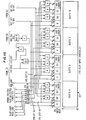
- FIGURE 1 represents a multiprocessing (MP) system containing the described embodiment of the invention. The MP illustrated in FIGURE 1 comprises four central processors, CPO through CP3, in which each CP includes an instruction execution (IE) unit and a buffer control unit (BCE). Each IE includes the hardware and microcode which issue instructions and their storage requests for the fetching and storing of operands in main storage (MS). The IE begins a fetching or storing operation by issuing a fetch or store-interrogate (SI) command to its cache controls (BCE), which includes a processor store-in-cache (SIC) with its associated processor cache directory (PD) and all processor cache controls which are exclusively used by the associated CP. The CP generally issues a fetch or store command for each doubleword (DW) unit required by an operand of an instruction being executed. If the DW is represented in the PD, a cache "hit" occurs for the processor fetch and store command, and the DW is fetched or stored in the associated cache in accordance with the command, whereby the command is completed without any need to go outside of the BCE. Occasionally the required DW is not in the cache, which results in a cache "miss". Before a "missed" fetch or store command can be completed, the line containing the requested DW must be fetched from MS and stored into the cache. To do this, the BCE generates a corresponding "line fetch" command which requests an associated system controller (SC) to obtain from MS the line unit of data having the DW required by the IE. Each line is located in MS on a line boundary, but the required DW will be the first DW in the fetched line to be returned to the requesting BCE.
- In the MP in FIGURE 1, two system controllers SCO and SC1 are each connected to two CPs and to the shared main storage (MS), so that either connected processor can access any shared area in main storage. Each SC also connects I/O to the shared main storage.
- The preferred embodiment includes the subject matter disclosed in prior European Patent applications:
- 79 105 164.2, 80 103 081.8 and 81 107 928.4.
- The shared main storage comprises of a plurality of BSM controllers BSCO through BSC3 in which each BSC connects to two
BSMs - A cross-interrogate (XI) bus connects from each SC to the other SC. The XI bus communicates all cross-interrogation (XI) requests and all castout (CO) and invalidate (INV) signals between the SCs to synchronize and coordinate the required line castout and invalidations in the directories.
- Each SC contains a pair of copy directories. Each copy directory (CD) contains an image of the contents of a corresponding processor cache directory (PD) in one of the BCEs connected to the respective SC.
- The copy directories handle all cross-interrogation (XI) requests, so that the processor cache directories in the various BCEs will not need to handle the XI interrogation requests and can thereby better service their respective CPs. The XI bus connects all SCs and synchronizes all CD searches for conflicts so that searching is avoided in the PDs.
- Each of the other CPs 1-3 has an IE identical to the IEO. Each IE unit is basically similar to IE units found in conventional microprogrammed processors.
- A doubleword wide bidirectional bus is provided between each BSM in main storage (MS) and each SC port, and from each SC to each associated central processor (CP) and I/O channel controller processor (EXDC). Both commands and data may be sent on any bus. The entire system configuration shown in FIGURE 1 is not essential to support the operation of this invention, which is operational with a single SC, its pair of CPs, and at least one BSC with at least one BSM.
- When a CP-cannot find a requested doubleword (DW) in its cache, its buffer control element (BCE), which controls the CP cache, initiates a line access request to MS by sending a miss command to its associated system controller (SC), which then reissues the command to a required BSC and its connected BSM. In the event of a BSM busy condition, the SC will save the request in a command queue and will reissue it at a later time when the required BSM becomes available-. The SC also sequences the MS commands in an orderly fashion, so that all commands to a particular BSM are issued in first-in/first-out (FIFO) order, except when a cache conflict is found. Prior to issuing a MS line the BCE translates the logical (e.g. virtual) address received from the IE into an absolute address which is sent to the SC, and an absolute address to physical address transformation is performed by the SC to determine the BSM location of the requested address. (See European patent application 79 105 164.2.)At the same time in each SC, the request is sent to the storage key array to check for a possible access storage protection violation, and to the copy directories for all CPs to search for a possible data contention conflict. Thus, during the normal sequence of handling a MS request, the SC is constantly monitoring the status of main storage, is analyzing the interrogation results of the storage protect key and all cache directories, is examining the updated status of all pending commands currently being held in the SC, and is also looking for any new BCE commands that may be waiting in the BCE to be received by the SC.
- The main storage protect key arrays are located in the system controller as described in European patent application 80 103 081.8. It performs all key operations defined-by the IBM System/370 architecture. Normally, the storage key and cross-interrogation checking is done in parallel with the issuance of the request to memory and does not interfere with the actual main storage access time when no conflict is detected.
- Due to the store-in-cache (SIC) design of each CP cache, CP changed data resides only in the associated SIC and is not available in MS until the data is castout of the SIC due to an XI request for a changed line, or by the cache slot replacement selection mechanism whenever cache line space is required for newly requested lines. Each SIC has an associated processor cache directory (PD) which controls the SIC operations.
- Because of the nature of each CP store-in-cache (SIC), 'its updated lines are not stored in MS immediately. Thus, many lines of shareable, unchanged and changed data may be scattered among the SICs of the different CPs. Unchanged SIC lines are available in MS, but changed lines are only available in the one SIC in which they reside.
- FIGURE 2 shows the format of the directory entry associated with each line in each SIC, of which the valid (V) bit indicates if the associated line is valid or not.
- The line change (LN CH) bit indicates whether the associated line in SIC is changed or not. The shareability bit (EX) designates the shareability of the associated line as being exclusive in one SIC or as being readonly in plural SICs and is used by the MP cache management controls described and claimed in cited European application 81 107 928.4. The absolute address bits 8-20 in the line entry are part of the absolute main storage address- of the line with bits 19-24 providing the primary congruence class address for each line of sixteen doublewords. The line lock (L) bit is novel to this invention and controls whether the associated line can be invalidated or replaced in the cache when line space is needed in the respective congruence class. The remaining bits in each PD entry are well known and are not pertinent to the subject invention.
- Each CP request for a doubleword (DW) unit is accessed from a line unit of operand data and/or instructions in its cache. Main storage accessing efficiency is greatly improved by having line units of plural DWs (e.g. 16 DWs) accessed as a line fetch unit in MS for each cache, and each cache directory is organized to manage its content on a line basis. Therefore, each PD entry controls a line unit and not a DW unit.
- Any IE may initiate an operand access command to its BCE, such as shown in FIGURE 3, for accessing a doubleword (DW) of data. It is a fetch command if the fetch request bit is on, and it is a store-interrogate (SI) command if the SI bit is on. The store cache signal bit is on only when this command is accompanied by data to be stored in the SIC, and it must be preceeded by a SI command.
- Each CP in the MP generates a sequence of checkpoints which are signalled to its PD by means of the checkpoint signal bit in its IE command to its BCE, shown in FIGURE 3. FIGURE 9 shows the timing of the checkpoint signals provided by the IE. The time between adjacent checkpoints is called a "checkpoint interval", and it may include the execution time for a plurality of instructions in the IE. When the BCE receives any checkpoint signal, it resets all lock (L) bits associated with its SIC. If-an error condition anywhere in the system was sensed in the IE, the IE may issue a retry signal in a command to its BCE which executes a retry operation from the last checkpoint. If the error was temporary, the error will not again occur during the retry, and normal execution will continue.
- After all L bits for any SIC are reset off at any checkpoint, each L bit will continue to remain off until it is set on by a SI command:which either: (1) contains a logical address that compares-equal with the associated SIC line (called a "hit" herein), or (2) the associated slot is selected for replacement by the requested line (called a "miss" herein). This setting on of an L bit is illustrated in FIGURE 9 as occurring during the execution of
instruction 2 in the illustrated example of a checkpoint interval. - The SI command also sets on the change (CH) bit for the addressed slot at the same time that the SI command sets on the L bit. However, the CH bit is not reset when the L bit is reset by a checkpoint signal.
- The occurrence of the next checkpoint ends the current checkpoint interval and resets all L bits. The IE determines when it will issue its next checkpoint signal to that BCE to unlock all locked lines. The IE may hasten a checkpoint signal in response to a cross-interrogation request finding the L bit on for a requested line, and the BCE having the requested locked line issuing a checkpoint request to its IE.
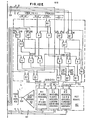
- In FIGURE 8, a congruence class is selected in cache processor directory (PD) 62,
lock array 10, and LRU array 4Z by bits 19-24 from the logical address being requested by"the IE. The congruence class inlock array 10 has a corresponding set of four lock bits respectively representing the four line entries in PD62. Although FIGURE 2 represents the lock bit as effectively part of each PD entry, the implementation shown in FIGURE 8 provides the lock bits separately from the PD array, because it is much faster and more convenient to reset all lock bits simultaneously at each checkpoint when the lock bits are physically together and separated from the PD array which does not have its bits reset by a checkpoint signal. Thus, PD array 62 andlock array 10 each have four columns representing the four slots A, B, C, D in each of 64 congruence classes (i.e. the six bits 19-24 provide 26 = 64 classes). Theconventional LRU array 42 however only has three columns R, S, T which are coded to represent the order of use for the four slots in each congruence class. The settings of the LRU bits R, S, T inarray 10 are determined by the accesses to the slots A, B, C and D in each congruence class, according to the following TABLE 1: -


- The operation of TABLE 1 and TABLE 2 are old in the art, having been disclosed in the previously cited July 1971, IBM Technical Disclosure Bulletin article by Arnold Weinberger.
- However, the next to be described feature involving TABLE 3 is novel to this application, which combines the lock array operation with the LRU operation in a unique manner which excludes each locked slot from being selected,as the LRU slot in the congruence class, even though it may be the least-recently-used slot in its class. This unique feature is represented in FIGURE 8 by the LRU lock selection controls 12, which apply the lock bit settings to the LRU slot values R, S, T to generate a modified LRU selection R', S', T' in any congruence class according to the following TABLE 3:

- To obtain any "modified LRU selection" in TABLE 3, each indicated R, S, or T bit represents the respective valuer for that bit currently being provided from TABLE 2 for an addressed congruence class. The 0 or 1 shown in each "Modified LRU Selection" is caused by the "slots locked" in the class which modifies the LRU slot code to pick a non-locked LRU slot in the addressed congruence class. Thus, the "Slots Locked" column represents all combinations of slots locked for a 4-way set associative cache in which each congruence class has at least one unlocked slot, since all slots may not be locked at one time which would prevent replacement selection in the class.
-
Controls 12 in FIGURE 8 receive the locked slot output signals fromlock array 10 and the RST signals fromLRU array 42 for the addressed class and modify the R, S, T signals into the TABLE 3 R', S', T' signals and translate them into a selection of the unlocked LRU slot A, B, C or D in the addressed class. - For any combination of locked slots, the "Unlocked Slot(s) Aailable" group shown in TABLE 3 indicates a group of slots from which the non-locked LRU slot must be selected. However, at any given time, only one slot is selected from the "Unlocked Slot(s) Available" group due to the specific binary value being provided from TABLE 2 for each R, S, or T bit not predetermined as a 0 or 1 in TABLE 3 for this addressed class. For example, take the third row in TABLE 3 for the C slot locked, which indicates a modified LRU setting of "RST". This means that for a given congruence class (having slots A, B, C and D) that slot C is locked and therefore is not available for replacement. Therefore, the next replacement must be selected from the unlocked slots A, B and D (i.e. the "Unlocked Slot(s) Available" group). However, the conventional LRU controls 42 (which operate according to TABLE 2) may currently indicate any of the eight combinations of R S T represented in TABLE 2, such as for example "1 1 0" indicating slot C as the LRU slot. Thus, if the RST code is 1 1 0 (for C), R is 1 and T is 1 which are put into the R', S', T' code of RST to result in 1 1 1 which determines that slot D is the non-locked LRU slot.
-
Controls 12, in effect, superimpose the lock array settings for the given class upon the general LRU case from TABLE 2 in a mask-like manner to obtain the modified LRU selection (according to TABLE 3 indicated bits R' S' T'). In this example, the "RST" output of TABLE 3 results from locked slot C being combinatorially superimposed on the "1 1 0" indication for slot C from TABLE 2 to generate a "1 1 1" as the R' S' T' value indicating that slot D is the non-locked LRU slot candidate selection. - In order to provide a better understanding of the fundamental operation of this invention, an example of a sequence of fetch and store requests to a cache are illustrated in the following TABLE 4, which illustrates how the LRU states are modified and the effects of a checkpoint (ckpt) operation:

- In summary, the LRU lock selection controls 12 select the non-locked LRU slot as a candidate for the next replacement in any addressed congruence class by eliminating the locked slots from the LRU selection, which is not done by conventional LRU candidate selection (which always chooses the LRU slot from all slots in the class).
- As previously mentioned, this invention prefers that each congruence class have at least one of its four slots unlocked and available for replacement at any time. Whenever three slots become locked in any congruence class, a checkpoint request signal is generated by
controls 12 which is sent to the IE online 153. This allows the IE to make one more SI request to lock the fourth slot in the same class before the IE issues the next checkpoint signal that resets all lock bits for the associated cache but does not disturb the content of PD so that the valid slots continue to remain available for accessing in the cache. - Each-time a processor issues a store-interrogate signal for accessing a doubleword (DW) of data in the store-in-cache,_it causes the existing version of the addressed DW (before it can be changed by a store cache command in a subsequent cycle) to have its cache address stored in a store back address array (SBAA) 17 and have the DW of data stored into a store back data array (SBDA) 16 of the type described in prior cited U.S.A. patent 3,736,566.
- A store back array counter (SBAC) 18 addresses locations in
SBAA 17 andSBDA 16. When reset,SBAC 18 addresseslocation 0 in each. SBAC is incremented by one each time a SI command is received during normal cache operation. At each checkpoint,SBAC 18 is reset to its initial count (0) by the reset signal on line 33. - The SBDA and SBAA store all DWs and their addresses only for SI commands provided by the processor during the same checkpoint interval. In general, SI commands comprise only a small percentage of IE commands, since most commands are for fetch requests.
- The checkpoint interval is controlled by microcode operations in the IE, and a single checkpoint interval gene-rally exists during the execution of N number of instructions by the processor, as shown in FIGURE 9. Each checkpoint requires that the CP complete all outstanding storage requests and not issue any new storage request until the checkpoint operation is completed, the processor operating efficiency is increased by minimizing its number of checkpoints. The processor microcode senses checkpoint requests within the IE and to the IE in order to determine when in the instruction stream to issue the next checkpoint signal. For example, a BCE checkpoint request may be caused by locking the third slot in any congruence class, or by a crossinterrogation request from another processor finding the requested line is locked, or by the
SBAC 18 exceeding a predetermined fill mark. - BCE checkpoint/retry
controls 19 in FIGURE 8 receive each checkpoint signal from the IE. When a checkpoint signal is received, checkpoint controls 19 issue a lock reset signal online 22 to reset all lock bits in thelock array 10 to their unlocked state. The BCE thereby begins the next checkpoint interval with all cache slots being in an unlocked state. - Whenever a retry signal is received by
controls 19 on a line 21 from the IE, controls 19 output a sequence of decrement signals on aline 26 toSBAC counter 18 to cause SBDA 16 to read out its DWs into their original cache locations in the reverse order in which they were received bySBDA 16, untilSBAC 18 reaches its initial count (0). Then the IE can begin a retry operation from the last checkpoint. - The SBDA for example, may hold up to 256 DWs. If no checkpoint is provided, for example, when the 210th DW is received, a
line 27 fromSBAC 18 atcount 210 sends a checkpoint request signal to the IE.SBAC 18 will not be reset to itsinitial setting 0 until the next checkpoint occurs, during which several more storage requests may yet be sent from the IE, and during which the SBDA and SBAA may continue their operation until the current checkpoint interval ends, since they still have space betweenlocations - Therefore any cache miss should never find a fully-locked congruence class in the cache, i.e. in which all slots A, B, C and D have lock bits on, since then no replacement would be permitted in order to maintain retryability, which requires that no cache slot have more than one line during a checkpoint interval, since a second line would overlay the first line and both lines cannto be restored to a single slot for a retry operation. If ever a cache miss is detected in a fully locked congruence class, a machine check error is generated and sent to the IE, and the IE will cause a retry operation from the last checkpoint using the BCE checkpoint retry
controls 19 on line 21. This forces the IE and BCE to retry the CP operations from the last checkpoint, and such error condition will not be permitted to repeat. - Each SC in FIGURE 1 contains a copy of the processor directories in the BCEs directly connected to each SC. These copy directories (CDs) control the inter-CP communication (i.e. cross-interrogation, XI) of CP requests, and the CDs reduce interference with normal SIC operation due to inter-CP communications as explained in cited European application 81 107 928.4.
- The nomenclature used herein distinguishes the issuing CP (which may be any one of CPO-CP3 in the MP issuing a storage request command being XIed) from each of the remote CPs (which are the remaining CPs of CPO-CP3 that did not issue the command for which they are being XIed). The issuing CP and all of its associated entities (i.e. its IE, BCE, PD, SIC and CD) are identified with the suffix (I), i.e. IE(I), BCE (I) , PD(I), SIC(I), and CD(I). Every remote CP and all of its associated entities are identified with the suffix (R), i.e. IE(R), BCE(R), PD(R), SIC(R) and CD(R) .
- A cache miss command (shown in FIGURE 4) occurs if any CP(I) requests a DW which is not found in its PD(I), or is found therein with a readonly (RO) designation when the CP(I) issues a store-interrogate (SI) request which requires that.CD(I) cross-interrogate each CD(R) to find if any other SIC(R) has any copy of the line being requested in order to invalidate remote SIC(R) copies so that SIC(I) can have the line exclusively. The lock bit and the EX bit for the requested line are therefore set on in PD(I), so that this line cannot thereafter be cast out of SIC(I) before the end of the current checkpoint interval. The cross-interrogation (XI) of the copy directories for all SIC(R) in the MP asks the other CPs if they have the requested line and assures the requesting SIC(I) will receive the latest updated version of that line, and invalidates any remote copy of the requested line held unchanged in any SIC(R). ,
- When virtual address bits are used to address the cache directories, they cause potential synonym locations in each directory which must be searched for the absolute address of the CP request as described and claimed in cited European application 81 107 928.4. If a synonym is found in PD(I), the lock bit (L) is set for the synonym location instead of the principle location addressed by the SI request.
- Cross-interrogation (XI) searching is not done in the PD(R)s so that no PD(R) cycles are stolen for XI purposes, and hence almost all PD(R) cycles are available for IE(R) use. Therefore the XI burden is instead placed on the CD (R)s. A PD(R) is only accessed as a result of an XI search of all CD(R)s only when a CD(R) is found to have the requested line. Thus, most XI searches will not access any PD(R), since only a small percentage of XIs will find any line conflict (e.g. less than 5%).
- If a CP(I) store interrogate (SI) command initiated the XI, the command is immediately searched in each CD(R).
- If a readonly conflict is detected in the CD(R), the SC having the conflicting CD(R) issues an invalidate (INV) command to its associated PD(R) to invalidate the conflicting line, since the L bit must be off for a line held RO. Then the PD(R) sends an ILE (invalidate line entry) command to the CD(R) to invalidate the line, which is communicated immediately back to CP(I).
- If an exclusive (EX) conflict is detected, the CD(R) issues a castout (CO) command to its PD(R). Then PD(R) tests its L bit;and if the L bit is off, PD(R) response to the SC command immediately. But if the L bit is on, PD(R) issues a checkpoint request to its IE(R), does not then castout the line, and does not then respond to its SC. The issuing CP(I) then must wait until after the checkpoint (which was requested of IE(R)) before CP(I) can receive the requested data. When the requested checkpoint is shortly thereafter provided by IE(R), then PD(R) responds to SC(R) by issuing a CO (castout) command because the line is held EX and was changed. The PD(R) response to SC(R) is communicated to CP(I) for the XI.
- If a readonly (RO) conflict is detected, the CD(R) issues an invalidate (INV) command to its PD(R), which must have the L,bit off for this RO case. Then PD(R) responds with an tLE command to invalidate the conflicting entry in SC(R).
- If an I/O channel or service processor (SVP) initiates a fetch or store request to main storage, each CD(R) must likewise be cross-interrogated for the address of the request to determine if any SIC has conflicting data. If a conflict is found with a locked line in PD(R), the operations in PD(R) are the same as described for a CP request.
- However, if-a SVP or I/O channel fetch request finds a conflicting line in CD(R) held RO (a RO line cannot be locked), then a different action is taken, which causes the line to be retained by the associated SIC, and no communication is done with the associated PD(R), and therefore no L bit is tested since no castout or invalidation is required.
- To assure the integrity of the XI operation, all copy directories in the MP are searched simultaneously. Therefore, all CD(R)s in the MP are examined for a line address which matches the line address from each CP(I) miss request in the MP. Each CD search operation also detects the presence of any match in all synonym locations for the requested line in every CD. If no match is found in any CD during the search operation, the line fetch request due to the cache miss is immediately accessed in MS. If a match is detected for a synonym in CD(I), the line fetch request is cancelled and the IE access is made in the synonym location in SIC(I). If a match is detected for either the requested address or a synonym address in CD(R), its L bit is tested in PD(R), as previously described.
- Any required castout of an updated line must be made from SIC (R) to MS before its line fetch can be made to SIC(I). Because of this delay for a request with a conflict, it is heM in an SC command queue and is reissued to main storage (MS) when the XI signal is received by SC(I) that the castout line has been stored in MS. The command queues and their SC controls are described and claimed in U.S.A. patent 4,136,386 Filed October 6, 1977 by E. J. Annunziata. The SC connects between MS, the BCEs and the I/O channels by using 72 line bidirectional busses (64 data/command lines plus 8 ECC lines) to provide a doubleword parallel transfer for both the commands are transmitted.
- The reason why CP(I) cannot castout a locked line is because of two architectural rules:(1) a retry from the last checkpoint should obtain the same results as the original execution from the same point in the instruction stream, and (2) an MP architectural rule requires that all CPs in the MP at any particular time must see the same value for the same operand, so that all CPs can generate the same results when using the same operand in a given instruction stream. For example, suppose an operand has a value of "3" in a cache line in CP-A, which CP-A locks and changes to "5" during the same checkpoint interval. Then the original "3" value is put into the store back array for CP-A. Then a retry from the last checkpoint would again be changed to "5".
- However, if the locked value "5" during the same checkpoint interval were then permitted to be castout and replaced by CP-A without a checkpoint, another CP-B in the MP could obtain that operand from main storage and change its value from "5" to "7", for example. If then CP-A were,forced to retry from its last checkpoint, CP-A would again start with the original value "3" for that operand and again change it to the value "5";while at the same time CP-B is using the same operand with a different value of "7", which violates the architectural rule (2) above that all CPs in an MP see the same value for an operand at the same time.
- On the other hand, if CP-A is not allowed to castout the locked value "5", then CP-B cannot get the operand until CP-A resets the lock at the next checkpoint, at which time "3" disappears from the storeback array of CP-A, and this operand with the same value "5".
- Furthermore, if a castout of the locked "5" were permitted, and the "3" in the store back array is overlayed with a "5" for the same line address, the retry capability from the last checkpoint is lost because such retry in CP-A would use "5" instead of "3" with an instruction stream that is retrying from a point where it originally used the value "3", and therefore the retry would not obtain the same results as the original execution which it is suppose to be replacing, which is a violation of architectural rule (1) above that a retry must get the same results as the original execution being retryed.
- The preferred embodiment of the present invention is shown as being implemented in a large data processing system having an architecture associated with the IBM System/370. This architecture is disclosed in the IBM System/370 Principles of Operation" (Form No. GA22-7000-4).
- Pertinent circuits in each BCE are generally shown in a simplified manner in FIGURE 8. The more precise detailed control circuits are shown in FIGURES 10, 11, 12A, B, C, D and E, 13 and 14.
- Whenever any central processor (CP) must either fetch or store a doubleword (DW) of data, the instruction and execution element (IE) in the CP issues the IE command shown in FIGURE 3 to the local buffer control element (BCE) in the CP. The information in the IE command pertinent to the subject invention includes a storage protection key, the logical address of the request, the type of request (i.e. whether it is a fetch request or a store interrogate (SI) request), and whether the data is being requested exclusively (EX) by the CP so that it can store into the data or whether the data is requested non-exclusively (i.e. readonly so that it may be shared on a fetch-only basis among a plurality of processors, none of which is permitted to write into the requested data). The SI request also sets the L bit for the selected cache slot and indicates that an IE store cache command may subsequently be provided to the line when the housekeeping (e.g. translation and/or line fetch) is completed. If no store cache command follows the SI request, the·SI request is handled like a fetch command and the requested DW is fetched and sent to IE. Any subsequent IE store command contains a store cache signal, at which time the IE provides the data on the data-in-bus to the cache to be stored in the cache slot determined by the address in this command. Generally, the IE uses an SI request for a fetch if the fetch is to be followed by other request(s) to the same line which must not be changed by any other processor between those request(s), in order to guarantee an atomic relationship for such sequence of accesses by CP(I).
- FIGURE 7 illustrates how the logical address in the IE command (see FIGURE 3) addresses the processor directory (PD). Bits 19-24 in the address are used to select a row (called a congruence class) in the processor directory (PD) 62. FIGURES 10 and 11 show that each congruence class contains four slots A, B, C and D which are capable 3f representing four respective lines in the associated SIC. In FIGURE 11, the translated address on
line 109 is simultaneously compared with the addresses in each of these four slots which have their valid bits on. If any slot address compares equal, it represents a hit with the requested line. - Approximately 95% of the IE fetch and store requests obtain hits in SIC(I). For the remaining small percentage of the requests which miss in the cache (i.e. no hit), the request cannot be satisfied until that line of data containing the request doubleword is fetched from MS into the SIC(I) of the requesting processor. Before the, line fetch can be made, some important housekeeping functions must be performed. The first is to assure that there is room in the requesting SIC(I) for the requested line, i.e. one or more slots have their invalid bit on. If there is no room, then the least-recently-used (LRU) replacement selection circuits in FIGURE 12B must select which one of the four slot locations in the addressed congruence class is to receive the line to be fetched.
- If the V and CH bits for the line to be replaced indicate a currently valid and changed line exists in that location, that line must be castout to MS before that slot can receive the new line from MS. Also, before the new line can be fetched from main storage, there must be assurance that main storage has the most recently updated version of the new line. This update test is made by cross-interrogating (XIing) all CDs in the MP to determine whether any SIC(R) has a changed version of the line. An updated line possibility is indicated when any CD(R) is found to have the address of the line;and a remote updated line is confirmed if the change (CH) bit is on for that line in the associated remote processor PD(R). The lock (L) bit is also then tested and if on indicates that CP(R) does not want to immediately give up that line to the requesting CP(I).
- Whenever a cache miss occurs in PD(I), the PD(I) slot replacement selection controls shown in FIGURE 12B select an invalid slot, or if there is no invalid slot select the least-recently-used valid slot among the non-locked valid slots in the addressed PD(I) class. That is, if the valid (V) bit is off in any line entry, it may be immediately selected for the new line in the slot order of A, B, C and then
D. Lines lines 131 from FIGURE 12D) is selected. If the CH bit is on in the selected slot, then an updated line currently resides in this slot and it must be castout before the new line can be received by the SIC(I) 63. - Whenever a cache miss is signalled on
line 121 in FIGURE 11, a BCE miss command (shown in FIGURE 4) is generated in BCE(I) and is sent to its SC which makes a request to MS for the line to be fetched, and initiates the XI operations which transmits the miss command (FIGURE 4) to the CD(R)s. The miss command contains the translated absolute address of the requested data, the selected slot position in PD(I) (indicated by activation of one of the four output bits A, B, C or D) from a BCE(I) selectedslot register 132 shown in FIGURE 12B, an OP code field which encodes the line fetch request, a length field which indicates the number of doublewords in the line to be fetched, a SI bit field which indicates whether or not the miss command is a result of a store interrogate request from the IE, and an EX signal field which indicates whether or not the IE requested the data exclusively or readonly. The processor ID field is not transmitted by the BCE but is inserted by the SC when it receives the command, in order for the XI operation to identify the processor from which the command was received, since the XI operations use commands from a number of different processors including from any CP, an I/O processor, or a service processor. - An XIR priority circuit (not shown) in the SC determines when the received command initiates an XI operation by being provided simultaneously on the
XI bus 19 to the other copy directories (CDs) in the system. This initiates a simultaneous search of all copy directories in all SCs --(whether the MP has only a single SC or plural SCs). XI search sync lines connect between plural SCs to synchronize all CD searches in the same machine cycles. The search is for the absolute address of the line for the command currently being searched. Cited European application 81 107 928.4 contains a more detailed description of the XI operations. - Although each CD has an entry for every line found in its corredponding PD, the CD need not have all of the information found in its corresponding PD. This embodiment only requires that each CD include the valid (V) and exclusive-(EX) bits-and high-order absolute address bits 8-20 for each represented line. The entry format found in each PD slot is shown in FIGURE 2 which includes the L bit to accomplish the purposes of this invention by indicating whether or not the corresponding line is locked in the associated SIC.
- In general., each IE sends fetch and store commands (shown in FIGURE 3) to its associated BCE. Instruction fetch requests are requested readonly. IE operand store requests always have the SI request bit on, which also sets the PD entry's L bit in FIGURE 2. For a true store operation, such SI command is followed by another IE command which has the store cache signal field on, and is accompanied by the data being provided by IE(I) to SIC(I). Most IE operand fetch commands have the fetch request bit on. Under special circumstances, this invention enables the SI request bit to be used for a fetch request in order to lock the fetched line so that the IE can obtain a guarantee from the BCE that the fetch request will be atomic with subsequent requests provided by the same IE.
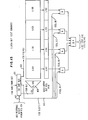
- Whenever a CD(R) finds a conflicting address for a XIed* request command, the SC for that CD(R) sends a command of the type shown in FIGURE 5 to its related PD(R). The SC command signals the detected conflict on
line 160 in FIGURE 14, which sets anSC request trigger 166 in BCE(R). One of the responding BCE(R) operations (which is the response pertinent to this specification) is a test of the state of its L bit for the conflicting line in the lock array local to this BCE(R). This test is done in FIGURE 13 which illustrates the lock bit test circuit found in each BCE, which operates with the lock array outregister 141A in FIGURE 12A which is local to the same CP. The conflicting line's congruence class, and slot in that congruence class, is determined by the CD class and CD slot signals provided in the current SC command (shown in FIGURE 5), which is provided from the SC to register 65 in FIGURE 13. The pertinent lock bit is selected by the one of the select gates actuated by the CD slot signal fromregister 65. If the L bit for the conflicting line in the local (LCL) BCE tests in an on state, an L bit test signal is transmitted online 161 from FIGURE 13 to ANDcircuit 162 in FIGURE 14. - In FIGURE 14, AND
circuit 162 receives its other input from the output of theSC request trigger 166 which indicates when an SC request is provided to this PD(R) as a result of an XI request. Theoutput 163 ofcircuit 162 sets aline hold trigger 164 which remains set while the line is locked in this PD(R). As long astrigger 164 is set, its output viainverter 166 disables an ANDcircuit 167, so that no command request signal can then be provided in this BCE for it to generate a response to the detected conflict (which will be done in FIGURE 15). Theoutput 163 of ANDcircuit 162 also sets a checkpoint request trigger 156 via an ORcircuit 154. When on, the - - output of trigger 156 requests the IE for a checkpoint as soon as the IE is able to provide it, e.g. when it completes its current instruction. - Hence, this CP(R) continues to execute and it decides when it will take its next checkpoint, which is required before (CP(R) can give up the conflicting line. During its execution, this CP(R) may issue requests to its local PD which may hit or miss. If a local (LCL) PD miss occurs, it provides a signal on
line 176 in FIGURE 14 to ANDcircuit 177,whilecircuit 177 is being conditioned by the output of line lockedtrigger 164 indicating the existence of an unresolved conflicting line in this PD(R). The local miss output of ANDcircuit 177 passes through ORcircuit 171 to set theBCE command trigger 172 for one cycle which on line 173A signals its SC that this BCE is sending it a command, and also sends it a con flicting line locked signal through enabled ANDcircuit 173 toline 174 that causes the SC to transmit a con flicting line locked signal to the issuing PD(I). The output oftrigger 172 also passes through OR circuit to reset the line lockedtrigger 164. As a result, the conflict command is erased from BCE(R), and must be later reissued by SC(R). - Accordingly, its SC can begin and complete a line fetch for a miss command from this PD(R) while this PD(R) is awaiting a checkpoint so that it can release a locked line requested by another CP.
- When this IE(R) eventually provides the requested checkpoint, the checkpoint signal is provided on line 157 to reset both the checkpoint trigger 156 and is sent to the SC(R) to cause the SC(R) to reissue the original CP(I) request which has the unresolved conflict. Also in FIGURE 12A, the checkpoint signal on line 157 also resets all the lock bits in the
lock array 141. Thelock array 141 may be constructed of trigger circuits which all have their reset lines connected to checkpoint signal line 157, so that all lock bits inarray 141 are reset simultaneously by each checkpoint signal. A simultaneous checkpoint reset is important in obtaining high performance for large CPs, since it avoids requiring any CP to wait for a sequential reset, which would result from having the lock bits structurally included in a conventional type of cache directory array. - After a checkpoint signal, the lock bits to register 141A in FIGURE 13 will test in an off state, and
line 161 to ANDcircuit 162 in FIGURE 14 is not active and will not set the line lockedtrigger 164 which remains off. - With the lock bit off, the circuit in FIGURE 15 for this PD(R) responds to the conflict caused SC command with a BCE command CO (as shown in FIGURE 6) indicating the requested line is now being castout according to the request of the pending conflict-caused SC command.
- In FIGURE 15, the dropping of the line locked signal on
line 163 causes AND circuits 191-194 to become enabled in accordance to request bits in the pending conflict-signalling SC command in theSC command register 65 in FIGURE 13. The signal from any of AND circuits 191-194 passes through OR circuit 195 to actuate a BCE response reset, which resetsregister 65 and also is provided toline 165 in FIGURE 14 to set theBCE command trigger 172 to signal the SC that it is providing a PD command to the SC. At this time, ANDcircuit 173 is not enabled because the line lockedtrigger 164 had been reset by the previous checkpoint signal. - It is possible for a system deadlock to occur in the MP if two CPs concurrently have conflicts with each other before either can take a checkpoint. Then each CP will be waiting for the other CP to take a next checkpoint, but neither CP can get to its next checkpoint without first receiving the conflicting data from the other CP which cannot be provided. A possible deadlock condition is detected by
circuits - A
line hold trigger 181 is set by a conflicting line locked signal from another CP provided online 184. The other CP provides that signal on itsline 174 via the SC to this CP's trigger 181 (each CP has all of the circuits in-FIGURE 13, 14 and 15 in its local BCE). Thus, trigger 181 is set whenever it receives a signal from any other CP that senses a conflicting locked line. Then if the local CP (i.e. local to this trigger 181) also senses a conflicting locked line by a signal on itslead 163, its AND circuit 182 is enabled and sets itsdeadlock trigger 183, which sends a signal to the SVP for the MP system (see FIGURE 1) that a potential deadlock exists. The relatively slow SVP will respond after a time period which is sufficiently long that if no deadlock exists, one of the two CPs will have taken a checkpoint and broken the deadlock. But if neither CP has then taken a checkpoint, a deadlock is presumed to exist and the SVP forces one of the CPs to retry to its last checkpoint which resets the lock array in that CP and breaks the deadlock. - The lock controlled LRU slot replacement selection circuits shown in FIGURES 12A-E are now discussed in more detail. The
lock array 141 is shown in FIGURE 12A as implemented separately from thePD array 62 in FIGURE 10 or 11, because all lock bits must be reset to off state as a group by each checkpoint signal from the IE. Nevertheless each lock bit inarray 141 is associated with a directory entry in PD62 in the same congruence class and the same slot in the class, so that each PD entry can be considered to logically contain the L bit shown in FIGURE 2. - In FIGURE 12A, the lock bit in one slot in the'addressed class is set by an output from one of the
OR circuits 134 when it receives an input from either ANDcircuits 135 or ANDcircuits 137. One of the ANDcircuits 135 provides an output when a SI request is being provided from the IE via.ANDcircuit 136 and a hit is signalled on one oflines 139. One of ANDcircuits 137 provides an output when a SI request having a cache miss is being provided from the one of ANDcircuits 137 that is being enabled by the one of thelines 133 representing the slot being replaced. - The circuits in FIGURE 12C detect when a third slot is locked in the addressed congruence class. The currently locked slots in the class are indicated by the
lines 142 fromlock array 141. The six ANDcircuits 151 represent all combinations of any two slots currently locked in the addressed class. Whenever any third slot is locked in the class, a checkpoint request trigger 156 is set byline 153, and then outputs a checkpoint request signal which is sent to the associated IE. An output from any of the six ANDcircuits 151 passes through an OR circuit to condition an ANDcircuit 152. However, trigger 156 is not set until ANDcircuit 152 is activated by an SI access signal from any of the four ORcircuits 134 in FIGURE 12A which is about to lock the third slot in the addressed class. Note that during the cycle in which the second slot is locked, that the lock array is only outputting one locked slot, so that none of ANDcircuits 151 is then activated when that SI access signal conditions the other input to ANDcircuit 152, which thereby remains disabled during the locking of the second slot in any class. - FIGURE 12E contains a conventional LRU replacement selection circuit of the type disclosed in the cited 1971 article to A. Weinberger. The
RST output lines 161 provide the codes shown in TABLE 2, previously included and discussed in tbis specification. The RST array comprises three separate array circuits R, S and T which respectively contain;the R, S, and T values for all congruence classes. - The'three array circuits are addressed by the same
class address decoder 163 which receives the PD congruence class address bits 19-24 onbus 108 from the PD address register in FIGURE 7. Each of array circuits R, S and T has two inputs, I and W. The W input must be active in order to write anything into the array bit in the currently addressed congruence class. The W input is active on any access -(i.e hit or miss with replacement) which sets a value into the array circuit indicated in TABLE 1 herein. - The I input then controls whether the zero (0) or one (1) bit value is written. When the W input is not active, the addressed array bit is not changed in accordance with TABLE 1.
- Thus, in the R array circuit, its W input is activated on every slot access (i.e. A or B or C or D access) while its I input writes a 1 bit if the A or B slot is accessed, or writes a 0 bit if the C or D slot is accessed. The W input of the S array circuit is active only for A or B slot accesses, while the I input writes a 1 bit during the A slot access and a 0 bit during the B slot access.
- The W input of the T array circuit is active only for a C or D slot access, while its I input writes a 1 bit for the C slot access and a 0 bit for the D slot access.
- R', S', T'
circuits 171 in FIGURE 12D receive theRST lines 161 from FIGURE 12E (via FIGURE 12B), and also receive the ABCD lockarray output lines 142 from FIGURE 12A (via FIGURE 12C) to perform the invented function (previously described in regard to TABLE 3 herein) of eliminating the locked slot(s) from every replacement choice and then selecting the replacement slot as the LRU slot among the remaining non-locked slots. The non-locked LRU slot replacement selection for an addressed congruence class is indicated by the R'S'T' signals outputted fromcircuits 171 tocircuits 181. -
Circuits 181 in FIGURE 12D translate the three received R'S'T' combinatorial signals into one of the four signals A, B, C or D in the lines ofbus 131 to represent the non-locked LRU slot currently available for replacement in the addressed class. The available non-locked LRU slot signal inbus 131 is provided to FIGURE 12B as an input to the slot selection circuits in FIGURE 12B, which make the final slot selection for the addressed class and sets each final selection into the selectedslot register 132. If any invalid slot exists, it will be chosen for replacement by the circuits in FIGURE 12B instead of any valid LRU slot indicated by the signals onbus 131. Thus, the non-locked LRU slot outputted from FIGURE 12D is only selected for replacement when all slots A, B, C and D are valid in the addressed class.
Claims (10)
characterized in that a lock bit (L) is provided in the cache directory entry for each cache line, that the lock bit is set under processor control and that for line replacement the lock bits are evaluated to select only unlocked lines in each set- _ associative congruence class within the cache.

characterized in that the lock bit (L) of a cache line is set by a processor instruction (S1) initi- ating a cache fetch or store operation.
characterized in that the execution of a checkpoint operation is requested whenever all lines in any congruence class have become locked.
characterized in that locked lines detected in the cache of another processor in the multiprocessor system during a cross-interrogation operation are blocked from being castout or invalidated until their lock bit is turned off at a next checkpoint.
characterized in that the lock bit is set by the processor in storage operations requiring independence of other processors in instruction execution (ato- micity).
characterized in that a potential deadlock signal is generated (circuits 181-183, Fig. 14) and transferred to system control circuits (SUP) whenever two processors detect concurrent conflicting locked lines.
characterized in that the cache directory (PD) entry for each cache line contains an Ex-bit, designating the line as exclusively reserved for the associated processor.
Applications Claiming Priority (2)
| Application Number | Priority Date | Filing Date | Title |
|---|---|---|---|
| US06/246,788 US4513367A (en) | 1981-03-23 | 1981-03-23 | Cache locking controls in a multiprocessor |
| US246788 | 1994-05-19 |
Publications (3)
| Publication Number | Publication Date |
|---|---|
| EP0061570A2 true EP0061570A2 (en) | 1982-10-06 |
| EP0061570A3 EP0061570A3 (en) | 1984-07-18 |
| EP0061570B1 EP0061570B1 (en) | 1988-08-10 |
Family
ID=22932207
Family Applications (1)
| Application Number | Title | Priority Date | Filing Date |
|---|---|---|---|
| EP82100836A Expired EP0061570B1 (en) | 1981-03-23 | 1982-02-05 | Store-in-cache multiprocessor system with checkpoint feature |
Country Status (4)
| Country | Link |
|---|---|
| US (1) | US4513367A (en) |
| EP (1) | EP0061570B1 (en) |
| JP (1) | JPS57158081A (en) |
| DE (1) | DE3278890D1 (en) |
Cited By (20)
| Publication number | Priority date | Publication date | Assignee | Title |
|---|---|---|---|---|
| EP0144763A2 (en) * | 1983-12-12 | 1985-06-19 | International Business Machines Corporation | Address translation apparatus for a virtual memory data processing system |
| EP0381325A2 (en) * | 1989-02-03 | 1990-08-08 | Digital Equipment Corporation | Synchronising and processing of memory access operations |
| EP0568221A1 (en) * | 1992-04-29 | 1993-11-03 | Sun Microsystems, Inc. | Methods and apparatus for implementing a pseudo-LRU cache memory replacement scheme with a locking feature |
| DE4407626C1 (en) * | 1994-03-08 | 1995-05-24 | Karl Michael Marks | Process for control of cache buffers in data processing system |
| EP0768608A2 (en) * | 1995-10-13 | 1997-04-16 | Sun Microsystems, Inc. | Maximal concurrent lookup cache for computing systems having a multi-threaded environment |
| WO1998002818A1 (en) * | 1996-07-16 | 1998-01-22 | Advanced Micro Devices, Inc. | A data memory unit configured to store data in one clock cycle and method for operating same |
| US5761712A (en) * | 1995-06-07 | 1998-06-02 | Advanced Micro Devices | Data memory unit and method for storing data into a lockable cache in one clock cycle by previewing the tag array |
| US5893140A (en) * | 1996-08-14 | 1999-04-06 | Emc Corporation | File server having a file system cache and protocol for truly safe asynchronous writes |
| US5892915A (en) * | 1997-04-25 | 1999-04-06 | Emc Corporation | System having client sending edit commands to server during transmission of continuous media from one clip in play list for editing the play list |
| US5948062A (en) * | 1995-10-27 | 1999-09-07 | Emc Corporation | Network file server using a cached disk array storing a network file directory including file locking information and data mover computers each having file system software for shared read-write file access |
| US5974503A (en) * | 1997-04-25 | 1999-10-26 | Emc Corporation | Storage and access of continuous media files indexed as lists of raid stripe sets associated with file names |
| US5987621A (en) * | 1997-04-25 | 1999-11-16 | Emc Corporation | Hardware and software failover services for a file server |
| US6061504A (en) * | 1995-10-27 | 2000-05-09 | Emc Corporation | Video file server using an integrated cached disk array and stream server computers |
| US6298386B1 (en) | 1996-08-14 | 2001-10-02 | Emc Corporation | Network file server having a message collector queue for connection and connectionless oriented protocols |
| CN1093962C (en) * | 1996-12-24 | 2002-11-06 | 国际商业机器公司 | Improved high-speed buffer storage system |
| US6732234B1 (en) | 2000-08-07 | 2004-05-04 | Broadcom Corporation | Direct access mode for a cache |
| US6748492B1 (en) | 2000-08-07 | 2004-06-08 | Broadcom Corporation | Deterministic setting of replacement policy in a cache through way selection |
| US6748495B2 (en) | 2001-05-15 | 2004-06-08 | Broadcom Corporation | Random generator |
| US6848024B1 (en) | 2000-08-07 | 2005-01-25 | Broadcom Corporation | Programmably disabling one or more cache entries |
| US6988168B2 (en) | 2002-05-15 | 2006-01-17 | Broadcom Corporation | Cache programmable to partition ways to agents and/or local/remote blocks |
Families Citing this family (85)
| Publication number | Priority date | Publication date | Assignee | Title |
|---|---|---|---|---|
| US4714990A (en) * | 1982-09-18 | 1987-12-22 | International Computers Limited | Data storage apparatus |
| JPH0658646B2 (en) | 1982-12-30 | 1994-08-03 | インタ−ナショナル・ビジネス・マシ−ンズ・コ−ポレ−ション | Virtual memory address translation mechanism with controlled data persistence |
| US4648030A (en) * | 1983-09-22 | 1987-03-03 | Digital Equipment Corporation | Cache invalidation mechanism for multiprocessor systems |
| DE3566314D1 (en) * | 1984-04-26 | 1988-12-22 | Bbc Brown Boveri & Cie | Apparatus for saving a calculator status |
| US4638431A (en) * | 1984-09-17 | 1987-01-20 | Nec Corporation | Data processing system for vector processing having a cache invalidation control unit |
| EP0194024B1 (en) * | 1985-02-05 | 1992-09-09 | Digital Equipment Corporation | Apparatus and method for controlling access in a multi-cache data processing system |
| US4821171A (en) * | 1985-05-07 | 1989-04-11 | Prime Computer, Inc. | System of selective purging of address translation in computer memories |
| US4775955A (en) * | 1985-10-30 | 1988-10-04 | International Business Machines Corporation | Cache coherence mechanism based on locking |
| US5029072A (en) * | 1985-12-23 | 1991-07-02 | Motorola, Inc. | Lock warning mechanism for a cache |
| US4885680A (en) * | 1986-07-25 | 1989-12-05 | International Business Machines Corporation | Method and apparatus for efficiently handling temporarily cacheable data |
| US5317717A (en) * | 1987-07-01 | 1994-05-31 | Digital Equipment Corp. | Apparatus and method for main memory unit protection using access and fault logic signals |
| US5291581A (en) * | 1987-07-01 | 1994-03-01 | Digital Equipment Corporation | Apparatus and method for synchronization of access to main memory signal groups in a multiprocessor data processing system |
| US4910656A (en) * | 1987-09-21 | 1990-03-20 | Motorola, Inc. | Bus master having selective burst initiation |
| US5025366A (en) * | 1988-01-20 | 1991-06-18 | Advanced Micro Devices, Inc. | Organization of an integrated cache unit for flexible usage in cache system design |
| ATE109910T1 (en) * | 1988-01-20 | 1994-08-15 | Advanced Micro Devices Inc | ORGANIZATION OF AN INTEGRATED CACHE FOR FLEXIBLE APPLICATION TO SUPPORT MULTIPROCESSOR OPERATIONS. |
| US5136691A (en) * | 1988-01-20 | 1992-08-04 | Advanced Micro Devices, Inc. | Methods and apparatus for caching interlock variables in an integrated cache memory |
| US4977498A (en) * | 1988-04-01 | 1990-12-11 | Digital Equipment Corporation | Data processing system having a data memory interlock coherency scheme |
| US5003459A (en) * | 1988-04-01 | 1991-03-26 | Digital Equipment Corporation | Cache memory system |
| US4912630A (en) * | 1988-07-29 | 1990-03-27 | Ncr Corporation | Cache address comparator with sram having burst addressing control |
| US5317716A (en) * | 1988-08-16 | 1994-05-31 | International Business Machines Corporation | Multiple caches using state information indicating if cache line was previously modified and type of access rights granted to assign access rights to cache line |
| US5175861A (en) * | 1988-10-14 | 1992-12-29 | Nec Corporation | Lock processing system |
| US5210848A (en) * | 1989-02-22 | 1993-05-11 | International Business Machines Corporation | Multi-processor caches with large granularity exclusivity locking |
| US5060144A (en) * | 1989-03-16 | 1991-10-22 | Unisys Corporation | Locking control with validity status indication for a multi-host processor system that utilizes a record lock processor and a cache memory for each host processor |
| US5230070A (en) * | 1989-09-08 | 1993-07-20 | International Business Machines Corporation | Access authorization table for multi-processor caches |
| US7610452B1 (en) * | 1989-10-31 | 2009-10-27 | Canon Kabushiki Kaisha | Data processing system wherein data is stored in a memory and an external storage in parallel |
| JPH0786848B2 (en) * | 1989-11-01 | 1995-09-20 | 三菱電機株式会社 | Cache memory |
| US5226143A (en) * | 1990-03-14 | 1993-07-06 | International Business Machines Corporation | Multiprocessor system includes operating system for notifying only those cache managers who are holders of shared locks on a designated page by global lock manager |
| US5197139A (en) * | 1990-04-05 | 1993-03-23 | International Business Machines Corporation | Cache management for multi-processor systems utilizing bulk cross-invalidate |
| US5249286A (en) * | 1990-05-29 | 1993-09-28 | National Semiconductor Corporation | Selectively locking memory locations within a microprocessor's on-chip cache |
| JP2511588B2 (en) * | 1990-09-03 | 1996-06-26 | インターナショナル・ビジネス・マシーンズ・コーポレイション | Data processing network, method for acquiring lock and serialization device |
| US5269009A (en) * | 1990-09-04 | 1993-12-07 | International Business Machines Corporation | Processor system with improved memory transfer means |
| US5339397A (en) * | 1990-10-12 | 1994-08-16 | International Business Machines Corporation | Hardware primary directory lock |
| JP2743608B2 (en) * | 1991-03-27 | 1998-04-22 | 日本電気株式会社 | Shared register control method |
| JPH04364515A (en) * | 1991-06-11 | 1992-12-16 | Hitachi Ltd | Recording medium reproduction device |
| GB9118312D0 (en) * | 1991-08-24 | 1991-10-09 | Motorola Inc | Real time cache implemented by dual purpose on-chip memory |
| EP0529303A3 (en) * | 1991-08-29 | 1993-09-22 | International Business Machines Corporation | Checkpoint synchronization with instruction overlap enabled |
| US5974508A (en) * | 1992-07-31 | 1999-10-26 | Fujitsu Limited | Cache memory system and method for automatically locking cache entries to prevent selected memory items from being replaced |
| US5493667A (en) * | 1993-02-09 | 1996-02-20 | Intel Corporation | Apparatus and method for an instruction cache locking scheme |
| JPH06243036A (en) * | 1993-02-12 | 1994-09-02 | Hitachi Ltd | Cache control system |
| JP3230898B2 (en) * | 1993-06-02 | 2001-11-19 | シャープ株式会社 | Data driven information processing system |
| JPH06348595A (en) * | 1993-06-07 | 1994-12-22 | Hitachi Ltd | Cache device |
| US6006299A (en) * | 1994-03-01 | 1999-12-21 | Intel Corporation | Apparatus and method for caching lock conditions in a multi-processor system |
| US5655103A (en) * | 1995-02-13 | 1997-08-05 | International Business Machines Corporation | System and method for handling stale data in a multiprocessor system |
| JP3086779B2 (en) * | 1995-06-19 | 2000-09-11 | 株式会社東芝 | Memory state restoration device |
| US5832291A (en) * | 1995-12-15 | 1998-11-03 | Raytheon Company | Data processor with dynamic and selectable interconnections between processor array, external memory and I/O ports |
| US5787486A (en) * | 1995-12-15 | 1998-07-28 | International Business Machines Corporation | Bus protocol for locked cycle cache hit |
| US5875462A (en) * | 1995-12-28 | 1999-02-23 | Unisys Corporation | Multi-processor data processing system with multiple second level caches mapable to all of addressable memory |
| US5822764A (en) * | 1996-03-04 | 1998-10-13 | Motorola, Inc. | Method and circuit for efficiently replacing invalid locked portions of a cache with valid data |
| TW379298B (en) * | 1996-09-30 | 2000-01-11 | Toshiba Corp | Memory updating history saving device and memory updating history saving method |
| US6175899B1 (en) * | 1997-05-19 | 2001-01-16 | International Business Machines Corporation | Method for providing virtual atomicity in multi processor environment having access to multilevel caches |
| US6044478A (en) * | 1997-05-30 | 2000-03-28 | National Semiconductor Corporation | Cache with finely granular locked-down regions |
| US6047358A (en) * | 1997-10-31 | 2000-04-04 | Philips Electronics North America Corporation | Computer system, cache memory and process for cache entry replacement with selective locking of elements in different ways and groups |
| US6141734A (en) * | 1998-02-03 | 2000-10-31 | Compaq Computer Corporation | Method and apparatus for optimizing the performance of LDxL and STxC interlock instructions in the context of a write invalidate protocol |
| JP2000200221A (en) * | 1998-10-30 | 2000-07-18 | Nec Corp | Cache memory device and its control method |
| GB2385174B (en) | 1999-01-19 | 2003-11-26 | Advanced Risc Mach Ltd | Memory control within data processing systems |
| US6560677B1 (en) | 1999-05-04 | 2003-05-06 | International Business Machines Corporation | Methods, cache memories, systems and computer program products for storing transient, normal, and locked entries in an associative cache memory |
| US6785714B1 (en) * | 2000-09-28 | 2004-08-31 | Microsoft Corporation | System and method for employing slot level locking of a cache |
| US7234027B2 (en) * | 2001-10-24 | 2007-06-19 | Cray Inc. | Instructions for test & set with selectively enabled cache invalidate |
| US7162608B2 (en) * | 2001-10-24 | 2007-01-09 | Cray, Inc. | Translation lookaside buffer-based memory system and method for use in a computer having a plurality of processor element |
| US7107410B2 (en) * | 2003-01-07 | 2006-09-12 | Hewlett-Packard Development Company, L.P. | Exclusive status tags |
| JP4376692B2 (en) * | 2004-04-30 | 2009-12-02 | 富士通株式会社 | Information processing device, processor, processor control method, information processing device control method, cache memory |
| US7321954B2 (en) * | 2004-08-11 | 2008-01-22 | International Business Machines Corporation | Method for software controllable dynamically lockable cache line replacement system |
| US20060179231A1 (en) * | 2005-02-07 | 2006-08-10 | Advanced Micron Devices, Inc. | System having cache memory and method of accessing |
| US7930484B2 (en) * | 2005-02-07 | 2011-04-19 | Advanced Micro Devices, Inc. | System for restricted cache access during data transfers and method thereof |
| US8131936B2 (en) * | 2005-02-11 | 2012-03-06 | International Business Machines Corporation | Method and apparatus for implementing a combined data/coherency cache |
| US8606998B2 (en) * | 2006-08-24 | 2013-12-10 | Advanced Micro Devices, Inc. | System and method for instruction-based cache allocation policies |
| US7590899B2 (en) * | 2006-09-15 | 2009-09-15 | International Business Machines Corporation | Processor memory array having memory macros for relocatable store protect keys |
| US20080147989A1 (en) * | 2006-12-14 | 2008-06-19 | Arm Limited | Lockdown control of a multi-way set associative cache memory |
| US8051338B2 (en) * | 2007-07-19 | 2011-11-01 | Cray Inc. | Inter-asic data transport using link control block manager |
| US7827360B2 (en) * | 2007-08-02 | 2010-11-02 | Freescale Semiconductor, Inc. | Cache locking device and methods thereof |
| US9396227B2 (en) * | 2012-03-29 | 2016-07-19 | Hewlett Packard Enterprise Development Lp | Controlled lock violation for data transactions |
| US9003125B2 (en) * | 2012-06-14 | 2015-04-07 | International Business Machines Corporation | Cache coherency protocol for allowing parallel data fetches and eviction to the same addressable index |
| US9298469B2 (en) | 2012-06-15 | 2016-03-29 | International Business Machines Corporation | Management of multiple nested transactions |
| US9262320B2 (en) | 2012-06-15 | 2016-02-16 | International Business Machines Corporation | Tracking transactional execution footprint |
| US9015419B2 (en) * | 2012-06-15 | 2015-04-21 | International Business Machines Corporation | Avoiding aborts due to associativity conflicts in a transactional environment |
| US9223687B2 (en) | 2012-06-15 | 2015-12-29 | International Business Machines Corporation | Determining the logical address of a transaction abort |
| US9298631B2 (en) | 2012-06-15 | 2016-03-29 | International Business Machines Corporation | Managing transactional and non-transactional store observability |
| US9311101B2 (en) | 2012-06-15 | 2016-04-12 | International Business Machines Corporation | Intra-instructional transaction abort handling |
| CN103885892A (en) * | 2012-12-20 | 2014-06-25 | 株式会社东芝 | Memory controller |
| US10089025B1 (en) | 2016-06-29 | 2018-10-02 | EMC IP Holding Company LLC | Bloom filters in a flash memory |
| US10037164B1 (en) | 2016-06-29 | 2018-07-31 | EMC IP Holding Company LLC | Flash interface for processing datasets |
| US10146438B1 (en) | 2016-06-29 | 2018-12-04 | EMC IP Holding Company LLC | Additive library for data structures in a flash memory |
| US10055351B1 (en) | 2016-06-29 | 2018-08-21 | EMC IP Holding Company LLC | Low-overhead index for a flash cache |
| US10331561B1 (en) | 2016-06-29 | 2019-06-25 | Emc Corporation | Systems and methods for rebuilding a cache index |
| US10261704B1 (en) | 2016-06-29 | 2019-04-16 | EMC IP Holding Company LLC | Linked lists in flash memory |
Citations (3)
| Publication number | Priority date | Publication date | Assignee | Title |
|---|---|---|---|---|
| US3735360A (en) * | 1971-08-25 | 1973-05-22 | Ibm | High speed buffer operation in a multi-processing system |
| US3736566A (en) * | 1971-08-18 | 1973-05-29 | Ibm | Central processing unit with hardware controlled checkpoint and retry facilities |
| EP0009412A2 (en) * | 1978-09-25 | 1980-04-02 | Sperry Corporation | Block replacement in a high speed cache memory system |
Family Cites Families (12)
| Publication number | Priority date | Publication date | Assignee | Title |
|---|---|---|---|---|
| US3533082A (en) * | 1968-01-15 | 1970-10-06 | Ibm | Instruction retry apparatus including means for restoring the original contents of altered source operands |
| US3533065A (en) * | 1968-01-15 | 1970-10-06 | Ibm | Data processing system execution retry control |
| US3564506A (en) * | 1968-01-17 | 1971-02-16 | Ibm | Instruction retry byte counter |
| GB1509193A (en) * | 1974-04-17 | 1978-05-04 | Nat Res Dev | Computer systems |
| US4077059A (en) * | 1975-12-18 | 1978-02-28 | Cordi Vincent A | Multi-processing system with a hierarchial memory having journaling and copyback |
| US4084230A (en) * | 1976-11-29 | 1978-04-11 | International Business Machines Corporation | Hybrid semiconductor memory with on-chip associative page addressing, page replacement and control |
| US4136386A (en) * | 1977-10-06 | 1979-01-23 | International Business Machines Corporation | Backing store access coordination in a multi-processor system |
| US4195340A (en) * | 1977-12-22 | 1980-03-25 | Honeywell Information Systems Inc. | First in first out activity queue for a cache store |
| US4195341A (en) * | 1977-12-22 | 1980-03-25 | Honeywell Information Systems Inc. | Initialization of cache store to assure valid data |
| US4387427A (en) * | 1978-12-21 | 1983-06-07 | Intel Corporation | Hardware scheduler/dispatcher for data processing system |
| US4293910A (en) * | 1979-07-02 | 1981-10-06 | International Business Machines Corporation | Reconfigurable key-in-storage means for protecting interleaved main storage |
| US4317168A (en) * | 1979-11-23 | 1982-02-23 | International Business Machines Corporation | Cache organization enabling concurrent line castout and line fetch transfers with main storage |
-
1981
- 1981-03-23 US US06/246,788 patent/US4513367A/en not_active Expired - Fee Related
-
1982
- 1982-01-20 JP JP57006201A patent/JPS57158081A/en active Granted
- 1982-02-05 EP EP82100836A patent/EP0061570B1/en not_active Expired
- 1982-02-05 DE DE8282100836T patent/DE3278890D1/en not_active Expired
Patent Citations (3)
| Publication number | Priority date | Publication date | Assignee | Title |
|---|---|---|---|---|
| US3736566A (en) * | 1971-08-18 | 1973-05-29 | Ibm | Central processing unit with hardware controlled checkpoint and retry facilities |
| US3735360A (en) * | 1971-08-25 | 1973-05-22 | Ibm | High speed buffer operation in a multi-processing system |
| EP0009412A2 (en) * | 1978-09-25 | 1980-04-02 | Sperry Corporation | Block replacement in a high speed cache memory system |
Non-Patent Citations (4)
| Title |
|---|
| IBM TECHNICAL DISCLOSURE BULLETIN, vol. 14, no. 2, July 1971, pages 430-432, New York, USA * |
| IBM TECHNICAL DISCLOSURE BULLETIN, vol. 21, no. 1, June 1978, pages 280-281, New York, USA * |
| IBM TECHNICAL DISCLOSURE BULLETIN, vol. 21, no. 6, November 1978, page 2290, New York, USA * |
| IBM TECHNICAL DISCLOSURE BULLETIN, vol. 22, no. 6, November 1979, pages 2317-2318, New York, USA * |
Cited By (30)
| Publication number | Priority date | Publication date | Assignee | Title |
|---|---|---|---|---|
| EP0144763A2 (en) * | 1983-12-12 | 1985-06-19 | International Business Machines Corporation | Address translation apparatus for a virtual memory data processing system |
| EP0144763A3 (en) * | 1983-12-12 | 1988-03-30 | International Business Machines Corporation | Address translation apparatus for a virtual memory data processing system |
| EP0381325A2 (en) * | 1989-02-03 | 1990-08-08 | Digital Equipment Corporation | Synchronising and processing of memory access operations |
| EP0381325A3 (en) * | 1989-02-03 | 1992-06-03 | Digital Equipment Corporation | Synchronising and processing of memory access operations |
| US5175837A (en) * | 1989-02-03 | 1992-12-29 | Digital Equipment Corporation | Synchronizing and processing of memory access operations in multiprocessor systems using a directory of lock bits |
| EP0568221A1 (en) * | 1992-04-29 | 1993-11-03 | Sun Microsystems, Inc. | Methods and apparatus for implementing a pseudo-LRU cache memory replacement scheme with a locking feature |
| US5353425A (en) * | 1992-04-29 | 1994-10-04 | Sun Microsystems, Inc. | Methods and apparatus for implementing a pseudo-LRU cache memory replacement scheme with a locking feature |
| DE4407626C1 (en) * | 1994-03-08 | 1995-05-24 | Karl Michael Marks | Process for control of cache buffers in data processing system |
| US5761712A (en) * | 1995-06-07 | 1998-06-02 | Advanced Micro Devices | Data memory unit and method for storing data into a lockable cache in one clock cycle by previewing the tag array |
| EP0768608A2 (en) * | 1995-10-13 | 1997-04-16 | Sun Microsystems, Inc. | Maximal concurrent lookup cache for computing systems having a multi-threaded environment |
| CN1087451C (en) * | 1995-10-13 | 2002-07-10 | 太阳微系统有限公司 | Maximum concurrent-searching high-speed buffering storage unit for computor system with multiple thread environment |
| EP0768608A3 (en) * | 1995-10-13 | 1998-08-12 | Sun Microsystems, Inc. | Maximal concurrent lookup cache for computing systems having a multi-threaded environment |
| US5948062A (en) * | 1995-10-27 | 1999-09-07 | Emc Corporation | Network file server using a cached disk array storing a network file directory including file locking information and data mover computers each having file system software for shared read-write file access |
| US6061504A (en) * | 1995-10-27 | 2000-05-09 | Emc Corporation | Video file server using an integrated cached disk array and stream server computers |
| WO1998002818A1 (en) * | 1996-07-16 | 1998-01-22 | Advanced Micro Devices, Inc. | A data memory unit configured to store data in one clock cycle and method for operating same |
| US5893140A (en) * | 1996-08-14 | 1999-04-06 | Emc Corporation | File server having a file system cache and protocol for truly safe asynchronous writes |
| US6298386B1 (en) | 1996-08-14 | 2001-10-02 | Emc Corporation | Network file server having a message collector queue for connection and connectionless oriented protocols |
| CN1093962C (en) * | 1996-12-24 | 2002-11-06 | 国际商业机器公司 | Improved high-speed buffer storage system |
| US5892915A (en) * | 1997-04-25 | 1999-04-06 | Emc Corporation | System having client sending edit commands to server during transmission of continuous media from one clip in play list for editing the play list |
| US5974503A (en) * | 1997-04-25 | 1999-10-26 | Emc Corporation | Storage and access of continuous media files indexed as lists of raid stripe sets associated with file names |
| US5987621A (en) * | 1997-04-25 | 1999-11-16 | Emc Corporation | Hardware and software failover services for a file server |
| US6732234B1 (en) | 2000-08-07 | 2004-05-04 | Broadcom Corporation | Direct access mode for a cache |
| US6748492B1 (en) | 2000-08-07 | 2004-06-08 | Broadcom Corporation | Deterministic setting of replacement policy in a cache through way selection |
| US6848024B1 (en) | 2000-08-07 | 2005-01-25 | Broadcom Corporation | Programmably disabling one or more cache entries |
| US6961824B2 (en) | 2000-08-07 | 2005-11-01 | Broadcom Corporation | Deterministic setting of replacement policy in a cache |
| US7177986B2 (en) | 2000-08-07 | 2007-02-13 | Broadcom Corporation | Direct access mode for a cache |
| US7228386B2 (en) | 2000-08-07 | 2007-06-05 | Broadcom Corporation | Programmably disabling one or more cache entries |
| US6748495B2 (en) | 2001-05-15 | 2004-06-08 | Broadcom Corporation | Random generator |
| US7000076B2 (en) | 2001-05-15 | 2006-02-14 | Broadcom Corporation | Random generator |
| US6988168B2 (en) | 2002-05-15 | 2006-01-17 | Broadcom Corporation | Cache programmable to partition ways to agents and/or local/remote blocks |
Also Published As
| Publication number | Publication date |
|---|---|
| EP0061570A3 (en) | 1984-07-18 |
| EP0061570B1 (en) | 1988-08-10 |
| US4513367A (en) | 1985-04-23 |
| JPS57158081A (en) | 1982-09-29 |
| DE3278890D1 (en) | 1988-09-22 |
| JPS612975B2 (en) | 1986-01-29 |
Similar Documents
| Publication | Publication Date | Title |
|---|---|---|
| EP0061570B1 (en) | Store-in-cache multiprocessor system with checkpoint feature | |
| US4400770A (en) | Cache synonym detection and handling means | |
| US4394731A (en) | Cache storage line shareability control for a multiprocessor system | |
| US5490261A (en) | Interlock for controlling processor ownership of pipelined data for a store in cache | |
| EP0422113B1 (en) | Multi-processor system with cache memories | |
| US4399506A (en) | Store-in-cache processor means for clearing main storage | |
| US4484267A (en) | Cache sharing control in a multiprocessor | |
| EP0095598B1 (en) | Multiprocessor with independent direct cache-to-cache data transfers | |
| US5875472A (en) | Address conflict detection system employing address indirection for use in a high-speed multi-processor system | |
| US5696937A (en) | Cache controller utilizing a state machine for controlling invalidations in a network with dual system busses | |
| US6249846B1 (en) | Distributed data dependency stall mechanism | |
| EP0507063A1 (en) | Cross-invalidate directory method and means | |
| EP0372201B1 (en) | Method for fetching potentially dirty data in multiprocessor systems | |
| US5845324A (en) | Dual bus network cache controller system having rapid invalidation cycles and reduced latency for cache access | |
| US4410946A (en) | Cache extension to processor local storage | |
| JPH0743670B2 (en) | Store-through cache management system | |
| US6105108A (en) | Method and apparatus for releasing victim data buffers of computer systems by comparing a probe counter with a service counter | |
| US5269009A (en) | Processor system with improved memory transfer means | |
| US6061765A (en) | Independent victim data buffer and probe buffer release control utilzing control flag | |
| EP0212678B1 (en) | Cache storage synonym detection and handling means | |
| US5016168A (en) | Method for storing into non-exclusive cache lines in multiprocessor systems | |
| US5737756A (en) | Dual bus computer network using dual busses with dual spy modules enabling clearing of invalidation queue for processor with store through cache while providing retry cycles for incomplete accesses to invalidation queue | |
| JP2001222468A (en) | Load/store instruction control circuit in microprocessor and method for controlling load/store instruction | |
| EP1725938A1 (en) | System and method for canceling write back operation during simultaneous snoop push or snoop kill operation in write back caches | |
| JPH0574101B2 (en) |
Legal Events
| Date | Code | Title | Description |
|---|---|---|---|
| PUAI | Public reference made under article 153(3) epc to a published international application that has entered the european phase |
Free format text: ORIGINAL CODE: 0009012 |
|
| AK | Designated contracting states |
Designated state(s): DE FR GB |
|
| 17P | Request for examination filed |
Effective date: 19830121 |
|
| PUAL | Search report despatched |
Free format text: ORIGINAL CODE: 0009013 |
|
| RHK1 | Main classification (correction) |
Ipc: G11C 9/06 |
|
| AK | Designated contracting states |
Designated state(s): DE FR GB |
|
| 17Q | First examination report despatched |
Effective date: 19870113 |
|
| GRAA | (expected) grant |
Free format text: ORIGINAL CODE: 0009210 |
|
| AK | Designated contracting states |
Kind code of ref document: B1 Designated state(s): DE FR GB |
|
| REF | Corresponds to: |
Ref document number: 3278890 Country of ref document: DE Date of ref document: 19880922 |
|
| ET | Fr: translation filed | ||
| PLBE | No opposition filed within time limit |
Free format text: ORIGINAL CODE: 0009261 |
|
| STAA | Information on the status of an ep patent application or granted ep patent |
Free format text: STATUS: NO OPPOSITION FILED WITHIN TIME LIMIT |
|
| 26N | No opposition filed | ||
| PGFP | Annual fee paid to national office [announced via postgrant information from national office to epo] |
Ref country code: FR Payment date: 19950128 Year of fee payment: 14 |
|
| PGFP | Annual fee paid to national office [announced via postgrant information from national office to epo] |
Ref country code: DE Payment date: 19950223 Year of fee payment: 14 |
|
| PGFP | Annual fee paid to national office [announced via postgrant information from national office to epo] |
Ref country code: GB Payment date: 19960126 Year of fee payment: 15 |
|
| PG25 | Lapsed in a contracting state [announced via postgrant information from national office to epo] |
Ref country code: FR Effective date: 19961031 |
|
| PG25 | Lapsed in a contracting state [announced via postgrant information from national office to epo] |
Ref country code: DE Effective date: 19961101 |
|
| REG | Reference to a national code |
Ref country code: FR Ref legal event code: ST |
|
| PG25 | Lapsed in a contracting state [announced via postgrant information from national office to epo] |
Ref country code: GB Effective date: 19970205 |
|
| GBPC | Gb: european patent ceased through non-payment of renewal fee |
Effective date: 19970205 |