EP0063061A1 - Colour-picture scanning apparatus using electrical charge transfer, and television camera comprising such an apparatus - Google Patents
Colour-picture scanning apparatus using electrical charge transfer, and television camera comprising such an apparatus Download PDFInfo
- Publication number
- EP0063061A1 EP0063061A1 EP82400462A EP82400462A EP0063061A1 EP 0063061 A1 EP0063061 A1 EP 0063061A1 EP 82400462 A EP82400462 A EP 82400462A EP 82400462 A EP82400462 A EP 82400462A EP 0063061 A1 EP0063061 A1 EP 0063061A1
- Authority
- EP
- European Patent Office
- Prior art keywords
- points
- line
- photosensitive
- memories
- column
- Prior art date
- Legal status (The legal status is an assumption and is not a legal conclusion. Google has not performed a legal analysis and makes no representation as to the accuracy of the status listed.)
- Granted
Links
- 230000015654 memory Effects 0.000 claims abstract description 68
- 239000011159 matrix material Substances 0.000 claims abstract description 26
- 239000000758 substrate Substances 0.000 claims description 24
- 238000002955 isolation Methods 0.000 claims description 21
- 239000004065 semiconductor Substances 0.000 claims description 17
- 239000003086 colorant Substances 0.000 claims description 13
- 238000010191 image analysis Methods 0.000 claims description 7
- 230000006870 function Effects 0.000 claims description 6
- 238000009413 insulation Methods 0.000 claims description 4
- 238000000034 method Methods 0.000 claims description 4
- 230000008569 process Effects 0.000 claims description 4
- 238000005286 illumination Methods 0.000 claims description 3
- 229910052782 aluminium Inorganic materials 0.000 claims description 2
- XAGFODPZIPBFFR-UHFFFAOYSA-N aluminium Chemical compound [Al] XAGFODPZIPBFFR-UHFFFAOYSA-N 0.000 claims description 2
- 239000003990 capacitor Substances 0.000 claims 1
- 238000004458 analytical method Methods 0.000 abstract description 7
- 230000004888 barrier function Effects 0.000 description 20
- 239000010410 layer Substances 0.000 description 10
- 238000010586 diagram Methods 0.000 description 7
- 239000012212 insulator Substances 0.000 description 5
- 241000238097 Callinectes sapidus Species 0.000 description 4
- 230000035945 sensitivity Effects 0.000 description 4
- 230000010354 integration Effects 0.000 description 3
- 230000008901 benefit Effects 0.000 description 2
- 239000004020 conductor Substances 0.000 description 2
- 238000002347 injection Methods 0.000 description 2
- 239000007924 injection Substances 0.000 description 2
- 238000004519 manufacturing process Methods 0.000 description 2
- 230000008520 organization Effects 0.000 description 2
- 230000003071 parasitic effect Effects 0.000 description 2
- 230000005855 radiation Effects 0.000 description 2
- 238000000926 separation method Methods 0.000 description 2
- VYPSYNLAJGMNEJ-UHFFFAOYSA-N Silicium dioxide Chemical compound O=[Si]=O VYPSYNLAJGMNEJ-UHFFFAOYSA-N 0.000 description 1
- 241001080024 Telles Species 0.000 description 1
- 240000008042 Zea mays Species 0.000 description 1
- 238000010521 absorption reaction Methods 0.000 description 1
- 230000000295 complement effect Effects 0.000 description 1
- 230000008878 coupling Effects 0.000 description 1
- 238000010168 coupling process Methods 0.000 description 1
- 238000005859 coupling reaction Methods 0.000 description 1
- 238000001514 detection method Methods 0.000 description 1
- 238000007599 discharging Methods 0.000 description 1
- 238000009826 distribution Methods 0.000 description 1
- 230000008030 elimination Effects 0.000 description 1
- 238000003379 elimination reaction Methods 0.000 description 1
- 230000009545 invasion Effects 0.000 description 1
- 229910052751 metal Inorganic materials 0.000 description 1
- 239000002184 metal Substances 0.000 description 1
- 238000001465 metallisation Methods 0.000 description 1
- 230000003287 optical effect Effects 0.000 description 1
- 229910021420 polycrystalline silicon Inorganic materials 0.000 description 1
- 238000009877 rendering Methods 0.000 description 1
- 229910052710 silicon Inorganic materials 0.000 description 1
- 239000010703 silicon Substances 0.000 description 1
- 229910052814 silicon oxide Inorganic materials 0.000 description 1
- 239000002356 single layer Substances 0.000 description 1
- 239000007787 solid Substances 0.000 description 1
- 239000000243 solution Substances 0.000 description 1
- 238000003860 storage Methods 0.000 description 1
Images


Classifications
-
- H—ELECTRICITY
- H01—ELECTRIC ELEMENTS
- H01L—SEMICONDUCTOR DEVICES NOT COVERED BY CLASS H10
- H01L27/00—Devices consisting of a plurality of semiconductor or other solid-state components formed in or on a common substrate
- H01L27/14—Devices consisting of a plurality of semiconductor or other solid-state components formed in or on a common substrate including semiconductor components sensitive to infrared radiation, light, electromagnetic radiation of shorter wavelength or corpuscular radiation and specially adapted either for the conversion of the energy of such radiation into electrical energy or for the control of electrical energy by such radiation
- H01L27/144—Devices controlled by radiation
- H01L27/146—Imager structures
- H01L27/14643—Photodiode arrays; MOS imagers
- H01L27/14645—Colour imagers
-
- H—ELECTRICITY
- H04—ELECTRIC COMMUNICATION TECHNIQUE
- H04N—PICTORIAL COMMUNICATION, e.g. TELEVISION
- H04N25/00—Circuitry of solid-state image sensors [SSIS]; Control thereof
- H04N25/10—Circuitry of solid-state image sensors [SSIS]; Control thereof for transforming different wavelengths into image signals
- H04N25/11—Arrangement of colour filter arrays [CFA]; Filter mosaics
- H04N25/13—Arrangement of colour filter arrays [CFA]; Filter mosaics characterised by the spectral characteristics of the filter elements
- H04N25/134—Arrangement of colour filter arrays [CFA]; Filter mosaics characterised by the spectral characteristics of the filter elements based on three different wavelength filter elements
-
- H—ELECTRICITY
- H04—ELECTRIC COMMUNICATION TECHNIQUE
- H04N—PICTORIAL COMMUNICATION, e.g. TELEVISION
- H04N25/00—Circuitry of solid-state image sensors [SSIS]; Control thereof
- H04N25/70—SSIS architectures; Circuits associated therewith
- H04N25/71—Charge-coupled device [CCD] sensors; Charge-transfer registers specially adapted for CCD sensors
- H04N25/745—Circuitry for generating timing or clock signals
-
- H—ELECTRICITY
- H04—ELECTRIC COMMUNICATION TECHNIQUE
- H04N—PICTORIAL COMMUNICATION, e.g. TELEVISION
- H04N25/00—Circuitry of solid-state image sensors [SSIS]; Control thereof
- H04N25/70—SSIS architectures; Circuits associated therewith
- H04N25/76—Addressed sensors, e.g. MOS or CMOS sensors
- H04N25/767—Horizontal readout lines, multiplexers or registers
Definitions
- the present invention relates to the field of electrical analysis of light images using charge transfer in a semiconductor; it relates to a device more particularly suited to the analysis of color images.
- Various solid state devices are known for analyzing a light image, which are intended to be used in a television camera to provide an electrical video signal. They are distinguished by the embodiment of the photosensitive area on the one hand, and the system for reading and discharging the charges created by the image, on the other hand.
- the present invention relates to improvements to the structure of the line transfer device described above, aimed at adapting it to the analysis of color images.
- the invention also relates to a television camera comprising such an image analysis device.
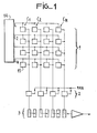
- FIG. 1 therefore represents the general organization of a line transfer structure, as described in the aforementioned French patent application.
- This structure mainly comprises a photosensitive zone 1, a line memory 2 and an analog shift register 3 for output.
- the photosensitive zone 1 receives the light image to be analyzed and transforms it into electrical charges. It should be noted that the aim here is by light image, the detection not only of the visible wavelengths but also of those which surround them, in particular in the infrared.
- the photosensitive zone is constituted by a plurality of elementary zones 15, also called below dots, arranged in N lines, identified L 1 , L 2 ... L N , and M columns, identified C 1 , C 2 ' .. C ,, and forming a matrix.
- the photosensitive points of the same line are linked together and connected to a control device 14, making it possible to address the lines one after the other; this device is constituted for example by a shift register of the MOS type.
- the photosensitive dots 15 of the same column are connected to the same connection, hereinafter called connection column, to line memory 2.
- the line memory 2 therefore receives in parallel the charges created in each of the photosensitive points 15 of the same line, then it also transfers them in parallel to the register 3, which is an analog shift register, of the CCD type, and which therefore provides the information, received in parallel, in serial mode; this information constitutes the video signal for analyzing the optical image received on the photosensitive zone 1.
- the content of the line memory 2 is transferred to the shift register 3, the input of the line memory being then closed.
- the next step corresponds to the line feed time during which the content of the line memory 2 is poured into the register 3, the latter having been completely read during the previous step.
- the selection of a line, its transfer to the line memory and then to the shift register are performed entirely during the return time.
- line time line being reserved for the updating of the reading means, which is all the better the longer it is, and for the serial evacuation of the shift register.
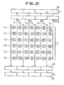
- FIG. 2 represents a first embodiment of the device according to the invention.
- the photosensitive matrix 1 has been diagrammed by its elementary zones, or points, 15, arranged in rows L (for example six rows L to L6 in the figure) and in columns C (for example seven columns C 1 to C 7 ).
- Each of the photosensitive dots is, as is known for taking a color photograph, covered with a colored filter so that it allows only one of three colors to pass, for example green, red or blue; in the figure, the photosensitive points 15 are marked R, G or B depending on whether they detect red, green or blue.
- the filters are distributed according to an inter-row staggered arrangement in which the points V, sensitive to green, more simply called “green points", are the most numerous because, as is known, it is those which give a maximum of sensitivity and therefore which are mainly used to obtain a luminance signal; moreover, the staggered arrangement makes it possible, as is also known, to increase the apparent resolution.
- This arrangement therefore consists of having a green point every two photosensitive points of each line, and of arranging these green points staggered from one line to another; on each line, the remaining photosensitive dots are alternately green or blue: we thus obtain the repetition of the green-red-green-blue sequence.
- the line memory 2 of FIG. 1 is here broken down into two memories, respectively 27 and 29, located on either side of the photosensitive matrix 1.
- One of these line memories (27) is connected to the connections of column of odd rank (noted c l , c 3 , c 5 and c 7 in the figure) while the other row memory (29) is connected to the column connections of even rank (c 2 , c 4 , c 6 and c 8 ).
- All the photosensitive points of the odd lines (L 1 , L 3 , L 5 ) are connected to a column connection which is on their left, all photosensitive dots of an even line (L 2 , L 4 ' L 6 ) are connected to the column connection which is on their right, with a line L starting with a green point, the column c 1 being located to its left . It can thus be seen that all the green dots are connected to the column connections of odd rank and therefore to the same row memory (27), the other photosensitive points being arranged so that the even column connections provide the color red. (columns c 2 and c 6 ) and the others, the blue color (c 4 and cg).
- each of the line memories 27 and 29 is connected in parallel an output register, respectively 37 and 39, analogous to the register 3 of FIG. 1.
- the register 37 which is connected to the memory 27 provides an electrical signal representing the only green color, which makes it possible to deduce therefrom the luminance signal; register 39 alternately supplies the blue chrominance signal and then the red chrominance signal, which can thus be easily separated downstream from the analysis device.
- This structure by reading the charges in two different directions, therefore makes it possible to facilitate the development of the luminance signal and the separation of the chrominance components.
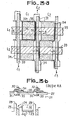
- FIG. 3a represents an embodiment of a matrix of photosensitive points capable of being used in the device of FIG. 2.
- a semiconductor substrate (not shown), in silicon for example, covered with an insulating layer, in silicon oxide for example, several conductive deposits 33, called below as the different deposits conductors of the device, electrodes or grids, possibly semi-transparent metallic or of polycrystalline silicon, parallel, representing the lines L of the matrix 1 of FIG. 2 (the lines L, and L 2 of the preceding figure, for example) and constituting with the semiconductor substrate and the insulator, photodetector MOS capacities.
- columns C of. the matrix (by example C ,, C 2 and C3) are placed grids 34, brought to a constant potential, which constitute a screen for the charges, according to a process described in more detail below.
- the device also includes, under each of the screen gates 34, a strip 35 produced in the semiconductor substrate, by doping for example, constituting a diode making it possible to read the different photosensitive points connected to the column considered.
- isolation barriers 31 in the form of vertical slots, shown in the figure in double lines, the horizontal parts of which are substantially in the middle of the space separating two grids 33, and the vertical parts are alternately left or right of the screen grids 34, without crossing them.
- Each of the isolation barriers 31 can be produced by a local excess thickness of the insulator, possibly accompanied by an overdoping of the semiconductor substrate, of the same type of conductivity as the latter (for example P overdoping for a P substrate), the overdoping intervening under the oxide excess thickness.
- a photosensitive point has been shown in thick lines, identified 30: it is bounded horizontally by the isolation barrier 31, on one of its vertical sides (right side in the example of the figure) by the same isolation barrier, and on its other. vertical side by the screen grid 34. According to a process described below, point 30 is read by the column diode 35 located to its left as indicated by an arrow 36 in the figure.
- each of the screen grids 34 is not in the form of a rectangular strip, but slightly in the form of vertical slots, like the isolation barriers 31 but of much smaller amplitude, in order to allow a maximum photosensitive surface: in fact, there is a minimum width for the screen grid between the photosensitive dot and the reading diode 35, but this width is of course not required. only on the side where this point is read: for example on the left side (arrow 36) for point 30 in the figure.
- the photosensitive point 30 is therefore formed of an MOS capacitance (semiconductor substrate, insulator and grid 33) constituting a first charge collection zone, and a second charge collection zone marked 38, consisting of two parts located between the grid 33 and the isolation barriers 30.
- MOS capacitance semiconductor substrate, insulator and grid 33
- the MOS capacity has a large charge storage capacity and thus makes it possible to obtain good dynamics for each photosensitive point, but grid 33 has greater absorption for the weak wavelengths, which are overcome by the second charge collection zone.
- a photodiode is formed in this zone 38, for example by doping the substrate, making it possible to increase the sensitivity of the point.
- This photodiode can be produced only in the space 38 between the grid 33 and the isolation barriers 30; it can also extend under the gate 33 in order to improve the electrical coupling between MOS capacitance and photodiode.
- These different embodiments of the second charge collection zone are also applicable to the different embodiments of the photosensitive matrix, described below.
- FIG. 3b represents a sectional view of FIG. 3a produced along a line AA, intersecting the photosensitive point 30 at the level of the MOS capacity grid 33.
- the structure of the device of FIG. 3a appears more clearly: it is produced in a semiconductor substrate 21, covered with an insulating layer 22, two isolation barriers 31 by excess thickness of insulator and a reading diode 35 to the right of each of the barriers 31, by doping the substrate.
- On the insulating layer 22 are deposited the screen grids 34 at the edge and to the right of the isolation barriers 31.
- the grid of the MOS capacity 33 extends over the substrate and above the screen grids 34, via 'a layer of insulation, not shown for clarity of the drawing.
- the device further comprises a metallization 32 deposited on the grid 33, by means of an insulating layer, at right of each of the diodes 35 and shown only in Figure 3b.
- These metal strips 32 have the function of constituting a screen opaque to light radiation which would be liable to create parasitic charges in the reading diodes 35. They can be made, for example, of aluminum.
- FIG. 4 represents another embodiment of the device according to the invention, suitable for the case where the reading of the photosensitive zone is done by interlaced half-frames, that is to say starting with the half-frame constituted by the odd order lines (odd half frame) then following by the half frame constituted by the even order lines (even half frame).
- each of the lines of a device such as that of FIG. 2 should be split to obtain an identical signal for each half-frame, which is necessary for good image quality on rendering .
- FIG. 4 there is a matrix 1 of six rows (L) and six columns (C) of photosensitive dots 15 to each of which is assigned a color (R, G or B), the green photosensitive dots being distributed in the same way as before.
- the remaining points are distributed so that a line is only two-color (green..and blue or green and red), the color information varying only once every two lines: for example line L 1 comprises alternately a green point and a blue point, and no red point; line L 2 alternately comprises red and green points, and no blue point; the same for line L 3 ; the lines L 4 and L 5 are again alternately blue and green, the line L 6 being alternately red and green, the point of the line L 1 and of the column CI being for example a blue point.
- the signal collected on each of the columns can be directed either to the line memory 27 or to the line memory 29.
- the devices 47 and 49 appropriately, described in more detail below, it is obtained in line memory 27 and therefore at the output of the associated shift register 37, only a signal representing the green chrominance information from which the luminance information is deduced, and on the line memory 29 and therefore at the output of the shift register 39 , successively a blue line then a red line in the same half-frame. The color separation is then complete and the alternation of red and then blue lines is adapted to the SECAM process.
- Figure 4a an alternative embodiment which consists of grouping the column connections in pairs between the columns of photosensitive dots, which increases the photosensitive area compared to that which is reserved for reading.
- the switching device 47 is constituted by six switching devices, for example MOS transistors, placed respectively on the six columns (C 1 to C6), those which are placed on the odd columns, marked 41 , being controlled by a potential 0 p applied to their grid, and those placed on the even columns, marked 42, are controlled by a potential ⁇ I also applied to their grid.
- the switching device 49 is made up of six MOS transistors interposed on the six columns C to C 6 respectively, the transistors of the odd columns (43) being controlled by the signal ⁇ I and the transistors of the even columns ( 44), by the signal ⁇ p. These transistors are polarized in triode when they are opened by the signals ⁇ 1 and ⁇ P.
- the potential ⁇ y is represented as a function of time; it is a function in time slots of period T, varying between a lower value noted V B and a higher value noted V H , the duration (between instants t 2 to t 3 in the figure) of the upper time slot (V H ) being slightly lower than T / 2.
- the poten tiel ⁇ P is analogously a square wave signal varying between a lower value V B and a higher value V H , which are for example equal to those of the signal ⁇ I , the period of ⁇ P being equal to the period T and the duration (of instants t 5 to t 6 ) of the upper slot (V H ), less than T / 2.
- the signal ⁇ P is in phase opposition with the signal ⁇ I , that is to say that the low square wave (V B ) begins at an instant t a prior to the instant t 2 , and that the upper square wave ( V H ) begins at time t 5 after time t 3 .
- the duration of the reading of a frame is equal to T; the odd frame is read (lines L 1 , L 3 and L 5 ) is carried out between times t 1 and t 4 , t 1 being between t 0 and t 2 and t 4 between t 3 and t 5 , the reading of the even half-frame (lines L 2 , L 4 and L 6 ) operating between the instants t 4 and t 7 , t 7 being analogous to the instant t l ; the duration of the odd frame is marked I on the diagram, and the duration of the even half-frame, by P.
- the signal ⁇ I is at the high level (VH), which results in the orientation of the charges stored in the blue and red points of the odd columns towards the line memory 29 thanks to the transistors 43 which, controlled by ⁇ I , are then conductive, the transistors 41, controlled by ⁇ P then at the low level, preventing access to memory 27.
- the even columns which include points sensitive to green on the odd lines are read in the direction of the line memory 27 only thanks to the transistors 42 which are then conductive, while the transistors 44 are not.
- the odd columns which have green dots on the even lines are read in the direction of the line memory 27 thanks to the transistors 41 which are then conductive, the signal ⁇ P being at the high level, while the signal ⁇ is at the low level, preventing access to the line memory 29 (non-conductive transistors 43).
- the reading of the even columns which carry on the odd lines alternately red and blue points are read in the direction of the memory of line 29 thanks to the 44 conductive transistors, the non-conductive transistors 42 preventing access to the line memory 27.
- each line of the structure of FIG. 4a one of the lines of the same pair belonging to the odd half-frame and the other, to the half- even frame.
- all the green dots for example are, from one line to another, sometimes connected to the even column connections, sometimes to the odd.
- the period (T) of the signals 0, and 0 p must no longer be the frame period, but the period line.
- the advantage of this variant is that then, the colored structure of two half-frames is perfectly identical.
- the vertical resolution may be twice lower for the color filters, which can then extend over two lines at the same time.
- the distribution of the colored filters differs from FIG. 4a in the sense that the green filters are now aligned.
- the photosensitive dots of the same column are always connected to the same column connection and the reading is done by interlaced half-frames. There is no longer any need for switching devices to obtain alternating blue and red lines on one of the green outputs and on the other output.
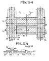
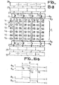
- FIG. 5a represents a top view and FIG. 5b a sectional view of an embodiment of a photosensitive dot matrix in which the grouping of the column connections illustrated in Figure 4a.
- FIG. 5a the grids 33, separated from each other by isolation barriers 51 produced as above. Between the grids 33 and the isolation barriers 51 are located the zones 38 in which are produced, in the variant shown, photodiodes.
- One of photosensitive points thus constituted is surrounded by a thick line and spotted 50 Figure 5a: it belongs to the L line. and in column Ci and the charges it stores are read to the left as represented by an arrow 56.
- the reading columns are grouped by two on either side of a vertical isolation barrier, also marked 51. There are therefore on each side of the isolation 51, two column diodes marked 35 and produced as above, for example in the substrate 21 (FIG. 5b).
- the screen grid is now marked 54 and covers both the isolation barrier 51 and the two reading diodes 35 which are located on either side of the barrier 51.
- the MOS capacitance grid 33 covers the substrate 21 and the screen grids 54, by means of an insulating layer.
- an opaque layer 32 is placed above the reading diodes 35; in the present case, a single layer 32 is deposited for the two reading diodes located on either side of the same barrier 51.
- FIG. 5b shows the case where photodiodes are produced in the zones 38 which also extend under the grid of MOS capacities 33, outside the zones occupied by the screen grids-54 and the isolation barriers 51.
- FIG. 6a represents a variant of the embodiment of FIG. 4a in which the double column is replaced by a single column, the isolation between the photosensitive points being carried out by independent screen grids.
- the photosensitive matrix 1 which comprises for example six rows (L 1 to L 6 ) and eight columns (C 1 to C 8 ), the colored filters being distributed in the same way as in FIG. 4a , and the two line memories 27 and 29 located on either side of the matrix 1, connected respectively to the two shift registers 37 and 39.
- the device here comprises two switching elements 67 and 69 interposed respectively before the line memories 27 and 29.
- the columns C 1 to C 8 that constitute the photosensitive dots are connected two by two to the same column connection (c 1 to c 4 in the figure), which comprises a reading diode 35, illustrated in FIG. 6a by a simple connection, surrounded by two screen grids on either side of the reading diode 35, these grids being marked 64 for the column C 1 and 74 for column C 2 .
- the screen grids such as 64 which correspond to the odd columns (C l , C 3 , C 5 ' C 7 ), are connected to a potential ⁇ G
- the screen grids such as 74 connected to the even columns (C 2 , C 4 , C 6 and C 8 ) are connected to a potential ⁇ D.
- the reading diodes 35 are connected, at each of their ends, to the memories 27 and 29 respectively by means of transistors 61 and 62, controlled respectively by potentials ⁇ B and ⁇ H , these transistors respectively constituting the switching devices 67 and 69.
- FIG. 6b represents the form of the control signals 0 B, ⁇ H , ⁇ G and ⁇ D used in the device of FIG. 6a, which are voltages varying between a high level and a low level.
- the signal ⁇ B is only high between time t 8 and time t 9 , t 9 -t 8 being slightly less than D / 2;
- the signal ⁇ H is in the high state only between an instant t 10 and the instant t 11 , with t 11 - t 10 slightly less than D / 2;
- the signals ⁇ G and ⁇ D respectively have the same form as the signals ⁇ B and ⁇ H.
- the operation of the device is as follows.
- the signals ⁇ B and ⁇ G returned to the low level while the signals ⁇ H and ⁇ D are at the high level and the operation is then inverse of the previous one, that is to say that this are the charges stored in the photosensitive points of the even columns which are discharged by the diode 35 and they are directed towards the line memory 29 exclusively via the transistors 62, the only conductors.
- Figure 7a shows a top view and Figure 7b a sectional view of an embodiment of a photosensitive matrix capable of being used in the device of Figure 6a.
- This structure differs from that of FIG. 5a only at the level of the charge collecting columns.
- the photosensitive point 50 constituted by an MOS capacitance produced by the grid 33, the semiconductor substrate 21 and the insulator 22, and a zone 38 in which a photodiode has been produced which extends for example also under the grid 33 , limited by the elements 51 and 74, as shown in the section of FIG. 7b, produced in the device of FIG. 7a along a line CC, at the photosensitive point 50 and the grid 33.
- the reading of this point is made from the left (arrow 56).
- the charge collection column is here constituted by a column diode 35 partially covered by the screen grid 64, the latter also extending above the substrate 21 to the left of the reading diode 35.
- the grid. screen 74 covers the other part of the diode 35, extends over a part of the substrate situated to the right of this diode and also extends, by means of an insulating layer, above the grid screen 64.
- the assembly is covered with the grid 33, above which the opaque layer 32 is still arranged by means of an insulating layer, at the level of the diode 35.
- the advantage of the structure as described in FIGS. 6 and 7 is the elimination of the insulation between two columns and, consequently, an increase in sensitivity. For example, this increase can reach 30% compared to a structure such as that of FIG. 3.
- the invention is not limited to the embodiments described above but encompasses all the variants which are within the reach of those skilled in the art. This is how the arrangement of the colored filters has been described with the three classic colors green, blue and red, but can of course be applied to the three complementary colors. previous ones, or to other sets of three colors, such as green, yellow and white or green, yellow and cyan for example.
Abstract
Le dispositif d'analyse électrique d'images lumineuses en couleur selon l'invention comporte principalement: - une matrice (1) de points photosensibles (15) susceptibles de recevoir chacun un filtre coloré (V, R, B); - un ensemble de deux mémoires de ligne (27, 29) recevant en parallèle les charges électriques d'une ligne de la matrice (1); - deux registres à décalage (37, 39) recevant en parallèle respectivement les charges fournies par les deux mémoires de ligne (27, 29). Ce dispositif est notamment applicable à une caméra de télévision.The device for the electrical analysis of bright color images according to the invention mainly comprises: - a matrix (1) of photosensitive dots (15) each capable of receiving a color filter (V, R, B); - a set of two line memories (27, 29) receiving in parallel the electric charges of a line of the matrix (1); - two shift registers (37, 39) receiving in parallel respectively the charges provided by the two line memories (27, 29). This device is particularly applicable to a television camera.
Description
La présente invention se rapporte au domaine de l'analyse électrique d'images lumineuses utilisant le transfert de charges dans un semiconducteur ; elle a pour objet un dispositif plus particulièrement adapté à l'analyse d'images en couleur.The present invention relates to the field of electrical analysis of light images using charge transfer in a semiconductor; it relates to a device more particularly suited to the analysis of color images.
On connaît différents dispositifs à l'état solide pour l'analyse d'une image lumineuse, qui sont destinés à être utilisés dans une caméra de télévision pour fournir un signal électrique vidéo. Ils se distinguent par le mode de réalisation de la zone photosensible d'une part, et le système de lecture et d'évacuation des charges créées par l'image, d'autre part.Various solid state devices are known for analyzing a light image, which are intended to be used in a television camera to provide an electrical video signal. They are distinguished by the embodiment of the photosensitive area on the one hand, and the system for reading and discharging the charges created by the image, on the other hand.
Il est également connu d'utiliser des dispositifs à transfert de charges pour réaliser ces différentes fonctions, comme il est décrit par exemple dans l'ouvrage de SEQUIN et TOMPSETT, intitulé "Charge transfer devices", (pages 152 à 169) :
- - dans des organisations dites "à transfert de trame" ou "à structure interligne", dans lesquelles le rayonnement lumineux est reçu sur des registres à transfert de charges ; dans ces dispositifs, le transfert de charges est réalisé sur de grandes surfaces, ce qui constitue un inconvénient du fait qu'il est actuellement difficile d'obtenir des rendements élevés pour la fabrication de ces grandes surfaces;
- dans des dispositifs dits "CID" (pour "Charge Injection Devices") qui ne présentent pas cet inconvénient mais qui nécessitent en général une réinjection des charges dans le substrat semiconducteur, ce qui présente un certain nombre d'inconvénients parmi lesquels du bruit ou des difficultés au niveau des valeurs des capacités nécessaires pendant ou après la lecture des charges.
- - in so-called "frame transfer" or "interline structure" organizations, in which the light radiation is received on charge transfer registers; in these devices, the transfer of charges is carried out over large areas, which constitutes a drawback because it is currently difficult to obtain high yields for the manufacture of these large areas;
- in so-called "CID" devices (for "Charge Injection Devices") which do not have this drawback but which generally require reinjection of the charges into the semiconductor substrate, which has a certain number of drawbacks, including noise or difficulties with the values of the capacities required during or after reading the loads.
Plus généralement, en sus des problèmes évoqués ci-dessus, se pose la question de la compatibilité des temps nécessaires d'une part à l'intégration lumineuse et d'autre part au transfert des charges dans le cas où cette solution est retenue, avec les temps de balayage de l'écran de télévision qui sont, selon le standard 625 lignes habituel, environ de 52 µs pour le temps d'affichage d'une ligne et de 12 µs pour le temps de retour ligne.More generally, in addition to the problems mentioned above, there is the question of the compatibility of the times required on the one hand with the light integration and on the other hand with the transfer of the charges in the case where this solution is selected, with the times of scanning of the television screen which are, according to the standard 625 lines, approximately of 52 µs for the display time of a line and 12 µs for line feed time.
Pour répondre à ces différents impératifs, la Demanderesse a proposé une structure dite "à transfert de ligne", décrite dans la demande de brevet français n° 80-08112, qui comporte principalement :
- - une matrice de N lignes x M zones, ou points photosensibles, matrice sur laquelle une image à lire est projetée et convertie en charges électriques ;
- - une mémoire de M points, dite mémoire de ligne, destinée à recevoir successivement les charges signal stockées par chaque ligne ;
- - un registre à décalage du type CCD (pour "Charge Coupled Devices"), recevant en parallèle le contenu de la mémoire de ligne et délivrant en série le signal électrique d'analyse de l'image.
- - a matrix of N lines x M zones, or photosensitive points, matrix on which an image to be read is projected and converted into electrical charges;
- - a memory of M points, called line memory, intended to successively receive the signal charges stored by each line;
- - a shift register of the CCD type (for "Charge Coupled Devices"), receiving in parallel the content of the line memory and delivering in series the electrical image analysis signal.
La présente invention a pour objet des perfectionnements à la structure du dispositif à transfert de ligne décrit ci-dessus, visant à l'adapter à l'analyse d'images en couleur.The present invention relates to improvements to the structure of the line transfer device described above, aimed at adapting it to the analysis of color images.
A cet effet, le dispositif d'analyse d'images selon l'invention comporte :
- - un ensemble photosensible, comportant :
- - une pluralité de zones photosensibles élémentaires, appelées points, dans lesquelles sont créées des charges électriques en fonction de l'éclairement reçu, réalisées sur un même substrat semiconducteur selon N lignes et M colonnes et isolées les unes des autres, formant une matrice, chacune de ces zones élémentaires comportant une capacité MOS, constituant une première zone de collection de charges et comportant une ,grille qui est commune aux capacités d'une même ligne, et une seconde zone de collection de charges, électriquement couplée à la capacité, l'ensemble du point recevant un filtre coloré destiné à ne le rendre sensible qu'à une couleur prédéfinie ;
- - des moyens de connexion et de commande, assurant la fourniture en parallèle, par l'intermédiaire de connexions de colonne, des charges électriques créées dans les M points d'une même ligne, successivement pour les N lignes, ces moyens comportant une pluralité de diodes de lecture, arrangées en colonnes entre les points de façon à recevoir chacune, successivement, sur commande, les charges d'au moins deux points appartenant à deux lignes différentes ;
- - des moyens formant écran pour les charges, placés entre chacun des points et les moyens de connexion, ces moyens écran comportant une pluralité de grilles, portées à un potentiel constant, arrangées en colonnes entre les diodes de lecture et les points ;
- - un ensemble de deux mémoires de M points chacune, dites mémoires de ligne, réalisées dans le même substrat semiconducteur, recevant en parallèle les charges électriques fournies par les moyens de connexion et de commande de telle sorte que chaque point de la matrice soit affecté à l'une seulement des deux mémoires de ligne, l'une de ces mémoires n'étant reliée qu'aux points d'une même couleur ;
- - un ensemble de deux registres à décalage analogiques, recevant en parallèle respectivement les charges fournies par les deux mémoires de ligne et délivrant en série chacun un signal électrique d'analyse de l'image.
- - a photosensitive assembly, comprising:
- a plurality of elementary photosensitive zones, called points, in which electrical charges are created as a function of the illumination received, produced on the same semiconductor substrate according to N rows and M columns and isolated from each other, forming a matrix, each of these elementary zones comprising a MOS capacity, constituting a first charge collection zone and comprising a grid which is common to the capacities of the same line, and a second charge collection zone, electrically coupled to the capacity, the set of point receiving a color filter intended to make it sensitive only to a predefined color;
- - connection and control means, ensuring the parallel supply, via column connections, of the electric charges created in the M points of the same line, successively for the N lines, these means comprising a plurality of reading diodes, arranged in columns between the points so as to each receive, successively, on command, the charges of at least two points belonging to two different lines;
- - screen means for the charges, placed between each of the points and the connection means, these screen means comprising a plurality of grids, brought to a constant potential, arranged in columns between the reading diodes and the points;
- - a set of two memories of M points each, called line memories, produced in the same semiconductor substrate, receiving in parallel the electric charges provided by the connection and control means so that each point of the matrix is assigned to only one of the two line memories, one of these memories being connected only to points of the same color;
- - a set of two analog shift registers, receiving in parallel respectively the charges provided by the two line memories and each delivering in series an electrical image analysis signal.
L'invention a également pour objet une caméra de télévision comportant un tel dispositif d'analyse d'images.The invention also relates to a television camera comprising such an image analysis device.
L'invention est décrite, à titre d'exemple non limitatif, plus en détail dans ce qui suit à l'aide des figures annexées, qui représentent :
- - la figure 1, l'organisation générale d'une structure à transfert de ligne ; ;
- - la figure 2, un premier mode de réalisation du dispositif selon l'invention ;
- - la figure 3a, une vue de dessus et la figure 3b, une vue en coupe d'une matrice de points photosensibles susceptible d'être utilisée dans le dispositif de la figure 2 ;
- - la figure 4a, un deuxième mode de réalisation du dispositif selon l'invention, et la figure 4b, des diagrammes de signaux relatifs à la figure 4a ;
- - la figure 5a, une vue de dessus et la figure 5b, une vue en coupe d'un mode de réalisation d'une matrice de points photosensibles utilisable dans le dispositif de la figure 4a ;
- - la figure 6a, une variante de réalisation de la figure 4, et la figure 6b, des diagrammes de signaux relatifs à la figure 6a ;
- - la figure 7a, une vue de dessus et la figure 7b, une vue en coupe d'un mode de réalisation d'une matrice de points photosensibles susceptible d'être utilisée dans le dispositif de la figure 6a.
- - Figure 1, the general organization of a line transfer structure; ;
- - Figure 2, a first embodiment of the device according to the invention;
- - Figure 3a, a top view and Figure 3b, a view section of a matrix of photosensitive points capable of being used in the device of FIG. 2;
- - Figure 4a, a second embodiment of the device according to the invention, and Figure 4b, signal diagrams relating to Figure 4a;
- - Figure 5a, a top view and Figure 5b, a sectional view of an embodiment of a matrix of photosensitive dots usable in the device of Figure 4a;
- - Figure 6a, an alternative embodiment of Figure 4, and Figure 6b, signal diagrams relating to Figure 6a;
- - Figure 7a, a top view and Figure 7b, a sectional view of an embodiment of a matrix of photosensitive dots that can be used in the device of Figure 6a.
Sur ces différentes figures, les mêmes références se rapportent aux mêmes éléments.In these different figures, the same references relate to the same elements.
La figure 1 représente donc l'organisation générale d'une structure à transfert de lignes, telle que décrite dans la demande de brevet français précitée.FIG. 1 therefore represents the general organization of a line transfer structure, as described in the aforementioned French patent application.
Cette structure comporte principalement une zone photosensible 1, une mémoire de ligne 2 et un registre à décalage 3 analogique de sortie.This structure mainly comprises a
La zone photosensible 1 reçoit l'image lumineuse à analyser et la transforme en charges électriques. Il est à noter qu'on vise ici par image lumineuse, la détection non seulement des longueurs d'onde visibles mais également de celles qui les entourent, notamment dans l'infrarouge. La zone photosensible est constituée par une pluralité de zones élémentaires 15, également appelées ci-dessous points, arrangées en N lignes, repérées L1, L2...LN, et M colonnes, repérées C1, C2'..C,, et formant une matrice. Les points photosensibles d'une même ligne sont reliés entre eux et reliés à un dispositif de commande 14, permettant d'adresser les lignes les unes après les autres ; ce dispositif est constitué par exemple par un registre à décalage du type MOS. Les points photosensibles 15 d'une même colonne sont reliés à une même connexion, dite ci-après connexion de colonne, vers la mémoire de ligne 2.The
La mémoire de ligne 2 reçoit donc en parallèle les charges créées dans chacun des points photosensibles 15 d'une même ligne, puis elle les transfère également en parallèle vers le registre 3, qui est un registre à décalage analogique, du type CCD, et qui fournit donc l'information, reçue en parallèle, en mode série ; cette information constitue le signal vidéo d'analyse de l'image optique reçue sur la zone photosensible 1.The
L'enchaînement des différentes opérations d'intégration de l'image au niveau de la zone photosensible 1, du transfert des lignes dans la mémoire de ligne 2, puis du transfert des signaux dans le registre 3, pour les différentes lignes, est maintenant décrit.The sequence of the various operations of integration of the image at the level of the
Tout d'abord, il est à noter que l'intégration de l'image est réalisée en permanence sur la totalité de la matrice photosensible 1, sauf sur celle des lignes qui est adressée par le registre 14.First of all, it should be noted that the integration of the image is carried out permanently on the whole of the
Pendant le temps de retour ligne, le contenu de la mémoire de ligne 2 est transféré dans le registre à décalage 3, l'entrée de la métnoire de ligne étant alors fermée.During the line return time, the content of the
Pendant le temps ligne qui suit, le contenu du registre 3 est évacué en série, la connexion entre la mémoire de ligne 2 et le registre 3 est interrompue. Pendant ce temps, il se produit, dans une première phase, une remise à niveau des moyens de lecture des points 15, par l'intermédiaire de la connexion repérée RAN sur la figure 1, reliée à la mémoire de ligne 2 et, dans une deuxième phase, on opère le transfert de l'une des lignes L de la zone 1 vers la mémoire de ligne 2, la sélection (ou "adressage") d'une ligne étant assurée par le registre 14.During the following line time, the content of
L'étape suivante correspond au temps de retour ligne pendant .lequel s'opère le déversement du contenu de la mémoire de ligne 2 dans le registre 3, celui-ci ayant été entièrement lu lors de l'étape précédente.The next step corresponds to the line feed time during which the content of the
Dans un autre mode de réalisation, la sélection d'une ligne, son transfert dans la mémoire de ligne puis dans le registre à décalage s'effectuent entièrement pendant le temps de retour. ligne, le temps de ligne étant réservé à la remise à niveau des moyens de lecture, qui est d'autant meilleure qu'elle est plus longue, et à l'évacuation en série du registre à décalage.In another embodiment, the selection of a line, its transfer to the line memory and then to the shift register are performed entirely during the return time. line time line being reserved for the updating of the reading means, which is all the better the longer it is, and for the serial evacuation of the shift register.
La figure 2 représente un premier mode de réalisation du dispositif selon l'invention.FIG. 2 represents a first embodiment of the device according to the invention.
Sur cette figure, on a schématisé la matrice photosensible 1 par ses zones élémentaires, ou points, 15, arrangées en lignes L (par exemple six lignes L à L6 sur la figure) et en colonnes C (par exemple sept colonnes C1 à C7). Chacun des points photosensibles est, ainsi qu'il est connu pour réaliser une prise de vue en couleur, recouvert d'un filtre coloré de telle sorte qu'il ne laisse passer que l'une parmi trois couleurs, par exemple vert, rouge ou bleu ; sur la figure, les points photosensibles 15 sont repérés R, V ou B selon qu'ils détectent le rouge, le vert ou le bleu. Les filtres sont répartis selon un arrangement en quinconce interligne dans lequel les points V, sensibles au vert, appelés plus simplement "points verts", sont les plus nombreux du fait que, ainsi qu'il est connu, ce sont ceux qui donnent un maximum de sensibilité et donc qui sont principalement utilisés pour obtenir un signal de luminance ; de plus, le quinconce permet, ainsi qu'il est également connu, d'augmenter la résolution apparente. Cet arrangement consiste donc à avoir un point vert tous les deux points photosensibles de chaque ligne, et de disposer ces points verts en quinconce d'une ligne à l'autre ; sur chaque ligne, les points photosensibles restants sont alternativement verts ou bleus : on obtient ainsi la répétition de la séquence vert- rouge-vert-bleu.In this figure, the
La mémoire de ligne 2 de la figure 1 est ici décomposée en deux mémoires, respectivement 27 et 29, situées de part et d'autre de la matrice photosensible 1. L'une de ces mémoires de ligne (27) est reliée aux connexions de colonne de rang impair (notées cl, c3, c5 et c7 sur la figure) alors que l'autre mémoire de ligne (29) est reliée aux connexions de colonne de rang pair (c2, c4, c6 et c8). Tous les points photosensibles des lignes impaires (L1, L3, L5) sont reliés à une connexion de colonne qui se trouve à leur gauche, tous les points photosensibles d'une ligne paire (L2, L4' L6) sont reliés à la connexion de colonne qui se trouve à leur droite, avec une ligne L commençant par un point vert, la colonne c1 étant située à sa gauche. On constate ainsi que tous les points verts sont reliés aux connexions de colonne de rang impair et donc à une même mémoire de ligne (27), les autres points photosensibles étant disposés de telle sorte que les connexions de colonne paires fournissent les unes la couleur rouge (colonnes c2 et c6) et les autres, la couleur bleue (c4 et cg).The
A chacune des mémoires de ligne 27 et 29 est relié en parallèle un registre de sortie, respectivement 37 et 39, analogues au registre 3 de la figure 1. De la sorte, le registre 37 qui est relié à la mémoire 27 fournit un signal électrique représentant la seule couleur verte, ce qui permet d'en déduire le signal de luminance ; le registre 39 fournit alternativement le signal de chrominance bleu puis le signal de chrominance rouge, qui peuvent être ainsi aisément séparés en aval du dispositif d'analyse.To each of the
Cette structure, en réalisant la lecture des charges dans deux directions différentes, permet donc de faciliter l'élaboration du signal de luminance et la séparation des composantes de la chrominance.This structure, by reading the charges in two different directions, therefore makes it possible to facilitate the development of the luminance signal and the separation of the chrominance components.
La figure 3a représente un mode de réalisation d'une matrice de points photosensibles susceptible d'être utilisée dans le dispositif de la figure 2.FIG. 3a represents an embodiment of a matrix of photosensitive points capable of being used in the device of FIG. 2.
Sur cette figure, on a représenté, déposés sur un substrat semiconducteur (non représenté), en silicium par exemple, recouvert d'une couche isolante, en oxyde de silicium par exemple, plusieurs dépôts conducteurs 33, appelés ci-dessous comme les différents dépôts conducteurs du dispositif, électrodes ou grilles, métalliques éventuellement semi-transparents ou en silicium polycristallin, parallèles, représentant les lignes L de la matrice 1 de la figure 2 (les lignes L, et L2 de la figure précédente, par exemple) et constituant avec le substrat semiconducteur et l'isolant, des capacités MOS photodétectrices. Selon les colonnes C de. la matrice (par exemple C,, C2 et C3) sont placées des grilles 34, portées à un potentiel constant, qui constituent un écran pour les charges, selon un processus décrit plus en détail ci-dessous. Le dispositif comporte encore sous chacune des grilles écran 34 une bande 35 réalisée dans le substrat semiconducteur, par dopage par exemple, constituant une diode permettant de réaliser la lecture des différents points photosensibles reliés à la colonne considérée.In this figure, there is shown, deposited on a semiconductor substrate (not shown), in silicon for example, covered with an insulating layer, in silicon oxide for example, several
Les différentes lignes L et les différentes colonnes C sont séparées les unes des autres par des barrières d'isolement 31 en forme de créneaux verticaux, représentées sur la figure en doubles traits, dont les parties horizontales sont sensiblement au milieu de l'espace séparant deux grilles 33, et les parties verticales sont alternativement à gauche ou à droite des grilles écran 34, sans les traverser. Chacune des barrières d'isolement 31 peut être réalisée par une surépaisseur locale de l'isolant, éventuellement accompagnée par un surdopage du substrat semiconducteur, du même type de conductivité que celùi-ci (par exemple surdopage P pour un substrat P), le surdopage intervenant sous la surépaisseur d'oxyde.The different lines L and the different columns C are separated from each other by isolation barriers 31 in the form of vertical slots, shown in the figure in double lines, the horizontal parts of which are substantially in the middle of the space separating two
On a représenté à titre d'exemple en traits épais un point photosensible, repéré 30 : il est limité horizontalement par la barrière d'isolement 31, sur l'un de ses côtés verticaux (côté droit dans l'exemple de la figure) par la même barrière d'isolement, et sur son autre. côté vertical par la grille écran 34. Selon un processus décrit ci-dessous, le point 30 est lu par la diode colonne 35 située à sa gauche comme l'indique une flèche 36 sur la figure. Dans la variante de réalisation représentée sur la figure, chacune des grilles écran 34 est non pas en forme de bande rectangulaire, mais légèrement en forme de créneaux verticaux, comme les barrières d'isolement 31 mais de beaucoup plus faible amplitude, afin de permettre un maximum de surface photosensible : en effet, il existe un minimum de largeur pour la grille écran entre le point photosensible et la diode de lecture 35, mais cette largeur n'est bien entendu requise . que du côté où ce point est lu : par exemple côté gauche (flèche 36) pour le point 30 de la figure.By way of example, a photosensitive point has been shown in thick lines, identified 30: it is bounded horizontally by the isolation barrier 31, on one of its vertical sides (right side in the example of the figure) by the same isolation barrier, and on its other. vertical side by the
Le point photosensible 30 est donc formé d'une capacité MOS (substrat semiconducteur, isolant et grille 33) constituant une première zone de collection de charges, et d'une seconde zone de collection de charges repérée 38, constituée de deux parties situées entre la grille 33 et les barrières d'isolement 30. En effet, la capacité MOS a une grande capacité de stockage de charges et permet ainsi d'obtenir une bonne dynamique pour chaque point photosensible, mais la grille 33 présente une absorption plus grande pour les faibles longueurs d'onde, dont on s'affranchit par la seconde zone de collection de charges. Dans une variante de réalisation, on forme dans cette zone 38 une photodiode, par exemple par dopage du substrat, permettant d'accroître la sensibilité du point. Cette photodiode peut être réalisée seulement dans l'espace 38 compris entre la grille 33 et les barrières d'isolement 30 ; elle peut également s'étendre sous la grille 33 afin d'améliorer le couplage électrique entre capacité MOS et photodiode. Ces différentes variantes de réalisation de la seconde zone de collection des charges sont également applicables aux différents modes de réalisation de la matrice photosensible, décrits plus loin.The photosensitive point 30 is therefore formed of an MOS capacitance (semiconductor substrate, insulator and grid 33) constituting a first charge collection zone, and a second charge collection zone marked 38, consisting of two parts located between the
La figure 3b représente une vue en coupe de la figure 3a réalisée selon une ligne AA, coupant le point photosensible 30 au niveau de la grille de capacité MOS 33.FIG. 3b represents a sectional view of FIG. 3a produced along a line AA, intersecting the photosensitive point 30 at the level of the
Sur cette figure, la structure du dispositif de la figure 3a apparaît plus clairement : il est réalisé dans un substrat semiconducteur 21, recouvert d'une couche isolante 22, deux barrières d'isolement 31 par surépaisseur d'isolant et une diode de lecture 35 à la droite de chacune des barrières 31, par dopage du substrat. Sur la couche isolante 22 sont déposées les grilles écran 34 en bordure et à droite des barrières d'isolement 31. La grille de la capacité MOS 33 s'étend sur le substrat et au-dessus des grilles écran 34, par l'intermédiaire d'une couche d'isolant, non représentée pour la clarté du dessin.In this figure, the structure of the device of FIG. 3a appears more clearly: it is produced in a
Le dispositif comporte en outre une métallisation 32 déposée sur la grille 33, par l'intermédiaire d'une couche d'isolant, au droit de chacune des diodes 35 et représentée uniquement sur la figure 3b. Ces bandes métalliques 32 ont pour fonction de constituer un écran opaque aux rayonnements lumineux qui seraient susceptibles de créer des charges parasites dans les diodes de lecture 35. Elles peuvent être réalisées par exemple en aluminium.The device further comprises a
Le fonctionnement du dispositif représenté sur la figure 3a sera plus clairement expliqué à l'aide du profil du potentiel de surface qui est représenté sous la coupe de la figure 3b.The operation of the device shown in Figure 3a will be more clearly explained using the profile of the surface potential which is shown in the section of Figure 3b.
Sur ce diagramme, les potentiels sont représentés croissants vers le bas du schéma, ce qui correspond au fait que, appliqués sur une électrode, ils créent un puits de potentiel permettant d'emprisonner les charges.On this diagram, the potentials are shown increasing towards the bottom of the diagram, which corresponds to the fact that, applied to an electrode, they create a potential well allowing the charges to be trapped.
Lorsqu'une ligne n'est pas adressée par le registre 14 (figure 1), son potentiel est à une valeur donnée représentée par la ligne 23 sur le schéma de la figure 3b, au droit de la grille de la capacité MOS 33, limitée de part et d'autre par des potentiels plus faibles : un potentiel représenté par une ligne 28, correspondant aux barrières d'isolement 31, et un potentiel constant VE appliqué à la grille écran 34, représenté par une ligne 24, dont la valeur est choisie plus faible que la valeur appliquée à la grille 33 de façon à former un puits de potentiels sous cette grille, dans lequel les charges créées par l'éclairement peuvent être stockées (zone hachurée repérée Q sur la figure). Au droit de la diode de lecture 35, le potentiel est, avant lecture du point photosensible considéré, ramené à une valeur donnée illustrée par le niveau 25, par les moyens de remise à niveau schématisés sur la figure 1, la valeur de ce potentiel devant être plus élevée que celle du potentiel VE afin qu'il n'y ait pas invasion par des charges parasites des puits de potentiels situés au droit des grilles 33.When a line is not addressed by the register 14 (FIG. 1), its potential is at a given value represented by the line 23 in the diagram of FIG. 3b, in line with the grid of the
Lorsque le point photosensible considéré est, en même temps que tous les points photosensibles de la ligne à laquelle il appartient, sélectionné par le registre 14, le potentiel qui est appliqué à la grille 33 est ramené à une valeur proche de zéro, ce qui est illustré par la ligne 26 sur la figure 3b : ce potentiel étant alors inférieur à VE (ligne 24), les charges accumulées lors de la phase précédente sont donc déversées dans la diode 35, comme indiqué par une flèche sur la figure 3b, pour être évacuées vers l'une des mémoires de ligne 27 ou 29 ; dans l'exemple de la figure, les charges sont évacuées par l'intermédiaire de la colonne c1 vers la mémoire de ligne 27.When the photosensitive point considered is, at the same time as all the photosensitive points of the line to which it belongs, selected by the register 14, the potential which is applied to the
La figure 4 représente un autre mode de réalisation du dispositif selon l'invention, adapté au cas où la lecture de la zone photosensible se fait par demi-trames entrelacées, c'est-à-dire en commençant par la demi-trame constituée par les lignes d'ordre impair (demi-trame impaire) puis en suivant par la demi-trame constituée par les lignes d'ordre pair (demi-trame paire). En effet, dans ce cas, chacune des lignes d'un dispositif tel que celui de la figure 2 devrait être dédoublée pour obtenir à chaque demi-trame un signal identique, ce qui est nécessaire pour une bonne qualité de l'image à la restitution.FIG. 4 represents another embodiment of the device according to the invention, suitable for the case where the reading of the photosensitive zone is done by interlaced half-frames, that is to say starting with the half-frame constituted by the odd order lines (odd half frame) then following by the half frame constituted by the even order lines (even half frame). Indeed, in this case, each of the lines of a device such as that of FIG. 2 should be split to obtain an identical signal for each half-frame, which is necessary for good image quality on rendering .
Dans le schéma de la figure 4, on retrouve une matrice 1 de six lignes (L) et six colonnes (C) de points photosensibles 15 à chacun desquels est affectée une couleur (R, V ou B), les points photosensibles verts étant répartis de la même façon que précédemment. Les points restants sont répartis de telle sorte qu'une ligne soit seulement bicolore (vert..et bleu ou vert et rouge), l'information de couleur ne variant qu'une fois toutes les deux lignes : par exemple la ligne L1 comporte alternativement un point vert et un point bleu, et aucun point rouge ; la ligne L2 comporte alternativement des points rouges et verts, et aucun point bleu ; de même pour la ligne L3 ; les lignes L4 et L5 sont à nouveau alternativement bleues et vertes, la ligne L6 étant alternativement rouge et verte, le point de la ligne L1 et de la colonne CI étant par exemple un point bleu.In the diagram of FIG. 4, there is a
De plus, à l'aide de deux dispositifs d'aiguillage 47 et 49, le signal collecté sur chacune des colonnes peut être dirigé soit vers la mémoire de ligne 27, soit vers la mémoire de ligne 29. Ainsi, en commandant les dispositifs 47 et 49 de façon appropriée, décrite plus en détail ci-dessous, il est obtenu dans la mémoire de ligne 27 et donc en sortie du registre à décalage 37 associé, uniquement un signal représentant l'information de chrominance verte d'où l'on déduit l'information de luminance, et sur la mémoire de ligne 29 et donc en sortie du registre à décalage 39, successivement une ligne bleue puis une ligne rouge dans une même demi-trame. La séparation des couleurs est alors complète et l'alternance des lignes rouges puis bleues est adaptée au procédé SECAM.In addition, using two
En outre, contrairement au mode de réalisation de la figure 2, tous les points photosensibles 15 d'une même colonne sont, dans le mode de réalisation de la figure 4a, tous reliés à la même connexion de colonne.Furthermore, unlike the embodiment of FIG. 2, all the
De plus est représentée sur la figure 4a une variante de réalisation qui consiste à regrouper les connexions de colonne par deux entre les colonnes de points photosensibles, ce qui permet d'augmenter la surface photosensible par rapport à celle qui est réservée à la lecture.In addition is shown in Figure 4a an alternative embodiment which consists of grouping the column connections in pairs between the columns of photosensitive dots, which increases the photosensitive area compared to that which is reserved for reading.
Dans cet exemple de réalisation, le dispositif, d'aiguillage 47 est constitué par six dispositifs interrupteurs, par exemple des transistors MOS, placés respectivement sur les six colonnes (C1 à C6), ceux qui sont placés sur les colonnes impaires, repérés 41, étant commandés par un potentiel 0 p appliqué sur leur grille, et ceux qui sont placés sur les colonnes paires, repérés 42, sont commandés par un potentiel φI également appliqué sur leur grille. De façon analogue, le dispositif d'aiguillage 49 .est constitué par six transistors MOS interposés sur les six colonnes C à C6 respectivement, les transistors des colonnes impaires (43) étant commandés par le signal φI et les transistors des colonnes paires (44), par le signal φ p. Ces transistors sont polarisés en triode au moment de leur ouverture par les signaux φ1 et φP.In this exemplary embodiment, the switching
Sur la figure 4b, on a représenté le potentiel φ y en fonction du temps ; c'est une fonction en créneaux de période T, variant entre une valeur inférieure notée VB et une valeur supérieure notée VH, la durée (entre des instants t2 à t3 sur la figure) du créneau supérieur (VH) étant légèrement inférieure à T/2. Le potentiel φP est de façon analogue un signal en créneaux variant entre une valeur inférieure VB et une valeur supérieure VH, qui sont par exemple égales à celles du signal φI, la période de φP étant égale à la période T et la durée (des instants t5 à t6) du créneau supérieur (VH), inférieure à T/2. Le signal φP est en opposition de phase avec le signal φI, c'est-à-dire que le créneau bas (VB) commence à un instant ta antérieur à l'instant t2, et que le créneau supérieur (VH) commence à l'instant t5 postérieur à l'instant t3.In FIG. 4b, the potential φ y is represented as a function of time; it is a function in time slots of period T, varying between a lower value noted V B and a higher value noted V H , the duration (between instants t 2 to t 3 in the figure) of the upper time slot (V H ) being slightly lower than T / 2. The poten tiel φ P is analogously a square wave signal varying between a lower value V B and a higher value V H , which are for example equal to those of the signal φ I , the period of φ P being equal to the period T and the duration (of instants t 5 to t 6 ) of the upper slot (V H ), less than T / 2. The signal φ P is in phase opposition with the signal φ I , that is to say that the low square wave (V B ) begins at an instant t a prior to the instant t 2 , and that the upper square wave ( V H ) begins at time t 5 after time t 3 .
La durée de la lecture d'une trame est égale à T ; la lecture de la trame impaire (lignes L1, L3 et L5) est réalisée entre des instants t1 et t4, t1 étant compris entre t0 et t2 et t4 entre t3 et t5, la lecture de la demi-trame paire (lignes L2, L4 et L6) s'opérant entre les instants t4 et t7, t7 étant analogue à l'instant tl ; la durée de la trame impaire est repérée I sur le schéma, et la durée de la demi-trame paire, par P.The duration of the reading of a frame is equal to T; the odd frame is read (lines L 1 , L 3 and L 5 ) is carried out between times t 1 and t 4 , t 1 being between t 0 and t 2 and t 4 between t 3 and t 5 , the reading of the even half-frame (lines L 2 , L 4 and L 6 ) operating between the instants t 4 and t 7 , t 7 being analogous to the instant t l ; the duration of the odd frame is marked I on the diagram, and the duration of the even half-frame, by P.
Pendant la demi-trame impaire (I), le signal φI est au niveau haut (VH), ce qui se traduit par l'orientation des charges stockées dans les points bleus et rouges des colonnes impaires vers la mémoire de ligne 29 grâce aux transistors 43 qui, commandés par φ I, sont alors conducteurs, les transistors 41, commandés par φP alors au niveau bas, interdisant l'accès à la mémoire 27. Pendant ce même temps, les colonnes paires qui comportent des points sensibles au vert sur les lignes impaires sont lues en direction de la mémoire de ligne 27 seulement grâce aux transistors 42 qui sont alors conducteurs, alors que les transistors 44 ne le sont pas.During the odd half-frame (I), the signal φ I is at the high level (VH), which results in the orientation of the charges stored in the blue and red points of the odd columns towards the
Pendant la demi-trame paire (P) suivante, le fonctionnement est inversé : les colonnes impaires qui comportent sur les lignes paires des points verts sont lues en direction de la mémoire de ligne 27 grâce aux transistors 41 qui sont alors conducteurs, le signal φP étant au niveau haut, alors que le signal φ est au niveau bas, interdisant l'accès à la mémoire de ligne 29 (transistors 43 non conducteurs). Pendant ce même temps, la lecture des colonnes paires qui portent sur les lignes impaires alternativement des points rouges et bleus sont lues en direction de la mémoire de ligne 29 grâce aux transistors 44 conducteurs, les transistors 42 non conducteurs interdisant l'accès à la mémoire de ligne 27.During the following even half-frame (P), the operation is reversed: the odd columns which have green dots on the even lines are read in the direction of the
Chacune des lignes ne comportant que des points sensibles au vert et à l'une des autres couleurs seulement, il apparaît que le registre 37, relié à la mémoire 27, ne reçoit que le signal correspondant au vert, alors que la mémoire de ligne 29 et donc le registre 39 fournit alternativement une ligne bleue et une ligne rouge. Il est à noter que cette caractéristique est indépendante du regroupement des connexions de colonne.Each of the lines comprising only points sensitive to green and to one of the other colors only, it appears that the
Dans une variante de réalisation, non représentée, il est possible de dédoubler chaque ligne de la structure de la figure 4a, l'une des lignes d'une même paire appartenant à la demi-trame impaire et l'autre, à la demi-trame paire. Dans une même demi-trame, tous les points verts par exemple sont, d'une ligne à l'autre, reliés tantôt aux connexions de colonne paires, tantôt aux impaires.In an alternative embodiment, not shown, it is possible to split each line of the structure of FIG. 4a, one of the lines of the same pair belonging to the odd half-frame and the other, to the half- even frame. In the same half-frame, all the green dots for example are, from one line to another, sometimes connected to the even column connections, sometimes to the odd.
Pour obtenir le même résultat que précédemment, c'est-à-dire tous les points verts reliés à la mémoire 27 par exemple, la période (T) des signaux 0, et 0 p ne doit plus être la période trame, mais la période ligne.To obtain the same result as previously, that is to say all the green dots connected to
L'avantage de cette variante est qu'alors, la structure colorée de deux demi-trames est parfaitement identique. En outre, la résolution verticale peut être deux fois plus faible pour les filtres colorés, ceux-ci pouvant alors s'étendre sur deux lignes à la fois.The advantage of this variant is that then, the colored structure of two half-frames is perfectly identical. In addition, the vertical resolution may be twice lower for the color filters, which can then extend over two lines at the same time.
Dans une autre variante de réalisation non représentée, la répartition des filtres colorés diffère de la figure 4a en ce sens que les filtres verts sont maintenant alignés.In another alternative embodiment, not shown, the distribution of the colored filters differs from FIG. 4a in the sense that the green filters are now aligned.
Les points photosensibles d'une même colonne sont toujours reliés à la même connexion de colonne et la lecture se fait par demi-trames entrelacées. Il n'y a plus besoin de dispositifs d'aiguillage pour obtenir sur l'une des sorties du vert et sur l'autre sortie des lignes bleues et rouges alternées.The photosensitive dots of the same column are always connected to the same column connection and the reading is done by interlaced half-frames. There is no longer any need for switching devices to obtain alternating blue and red lines on one of the green outputs and on the other output.
La figure 5a représente une vue de dessus et la figure 5b une vue en coupe d'un mode de réalisation d'une matrice dé points photosensibles dans laquelle est opérée le regroupement des connexions de colonne illustré sur la figure 4a.FIG. 5a represents a top view and FIG. 5b a sectional view of an embodiment of a photosensitive dot matrix in which the grouping of the column connections illustrated in Figure 4a.
Les différences avec la matrice représentée figure 3a se situent donc au niveau des colonnes de collection des charges. On retrouve donc sur la figure 5a les grilles 33, séparées les unes des autres par des barrières d'isolement 51 réalisées comme précédemment. Entre les grilles 33 et les barrières d'isolement 51 sont situées les zones 38 dans lesquelles sont réalisées, dans la variante représentée, des photodiodes. L'un des points photosensibles ainsi constitués est entouré d'un trait épais et repéré 50 sur la figure 5a : il appartient à la ligne L. et à la colonne Ci et les charges qu'il stocke sont lues vers la gauche comme représenté par une flèche 56.The differences with the matrix shown in Figure 3a are therefore at the level of the charge collection columns. We thus find in FIG. 5a the
Comme représenté figure 4a, les colonnes de lecture sont regroupées par deux de part et d'autre d'une barrière d'isolement verticale, également repérée 51. On trouve donc de part et d'autre de l'isolement 51, deux diodes colonne repérées 35 et réalisées comme précédemment, par exemple dans le substrat 21 (figure 5b). La grille écran est maintenant repérée 54 et recouvre à la fois la barrière d'isolement 51 et les deux diodes de lecture 35 qui se trouvent de part et d'autre de la barrière 51. Comme il apparaît plus clairement sur la figure 5b, la grille de capacités MOS 33 recouvre le substrat 21 et les grilles écran 54, par l'intermédiaire d'une couche d'isolant. Comme précédemment est placée une couche opaque 32 au-dessus des diodes de lecture 35 ; dans le cas présent, il est déposé une seule couche 32 pour les deux diodes de lecture situées de part et d'autre d'une même barrière 51.As shown in FIG. 4a, the reading columns are grouped by two on either side of a vertical isolation barrier, also marked 51. There are therefore on each side of the
A titre d'exemple, on a représenté sur la figure 5b le cas où dans les zones 38 sont réalisées des photodiodes qui s'étendent également sous la grille de capacités MOS 33, en dehors des zones occupées par les grilles écran-54 et les barrières d'isolement 51.By way of example, FIG. 5b shows the case where photodiodes are produced in the
Enfin; bien entendu, les barrières d'isolement 51 horizontales s'interrompent au niveau des diodes de lecture 35.Finally; of course, the
Le fonctionnement d'un tel point photosensible est analogue à celui qui a été décrit pour la figure 3.The operation of such a photosensitive point is analogous to that which has been described for FIG. 3.
Ce regroupement des colonnes permet un accroissement de sensibilité assez important, du fait que la surface disponible pour les points photosensibles est plus grande : en effet, deux points photosensibles directement adjacents ne sont séparés que par une barrière d'isolement verticale 51 qui peut être très mince et qui n'a pas à être recouverte par un dépôt opaque tel que 32.This grouping of columns allows an increase of fairly significant sensitivity, because the surface available for the photosensitive points is greater: in fact, two directly adjacent photosensitive points are only separated by a
La figure 6a représente une variante du mode de réalisation de la figure 4a dans laquelle la double colonne est remplacée par une colonne unique, l'isolement entre les points photosensibles étant réalisé par des grilles écran indépendantes.FIG. 6a represents a variant of the embodiment of FIG. 4a in which the double column is replaced by a single column, the isolation between the photosensitive points being carried out by independent screen grids.
Sur la figure 6a, on retrouve donc la matrice photosensible 1 qui comporte par exemple six lignes (L1 à L6) et huit colonnes (C1 à C8), les filtres colorés étant répartis de la même façon que sur la figure 4a, et les deux mémoires de ligne 27 et 29 situées de part et d'autre de la matrice 1, reliées respectivement aux deux registres à décalage 37 et 39.In FIG. 6a, we therefore find the
Le dispositif comporte ici deux éléments d'aiguillage 67 et 69 interposés respectivement avant les mémoires de ligne 27 et 29. Les colonnes C1 à C8 que constituent les points photosensibles sont reliées deux par deux à une même connexion de colonne (c1 à c4 sur la figure), qui comporte une diode de lecture 35, illustrée sur la figure 6a par une simple connexion, entourée de deux grilles écran de part et d'autre de la diode de lecture 35, ces grilles étant repérées 64 pour la colonne C1 et 74 pour la colonne C2. Les grilles écran telles que 64, qui correspondent aux colonnes impaires (Cl, C3, C5' C7), sont reliées à un potentiel φ G, et les grilles écran telles que 74 reliées aux colonnes paires (C2, C4, C6 et C8) sont reliées à un potentiel φ D. Les diodes de lecture 35 sont reliées, à chacune de leurs extrémités, respectivement aux mémoires 27 et 29 par l'intermédiaire de transistors 61 et 62, commandés respectivement par des potentiels φB et φH, ces transistors constituant respectivement les dispositifs d'aiguillage 67 et 69.The device here comprises two switching elements 67 and 69 interposed respectively before the
La figure 6b représente la forme des signaux de commande 0 B, φ H, φ G et φD utilisés dans le dispositif de la figure 6a, qui sont des tensions évoluant entre un niveau haut et un niveau bas.FIG. 6b represents the form of the control signals 0 B, φ H , φ G and φ D used in the device of FIG. 6a, which are voltages varying between a high level and a low level.
Pendant la durée D de retour ligne, entre des instants repérés t8 et t11, le signal φB n'est à l'état haut qu'entre l'instant t8 et un instant t9, t9-t8 étant légèrement inférieur à D/2 ; le signal φ H n'est à l'état haut qu'entre un instant t10 et l'instant t11, avec t11- t10 légèrement inférieur à D/2; les signaux φG et φ D ont respectivement même forme que les signaux φB et φ H.During the line return time D, between times marked t 8 and t 11 , the signal φ B is only high between time t 8 and time t 9 , t 9 -t 8 being slightly less than D / 2; the signal φ H is in the high state only between an instant t 10 and the instant t 11 , with t 11 - t 10 slightly less than D / 2; the signals φ G and φ D respectively have the same form as the signals φ B and φ H.
Le fonctionnement du dispositif est le suivant.The operation of the device is as follows.
Pour l'une des demi-trames, paire ou impaire, on a par exemple le signal φB au niveau haut en même temps que le signal φ G, de sorte que les charges stockées dans les points photosensibles des colonnes (C) impaires seront aiguillées vers la mé moire de ligne 27, les transistors 61, commandés par φ B9 étant alors conducteurs. Pendant cette même période, le signal φ D étant au niveau bas, les colonnes paires sont isolées des diodes 35 par la grille écran 74, et l'accès à la mémoire de ligne 29 est fermé par les transistors 62, commandés par le signal 0 H, qui ne sont pas conducteurs. A l'instant t10, les signaux φB et φG sont revenus au niveau bas alors que les signaux φ H et φD sont au niveau haut et le fonctionnement est alors inverse du précédent, c'est-à-dire que ce sont les charges stockées dans les points photosensibles des colonnes paires qui sont évacuées par la diode 35 et elles sont dirigées vers la mémoire de ligne 29 exclusivement par l'intermédiaire des transistors 62, seuls conducteurs.For one of the half-frames, even or odd, we have for example the signal φ B at the high level at the same time as the signal φ G , so that the charges stored in the photosensitive points of the odd columns (C) will be switched to the
Pendant la demi-trame suivante, pour obtenir un fonctionnement analogue à ce qui a été expliqué figure 4b, il est nécessaire d'inverser l'un des couples de signaux 0 B-φ H ou φ G- φ D : par exemple, il est possible de conserver φB et φH au niveau haut dans le même ordre, mais alors φ D doit être en phase avec φB et φ G doit être en phase avec φ H.During the following half-frame, to obtain an operation similar to what has been explained in FIG. 4b, it is necessary to reverse one of the signal pairs 0 B -φ H or φ G - φ D : for example, it is possible to keep φ B and φ H high in the same order, but then φ D must be in phase with φ B and φ G must be in phase with φ H.
Par ailleurs, de façon analogue à ce qui a été décrit pour la figure 4a, il est possible de dédoubler chaque ligne de la matrice 1, en adaptant les signaux de commande, de façon notamment à obtenir des structures colorées parfaitement identiques d'une demi-trame à l'autre.Furthermore, analogously to what has been described for FIG. 4a, it is possible to split each line of the
La figure 7a représente une vue de dessus et la figure 7b une vue en coupe d'un mode de réalisation d'une matrice photosensible susceptible d'être utilisée dans le dispositif de la figure 6a.Figure 7a shows a top view and Figure 7b a sectional view of an embodiment of a photosensitive matrix capable of being used in the device of Figure 6a.
Cette structure ne diffère de celle de la figure 5a qu'au niveau des colonnes collectrices de charges. On retrouve donc le point photosensible 50 constitué par une capacité MOS réalisée par la grille 33, le substrat semiconducteur 21 et l'isolant 22, et une zone 38 dans laquelle on a réalisé une photodiode qui s'étend par exemple également sous la grille 33, limitée par les éléments 51 et 74, comme représenté sur la coupe de la figure 7b, réalisée dans le dispositif de la figure 7a selon une ligne CC, au niveau du point photosensible 50 et de la grille 33. Comme précédemment, la lecture de ce point s'effectue par la gauche (flèche 56).This structure differs from that of FIG. 5a only at the level of the charge collecting columns. We therefore find the
La colonne de collection des charges est ici constituée par une diode colonne 35 recouverte en partie par la grille écran 64, celle-ci s'étendant également au-dessus du substrat 21 à gauche de la diode de lecture 35. La grille. écran 74 recouvre l'autre partie de la diode 35, s'étend sur une partie du substrat situé à droite de cette diode et s'étend également, par l'intermédiaire d'une couche d'isolant, au-dessus de la grille écran 64. Comme précédemment, l'ensemble est recouvert de la grille 33, au-dessus de laquelle est encore disposé la couche opaque 32 par l'intermédiaire d'une couche d'isolant, au niveau de la diode 35.The charge collection column is here constituted by a
L'avantage de la structure telle que décrite figures 6 et 7, est la suppression de l'isolation entre deux colonnes et, par suite, un accroissement de la sensibilité. A titre d'exemple, cet accroissement peut atteindre 30 % par rapport à une structure telle que celle de la figure 3.The advantage of the structure as described in FIGS. 6 and 7 is the elimination of the insulation between two columns and, consequently, an increase in sensitivity. For example, this increase can reach 30% compared to a structure such as that of FIG. 3.
L'invention n'est pas limitée aux modes de réalisation décrits ci-dessus mais englobe toutes les variantes qui sont à la portée de l'homme de l'art. C'est ainsi que l'arrangement des filtres colorés a été décrit avec les trois couleurs classiques vert, bleu et rouge, mais peut bien entendu être appliqué aux trois couleurs complémentaires des précédentes, ou à d'autres ensembles de trois couleurs, tels que vert, jaune et blanc ou vert, jaune et cyan par exemple.The invention is not limited to the embodiments described above but encompasses all the variants which are within the reach of those skilled in the art. This is how the arrangement of the colored filters has been described with the three classic colors green, blue and red, but can of course be applied to the three complementary colors. previous ones, or to other sets of three colors, such as green, yellow and white or green, yellow and cyan for example.
Claims (19)
Applications Claiming Priority (2)
| Application Number | Priority Date | Filing Date | Title |
|---|---|---|---|
| FR8106432A FR2503502B1 (en) | 1981-03-31 | 1981-03-31 | COLOR IMAGE ANALYSIS DEVICE USING ELECTRICAL LOAD TRANSFER AND TELEVISION CAMERA PROVIDED WITH SUCH A DEVICE |
| FR8106432 | 1981-03-31 |
Publications (2)
| Publication Number | Publication Date |
|---|---|
| EP0063061A1 true EP0063061A1 (en) | 1982-10-20 |
| EP0063061B1 EP0063061B1 (en) | 1984-08-22 |
Family
ID=9256821
Family Applications (1)
| Application Number | Title | Priority Date | Filing Date |
|---|---|---|---|
| EP82400462A Expired EP0063061B1 (en) | 1981-03-31 | 1982-03-12 | Colour-picture scanning apparatus using electrical charge transfer, and television camera comprising such an apparatus |
Country Status (5)
| Country | Link |
|---|---|
| US (1) | US4453177A (en) |
| EP (1) | EP0063061B1 (en) |
| JP (1) | JPH0620315B2 (en) |
| DE (1) | DE3260595D1 (en) |
| FR (1) | FR2503502B1 (en) |
Cited By (6)
| Publication number | Priority date | Publication date | Assignee | Title |
|---|---|---|---|---|
| FR2533056A1 (en) * | 1982-09-14 | 1984-03-16 | Thomson Csf | LINE TRANSFER IMAGER AND TELEVISION CAMERA COMPRISING AN IMAGEUR |
| GB2134347A (en) * | 1982-12-07 | 1984-08-08 | Canon Kk | Solid state image pick-up arrangement |
| FR2542919A1 (en) * | 1983-03-18 | 1984-09-21 | Hitachi Ltd | Solid-state device for forming colour images, containing a coloured filter |
| FR2548505A1 (en) * | 1983-06-30 | 1985-01-04 | Thomson Csf | Colour television camera, with solid-state imager with line transfer |
| WO1990005424A1 (en) * | 1988-10-31 | 1990-05-17 | Reimar Lenz | Opto-electronic colour-image sensor |
| US5877807A (en) * | 1988-10-31 | 1999-03-02 | Lenz; Reimar | Optoelectronic colored image converter |
Families Citing this family (20)
| Publication number | Priority date | Publication date | Assignee | Title |
|---|---|---|---|---|
| FR2522235B1 (en) * | 1982-02-19 | 1986-02-21 | Thomson Brandt | COLOR TELEVISION CAMERA COMPRISING A TRICHROME MATRIX FILTER |
| FR2534435B1 (en) * | 1982-10-08 | 1986-05-09 | Thomson Csf | SINGLE-SENSOR COLOR TELEVISION CAMERA |
| DE3371454D1 (en) * | 1982-12-21 | 1987-06-11 | Thomson Csf | Method for scanning a line-transfer photosensitive device, and apparatus for carrying out the method |
| US4821088A (en) * | 1986-11-27 | 1989-04-11 | Fuji Photo Film Co., Ltd. | Solid-state color image pickup unit with mosaic color filter and two horizontal output registers |
| US4840725A (en) * | 1987-06-19 | 1989-06-20 | The Standard Oil Company | Conversion of high boiling liquid organic materials to lower boiling materials |
| JPS6454978A (en) * | 1987-08-26 | 1989-03-02 | Toshiba Corp | Solid-state image pickup element |
| JP2891550B2 (en) * | 1991-01-11 | 1999-05-17 | 三菱電機株式会社 | Image sensor |
| DE4134666C2 (en) * | 1991-10-19 | 2002-03-28 | Zeiss Carl | Method and circuit for processing optical signals |
| US5614950A (en) * | 1995-08-02 | 1997-03-25 | Lg Semicon Co., Ltd. | CCD image sensor and method of preventing a smear phenomenon in the sensor |
| JP3548410B2 (en) * | 1997-12-25 | 2004-07-28 | キヤノン株式会社 | Solid-state imaging device and signal reading method of solid-state imaging device |
| US7139025B1 (en) * | 1998-10-29 | 2006-11-21 | Micron Technology, Inc. | Active pixel sensor with mixed analog and digital signal integration |
| EP1428380A2 (en) * | 2001-08-17 | 2004-06-16 | Micron Technology, Inc. | Doubling of speed in cmos sensor with column-parallel adcs |
| US7859581B2 (en) * | 2003-07-15 | 2010-12-28 | Eastman Kodak Company | Image sensor with charge binning and dual channel readout |
| JP4385844B2 (en) * | 2004-04-23 | 2009-12-16 | ソニー株式会社 | Solid-state imaging device and driving method of solid-state imaging device |
| JP2005333265A (en) * | 2004-05-18 | 2005-12-02 | Olympus Corp | Solid state imaging element and unit |
| JP4333478B2 (en) * | 2004-05-27 | 2009-09-16 | 株式会社ニコン | Imaging apparatus and image processing program |
| JP4380439B2 (en) * | 2004-07-16 | 2009-12-09 | ソニー株式会社 | Data processing method, data processing apparatus, semiconductor device for detecting physical quantity distribution, and electronic apparatus |
| JP4193768B2 (en) * | 2004-07-16 | 2008-12-10 | ソニー株式会社 | Data processing method, physical quantity distribution detection semiconductor device and electronic apparatus |
| EP1971129A1 (en) * | 2007-03-16 | 2008-09-17 | STMicroelectronics (Research & Development) Limited | Improvements in or relating to image sensors |
| JP5458690B2 (en) * | 2009-06-22 | 2014-04-02 | ソニー株式会社 | Solid-state imaging device and camera |
Citations (7)
| Publication number | Priority date | Publication date | Assignee | Title |
|---|---|---|---|---|
| FR2314584A1 (en) * | 1975-06-09 | 1977-01-07 | Philips Nv | IMAGE SENSOR DEVICE |
| US4016550A (en) * | 1975-11-24 | 1977-04-05 | Rca Corporation | Charge transfer readout of charge injection device arrays |
| US4047203A (en) * | 1976-05-12 | 1977-09-06 | Eastman Kodak Company | Color imaging array |
| FR2367353A1 (en) * | 1976-10-06 | 1978-05-05 | Hitachi Ltd | SEMICONDUCTOR IMAGE TRAINING DEVICE |
| FR2376517A1 (en) * | 1976-12-30 | 1978-07-28 | Ibm | SOLID STATE PHOTOSENSITIVE STRUCTURE WITH IMPROVED CHARGE LINEARITY |
| GB2001504A (en) * | 1977-07-13 | 1979-01-31 | Hitachi Ltd | Colour solidstate imaging device |
| EP0038725A1 (en) * | 1980-04-23 | 1981-10-28 | Thomson-Csf | Photosensitive device read by charge transfer and television camera comprising such a device |
Family Cites Families (3)
| Publication number | Priority date | Publication date | Assignee | Title |
|---|---|---|---|---|
| JPS5138826A (en) * | 1974-09-27 | 1976-03-31 | Matsushita Electric Ind Co Ltd | Karaakotaisatsuzosochi |
| DE2838098A1 (en) * | 1978-08-31 | 1980-03-13 | Siemens Ag | ARRANGEMENT FOR COLOR SCREENING |
| JPS568968A (en) * | 1979-07-05 | 1981-01-29 | Matsushita Electric Ind Co Ltd | Solid-state image pickup unit |
-
1981
- 1981-03-31 FR FR8106432A patent/FR2503502B1/en not_active Expired
-
1982
- 1982-03-12 EP EP82400462A patent/EP0063061B1/en not_active Expired
- 1982-03-12 DE DE8282400462T patent/DE3260595D1/en not_active Expired
- 1982-03-25 US US06/361,722 patent/US4453177A/en not_active Expired - Lifetime
- 1982-03-31 JP JP57053618A patent/JPH0620315B2/en not_active Expired - Lifetime
Patent Citations (7)
| Publication number | Priority date | Publication date | Assignee | Title |
|---|---|---|---|---|
| FR2314584A1 (en) * | 1975-06-09 | 1977-01-07 | Philips Nv | IMAGE SENSOR DEVICE |
| US4016550A (en) * | 1975-11-24 | 1977-04-05 | Rca Corporation | Charge transfer readout of charge injection device arrays |
| US4047203A (en) * | 1976-05-12 | 1977-09-06 | Eastman Kodak Company | Color imaging array |
| FR2367353A1 (en) * | 1976-10-06 | 1978-05-05 | Hitachi Ltd | SEMICONDUCTOR IMAGE TRAINING DEVICE |
| FR2376517A1 (en) * | 1976-12-30 | 1978-07-28 | Ibm | SOLID STATE PHOTOSENSITIVE STRUCTURE WITH IMPROVED CHARGE LINEARITY |
| GB2001504A (en) * | 1977-07-13 | 1979-01-31 | Hitachi Ltd | Colour solidstate imaging device |
| EP0038725A1 (en) * | 1980-04-23 | 1981-10-28 | Thomson-Csf | Photosensitive device read by charge transfer and television camera comprising such a device |
Cited By (6)
| Publication number | Priority date | Publication date | Assignee | Title |
|---|---|---|---|---|
| FR2533056A1 (en) * | 1982-09-14 | 1984-03-16 | Thomson Csf | LINE TRANSFER IMAGER AND TELEVISION CAMERA COMPRISING AN IMAGEUR |
| GB2134347A (en) * | 1982-12-07 | 1984-08-08 | Canon Kk | Solid state image pick-up arrangement |
| FR2542919A1 (en) * | 1983-03-18 | 1984-09-21 | Hitachi Ltd | Solid-state device for forming colour images, containing a coloured filter |
| FR2548505A1 (en) * | 1983-06-30 | 1985-01-04 | Thomson Csf | Colour television camera, with solid-state imager with line transfer |
| WO1990005424A1 (en) * | 1988-10-31 | 1990-05-17 | Reimar Lenz | Opto-electronic colour-image sensor |
| US5877807A (en) * | 1988-10-31 | 1999-03-02 | Lenz; Reimar | Optoelectronic colored image converter |
Also Published As
| Publication number | Publication date |
|---|---|
| EP0063061B1 (en) | 1984-08-22 |
| JPH0620315B2 (en) | 1994-03-16 |
| FR2503502B1 (en) | 1985-07-05 |
| JPS57176893A (en) | 1982-10-30 |
| US4453177A (en) | 1984-06-05 |
| DE3260595D1 (en) | 1984-09-27 |
| FR2503502A1 (en) | 1982-10-08 |
Similar Documents
| Publication | Publication Date | Title |
|---|---|---|
| EP0063061B1 (en) | Colour-picture scanning apparatus using electrical charge transfer, and television camera comprising such an apparatus | |
| EP0038725B1 (en) | Photosensitive device read by charge transfer and television camera comprising such a device | |
| EP0064890B1 (en) | Device for picture-scanning in successive lines using electrical-charge transfer, comprising a line memory, and television camera comprising such a device | |
| FR3060250A1 (en) | IMAGE SENSOR FOR CAPTURING A 2D IMAGE AND DEPTH | |
| FR2510852A1 (en) | COLOR IMAGE FORMATION MATRIX AND DEVICE | |
| FR2496371A1 (en) | COLOR IMAGE FORMING NETWORK AND COLOR IMAGE FORMING DEVICE INCORPORATING THE SAME | |
| FR2537369A1 (en) | SEMICONDUCTOR IMAGE ANALYZING DEVICE AND ANALYZER SYSTEM USING THE SAME | |
| EP0145543B1 (en) | Charge-transfer multi-linear array | |
| EP0233104A1 (en) | Matrix of photosensitive elements and its production process, associated read-out process, and application of such a matrix as an image pick-up element | |
| FR2556873A1 (en) | CHARGE COUPLING IMAGING ANALYZER WITH CLOSED REGISTERS FOR TRANSFERS OF SIMULTANEOUS LOADS IN OPPOSITE DIRECTIONS. | |
| EP0783227A2 (en) | Apparatus for reading sensor array using TDI | |
| FR2652655A1 (en) | LARGE DIMENSIONAL MATRIX DEVICE FOR TAKING OR RETRIEVING IMAGES. | |
| FR2867936A1 (en) | Image sensor, for digital camera, has averaging circuit carrying out averaging operations with reset charges and image charges to generate averaged reset and image charges, where average operations are performed in analog domain | |
| EP0060752B1 (en) | Two-dimensional photosensitive solid-state device and imager, using transfer of electrical charges, comprising such a device | |
| FR2509909A1 (en) | IMAGE DETECTOR IN SOLID STATE | |
| FR2533056A1 (en) | LINE TRANSFER IMAGER AND TELEVISION CAMERA COMPRISING AN IMAGEUR | |
| EP0435773B1 (en) | Image pick-up device with integrated deflection circuits | |
| FR2470507A1 (en) | COLOR FILTER | |
| EP0082035B1 (en) | Image-pick up and read out apparatus | |
| FR2662853A1 (en) | Image detector with charge coupled device | |
| CA2526793C (en) | Matrix image recorder using cmos technology | |
| FR2504336A1 (en) | TELEVISION RECORDING DEVICE HAVING A SEMICONDUCTOR IMAGE RECORDING PANEL | |
| EP0207826B1 (en) | Detection device with a time delay and integration in phase | |
| FR2668303A1 (en) | Optical sensor with low light crosstalk | |
| FR2488085A1 (en) | SWITCHING DEVICE FOR DISCHARGING A CAPACITY, AND SHOOTING CAMERA COMPRISING SAID DEVICE |
Legal Events
| Date | Code | Title | Description |
|---|---|---|---|
| PUAI | Public reference made under article 153(3) epc to a published international application that has entered the european phase |
Free format text: ORIGINAL CODE: 0009012 |
|
| AK | Designated contracting states |
Designated state(s): DE FR GB NL |
|
| 17P | Request for examination filed |
Effective date: 19821030 |
|
| GRAA | (expected) grant |
Free format text: ORIGINAL CODE: 0009210 |
|
| AK | Designated contracting states |
Designated state(s): DE FR GB NL |
|
| REF | Corresponds to: |
Ref document number: 3260595 Country of ref document: DE Date of ref document: 19840927 |
|
| PLBE | No opposition filed within time limit |
Free format text: ORIGINAL CODE: 0009261 |
|
| STAA | Information on the status of an ep patent application or granted ep patent |
Free format text: STATUS: NO OPPOSITION FILED WITHIN TIME LIMIT |
|
| 26N | No opposition filed | ||
| REG | Reference to a national code |
Ref country code: FR Ref legal event code: CL |
|
| PGFP | Annual fee paid to national office [announced via postgrant information from national office to epo] |
Ref country code: DE Payment date: 20010214 Year of fee payment: 20 |
|
| PGFP | Annual fee paid to national office [announced via postgrant information from national office to epo] |
Ref country code: GB Payment date: 20010222 Year of fee payment: 20 |
|
| PGFP | Annual fee paid to national office [announced via postgrant information from national office to epo] |
Ref country code: NL Payment date: 20010315 Year of fee payment: 20 |
|
| PGFP | Annual fee paid to national office [announced via postgrant information from national office to epo] |
Ref country code: FR Payment date: 20010320 Year of fee payment: 20 |
|
| REG | Reference to a national code |
Ref country code: GB Ref legal event code: IF02 |
|
| PG25 | Lapsed in a contracting state [announced via postgrant information from national office to epo] |
Ref country code: GB Free format text: LAPSE BECAUSE OF EXPIRATION OF PROTECTION Effective date: 20020311 |
|
| PG25 | Lapsed in a contracting state [announced via postgrant information from national office to epo] |
Ref country code: NL Free format text: LAPSE BECAUSE OF EXPIRATION OF PROTECTION Effective date: 20020312 |
|
| REG | Reference to a national code |
Ref country code: GB Ref legal event code: PE20 Effective date: 20020311 |
|
| NLV7 | Nl: ceased due to reaching the maximum lifetime of a patent |
Effective date: 20020312 |