EP0067324A2 - Software correlating hardware monitor system - Google Patents
Software correlating hardware monitor system Download PDFInfo
- Publication number
- EP0067324A2 EP0067324A2 EP82104510A EP82104510A EP0067324A2 EP 0067324 A2 EP0067324 A2 EP 0067324A2 EP 82104510 A EP82104510 A EP 82104510A EP 82104510 A EP82104510 A EP 82104510A EP 0067324 A2 EP0067324 A2 EP 0067324A2
- Authority
- EP
- European Patent Office
- Prior art keywords
- capture
- event
- monitor
- processor
- signal
- Prior art date
- Legal status (The legal status is an assumption and is not a legal conclusion. Google has not performed a legal analysis and makes no representation as to the accuracy of the status listed.)
- Granted
Links
Images


Classifications
-
- G—PHYSICS
- G06—COMPUTING; CALCULATING OR COUNTING
- G06F—ELECTRIC DIGITAL DATA PROCESSING
- G06F11/00—Error detection; Error correction; Monitoring
- G06F11/30—Monitoring
- G06F11/34—Recording or statistical evaluation of computer activity, e.g. of down time, of input/output operation ; Recording or statistical evaluation of user activity, e.g. usability assessment
- G06F11/3466—Performance evaluation by tracing or monitoring
- G06F11/3495—Performance evaluation by tracing or monitoring for systems
-
- G—PHYSICS
- G06—COMPUTING; CALCULATING OR COUNTING
- G06F—ELECTRIC DIGITAL DATA PROCESSING
- G06F11/00—Error detection; Error correction; Monitoring
- G06F11/30—Monitoring
- G06F11/34—Recording or statistical evaluation of computer activity, e.g. of down time, of input/output operation ; Recording or statistical evaluation of user activity, e.g. usability assessment
- G06F11/3466—Performance evaluation by tracing or monitoring
- G06F11/348—Circuit details, i.e. tracer hardware
Definitions
- the subject invention relates to hardware monitors for generating measurement data on the performance characteristics of data processing systems.
- All monitors can basically be divided into two categories; counters and recorders.
- the counter counts the number of occurrences of an event and the counter output usually represents some kind of meaningful information.
- the recorder collects data about a defined event on some recording media for later processing to
- the recorder is used when the event to be analyzed is of a complex nature. Tracing programs can perform the recorder type of monitoring. Known counter type monitors usually monitor six mutually exclusive states in a processor, which were:
- All monitoring functions also fall into two classes: those that sense hooks specially put into the code to assist a monitoring operation, and those that sense some characteristic of a program provided to perform the program's function. Hooks are special instructions inserted into the code for reasuring purposes.
- the monitor call (MC) instruction in the IBM System/370 architecture is provided for use as a hook in program code. For example, a hook may be put into a routine or queue, so that the number of times such hook instruction executes can be counted to determine the number of times that the routine or queue is entered by a program.
- a hardware monitor has been used to sense and count the occurrence of a hook instruction. Monitor functions which have been used to sense non-hook program characteristics, for example, have sensed the frequency of occurrence of specified instruction operation coded and the address distribution of requests to main storage.
- the invention advantageously enables novel monitoring activities, such as: determining which instruction is the cause of a system deadlock in an MP, correlating software events occurring in plural processors of an MP, correlating hardware interactions within an MP in relation to software being performed in the different central processors comprising the MP.
- Characteristics monitored for single processors include being able to determine: the cache miss or hit rate for a processor, determining which instruction caused the accessing of a particular operand address, indicating the state of a processor at the time that a monitored event occurred, being able to record information indicating that the monitored information is not valid and should be ignored in determining processor operation results.
- the monitor described herein correlates software activity to hardware activity by capturing samples of instruction addresses (which are architecturally visable to the software) causing the occurrence of the monitored hardware activity manifested by electrical signals in a processor circuit (e.g. setting of a latch), and recording the instruction addresses with a designation of the monitored hardware activity (e.g. a DLAT reference or cache misses).
- the invention makes possible the monitoring of software and/or hardware relationships between processors in a multiprocessor by connecting a monitor to each processor being monitored, and interconnecting an event capture signal generated in one processor monitor (master) to control the capture recording means in another processor monitor (slave), so that the recorded information can indicate if the instruction in one processor is responsible for the event occurring in the other processor.
- This MP monitor connection requires that the event sampling function be whenever it receives an event capture signal from the master monitor. In this manner, monitor can be made the master and any monitor can be made the slave according to the processor interrelationship being monitored.
- the MP monitoring requires a sequenced outputting of the captured data in the plural monitors of the MP, which is done under control of a control processor that records the captured data with a designated sequence.
- the output sequencing with the monitored processor identifier in the data items enables the MP interrelationships to be determined.
- the subject invention enables a monitor to determine uniprocessor characteristics such as operand reference rate, and cache reference rate, and to determine multiprocessor characteristics such as interprocessor cache cross-interrogation behavior and interprocessor deadlock causes.
- a personalization register in each monitor is loaded by the control processor with the identifier of the processor being monitored (PBM), the sample count value N, a designation of the particular hardware event in PBM which is the capturable event which is to control the capture of its causative instruction address, and second event designation of an event or condition whose current state will be indicated as part of the captured data.
- PBM processor being monitored
- N sample count value
- N the sample count value
- N the particular hardware event in PBM which is the capturable event which is to control the capture of its causative instruction address
- second event designation of an event or condition whose current state will be indicated as part of the captured data are provided by the user in a program in the control processor which loads the register.
- N may be set to any value from 1 to a large number such as 1,000,000. If N is set to 1, every occurrence of the designated capture event is being monitored. For example, if N is set to 1,000 then only every thousandth occurrence of the event is monitored.
- a cross-bar type of switch is provided to enable selection of the capturable event designated by the personalization register among plural capturable signals provided by PBM to the monitor.
- the output of this switch drives the sampling counter.
- a second cross-bar type of switch is controlled by the second event designation from the personalization register to select the second event from the plurality of signals provided by PBM to the monitor.
- a correlation control receives PBM signals indicating the occurrence of the selected capturable event, receives the address of each instruction executing in the PBM from the P BM instruction address register, and receives the sampling count signals from which a capture signal is generated to indicate the occurrence of each Nth capturable event, which will correlate with the instruction in the program causing the Nth capturable event.
- a capture register is enabled by the capture signal to store the address of the instruction which caused the event, along with the states of other selected signals existing at the time of capture. Also, the PBM identifier, and designators of the captured event and any selected additional event are also stored in the capture register at the time of capture to enhance the information content of the captured data, which is transferred to a FIFO output buffer.
- the control processor reads the data in the output buffer in the order the data is generated, and the control processor may store the data on an I/O device.
- the control processor readout rate from the monitor is coordinated with the monitor sampling rate N, when it is desired to use the lowest sampling rate N consistent with accurate PBM performance data.
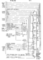
- FIGURE 1 illustrates the manner in which a monitor 9 containing the subject invention can be connected to a processor 14 being monitored (PBM), and the manner in which monitor 9 is connected to a control processor (CNT P) 10.
- Control monitor 9 controls which events are monitored in PBM and receives the data captured by monitor 9 in its main storage 19, from which the control processor can output the data onto an I/O device 20, e.g. tape or disk.
- FIGURE 3 illustrates the manner in which the invention monitors a multiprocessor (MP) system. It includes a plurality of monitors 9 respectively connected to the central processors being monitored (PBMO-PBM31. Monitors 9 are interconnected in a special way by lines Q to be able to detect which events in any PBM may have been caused by operation of another PBM and to identify the causative instruction in the other PBM.
- An MP having up to four PMBs i.e. CPO, CP1, CP2 and CP3 is disclosed and claimed in the European Patent Application 81 107 928.4, publication number 00 51 745.
- a single control processor (Ctl. P) 10 controls the operation of all monitors 9-0 through 9-3 of the MP system.
- Control processor 10 issues control commands on a single channel which is connected to each of the four monitors 9-0, 9-1, 9-2 and 9-3 which appear as I/O devices to control processor 10.
- the control processor issues sequential read commands to the four monitors so that simultaneously captured data is outputted to the channel as a related group containing the predetermined sequence of captured data from the four monitors, and the group is stored in the main storage (MS) 19 of processor 10, from which the data can be transferred to an I/O device, e.g. tape or disk if required.
- MS main storage
- each monitor a contains a monitor controller 11 which connects monitor 9 to a channel of the control processor 10, an event capture means (ECM) 12 which is connected to the PBM and captures monitored data in five byte units, a FIFO (first-in, first-outl buffer 15 which receives each five byte captured data unit immediately after it is captured, a FIFO overrun counter 15A which detects each time an event was not captured when it should have been captured, and a multirange comparator (MRC) 16 and its counters 17 which counts the number of times that captured events fall into respective predetermined address ranges.
- ECM event capture means
- MRC multirange comparator
- An OR circuit 18 connects the output data provided by the FIFO buffer 15, FIFO overrun counter 15A, or MRC counters 17 to the main storage (MS) 19 of the control processor 10 in response to an appropriate read command from processor 10 to monitor controller 15.
- the monitor controller 11 acts as an I/O control unit to decode each channel command sent to the monitor by control processor 10.
- channel commands are: (1) enable monitor, (2) set PSR (personalization register), clear and read FIFO buffer, read FIFO buffers, read counters, user defined condition (UDC), etc.
- the enable monitor command enables the addressed monitor to operate.
- the set PSR command loads a personalization register in the monitor with data for initializing a particular monitoring operation, i.e. which event will be captured, its sampling rate, other event(s) to be simultaneously monitored, etc.
- the clear and read FIFO buffer command first clears a first-in, first-out (FIFO) buffer 15 and sets the FIFO readin and readout points to FIFO location zero; and as FIFO buffer 15 receives captured data in 5 byte groups they are readout a byte at a time to the control processor main storage (MS) 19.
- the read port of the command is active for the entire measurement operation.
- the read FIFO buffer command reads out the next five byte units of captured data in the FIFO buffer 15 to MS 19 at the current FIFO readout pointer setting and increments the setting by one after the captured data unit is readout.
- the UDC command sets up the inputs to monitor 9 according to boolean conditions defined in the command to control the monitoring operation during the monitoring run. (The UDC command is not part of the subject invention.)
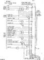
- FIGURE 2 illustrates a block diagram of the circuit contents in ECM 12 shown in FIGURE 1.
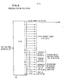
- ECM 12 is initialized for a performance measurement of the PBM by a set PSR command loading the fields in a personalization register (PSR) 24, which is shown in detail in FIGURE 8.
- PSR personalization register
- the capturable event may occur asynchronously in relation to time.
- ECM 12 When in IA mode, ECM 12 relates the occurrence of the capturable event to the instruction causing the event by generating a trigger signal to capture the associated IA value when that event happens.
- ECM 12 Upon the occurrence of each Nth capturable event, ECM 12 captures the then current instruction address, a signal indicating the on or off state at capture time of an additional event specified by PSR bits FGH, and an additional byte including the status of PBM at the time of capture.
- the captured data in this embodiment comprises four bytes for the instruction address and additional event state, and a fifth byte containing PBM status data and an indication if the FIFO buffer is then in an overrun state. If the FIFO buffer is not in an overrun state, the captured five byte data units are immediately outputted to the FIFO buffer 15 from which the captured data unit is transferred to MS 19 under a read command from the control processor 10.
- control processor cannot take the data unit from buffer 15 before the next unit is captured, the captured units are collected in buffer 15 until called for by processor 10. If FIFO buffer 15 should become full, it generates an overrun signal which prevents buffer 15 from receiving any more captured data until at least one byte is readout, which allows a byte to be received from the capture register 41 in the readout byte location. While any overrun exists, each captured data unit instead increments the FIFO overrun counter 15A.
- monitor 9 is connected to busses 13 from PBM.
- the set of signals on bus 13A represent either an instruction address (IA) or a hook (HK) as indicated by a pulse on an IA signal line or a HK signal line in bus 13A.
- An event bus 13B and a state bus 13C each have respective lines which connect to various latches and circuits in PBM to sense the occurrence of respective events or states in PBM.
- the monitor will capture certain sets of signals on bus 13A because of the occurrence of a specified event on bus 13B during program execution by PBM.
- the monitors IA or HK operating mode is determined by the one or zero output of PSR bit position 1 to a mode select circuit 26. As shown in detail in FIGURE 9, a selected IA signal or hook signal generates a bus signal on line 26A. A sequence of signals on line 26A sets a pointer flip-flop 31 to alternate its on and off outputs. Registers RA 32 and RB 33 therefore alternately receive the content of IA/HK bus 13A from the PBM in a ping-pong manner under control of the alternating outputs of pointer flip-flop 31.
- Event bus 13B comprises lines which receive the event signals from PBM listed in the following TABLE 1:
- an event capture switch (ECS) 27 receives inputs from bus 13B and also may receive capture signals Ql, Q2 and/or Q3 from other monitors if this monitor Q0 is connected in an MP.
- ECS 27 is a crosspoint type of switch which can select any of its input signals as its output signal.
- PSR bits 14-18 (designated ABCDE) are provided to ECS 27 to select one of the inputs as the capturable signal representing the capturable event.
- TABLE 2 lists the capturable events:
- Each occurrence of the selected capturable event causes a trigger signal at the output of ECS 27 which is provided to the input of a sample counter 28 and to a correlation control 29 shown in detail in FIGURE 7.
- the sampling counter 28 may be a 12-bit count-up counter. It controls the frequency of capture known as sampling rate N. Counter 28 is incremented by 1 each time ECS 27 outputs a trigger signal. The trigger signal following the sampling counter overflow will signal the correlation control 29 to capture the current instruction address and load it into a capture register 41.
- the number of trigger signals between captures is specified by N, which may be any value from 1 to 4095.
- Each Nth trigger signal outputted by ECS 27 causes the sampling counter 28 to overflow and generate a capture signal in circuit 29A which is sent to circuits 37A and 37B in FIGURE 9 which outgate the register RA or RB containing the address of the current instruction causing the selected event.
- the instruction address is transferred into bit positions 0-30 in capture register 41 in FIGURE 10.
- any of a special set of events if selected for capture, will bypass the operation of sampling counter 28 and cause a capture of the IA in register 41 on every occurrence.
- These special events are the first six events listed in TABLE 2. The remaining events in TABLE 2 are controlled by the operation of sampling counter 28.
- the PSR bits A-E are received, and the codes for the bypassed special events are sensed in circuits 29B, etc., to control the bypassing of the trigger signals via circuit 29C to activate capture flip-flop 29D which generates a capture signal that is passed through circuit 29A to control the outgating of the current IA from RA or RB to capture register 41 in FIGURE 10.
- bit position 31 is not needed for containing the IA and is used to represent the state of the additional event selected by ESS 45, because in an IBM S/370 architecture, bit 31 is not used to address instructions in the main storage since the shortest instruction is one-half word long and is addressed on one-half word boundaries (i.e. bit 301. Although bit position 31 on IA bus 30 is never used in IA mode, bit 31 may be used in hook mode. Therefore, in IA mode, position 31 in capture register 41 is used to record the state of the event selected by ESS 45 at each capture time, and bit 31 may represent the state of any event selected by PSR bits FGH in the following TABLE 5:
- ESS 45 also is a crosspoint type of switch.
- the combinatorial state of bits FGH selects one of the PBM inputs to ESS 45 as its output to bit position 31 in register 41. Therefore, bit position 31 in register 41 may be either one or zero with a captured IA.
- a capture valid (CV) flip/flop 43 is set.
- the CV signals the FIFO buffer 15 that byte 0 is being outputted from capture register 41 to buffer 15.
- a return signal from FIFO is provided to an outgate control 42 to cause the next captured byte to be outgated from register 47. This sequence is repeated until all five bytes are transferred to the FIFO buffer.
- CV flip flop 43 is reset. Register 41 is now ready to capture another instruction address.
- sampling counter 28 While register 41 is busy outgating its contents, the sampling counter 28 continues counting trigger pulses received from ECS 27. If sampling counter 28 overflows while the capture register 41 is outgating, sampling counter 28 is again loaded from the PSR with its count value; but instead of an IA capture occuring on such overflow, a capture overrun signal is raised to increment a capture overrun counter 46.
- the maximum rate at which the captures can occur is dependent on the execution rate of the PBM; the faster its execution rate, the sooner the next capture can occur.
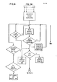
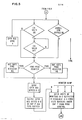
- the monitor operation is summarized by the flow diagrams shown in FIGURES 4 and 5.
- FIGURE 6 through 11 the same reference numbers are used for identical components as in the FIGURES 1 through 3. Some components are divided in subcomponents which are referenced by suffixes A, B, C, ... together with the related component reference number.
Abstract
Description
- The subject invention relates to hardware monitors for generating measurement data on the performance characteristics of data processing systems.
- Many computer performance monitoring tools have been developed in the prior art for the purpose of evaluating computer systems. Most have been conceived with different goals in mind. Some of these tools are software, some hardware; many of the hardware measurement devices require program analysis of their output, and some of the software tools require input data that is collected by one of the hardware devices.
- All monitors can basically be divided into two categories; counters and recorders. The counter counts the number of occurrences of an event and the counter output usually represents some kind of meaningful information. The recorder, on the other hand, collects data about a defined event on some recording media for later processing to
- make the data meaningful. Most generally, the recorder is used when the event to be analyzed is of a complex nature. Tracing programs can perform the recorder type of monitoring. Known counter type monitors usually monitor six mutually exclusive states in a processor, which were:
- 1. Total operation time,
- 2. Channel A operation time,
- 3. Channel B operation time,
- 4. CPU operation time, no I/O in process,
- 5. Tape equipment operation time, CPU in wait state.
- 6. Card equipment operation time, CPU in wait state.
- Software monitors and tracing programs universally have the problem of distorting the processor operations which they are measuring, because they compete for some of the same system resources.
- All monitoring functions also fall into two classes: those that sense hooks specially put into the code to assist a monitoring operation, and those that sense some characteristic of a program provided to perform the program's function. Hooks are special instructions inserted into the code for reasuring purposes. The monitor call (MC) instruction in the IBM System/370 architecture is provided for use as a hook in program code. For example, a hook may be put into a routine or queue, so that the number of times such hook instruction executes can be counted to determine the number of times that the routine or queue is entered by a program. A hardware monitor has been used to sense and count the occurrence of a hook instruction. Monitor functions which have been used to sense non-hook program characteristics, for example, have sensed the frequency of occurrence of specified instruction operation coded and the address distribution of requests to main storage.
- Background on monitors and their use is described in a book entitled "Evaluation and Measurement Techniques for Digital Computer Systems" by M. E. Drummond, Jr. published in 1973 by Prentice-Hall, Inc., Inglewood Cliffs, New Jersey.
- Examples of patents on data processing system hardware monitors which use counters as an output entity are represented by US-PS 3,399,298 US-PS 3,588,837 and US-PS 4,068,304.
- It is therefore the principle task of this invention to provide a hardware monitor which is capable of relating the occurrence of asynchronous hardware events to a causative software event, as represented by the address of the causative instruction in an instruction stream of a data processing system, which may be a multiprocessor system, without distorting the processor operations monitored.
- The features to achieve this task are characterized by
claim 1. The other claims show advantageous arrangements and developments of the invention. - The invention advantageously enables novel monitoring activities, such as: determining which instruction is the cause of a system deadlock in an MP, correlating software events occurring in plural processors of an MP, correlating hardware interactions within an MP in relation to software being performed in the different central processors comprising the MP. Characteristics monitored for single processors include being able to determine: the cache miss or hit rate for a processor, determining which instruction caused the accessing of a particular operand address, indicating the state of a processor at the time that a monitored event occurred, being able to record information indicating that the monitored information is not valid and should be ignored in determining processor operation results.
- It is another advantage of this invention to provide a hardware monitor to capture and record data of a very high speed processor which has an instruction rate that is equal or greater than the capture and recording rate of the monitor by having the monitor sample the nth occurrence of the event. It has been found statistically that over a relatively large number of occurrences of an event being monitored that the measurement accuracy of the monitor results is virtually the same as if all occurrences of the monitored event had been captured and recorded. The result is that the monitor can monitor a processor having n times the instruction rate that a non-sampling type of mcnitor could handle, and with resulting economics in the choice of circuit speeds necessary to build the monitor. The choice of a minimum value for the sampling rate n is done with the use of a recording buffer overrun counter, wherein n is increased until the overrun rate is very small or zero.
- It is a further advantage of this invention to enable data to be collected from numerous software environments, including application programs and different operating systems, without the necessity of providing special hooks or other markers or modifications into the code to disturb the code which may make more difficult the obtaining of statistical information on the operation of the code.
- One way of carrying out the invention is described in detail below with reference to drawings which show a preferred embodiment of the invention.
- Fig. 1 shows a general block diagram of a monitor containing the subject invention and its connections between a processor being monitored (PBM) and a control processor (CNT P) which controls the operation of the monitor.
- Fig. 2 is a general block diagram of the internal circuit arrangement within a preferred embodiment of the subject invention.
- Fig. 3 illustrates a preferred embodiment of the invention involving a plurality of monitors connected to respective processors being monitored in a multiprocessor (MP) system.
- Figs. 4 are flow diagrams illustrating a summary and 5 of the operation of the invention.
- Figs. 6 illustrate detailed circuit diagrams used through 11 in the preferred embodiment.
- The monitor described herein correlates software activity to hardware activity by capturing samples of instruction addresses (which are architecturally visable to the software) causing the occurrence of the monitored hardware activity manifested by electrical signals in a processor circuit (e.g. setting of a latch), and recording the instruction addresses with a designation of the monitored hardware activity (e.g. a DLAT reference or cache misses). The invention makes possible the monitoring of software and/or hardware relationships between processors in a multiprocessor by connecting a monitor to each processor being monitored, and interconnecting an event capture signal generated in one processor monitor (master) to control the capture recording means in another processor monitor (slave), so that the recorded information can indicate if the instruction in one processor is responsible for the event occurring in the other processor. This MP monitor connection requires that the event sampling function be whenever it receives an event capture signal from the master monitor. In this manner, monitor can be made the master and any monitor can be made the slave according to the processor interrelationship being monitored. The MP monitoring requires a sequenced outputting of the captured data in the plural monitors of the MP, which is done under control of a control processor that records the captured data with a designated sequence. The output sequencing with the monitored processor identifier in the data items enables the MP interrelationships to be determined. Thus, the subject invention enables a monitor to determine uniprocessor characteristics such as operand reference rate, and cache reference rate, and to determine multiprocessor characteristics such as interprocessor cache cross-interrogation behavior and interprocessor deadlock causes.
- At the beginning of a monitor data collection operation, a personalization register in each monitor is loaded by the control processor with the identifier of the processor being monitored (PBM), the sample count value N, a designation of the particular hardware event in PBM which is the capturable event which is to control the capture of its causative instruction address, and second event designation of an event or condition whose current state will be indicated as part of the captured data. The values loaded into the personalization register are provided by the user in a program in the control processor which loads the register.
- Then a sampling counter is set to that sampling value N to control the sampling rate of the designated capture event; N may be set to any value from 1 to a large number such as 1,000,000. If N is set to 1, every occurrence of the designated capture event is being monitored. For example, if N is set to 1,000 then only every thousandth occurrence of the event is monitored.
- A cross-bar type of switch is provided to enable selection of the capturable event designated by the personalization register among plural capturable signals provided by PBM to the monitor. The output of this switch drives the sampling counter.
- A second cross-bar type of switch is controlled by the second event designation from the personalization register to select the second event from the plurality of signals provided by PBM to the monitor.
- A correlation control receives PBM signals indicating the occurrence of the selected capturable event, receives the address of each instruction executing in the PBM from the PBM instruction address register, and receives the sampling count signals from which a capture signal is generated to indicate the occurrence of each Nth capturable event, which will correlate with the instruction in the program causing the Nth capturable event.
- A capture register is enabled by the capture signal to store the address of the instruction which caused the event, along with the states of other selected signals existing at the time of capture. Also, the PBM identifier, and designators of the captured event and any selected additional event are also stored in the capture register at the time of capture to enhance the information content of the captured data, which is transferred to a FIFO output buffer.
- The control processor reads the data in the output buffer in the order the data is generated, and the control processor may store the data on an I/O device. The control processor readout rate from the monitor is coordinated with the monitor sampling rate N, when it is desired to use the lowest sampling rate N consistent with accurate PBM performance data.
- FIGURE 1 illustrates the manner in which a
monitor 9 containing the subject invention can be connected to aprocessor 14 being monitored (PBM), and the manner in which monitor 9 is connected to a control processor (CNT P) 10. Control monitor 9 controls which events are monitored in PBM and receives the data captured bymonitor 9 in itsmain storage 19, from which the control processor can output the data onto an I/O device 20, e.g. tape or disk. - FIGURE 3 illustrates the manner in which the invention monitors a multiprocessor (MP) system. It includes a plurality of
monitors 9 respectively connected to the central processors being monitored (PBMO-PBM31.Monitors 9 are interconnected in a special way by lines Q to be able to detect which events in any PBM may have been caused by operation of another PBM and to identify the causative instruction in the other PBM. An MP having up to four PMBs (i.e. CPO, CP1, CP2 and CP3) is disclosed and claimed in the European Patent Application 81 107 928.4,publication number 00 51 745. - A single control processor (Ctl. P) 10 controls the operation of all monitors 9-0 through 9-3 of the MP system.
Control processor 10 issues control commands on a single channel which is connected to each of the four monitors 9-0, 9-1, 9-2 and 9-3 which appear as I/O devices to controlprocessor 10. The control processor issues sequential read commands to the four monitors so that simultaneously captured data is outputted to the channel as a related group containing the predetermined sequence of captured data from the four monitors, and the group is stored in the main storage (MS) 19 ofprocessor 10, from which the data can be transferred to an I/O device, e.g. tape or disk if required. - As shown in FIGURE 1, each monitor a contains a
monitor controller 11 which connectsmonitor 9 to a channel of thecontrol processor 10, an event capture means (ECM) 12 which is connected to the PBM and captures monitored data in five byte units, a FIFO (first-in, first-outl buffer 15 which receives each five byte captured data unit immediately after it is captured, aFIFO overrun counter 15A which detects each time an event was not captured when it should have been captured, and a multirange comparator (MRC) 16 and itscounters 17 which counts the number of times that captured events fall into respective predetermined address ranges. This invention is primarily concerned withECM 12,FIFO buffer 15 andFIFO overrun counter 15A and not with MRC16 and itscounters 17. - An OR
circuit 18 connects the output data provided by theFIFO buffer 15,FIFO overrun counter 15A, or MRC counters 17 to the main storage (MS) 19 of thecontrol processor 10 in response to an appropriate read command fromprocessor 10 to monitorcontroller 15. - The
monitor controller 11 acts as an I/O control unit to decode each channel command sent to the monitor bycontrol processor 10. Among the available channel commands are: (1) enable monitor, (2) set PSR (personalization register), clear and read FIFO buffer, read FIFO buffers, read counters, user defined condition (UDC), etc. - The enable monitor command enables the addressed monitor to operate. The set PSR command loads a personalization register in the monitor with data for initializing a particular monitoring operation, i.e. which event will be captured, its sampling rate, other event(s) to be simultaneously monitored, etc. The clear and read FIFO buffer command first clears a first-in, first-out (FIFO)
buffer 15 and sets the FIFO readin and readout points to FIFO location zero; and asFIFO buffer 15 receives captured data in 5 byte groups they are readout a byte at a time to the control processor main storage (MS) 19. The read port of the command is active for the entire measurement operation. On the other hand the read FIFO buffer command reads out the next five byte units of captured data in theFIFO buffer 15 toMS 19 at the current FIFO readout pointer setting and increments the setting by one after the captured data unit is readout. The UDC command sets up the inputs to monitor 9 according to boolean conditions defined in the command to control the monitoring operation during the monitoring run. (The UDC command is not part of the subject invention.) - FIGURE 2 illustrates a block diagram of the circuit contents in
ECM 12 shown in FIGURE 1.ECM 12 is initialized for a performance measurement of the PBM by a set PSR command loading the fields in a personalization register (PSR) 24, which is shown in detail in FIGURE 8. The set PSR command loads: - (1)
PSR bit position 1 to select the mode of operation formonitor 9 as either the instruction address (IA) mode, or the hook (HK) mode. (The invention claimed in this specification relates to the IA mcde of operation.) - (2) PSR bit positions 2-13 receive a sample count number N.
- (3) PSR bit positions 14-18 (labeled A-E) select the capturable event.
- (41 PSR bit positions 19-21 (labeled FGH) select an additional event whose state is captured whenever the capturable event is captured and may be for an event other than the capturable event; and
- (5) PSR bit positions 21 and 22 (labeled Ll and L2) identify the processor being monitored.
- The capturable event may occur asynchronously in relation to time. When in IA mode,
ECM 12 relates the occurrence of the capturable event to the instruction causing the event by generating a trigger signal to capture the associated IA value when that event happens. - Upon the occurrence of each Nth capturable event,
ECM 12 captures the then current instruction address, a signal indicating the on or off state at capture time of an additional event specified by PSR bits FGH, and an additional byte including the status of PBM at the time of capture. The captured data in this embodiment comprises four bytes for the instruction address and additional event state, and a fifth byte containing PBM status data and an indication if the FIFO buffer is then in an overrun state. If the FIFO buffer is not in an overrun state, the captured five byte data units are immediately outputted to theFIFO buffer 15 from which the captured data unit is transferred toMS 19 under a read command from thecontrol processor 10. If the control processor cannot take the data unit frombuffer 15 before the next unit is captured, the captured units are collected inbuffer 15 until called for byprocessor 10. IfFIFO buffer 15 should become full, it generates an overrun signal which preventsbuffer 15 from receiving any more captured data until at least one byte is readout, which allows a byte to be received from thecapture register 41 in the readout byte location. While any overrun exists, each captured data unit instead increments theFIFO overrun counter 15A. - As shown in FIGURE 1, monitor 9 is connected to
busses 13 from PBM. The set of signals onbus 13A represent either an instruction address (IA) or a hook (HK) as indicated by a pulse on an IA signal line or a HK signal line inbus 13A. An event bus 13B and astate bus 13C each have respective lines which connect to various latches and circuits in PBM to sense the occurrence of respective events or states in PBM. The monitor will capture certain sets of signals onbus 13A because of the occurrence of a specified event on bus 13B during program execution by PBM. - The monitors IA or HK operating mode is determined by the one or zero output of
PSR bit position 1 to a modeselect circuit 26. As shown in detail in FIGURE 9, a selected IA signal or hook signal generates a bus signal online 26A. A sequence of signals online 26A sets a pointer flip-flop 31 to alternate its on and off outputs.Registers RA 32 andRB 33 therefore alternately receive the content of IA/HK bus 13A from the PBM in a ping-pong manner under control of the alternating outputs of pointer flip-flop 31. - Event bus 13B comprises lines which receive the event signals from PBM listed in the following TABLE 1:

- In FIGURE 2, an event capture switch (ECS) 27 receives inputs from bus 13B and also may receive capture signals Ql, Q2 and/or Q3 from other monitors if this monitor Q0 is connected in an MP.
ECS 27 is a crosspoint type of switch which can select any of its input signals as its output signal. PSR bits 14-18 (designated ABCDE) are provided toECS 27 to select one of the inputs as the capturable signal representing the capturable event. The following TABLE 2 lists the capturable events:
- Each occurrence of the selected capturable event causes a trigger signal at the output of
ECS 27 which is provided to the input of asample counter 28 and to acorrelation control 29 shown in detail in FIGURE 7. Thesampling counter 28 may be a 12-bit count-up counter. It controls the frequency of capture known as samplingrate N. Counter 28 is incremented by 1 eachtime ECS 27 outputs a trigger signal. The trigger signal following the sampling counter overflow will signal thecorrelation control 29 to capture the current instruction address and load it into acapture register 41. The number of trigger signals between captures is specified by N, which may be any value from 1 to 4095. Each Nth trigger signal outputted byECS 27 causes thesampling counter 28 to overflow and generate a capture signal incircuit 29A which is sent tocircuits 37A and 37B in FIGURE 9 which outgate the register RA or RB containing the address of the current instruction causing the selected event. The instruction address is transferred into bit positions 0-30 in capture register 41 in FIGURE 10. - However, any of a special set of events, if selected for capture, will bypass the operation of
sampling counter 28 and cause a capture of the IA inregister 41 on every occurrence. These special events are the first six events listed in TABLE 2. The remaining events in TABLE 2 are controlled by the operation ofsampling counter 28. In FIGURE 7, the PSR bits A-E are received, and the codes for the bypassed special events are sensed in circuits 29B, etc., to control the bypassing of the trigger signals via circuit 29C to activate capture flip-flop 29D which generates a capture signal that is passed throughcircuit 29A to control the outgating of the current IA from RA or RB to captureregister 41 in FIGURE 10. - Whenever a capture signal ingates an IA into
capture register 41, the states of an additional event selected by abit 31 eventselect switch 45 may also be captured inregister 41 with the IA. At the same time, certain PBM states onbus 13C are loaded into the fifth byte (byte 4, bits 32-35) incapture register 41. Also the PBM identifier Ll, L2 is loaded intobyte 4,bits 
- In IA mode,
bit position 31 is not needed for containing the IA and is used to represent the state of the additional event selected byESS 45, because in an IBM S/370 architecture,bit 31 is not used to address instructions in the main storage since the shortest instruction is one-half word long and is addressed on one-half word boundaries (i.e. bit 301. Althoughbit position 31 onIA bus 30 is never used in IA mode,bit 31 may be used in hook mode. Therefore, in IA mode,position 31 incapture register 41 is used to record the state of the event selected byESS 45 at each capture time, and bit 31 may represent the state of any event selected by PSR bits FGH in the following TABLE 5:
-
ESS 45 also is a crosspoint type of switch. The combinatorial state of bits FGH selects one of the PBM inputs toESS 45 as its output to bitposition 31 inregister 41. Therefore,bit position 31 inregister 41 may be either one or zero with a captured IA. - Once the content of RA or RB is transferred to capture
register 41, the capture is complete and a capture valid (CV) flip/flop 43 is set. The CV signals theFIFO buffer 15 thatbyte 0 is being outputted from capture register 41 to buffer 15. A return signal from FIFO is provided to anoutgate control 42 to cause the next captured byte to be outgated from register 47. This sequence is repeated until all five bytes are transferred to the FIFO buffer. At the end of the fifth byte transfer,CV flip flop 43 is reset.Register 41 is now ready to capture another instruction address. - While
register 41 is busy outgating its contents, thesampling counter 28 continues counting trigger pulses received fromECS 27. If sampling counter 28 overflows while thecapture register 41 is outgating, samplingcounter 28 is again loaded from the PSR with its count value; but instead of an IA capture occuring on such overflow, a capture overrun signal is raised to increment a capture overruncounter 46. The maximum rate at which the captures can occur is dependent on the execution rate of the PBM; the faster its execution rate, the sooner the next capture can occur. - The monitor operation is summarized by the flow diagrams shown in FIGURES 4 and 5.
- In view of the preceding description, the detailed hardware logic diagrams of the preferred embodiment of this invention shown in FIGURES 6 through 11 will be understood by anyone skilled in the art of making and using related types of machines.
- In FIGURE 6 through 11 the same reference numbers are used for identical components as in the FIGURES 1 through 3. Some components are divided in subcomponents which are referenced by suffixes A, B, C, ... together with the related component reference number.
Claims (21)
Applications Claiming Priority (2)
| Application Number | Priority Date | Filing Date | Title |
|---|---|---|---|
| US06/273,530 US4435759A (en) | 1981-06-15 | 1981-06-15 | Hardware monitor for obtaining processor software/hardware interrelationships |
| US273530 | 1981-06-15 |
Publications (3)
| Publication Number | Publication Date |
|---|---|
| EP0067324A2 true EP0067324A2 (en) | 1982-12-22 |
| EP0067324A3 EP0067324A3 (en) | 1985-03-27 |
| EP0067324B1 EP0067324B1 (en) | 1988-11-23 |
Family
ID=23044320
Family Applications (1)
| Application Number | Title | Priority Date | Filing Date |
|---|---|---|---|
| EP82104510A Expired EP0067324B1 (en) | 1981-06-15 | 1982-05-24 | Software correlating hardware monitor system |
Country Status (4)
| Country | Link |
|---|---|
| US (1) | US4435759A (en) |
| EP (1) | EP0067324B1 (en) |
| JP (1) | JPS57211655A (en) |
| DE (1) | DE3279236D1 (en) |
Cited By (5)
| Publication number | Priority date | Publication date | Assignee | Title |
|---|---|---|---|---|
| EP0094623A1 (en) * | 1982-05-14 | 1983-11-23 | Siemens Aktiengesellschaft | Circuit for telecommunication exchanges, especially telephone switching exchanges, with multiprocessor systems for call processing purposes |
| EP0130469A2 (en) * | 1983-06-29 | 1985-01-09 | International Business Machines Corporation | Internally distributed monitoring system |
| EP0198568A2 (en) * | 1985-04-15 | 1986-10-22 | Control Data Corporation | Data capture logic system |
| FR2591364A1 (en) * | 1985-12-05 | 1987-06-12 | Mary Joel | Device for evaluation, by measurement, of the performance of a computer system |
| EP0257241A2 (en) * | 1986-08-15 | 1988-03-02 | International Business Machines Corporation | Internal computer performance monitoring by event sampling |
Families Citing this family (54)
| Publication number | Priority date | Publication date | Assignee | Title |
|---|---|---|---|---|
| US4485440A (en) * | 1981-09-24 | 1984-11-27 | At&T Bell Laboratories | Central processor utilization monitor |
| US4598364A (en) * | 1983-06-29 | 1986-07-01 | International Business Machines Corporation | Efficient trace method adaptable to multiprocessors |
| US4638427A (en) * | 1984-04-16 | 1987-01-20 | International Business Machines Corporation | Performance evaluation for an asymmetric multiprocessor system |
| US5263153A (en) * | 1987-01-22 | 1993-11-16 | National Semiconductor Corporation | Monitoring control flow in a microprocessor |
| EP0325421B1 (en) * | 1988-01-20 | 1994-08-10 | Advanced Micro Devices, Inc. | Organization of an integrated cache unit for flexible usage in supporting multiprocessor operations |
| US5113518A (en) * | 1988-06-03 | 1992-05-12 | Durst Jr Robert T | Method and system for preventing unauthorized use of software |
| US5287511A (en) * | 1988-07-11 | 1994-02-15 | Star Semiconductor Corporation | Architectures and methods for dividing processing tasks into tasks for a programmable real time signal processor and tasks for a decision making microprocessor interfacing therewith |
| US5263143A (en) * | 1988-07-11 | 1993-11-16 | Star Semiconductor Corporation | Real time probe device for internals of signal processor |
| JPH02199548A (en) * | 1988-11-09 | 1990-08-07 | Asea Brown Boveri Ag | Observing method for development with the lapse of time of object program made by electronic computer system and observation instrument practicing said method |
| US5465258A (en) * | 1989-11-13 | 1995-11-07 | Integrity Systems, Inc. | Binary image performance evaluation tool |
| US5551050A (en) * | 1989-12-20 | 1996-08-27 | Texas Instruments Incorporated | System and method using synchronized processors to perform real time internal monitoring of a data processing device |
| US5121501A (en) * | 1989-12-27 | 1992-06-09 | International Business Machines Corporation | First processor inserting hooks into software and sending unique identifications to output bus and second processor associating data frames and time with these unique identifications |
| EP0530310A4 (en) * | 1990-05-18 | 1993-07-21 | Star Semiconductor Corporation | Programmable signal processor architecture |
| WO1992005496A1 (en) * | 1990-09-17 | 1992-04-02 | Star Semiconductor Corporation | Event signalling system and method for processor system having central memory unit |
| US5361355A (en) * | 1991-02-08 | 1994-11-01 | Fujitsu Limited | Software asset systemizer |
| US5426741A (en) * | 1991-02-20 | 1995-06-20 | Digital Equipment Corporation | Bus event monitor |
| JPH0816877B2 (en) * | 1991-06-10 | 1996-02-21 | インターナショナル・ビジネス・マシーンズ・コーポレイション | Method and system for real-time capture and reduction of resource data for data processing system |
| AU2374492A (en) * | 1991-07-22 | 1993-02-23 | Banyan Systems Incorporated | System bus monitor for compiling data regarding use of a system bus |
| US5418930A (en) * | 1991-09-05 | 1995-05-23 | International Business Machines Corporation | Circuit for interfacing asynchronous to synchronous communications |
| US5450349A (en) * | 1992-10-27 | 1995-09-12 | Digital Equipment Corporation | Computer system performance evaluation system and method |
| US5452457A (en) * | 1993-01-29 | 1995-09-19 | International Business Machines Corporation | Program construct and methods/systems for optimizing assembled code for execution |
| WO1995016969A1 (en) * | 1993-12-15 | 1995-06-22 | Supercomm, Inc. | Database versioning with output only of data changed from the previous version |
| US5537541A (en) * | 1994-08-16 | 1996-07-16 | Digital Equipment Corporation | System independent interface for performance counters |
| JP2908739B2 (en) * | 1994-12-16 | 1999-06-21 | インターナショナル・ビジネス・マシーンズ・コーポレイション | System and method for monitoring a CPU in a multiprocessor system |
| US6021457A (en) * | 1995-09-28 | 2000-02-01 | Intel Corporation | Method and an apparatus for minimizing perturbation while monitoring parallel applications |
| US5949971A (en) * | 1995-10-02 | 1999-09-07 | International Business Machines Corporation | Method and system for performance monitoring through identification of frequency and length of time of execution of serialization instructions in a processing system |
| US5729726A (en) * | 1995-10-02 | 1998-03-17 | International Business Machines Corporation | Method and system for performance monitoring efficiency of branch unit operation in a processing system |
| US5752062A (en) * | 1995-10-02 | 1998-05-12 | International Business Machines Corporation | Method and system for performance monitoring through monitoring an order of processor events during execution in a processing system |
| US5691920A (en) * | 1995-10-02 | 1997-11-25 | International Business Machines Corporation | Method and system for performance monitoring of dispatch unit efficiency in a processing system |
| US5748855A (en) * | 1995-10-02 | 1998-05-05 | Iinternational Business Machines Corporation | Method and system for performance monitoring of misaligned memory accesses in a processing system |
| US5797019A (en) * | 1995-10-02 | 1998-08-18 | International Business Machines Corporation | Method and system for performance monitoring time lengths of disabled interrupts in a processing system |
| US5751945A (en) * | 1995-10-02 | 1998-05-12 | International Business Machines Corporation | Method and system for performance monitoring stalls to identify pipeline bottlenecks and stalls in a processing system |
| US5968188A (en) | 1998-03-10 | 1999-10-19 | Grammar Engine | System for providing real-time code coverage |
| US6134676A (en) * | 1998-04-30 | 2000-10-17 | International Business Machines Corporation | Programmable hardware event monitoring method |
| US6370659B1 (en) | 1999-04-22 | 2002-04-09 | Harris Corporation | Method for automatically isolating hardware module faults |
| US6460107B1 (en) | 1999-04-29 | 2002-10-01 | Intel Corporation | Integrated real-time performance monitoring facility |
| US6611926B1 (en) * | 1999-11-29 | 2003-08-26 | Hewlett-Packard Development Company, L.P. | Mechanisms to sample shared-dirty-line addresses |
| US6748558B1 (en) * | 2000-05-10 | 2004-06-08 | Motorola, Inc. | Performance monitor system and method suitable for use in an integrated circuit |
| US6542844B1 (en) * | 2000-08-02 | 2003-04-01 | International Business Machines Corporation | Method and apparatus for tracing hardware states using dynamically reconfigurable test circuits |
| US20020073406A1 (en) * | 2000-12-12 | 2002-06-13 | Darryl Gove | Using performance counter profiling to drive compiler optimization |
| WO2004010645A1 (en) * | 2002-07-18 | 2004-01-29 | Vega Grieshaber Kg | Bus station with an integrated bus monitor function |
| GB2393272A (en) * | 2002-09-19 | 2004-03-24 | Advanced Risc Mach Ltd | Controlling performance counters within a data processing system |
| US7451459B2 (en) * | 2003-05-05 | 2008-11-11 | Microsoft Corporation | Systems, methods, and apparatus for indicating processor hierarchical topology |
| US7165145B2 (en) * | 2003-07-02 | 2007-01-16 | Falconstor Software, Inc. | System and method to protect data stored in a storage system |
| US7334114B2 (en) * | 2005-05-16 | 2008-02-19 | Texas Instruments Incorporated | Real-time monitoring, alignment, and translation of CPU stalls or events |
| US8516226B1 (en) * | 2006-01-23 | 2013-08-20 | Hewlett-Packard Development Company, L.P. | Executing a prefetching policy responsive to entry into an execution phase of an application |
| US7873534B2 (en) * | 2006-02-14 | 2011-01-18 | Microsoft Corporation | Collecting CRM data for feedback |
| US8656411B2 (en) * | 2008-03-05 | 2014-02-18 | Intel Corporation | Technique for monitoring activity within an integrated circuit |
| US20100008464A1 (en) * | 2008-07-11 | 2010-01-14 | Infineon Technologies Ag | System profiling |
| US9032375B2 (en) * | 2011-04-27 | 2015-05-12 | International Business Machines Corporation | Performance bottleneck identification tool |
| WO2015088534A1 (en) * | 2013-12-12 | 2015-06-18 | Intel Corporation | Techniques for detecting race conditions |
| US9454424B2 (en) | 2014-08-27 | 2016-09-27 | Freescale Semiconductor, Inc. | Methods and apparatus for detecting software inteference |
| DE102015217074A1 (en) * | 2015-09-07 | 2017-03-09 | Siemens Aktiengesellschaft | Method and device for dynamic correctness analysis of software |
| US10732852B1 (en) * | 2017-10-19 | 2020-08-04 | EMC IP Holding Company LLC | Telemetry service |
Citations (3)
| Publication number | Priority date | Publication date | Assignee | Title |
|---|---|---|---|---|
| US4166290A (en) * | 1978-05-10 | 1979-08-28 | Tesdata Systems Corporation | Computer monitoring system |
| US4241416A (en) * | 1977-07-01 | 1980-12-23 | Systron-Donner Corporation | Monitoring apparatus for processor controlled equipment |
| US4250562A (en) * | 1979-05-22 | 1981-02-10 | Hewlett-Packard Company | Digital signal state analyzer and display |
Family Cites Families (1)
| Publication number | Priority date | Publication date | Assignee | Title |
|---|---|---|---|---|
| US3818458A (en) | 1972-11-08 | 1974-06-18 | Comress | Method and apparatus for monitoring a general purpose digital computer |
-
1981
- 1981-06-15 US US06/273,530 patent/US4435759A/en not_active Expired - Fee Related
-
1982
- 1982-05-24 DE DE8282104510T patent/DE3279236D1/en not_active Expired
- 1982-05-24 EP EP82104510A patent/EP0067324B1/en not_active Expired
- 1982-06-15 JP JP57101485A patent/JPS57211655A/en active Pending
Patent Citations (3)
| Publication number | Priority date | Publication date | Assignee | Title |
|---|---|---|---|---|
| US4241416A (en) * | 1977-07-01 | 1980-12-23 | Systron-Donner Corporation | Monitoring apparatus for processor controlled equipment |
| US4166290A (en) * | 1978-05-10 | 1979-08-28 | Tesdata Systems Corporation | Computer monitoring system |
| US4250562A (en) * | 1979-05-22 | 1981-02-10 | Hewlett-Packard Company | Digital signal state analyzer and display |
Non-Patent Citations (1)
| Title |
|---|
| IBM TECHNICAL DISCLOSURE BULLETIN, vol. 22, no. 7, December 1979, pages 2651-2654, New York, US; W.J. BROWN et al.: "Circuit for tracing branch instructions" * |
Cited By (8)
| Publication number | Priority date | Publication date | Assignee | Title |
|---|---|---|---|---|
| EP0094623A1 (en) * | 1982-05-14 | 1983-11-23 | Siemens Aktiengesellschaft | Circuit for telecommunication exchanges, especially telephone switching exchanges, with multiprocessor systems for call processing purposes |
| EP0130469A2 (en) * | 1983-06-29 | 1985-01-09 | International Business Machines Corporation | Internally distributed monitoring system |
| EP0130469A3 (en) * | 1983-06-29 | 1987-10-14 | International Business Machines Corporation | Internally distributed monitoring system |
| EP0198568A2 (en) * | 1985-04-15 | 1986-10-22 | Control Data Corporation | Data capture logic system |
| EP0198568A3 (en) * | 1985-04-15 | 1989-03-22 | Control Data Corporation | Data capture logic system |
| FR2591364A1 (en) * | 1985-12-05 | 1987-06-12 | Mary Joel | Device for evaluation, by measurement, of the performance of a computer system |
| EP0257241A2 (en) * | 1986-08-15 | 1988-03-02 | International Business Machines Corporation | Internal computer performance monitoring by event sampling |
| EP0257241A3 (en) * | 1986-08-15 | 1990-01-17 | International Business Machines Corporation | Internal computer performance monitoring by event sampling |
Also Published As
| Publication number | Publication date |
|---|---|
| EP0067324A3 (en) | 1985-03-27 |
| JPS57211655A (en) | 1982-12-25 |
| US4435759A (en) | 1984-03-06 |
| DE3279236D1 (en) | 1988-12-29 |
| EP0067324B1 (en) | 1988-11-23 |
Similar Documents
| Publication | Publication Date | Title |
|---|---|---|
| EP0067324B1 (en) | Software correlating hardware monitor system | |
| US4821178A (en) | Internal performance monitoring by event sampling | |
| US8978017B2 (en) | Profiling operating context | |
| US5151981A (en) | Instruction sampling instrumentation | |
| EP0130469B1 (en) | Internally distributed monitoring system | |
| US5608866A (en) | System for measuring and analyzing operation of information processor | |
| CA1123106A (en) | Computer monitoring system | |
| US4367525A (en) | CPU Channel monitoring system | |
| US8141053B2 (en) | Call stack sampling using a virtual machine | |
| US6539500B1 (en) | System and method for tracing | |
| US5835702A (en) | Performance monitor | |
| KR100280732B1 (en) | Performance monitoring method and apparatus of data processing system | |
| US3540003A (en) | Computer monitoring system | |
| US4503495A (en) | Data processing system common bus utilization detection logic | |
| US5193179A (en) | Activity monitor system non-obtrusive statistical monitoring of operations on a shared bus of a multiprocessor system | |
| US5675729A (en) | Method and apparatus for performing on-chip measurement on a component | |
| US4949252A (en) | Computer channel analyzer with monitoring and selective display of predetermining events and related data | |
| US5920689A (en) | System and method for low overhead, high precision performance measurements using state transitions | |
| EP0076921B1 (en) | Method and system for time measurements of data processing channels | |
| US3723975A (en) | Overdue event detector | |
| US7225105B2 (en) | Extending width of performance monitor counters | |
| US4773003A (en) | Apparatus for monitoring and analyzing large data blocks on a computer channel | |
| US7072813B2 (en) | Mechanism to synchronize probes during simulation of system-level designs | |
| JP2834194B2 (en) | Hardware monitor | |
| KR20040043119A (en) | Method and apparatus for gathering queue performance data |
Legal Events
| Date | Code | Title | Description |
|---|---|---|---|
| PUAI | Public reference made under article 153(3) epc to a published international application that has entered the european phase |
Free format text: ORIGINAL CODE: 0009012 |
|
| AK | Designated contracting states |
Designated state(s): DE FR GB IT |
|
| 17P | Request for examination filed |
Effective date: 19830420 |
|
| PUAL | Search report despatched |
Free format text: ORIGINAL CODE: 0009013 |
|
| AK | Designated contracting states |
Designated state(s): DE FR GB IT |
|
| 17Q | First examination report despatched |
Effective date: 19860506 |
|
| GRAA | (expected) grant |
Free format text: ORIGINAL CODE: 0009210 |
|
| AK | Designated contracting states |
Kind code of ref document: B1 Designated state(s): DE FR GB IT |
|
| PG25 | Lapsed in a contracting state [announced via postgrant information from national office to epo] |
Ref country code: IT Free format text: LAPSE BECAUSE OF FAILURE TO SUBMIT A TRANSLATION OF THE DESCRIPTION OR TO PAY THE FEE WITHIN THE PRESCRIBED TIME-LIMIT;WARNING: LAPSES OF ITALIAN PATENTS WITH EFFECTIVE DATE BEFORE 2007 MAY HAVE OCCURRED AT ANY TIME BEFORE 2007. THE CORRECT EFFECTIVE DATE MAY BE DIFFERENT FROM THE ONE RECORDED. Effective date: 19881123 |
|
| REF | Corresponds to: |
Ref document number: 3279236 Country of ref document: DE Date of ref document: 19881229 |
|
| ET | Fr: translation filed | ||
| PGFP | Annual fee paid to national office [announced via postgrant information from national office to epo] |
Ref country code: FR Payment date: 19890426 Year of fee payment: 8 |
|
| PGFP | Annual fee paid to national office [announced via postgrant information from national office to epo] |
Ref country code: GB Payment date: 19890430 Year of fee payment: 8 |
|
| PLBE | No opposition filed within time limit |
Free format text: ORIGINAL CODE: 0009261 |
|
| STAA | Information on the status of an ep patent application or granted ep patent |
Free format text: STATUS: NO OPPOSITION FILED WITHIN TIME LIMIT |
|
| 26N | No opposition filed | ||
| PG25 | Lapsed in a contracting state [announced via postgrant information from national office to epo] |
Ref country code: DE Effective date: 19900201 |
|
| PG25 | Lapsed in a contracting state [announced via postgrant information from national office to epo] |
Ref country code: GB Effective date: 19900524 |
|
| GBPC | Gb: european patent ceased through non-payment of renewal fee | ||
| PG25 | Lapsed in a contracting state [announced via postgrant information from national office to epo] |
Ref country code: FR Effective date: 19910131 |
|
| REG | Reference to a national code |
Ref country code: FR Ref legal event code: ST |