EP0067898A1 - System for identifying currency note - Google Patents
System for identifying currency note Download PDFInfo
- Publication number
- EP0067898A1 EP0067898A1 EP81104817A EP81104817A EP0067898A1 EP 0067898 A1 EP0067898 A1 EP 0067898A1 EP 81104817 A EP81104817 A EP 81104817A EP 81104817 A EP81104817 A EP 81104817A EP 0067898 A1 EP0067898 A1 EP 0067898A1
- Authority
- EP
- European Patent Office
- Prior art keywords
- printed matter
- similarity
- detected
- scanning
- detecting
- Prior art date
- Legal status (The legal status is an assumption and is not a legal conclusion. Google has not performed a legal analysis and makes no representation as to the accuracy of the status listed.)
- Granted
Links
- 238000001514 detection method Methods 0.000 claims description 24
- 230000004044 response Effects 0.000 description 14
- 230000037303 wrinkles Effects 0.000 description 8
- 238000011109 contamination Methods 0.000 description 6
- 238000010586 diagram Methods 0.000 description 6
- 238000005070 sampling Methods 0.000 description 5
- 239000008186 active pharmaceutical agent Substances 0.000 description 3
- 230000000694 effects Effects 0.000 description 3
- 230000006870 function Effects 0.000 description 3
- 238000000034 method Methods 0.000 description 3
- 206010061619 Deformity Diseases 0.000 description 1
- 238000006243 chemical reaction Methods 0.000 description 1
- 239000000284 extract Substances 0.000 description 1
- 238000000605 extraction Methods 0.000 description 1
Images


Classifications
-
- G—PHYSICS
- G06—COMPUTING; CALCULATING OR COUNTING
- G06V—IMAGE OR VIDEO RECOGNITION OR UNDERSTANDING
- G06V20/00—Scenes; Scene-specific elements
- G06V20/95—Pattern authentication; Markers therefor; Forgery detection
-
- G—PHYSICS
- G06—COMPUTING; CALCULATING OR COUNTING
- G06V—IMAGE OR VIDEO RECOGNITION OR UNDERSTANDING
- G06V30/00—Character recognition; Recognising digital ink; Document-oriented image-based pattern recognition
- G06V30/10—Character recognition
- G06V30/18—Extraction of features or characteristics of the image
- G06V30/1801—Detecting partial patterns, e.g. edges or contours, or configurations, e.g. loops, corners, strokes or intersections
-
- G—PHYSICS
- G06—COMPUTING; CALCULATING OR COUNTING
- G06V—IMAGE OR VIDEO RECOGNITION OR UNDERSTANDING
- G06V30/00—Character recognition; Recognising digital ink; Document-oriented image-based pattern recognition
- G06V30/40—Document-oriented image-based pattern recognition
- G06V30/41—Analysis of document content
- G06V30/418—Document matching, e.g. of document images
-
- G—PHYSICS
- G07—CHECKING-DEVICES
- G07D—HANDLING OF COINS OR VALUABLE PAPERS, e.g. TESTING, SORTING BY DENOMINATIONS, COUNTING, DISPENSING, CHANGING OR DEPOSITING
- G07D7/00—Testing specially adapted to determine the identity or genuineness of valuable papers or for segregating those which are unacceptable, e.g. banknotes that are alien to a currency
- G07D7/06—Testing specially adapted to determine the identity or genuineness of valuable papers or for segregating those which are unacceptable, e.g. banknotes that are alien to a currency using wave or particle radiation
- G07D7/12—Visible light, infrared or ultraviolet radiation
-
- G—PHYSICS
- G07—CHECKING-DEVICES
- G07D—HANDLING OF COINS OR VALUABLE PAPERS, e.g. TESTING, SORTING BY DENOMINATIONS, COUNTING, DISPENSING, CHANGING OR DEPOSITING
- G07D7/00—Testing specially adapted to determine the identity or genuineness of valuable papers or for segregating those which are unacceptable, e.g. banknotes that are alien to a currency
- G07D7/17—Apparatus characterised by positioning means or by means responsive to positioning
Definitions
- This invention generally relates to systems for identifying the kind and authenticity of printed matter such as currency notes.
- U.S. patent 4,179,685 discloses a system, which detects the edges of a currency note, extracts a binary pattern for a predetermined portion of the currency note between the detected edges thereof, calculates the degree of coincidence between the extracted binary pattern and a stardard binary pattern and determines the examined currency note to be a genuine note if a predetermined degree of coincidence is obtained between the two binary patterns.
- An object of the invention accordingly, is to provide a currency note identification system, which permits the identification of currency notes with high accuracy, at a high speed and with a small scale apparatus.
- a currency note identification system in which characteristic components contained in a plurality of scanning signals obtained through the scanning of a printed matter are extracted, at least one of the extracted characteristic components is compared to standard characteristic components, and the kind and/or genuineness of the printed matter is determined from the coincidence of compared components.
- a currency note identification system which comprises means for summing picture element signals in each of a plurality of scanning signals obtained through the scanning of a currency note, means for detecting the sum signal as multi-value data for each of the scanning signals, means for calculating the similarity of detected multi-value data to standard multi-value data, and means for determining the kind and/or genuineness of the examined currency note from the calculated similarity.
- Fig. 1 shows a currency note, e.g., a one-dollar bill 11.
- This bill 11 is scanned, for instance by a line sensor, in the direction of X-axis shown as main scanning and is conveyed, for instance by a conveyor, in the direction of Y-axis as auxiliary scanning.
- the X -and Y-axis scannings cover a sufficiently broad area of the bill, and an area between points X l and X 2 in the X-axis direction and between points Y l and Y 2 in the Y-axis direction is one from which data necessary for the identification is extracted.
- the printed section of the bill can be easily and reliably detected by having resort to the change of the printing density of the printed section.
- the bill has a frame-like margin, which is a nonprinted section and encloses a printed section which has an impression of various patterns, characters, a portrait, etc.
- the printed section is finely scanned, for instance by a light beam, the intensity of the reflected or transmitted light changes in a predetermined manner.
- the photoelectric conversion signal (scanning signal) from a line sensor which has a function of scanning the note in the direction perpendicular to the direction of conveying the bill is not changed for the non-printed margin of the bill and changed for the printed section according to the intensity of light therefrom. Accordingly, the edge of the printed section can be detected by differentiating the scanning signal, detecting only the changes of differentiated scanning signal and checking a predetermined changes.
- Fig. 2 shows the circuitry of a currency note iden-. tification system, which verifies the kind and/or genuineness of a bill 11 from a scanning signal corresponding to a particular portion of the printed section with the edges thereof detected on the basis of the principles discussed above.
- the bill 11 is conveyed by conveying belts 12 at a uniform speed in the direction of arrow Y, and its detected area A is irradiated from a light source 13.
- Light reflected from the detected area A is received by a line sensor 14, which has a function of scanning the area in the direction of arrow X.
- the line sensor 14 may be a CCD line sensor having, for instance, 128 picture elements.
- the output end of the line sensor 14 is coupled through a video amplifier 15 to the input terminal of a sample/hold circuit 16.
- the output of the sample/hold circuit 16 is coupled through an analog-to-digital (A/D) converter 17 to the input side of a shift register 18 and a data memory 32.
- a photo switch 20 which detects the edge of the bill 11 has its output terminal connected to the input terminal of a timing pulse generator 21.
- the timing pulse generator 21 has its timing pulse output ends connected respectively to the timing pulse input ends of the sample/hold circuit 16, A/D converter 17 and shift register 18.
- the shift register 18 is formed . by five shift register stages with the output ends thereof connected to the respective input end of a calculator 22.
- the calculator 22 has its output end connected to one of input ends of a comparator 23, to the other input end of which is connected the output end of a first standard data circuit 24.
- the first standard data circuit 24 includes a memory where standard data as to various bills is stored.
- the output end of the comparator 23 and a timing pulse output end of the timing pulse generator 21 are connected to respective input ends of an AND gate 25, and the output end thereof is connected to an input end of a counter 26.
- the counter , 26 has its output end connected to one input end of . a comparator 27, to the other input end of which is connected the output end of a second standard data circuit 28.
- the standard data circuit 28 includes a memory where standard data of the printing densities of the printed sections of various bills is stored.
- the outut end of the comparator 27 and a timing pulse output end of the timing pulse generator 21 are connected to respective input ends of an AND gate 29.
- the AND gate 29 provides a signal Po representing the result of comparison in synchronism to a timing pulse T 5 .
- the output end of the AND gate 25 is also connected to a position memory 30, which has its output end connected to the input end of a position calculator circuit 31.
- the position calculator circuit 31 has its output end connected to a data memory 32, to which the output end of the A/D converter 17 is also connected.
- the photo switch 20 provides a trigger signal to the timing pulse generator 21 in response to the edge of the bill 20, the timing pulse generator 21 provides timing pulses T 1 to T 6 as shown in Fig. 3.
- the sample/hold circuit 16 samples the scanning signal V(i) in response to the timing pulses T 1 , and the sampled signal is supplied to the A/D converter 17.
- the calculator 22 performs processing on the input . parallel signals according to an equation This operation will now be explained with reference to Fig. 4.
- the parallel signals of the shift register 18, i.e., signals corresponding to five picture elements, are substituted into the equation (1); for example, digital signals 199, 195, 160, 158 and 159 corresponding to the respective five picture elements of the picture element numbers 56 (d(i - 2)), 57 (d(i - 1)), i, 59 (d(i + 1)) and 60 (d(i + 2)) centered on i are substituted, that is, Briefly, the numerical values 119, 115, 160, 158 and 159 are multiplied by respective factors 1, 1, 0, -1 and -1, and the products are added together to obtain S(i). In this way, S(i) is obtained every time D(i) is shifted through one stage.
- the signal S(i) is compared in the comparator 23 with a first standard data, for instance of a value 50. If S(i) > 50, the comparator 23 provides output of "1", and this signal "1" is provided from the AND gate 25 in response to a timing pulse T 4 .
- This output of the AND gate 25, i.e., a signal C(i) is supplied to the counter 26.
- the counter 26 is cleared for every scanning cycle period in response to the timing pulse signal T 6 to count, for instance, "1"s in the signal C(i).
- the count G is compared in the comparator 27 with a second standard data of the second standard data circuit 28.
- a character row detection signal P o is provided through the AND gate 29 in response to a timing pulse T 5 .
- detection signals PO_1' p 0-2 and PO-3 are provided for respective character rows lla, llb and llc as shown in Fig. 5.
- the detection signal P 0-1 which is provided first, is identified as the first character row lla, i.e., the edge of the printed section of the bill 11, and necessary information (representing brightness, color hue, etc.) is obtained from the information corresponding to the data detection area lld extending in the direction of arrow Y from the character row lla as the leading edge of the area.
- a character row detection signal is provided when the line sensor 14 completes one scanning, and the character rows in the Y direction is detected on real time.
- the signal C(i) provided through the AND gate 25 may be supplied to and stored in the position memory 30 as shown by a broken line, for obtaining the character row detection signal Po from the data stored in the position memory 30.
- the position calculation circuit 31 calculates the necessary starting point (x, y) of the data detection area lle from the data stored in the position memory 30.
- the start point of the area lle is shown as x°, y°, and the end point is shown as (x l , y l ) in the detection signal P O-3 .
- the data detection start point is shown by (x 2 , y 2 ), and the data detection area.corresponding to the detection signal P O-2 is determined from this point.
- the signal S(i) for the picture element of the picture element number i is calculated by the five stage-shift register 18 and calculator 22 so that the signal S(i) will not be affected by wrinkles or local comtaminations of the currency note
- the number of stages of the shift register 18 may be increased or reduced depending upon the state of the currency note.
- the shift register and calculator may be replaced with an analog differentiating circuit (i.e., CR differentiating circuit) for differentiating an analog scanning signal.
- an analog comparator is used as the comparator 23.
- Fig. 7 shows the relation between the detected pattern D(I) and standard pattern S(I).
- the detected pattern D(I) is deviated particularly outstandingly for the second half from the standard pattern S(I) due to a crease formed in the currency note at the center thereof by the folding thereof. In this case, the similarity is M ⁇ 0.5, and the currency note is rejected.
- currency notes having outstanding shrinkage, wrinkles or crease sometimes fail to be verified. Such currency notes, however, may be verified by determining the similarity at a plurality of points as in the following embodiment.
- a detected pattern D(I) is sampled at, for instance, 100 points inclusive of the start and end points Q S and Q E .
- five similarity degrees M 1 , M 2 , M 3 , M 4 and M 5 are obtained with respect to respective different bills, namely one dollar, five dollar, ten dollar, fifty dollar and one hundred dollar bills, and the maximum similarity is detected from among these similarties M l to M 5 to identify the currency note as that of the corresponding kind.
- sampling is effected with the detection waveform divided into 100 points as measured from the leading edge Q S to the trailing edge Q E thereof, thereby obtaining data on the 50 sample points from the leading edge Q S and data on the 50 sample points from the trailing edge Q E .
- Fig. 9 shows a block circuit diagram of the currency note identification system using the average similarity mentioned above.
- the output end of the CCD line sensor 14, which has 512 picture elements, is connected through the amplifier 15 to the input end of an 8-bit A/D converter 41, which has its output end connected to the input ends of an adder 42 and a signal detection area determination circuit 45.
- the output end of the adder 42 is connected through a data switch 43 to the input end of a data selector 44 and is also directly connected to the input end of the data selector 44.
- the signal detection area determination circuit 45 has output ends connected to trigger input ends of a timing pulse generator 46, which has output ends respectively connected to the control input ends of the A/D converter 41, the data switch 43, a buffer memory 47, the adder 42, a one-byte latch circuit 48, an interface circuit 49 and a second timing pulse generator 50.
- the buffer memory 47 is connected to the data switch 43, and the output end of the data selector 44 is connected to the input end of the one-byte latch circuit 48.
- the output end of the latch circuit 48 is connected through the interface circuit 49 to the input end of a microcomputor 51, and is also connected to one of input ends of the data selector 52 and also to one of input ends of a multiplier 53.
- a standard pattern memory 55 has its output end connected through a one-byte latch circuit 54 to another input end of the data selector 52, and the output end thereof is connected to another input end of the multiplier 53.
- the output end of the multiplier 53 is connected to one of input end of an adder 56, which has its output end connected through a three-byte latch circuit 57 to one of input ends of a data selector 58, which in turn has its output end connected through a three-byte latch circuit 59 to another input end of the interface circuit 49. and also connected to the input end of a three-byte . latch circuit 60.
- the output end of the three-byte latch circuit 60 is connected to the other input end of the adder 56.
- a buffer memory 61 is connected to a one-byte latch circuit 59.
- the second timing pulse generator 50 supplies timing pulses T 1 to T 5 respectively to the standard pattern memory 55, data selector 52, multiplier 53, adder 56, three-byte latch circuit 57, three-byte latch circuit 59 and buffer memory 61 in response to an output pulse To of the photo switch 20.
- the output end of the microcomputor 51 is connected to the input end of a final identification circuit 62.
- the scanning signal V(i) is coupled through the amplifier 15 to the A/D converter 41, which converts the individual picture element signals at levels corresponding to the intensity of light incident on the picture elements of the line sensor into corresponding 8-bit digital picture element signals.
- These 512 digital picture element signals are inputted to the adder 42 and the signal detection area determination circuit 45.
- the average value of these picture element signals is calculated by the adder 42.
- the digital signal D(i) presenting the average value, obtained from the adder 42, is supplied to data switch 43 and data selector 44.
- the data switch 43 is switched in response to the timing pulse T 2 to transfer the output signal D(i) of the adder 42 to the buffer memory 47 or transfer the data D(i) stored in the buffer memory 47 to the data selector 44.
- the data selector 44 selects the signal D 1 (i) and supplied it to the latch circuit 48 for a first period T F and selects the signal D 2 (i) read out from the buffer memory 47 and supplies to the latch circuit 48 for a second period T B in response to the timing pulse T 4 .
- the latch circuit 48 provides N/2 sampled data DF(I) for the 50 points from the start point Q S for the first period T F and N/2 sampled data DB(L) for the 50 points from the end point Q E in response to the timing pulse T 5 .
- the data DF(I) are supplied to the data selector 52 and multiplier 53.
- a signal DSF(I, K) which represents a standard pattern for the first period T F , is supplied from the standard pattern memory 55 through the latch circuit 54 to the data selector 52.
- the data selector 52 selects the signal DF(I) or DSF(I, K) and supplies it as a signal D 5 (I) to the multiplier 53 in response to the timing signal T 6 .
- the multiplier 53 first calculates the product of DF(I) and DF(I), i.e., DF(I) 2 , and then calculates the product of DF(I) and DSF(I, K), i.e., DF(I) ⁇ DSF(I, K), and it supplied the result as a signal D7 to the adder 56. On the signal D7, calculations according to equations are made through the adder 56, three-byte latch circuit 57, data selector 58, three-byte latch circuit 59, buffer memory 61 and three-byte latch circuit 60.
- the signals QF and RF(K) are supplied to the interface circuit 49.
- the interface circuit 49 supplied the signals DF(I), QF and RFS(I, K) to the microcomputor 51.
- the microcomputor 51 calculates the similarity M(K) according to a predetermined program.
- the similarity MF(K) is calculated according to an equation where ZP(K) is the summation of the squares of the individual standard waveform data DSF(I, K) which is stored in a memory of the microcomputor 51.
- ZP(K) is the summation of the squares of the individual standard waveform data DSF(I, K) which is stored in a memory of the microcomputor 51.
- the determination of the kind of the currency note examined i.e., the determination as to if the currency note is a genuine one dollar bill, ten dollar bill, one hundred dollar bill, etc., is effected with respect to the individual data DF and DB.
- the final identification circuit 62 makes the final identification on the basis of the result of determination.
- the interface circuit 49 has output ends connected to registers 66 and 67, which are included in the microcomputor 51 and serve to determine the currency note kind with respect to respective first and second areas.
- the registers 66 and 67 have their output ends connected to input ends of a summing register 68, which has its output end connected to the input end of the final identification circuit 62.
- a five-dollar bill flag in the first area determination register 66 is set to "1" while the other flags, namely one-dollar, ten-dollar and one hundred-dollar bill flags, all set to "0".
- a five-dollar bill flag in the second area determination register 67 is set to "1" while the other flags are all set to "0".
- the summing register 68 adds the contents of the first and second area determination registers 66 and 67, and the final identification circuit 62 detects the flag, for which the sum is maximum, from the content of the summing register 68 and identifies the examined bill as the correspoding bill, namely the five-dollar bill.
- the final identification is made on the basis of the determination results with respect to at least two determination areas, so that it is possible to obtain high performance identifying function less prone to mis-judgement.
- the identification of the examined currency note made on the basis of the similarity of the direct current component of the detected data of the currency note, and this method of identification has the following effects.
- the same effects of the invention will also be obtained by using an integrating circuit for obtaining the sum analog-wise.
- the detection area in the X-axis direction has been determined on the basis of a portion of the scanning signal corresponding to the borderline between the margin and printed section of the currency note, it is also possible to determine the detection area on the basis of any point so long as the point can be cleraly detected from the scanning signal. Further, a fixed detection area in the X-axis direction may be preset in case if the positional deviation of the currency note scanned is within a permissible range.
- F ig. 13 shows the circuit of a currency not identification system which is based upon the principles discussed above.
- the circuit of Fig. 13 is the same as the embodiment of Fig. 9, and like parts are designated by like reference numerals.
- the scanning signal V(i) is coupled through the amplifier 15 to the A/D converter 41, which converts the individual component picture element signals at levels corresponding to the intensity of light incident on the picture elements of the line sensor into corresponding 8-bit digital picture element signals.
- These 512 digital picture element signals are inputted to the adder 42 and the signal detection area determination circuit 45.
- the average value of these picutre element signals is calculated by the adder 12.
- the digital signal D(i) presenting the average value, obtained from the adder 42, is supplied to data switch 43 and data selector 44.
- the data switch 43 is switched in response to the timing pulse T 2 to transfer the output signal D(i) of the adder 42 to the buffer memory 47 or transfer the data D(i) stored in the buffer memory 47 to the data selector 44.
- The'data selector 44 selects the signal D l (i) and supplies it to the latch circuit 48. for a first period T F and selects the signal D 2 (i) read . out from the buffer memory 47 and supplied to the latch circuit 48 for a second period T B in response to the timing pulse T 4 .
- the latch circuit 48 provides N/2 sampled data DF(J) for the 50 points from the start point Qg for the first period T F and N/2 sampled data DB(L) for the 50 points from the end point Q E in response to the timing pulse T 5 .
- the latch circuit 48 supplies the signals DF(I) and DB(I) in response to the timing pulse T 5 .
- the data selector 54 selects signal DF(I), signal DSF (I, K) and decimal signal "1" and supplies a signal D5(I) under the control of the timing pulse T6.
- K K different standard pattern data (calculated according to the equation (10)) stored in the standard pattern memory 55.
- the multiplier 52 first calculates the product of D F(I) and DF(I), i.e., DF(I) 2 , then DF(I) and then the product of DF(I) and DSF(I, K), i.e., DF(I) ⁇ DSF(I, K). It provides the result as a signal D7, which is processed through the adder 56, latch circuit 57, data selector 58, latch circuits 59 and 60 and buffer memory 61 to obtain the product sum of the signal D7.
- signals QF, DF and RF(K) are calculated according to equations and
- the signals QF, DF and RF(K) thus obtained are transferred through the interface circuit 40 to the microcomputor 51, which calculates the similarity MF(K) from the afore mentioned signals QF, DF and RF(K) according to an equation
- the sampled data DF(I) is used when producing the standard pattern data DSF(I, K).
- the similarity MF(K) obtained in the above way is that with respect to a predetermined area from the leading edge of the printed section of the currency note, and the similarity with respect to a predetermined area from the trailing edge is obtained similar to MF(K).
- the data DB(I) and DSB are used in the calculation.
- the overall similarity M(K) is calculated from the (( M F(K) + MS(K))/2 to detect the standard pattern data for which M(K) is maximum, and the kind of the currency note examined is determined from this standard pattern data. If M(K) is less than a limit value, for instance 0.6, the examined currency note is rejected as it corresponds to one of the currency notes represented by the standard pattern data.
- the characteristic of a portion of a scanning signal obtained by scanning a printed matter, particularly a currency note, being examined is detected, the characteristic of a predetermined portion of the scanning signal of the currency note from the point corresponding to the afore mentioned detected portion of the scanning signal is detected, the similarity of the characteristic of the detected scanning signal is compared to that of a standard scanning signal, and the kind and/or genuineness of the examined currency note is determined from the calculated similarity, so that it is possible to obtain high performance identification as to the kind and/or genuineness of the currency note without substantially being affected by contaminations, shrinkage, wrinkles creases, etc.
- the identification information is detected from the leading or trailing edge of the printed section of the currency note as the start point, it is also possible to detect the identification information from a pariticular point within the printed section as the start point. Further, according to the invention it is possible to identify not only currency notes but also other printed matter requiring identification such as securities. Further, while a line sensor has been used as means for providing the scanning signal, it is also possible to use a two-dimensional scanning device such as a video camera as well.
Abstract
Description
- This invention generally relates to systems for identifying the kind and authenticity of printed matter such as currency notes.
- With the recent spread of vending machines, money changers, bank terminal machines etc., systems for examining and verifying the kind and authenticity of currency notes (bank notes) such as one dollar notes, ten dollar notes, one hundered notes, etc. are becoming important.
- Various systems for identifying different kinds of currency notes have hitherto been developed. For example, U.S. patent 4,179,685 discloses a system, which detects the edges of a currency note, extracts a binary pattern for a predetermined portion of the currency note between the detected edges thereof, calculates the degree of coincidence between the extracted binary pattern and a stardard binary pattern and determines the examined currency note to be a genuine note if a predetermined degree of coincidence is obtained between the two binary patterns.
- Such a prior art currency note identifying system, however, has the following problems.
- Many currency notes have such disfigurements as deviations of printing position, wrinkles and contaminations, and with such bank notes great fluctuations of the binary pattern data result from the wrinkles and contaminations; sometimes the examined bank note is not identified as a genuine note due to wrinkles or contaminations causing excessive fluctuations of the binary pattern.
- In order to cope with the deviations of the printing position of bank notes, it has been proposed to provide a deviation or skew detector and compare the detected pattern with a number of standard patterns provided for respective deviations or skew angles. Such a method of identification, however, requires a large scale and hence high price apparatus.
- An object of the invention, accordingly, is to provide a currency note identification system, which permits the identification of currency notes with high accuracy, at a high speed and with a small scale apparatus.
- According to the invention, there is provided a currency note identification system, in which characteristic components contained in a plurality of scanning signals obtained through the scanning of a printed matter are extracted, at least one of the extracted characteristic components is compared to standard characteristic components, and the kind and/or genuineness of the printed matter is determined from the coincidence of compared components.
- Also, according to the invention there is provided a currency note identification system, which comprises means for summing picture element signals in each of a plurality of scanning signals obtained through the scanning of a currency note, means for detecting the sum signal as multi-value data for each of the scanning signals, means for calculating the similarity of detected multi-value data to standard multi-value data, and means for determining the kind and/or genuineness of the examined currency note from the calculated similarity.
- This invention can be more fully understood from the following detailed description when taken in conjunction with the accompanying drawings, in which:
- Fig. 1 is a plan view showing a bank note examined with one embodiment of the currency note identification system according to the invention.
- Fig. 2 is a block circuit diagram showing one embodiment of the currency note identification system according to the invention.
- Fig. 3 is a time chart showing a scanning signal and timing signals.
- Fig. 4 is a view illustrating the processing of the scanning signal.
- Fig. 5 is a view showing a data detection area of a bank note.
- Fig. 6 is a view showing data of bank note stored in a memory.
- Fig. 7 is a view showing the similarity of detected waveform to standard waveform.
- Fig. 8 is a waveform chart showing a sum signal.
- Fig. 9 is a block circuit diagram showing a different embodiment of the currency note identification system.
- Fig. 10 is block diagram showing a final identification circuit used in the embodiment of Fig. 9.
- Fig. 11 is a view showing examples of final identification.
- Fig. 12 is a waveform diagram showing a scanning signal for illustrating the principles of a further embodiment of the currency note identification system according to the invention.
- Fig. 13 is a block circuit diagram showing the embodiment of the currency note identification system based upon the principles shown in Fig. 12.
- Fig. 1 shows a currency note, e.g., a one-
dollar bill 11. Thisbill 11 is scanned, for instance by a line sensor, in the direction of X-axis shown as main scanning and is conveyed, for instance by a conveyor, in the direction of Y-axis as auxiliary scanning. The X-and Y-axis scannings cover a sufficiently broad area of the bill, and an area between points Xl and X2 in the X-axis direction and between points Yl and Y2 in the Y-axis direction is one from which data necessary for the identification is extracted. For the detection of the information extraction area between the points Xl to X2 and between the points Yl and Y2, the printed section of the bill can be easily and reliably detected by having resort to the change of the printing density of the printed section. Generally, the bill has a frame-like margin, which is a nonprinted section and encloses a printed section which has an impression of various patterns, characters, a portrait, etc. As the printed section is finely scanned, for instance by a light beam, the intensity of the reflected or transmitted light changes in a predetermined manner. Thus, the photoelectric conversion signal (scanning signal) from a line sensor which has a function of scanning the note in the direction perpendicular to the direction of conveying the bill, is not changed for the non-printed margin of the bill and changed for the printed section according to the intensity of light therefrom. Accordingly, the edge of the printed section can be detected by differentiating the scanning signal, detecting only the changes of differentiated scanning signal and checking a predetermined changes. - Fig. 2 shows the circuitry of a currency note iden-. tification system, which verifies the kind and/or genuineness of a
bill 11 from a scanning signal corresponding to a particular portion of the printed section with the edges thereof detected on the basis of the principles discussed above. Thebill 11 is conveyed by conveyingbelts 12 at a uniform speed in the direction of arrow Y, and its detected area A is irradiated from alight source 13. Light reflected from the detected area A is received by aline sensor 14, which has a function of scanning the area in the direction of arrow X. Theline sensor 14 may be a CCD line sensor having, for instance, 128 picture elements. The output end of theline sensor 14 is coupled through avideo amplifier 15 to the input terminal of a sample/hold circuit 16. The output of the sample/hold circuit 16 is coupled through an analog-to-digital (A/D)converter 17 to the input side of ashift register 18 and adata memory 32. Aphoto switch 20 which detects the edge of thebill 11 has its output terminal connected to the input terminal of atiming pulse generator 21. Thetiming pulse generator 21 has its timing pulse output ends connected respectively to the timing pulse input ends of the sample/hold circuit 16, A/D converter 17 andshift register 18. Theshift register 18 is formed . by five shift register stages with the output ends thereof connected to the respective input end of acalculator 22. Thecalculator 22 has its output end connected to one of input ends of acomparator 23, to the other input end of which is connected the output end of a firststandard data circuit 24. The firststandard data circuit 24 includes a memory where standard data as to various bills is stored. The output end of thecomparator 23 and a timing pulse output end of thetiming pulse generator 21 are connected to respective input ends of anAND gate 25, and the output end thereof is connected to an input end of acounter 26. The counter , 26 has its output end connected to one input end of . acomparator 27, to the other input end of which is connected the output end of a secondstandard data circuit 28. Thestandard data circuit 28 includes a memory where standard data of the printing densities of the printed sections of various bills is stored. The outut end of thecomparator 27 and a timing pulse output end of thetiming pulse generator 21 are connected to respective input ends of anAND gate 29. TheAND gate 29 provides a signal Po representing the result of comparison in synchronism to a timing pulse T5. The output end of theAND gate 25 is also connected to aposition memory 30, which has its output end connected to the input end of aposition calculator circuit 31. Theposition calculator circuit 31 has its output end connected to adata memory 32, to which the output end of the A/D converter 17 is also connected. - In the currency note identification system described above, the
line sensor 14 outputs a scanning signal V(i) [i = 1 to 128] as shown in Fig. 3, and this scanning signal V(i) is amplified by theamplifier 15 before it is supplied to the sample/hold circuit 16. Meanwhile, when thephoto switch 20 provides a trigger signal to thetiming pulse generator 21 in response to the edge of thebill 20, thetiming pulse generator 21 provides timing pulses T1 to T6 as shown in Fig. 3. The sample/hold circuit 16 samples the scanning signal V(i) in response to the timing pulses T1, and the sampled signal is supplied to the A/D converter 17. The A/D converter 17 converts the sampled scanning signal into an 8-bit digital signal D(i) [i = 1 to 128] in synchronism to the timing pulses T2. When the 8-bit digital signal D(i) enters theshift register 18, it is progressively shifted through the five stages in synchronism to the timing pulses T3, and parallel signals d(i - 2), d(i - 1), d(i), d(i + 1) and d(i + 2) [i = 3 to 126] are supplied from theshift register 18 to thecalculator 22. Thecalculator 22 performs processing on the input . parallel signals according to an equation
shift register 18, i.e., signals corresponding to five picture elements, are substituted into the equation (1); for example,digital signals 
numerical values respective factors comparator 23 with a first standard data, for instance of avalue 50. If S(i) > 50, thecomparator 23 provides output of "1", and this signal "1" is provided from theAND gate 25 in response to a timing pulse T4. This output of theAND gate 25, i.e., a signal C(i), is supplied to thecounter 26. Thecounter 26 is cleared for every scanning cycle period in response to the timing pulse signal T6 to count, for instance, "1"s in the signal C(i). When the "l"s in one scanning period are counted by thecounter 26, the count G is compared in thecomparator 27 with a second standard data of the secondstandard data circuit 28. If G > the second standard data, a character row detection signal Po is provided through the ANDgate 29 in response to a timing pulse T5. In this way, detection signals PO_1' p0-2 and PO-3 are provided for respective character rows lla, llb and llc as shown in Fig. 5. The detection signal P0-1 which is provided first, is identified as the first character row lla, i.e., the edge of the printed section of thebill 11, and necessary information (representing brightness, color hue, etc.) is obtained from the information corresponding to the data detection area lld extending in the direction of arrow Y from the character row lla as the leading edge of the area. - In this embodiment, a character row detection signal is provided when the
line sensor 14 completes one scanning, and the character rows in the Y direction is detected on real time. Alternatively, the signal C(i) provided through the ANDgate 25 may be supplied to and stored in theposition memory 30 as shown by a broken line, for obtaining the character row detection signal Po from the data stored in theposition memory 30. In this case, theposition calculation circuit 31 calculates the necessary starting point (x, y) of the data detection area lle from the data stored in theposition memory 30. In the stored data shown in Fig. 6, the start point of the area lle is shown as x°, y°, and the end point is shown as (xl, yl) in the detection signal PO-3. The data detection start point is shown by (x2, y2), and the data detection area.corresponding to the detection signal PO-2 is determined from this point. - while in the above embodiment the signal S(i) for the picture element of the picture element number i is calculated by the five stage-
shift register 18 andcalculator 22 so that the signal S(i) will not be affected by wrinkles or local comtaminations of the currency note, the number of stages of theshift register 18 may be increased or reduced depending upon the state of the currency note. Also, in case if there is no need of considering the effects of wrinkles or local contaminations of the currency note, the shift register and calculator may be replaced with an analog differentiating circuit (i.e., CR differentiating circuit) for differentiating an analog scanning signal. In this case, an analog comparator is used as thecomparator 23. - Fig. 7 shows the relation between the detected pattern D(I) and standard pattern S(I). In (a), the detected pattern D(I) and standard pattern S(I) are shown to be ideally similar, that is, the similarity between them is M = 1. In (b), the detected pattern D(I) shown in deviated in phase from the standard pattern S(I) due to a shrinkage of the currency note examined. In this case, the similarity is M < 0.5. The currency note in this case is rejected. In (c), the detected pattern D(I) is deviated particularly outstandingly for the second half from the standard pattern S(I) due to a crease formed in the currency note at the center thereof by the folding thereof. In this case, the similarity is M < 0.5, and the currency note is rejected. As is shown, even with the above embodiment currency notes having outstanding shrinkage, wrinkles or crease sometimes fail to be verified. Such currency notes, however, may be verified by determining the similarity at a plurality of points as in the following embodiment.
- As shown in Fig. 8, a detected pattern D(I) is sampled at, for instance, 100 points inclusive of the start and end points QS and QE. The data for 50 sampling points from the start point QS of the detected pattern D(I) [I = 1 to 100] is labeled DF(J) [J = 1 to 50], and the data for 50 sampling points from the end point QE is labeled DB(L) [L = 1 to 50]. For the standard pattern, the data for 50 sampling points from the start point are preset as SF(J) [J = 1 to 50], and the data for 50 sampling points from the end point are preset as BS(L) [L = 1 to 50]. The first similarity MF with the start point QS as the first point is obtained as


- Fig. 9 shows a block circuit diagram of the currency note identification system using the average similarity mentioned above. In this circuit, the output end of the
CCD line sensor 14, which has 512 picture elements, is connected through theamplifier 15 to the input end of an 8-bit A/D converter 41, which has its output end connected to the input ends of anadder 42 and a signal detectionarea determination circuit 45. The output end of theadder 42 is connected through adata switch 43 to the input end of adata selector 44 and is also directly connected to the input end of thedata selector 44. The signal detectionarea determination circuit 45 has output ends connected to trigger input ends of atiming pulse generator 46, which has output ends respectively connected to the control input ends of the A/D converter 41, the data switch 43, abuffer memory 47, theadder 42, a one-byte latch circuit 48, aninterface circuit 49 and a secondtiming pulse generator 50. Thebuffer memory 47 is connected to the data switch 43, and the output end of thedata selector 44 is connected to the input end of the one-byte latch circuit 48. The output end of thelatch circuit 48 is connected through theinterface circuit 49 to the input end of amicrocomputor 51, and is also connected to one of input ends of thedata selector 52 and also to one of input ends of amultiplier 53. Astandard pattern memory 55 has its output end connected through a one-byte latch circuit 54 to another input end of thedata selector 52, and the output end thereof is connected to another input end of themultiplier 53. The output end of themultiplier 53 is connected to one of input end of anadder 56, which has its output end connected through a three-byte latch circuit 57 to one of input ends of adata selector 58, which in turn has its output end connected through a three-byte latch circuit 59 to another input end of theinterface circuit 49. and also connected to the input end of a three-byte . latchcircuit 60. The output end of the three-byte latch circuit 60 is connected to the other input end of theadder 56. Abuffer memory 61 is connected to a one-byte latch circuit 59. The secondtiming pulse generator 50 supplies timing pulses T1 to T5 respectively to thestandard pattern memory 55,data selector 52,multiplier 53,adder 56, three-byte latch circuit 57, three-byte latch circuit 59 andbuffer memory 61 in response to an output pulse To of thephoto switch 20. The output end of themicrocomputor 51 is connected to the input end of afinal identification circuit 62. - In this embodiment, the
line sensor 14 provides a scanning signal V(i) [i = 1 to 512] including 512 picture element signals corresponding to respective picture elements for every scanning. The scanning signal V(i) is coupled through theamplifier 15 to the A/D converter 41, which converts the individual picture element signals at levels corresponding to the intensity of light incident on the picture elements of the line sensor into corresponding 8-bit digital picture element signals. These 512 digital picture element signals are inputted to theadder 42 and the signal detectionarea determination circuit 45. The average value of these picture element signals is calculated by theadder 42. The digital signal D(i) presenting the average value, obtained from theadder 42, is supplied todata switch 43 anddata selector 44. The data switch 43 is switched in response to the timing pulse T2 to transfer the output signal D(i) of theadder 42 to thebuffer memory 47 or transfer the data D(i) stored in thebuffer memory 47 to thedata selector 44. Thedata selector 44 selects the signal D1(i) and supplied it to thelatch circuit 48 for a first period TF and selects the signal D2(i) read out from thebuffer memory 47 and supplies to thelatch circuit 48 for a second period TB in response to the timing pulse T4. Thelatch circuit 48 provides N/2 sampled data DF(I) for the 50 points from the start point QS for the first period TF and N/2 sampled data DB(L) for the 50 points from the end point QE in response to the timing pulse T5. In the first period TF, the data DF(I) are supplied to thedata selector 52 andmultiplier 53. A signal DSF(I, K) which represents a standard pattern for the first period TF, is supplied from thestandard pattern memory 55 through thelatch circuit 54 to thedata selector 52. Thedata selector 52 selects the signal DF(I) or DSF(I, K) and supplies it as a signal D5(I) to themultiplier 53 in response to the timing signal T6. Themultiplier 53 first calculates the product of DF(I) and DF(I), i.e., DF(I)2, and then calculates the product of DF(I) and DSF(I, K), i.e., DF(I)·DSF(I, K), and it supplied the result as a signal D7 to theadder 56. On the signal D7, calculations according to equations

adder 56, three-byte latch circuit 57,data selector 58, three-byte latch circuit 59,buffer memory 61 and three-byte latch circuit 60. The signals QF and RF(K) are supplied to theinterface circuit 49. Theinterface circuit 49 supplied the signals DF(I), QF and RFS(I, K) to themicrocomputor 51. Themicrocomputor 51 calculates the similarity M(K) according to a predetermined program. The similarity MF(K) is calculated according to an equation
microcomputor 51. When the similarity with respect to the data DF(I) for the first period TF is obtained in the above way, the similarity with respect to the data DB(L) for the second period . TB is then obtained in the manner as described. In this. case, the standard waveform data DBS(I, K) and detected data DB(I) are supplied to thedata selector 52. - In the
microcomputor 51, the determination of the kind of the currency note examined, i.e., the determination as to if the currency note is a genuine one dollar bill, ten dollar bill, one hundred dollar bill, etc., is effected with respect to the individual data DF and DB. Thefinal identification circuit 62 makes the final identification on the basis of the result of determination. - The
final identification circuit 62 will now be described in detail with reference to Fig. 10. Theinterface circuit 49 has output ends connected toregisters microcomputor 51 and serve to determine the currency note kind with respect to respective first and second areas. Theregisters register 68, which has its output end connected to the input end of thefinal identification circuit 62. - In the determination with respect to the first area, if the five-dollar bill, for instance, is detected as one with respect to which the similarity MF(K) calculated from the data DF(I) is above a predetermined reference value (which is 0.6 in this embodiment), a five-dollar bill flag in the first
area determination register 66 is set to "1" while the other flags, namely one-dollar, ten-dollar and one hundred-dollar bill flags, all set to "0". Like wise, if in the determination with respect to the second area the five-dollar bill is detected as one with respect to which the similarity calculated from the data DB(L) for this area is above a reference value of .0.6, a five-dollar bill flag in the secondarea determination register 67 is set to "1" while the other flags are all set to "0". The summingregister 68 adds the contents of the first and second area determination registers 66 and 67, and thefinal identification circuit 62 detects the flag, for which the sum is maximum, from the content of the summingregister 68 and identifies the examined bill as the correspoding bill, namely the five-dollar bill. - The above method of identification will be described in more detail with reference to Fig. 11. In an example (a) in Fig. 11, the five-dollar bill is detected with respect to both the first and second areas as shown at D1 and D2, and "2" is obtained as the sum DS of the five-dollar bill flag values. Thus, the result X of the final identification is "1" for the five-dollar bill, and the bill examined is identified as the five-dollar bill. In an example (b) in Fig. 11, the five-dollar bill is detected with respect to the first area, while the ten-dollar bill is detected with respect to the second area, and the sum DS of the flag values is "1" for both five-dollar and then-dollar bills. In this case, no bill is detected as the result X of final identification, and the bill not examined is thus rejected. In an example (c) in Fig. 11, the five-dollar and ten-dollar bills are detected with respect to the first area, and the one-dollar and five-dollar bills are determined with respect to the second area, and the sum DS of the flag values is "1" for the one-dollar and ten-dollar bills and "2" only for the five-dollar bill. From these sum data Dg, the examined currency note i.e. bill is identified as the five-dollar bill for which the flag value sum is maximum. In an example (d) in Fig. 11, no bill is detected with respect to the first area, and the five-dollar bill is detected with respect to the second area, and the bill examined is identified as the five-dollar bill as the result of the final identification.
- As has been shown, in the second embodiment described above the final identification is made on the basis of the determination results with respect to at least two determination areas, so that it is possible to obtain high performance identifying function less prone to mis-judgement.
- In the preceding first and second embodiments, the identification of the examined currency note made on the basis of the similarity of the direct current component of the detected data of the currency note, and this method of identification has the following effects.
- 1) Since the sum of signals for small picture elements in a sufficiently wide area in the main scanning direction is taken, the identification is less subject to the influence of local noises such as those due to creases or wrinkles, and it is possible to identify currency notes with less mis-judgement or rejection. Also, since the identification is not based upon any "1" or "0" signal at an infinitesimal point, the allowable positional deviation or skew of the currency note can be increased.
- 2) Since the sums of density values in the main scanning direction are detected as successive multi-value patterns and their similarity with respect to a standard multi-value pattern, high performance identification free from the influence of the overall contamination of the currency note is possible.
- 3) Since the density value sum is obtained for every scanning cycle and the similarity is calculated for the successive cycles, real-time processing is possible, and thus an automatic currency note sorting apparatus which is capable of high speed identification and has a high unit-time processing capacity, can be obtained.
- 4) Since the density value sum is obtained for every scanning cycle for calculating the similarity for successive cycles, no buffer memory having a high capacity is required. In addition, the standard waveform signal memory may be a far small capacity memory compared to the case of storing two-dimensional image data.
- While in the preceding embodiments a digital adder . has been used as means for obtaining the sum, the same effects of the invention will also be obtained by using an integrating circuit for obtaining the sum analog-wise. Further, while in the preceding embodiments the detection area in the X-axis direction has been determined on the basis of a portion of the scanning signal corresponding to the borderline between the margin and printed section of the currency note, it is also possible to determine the detection area on the basis of any point so long as the point can be cleraly detected from the scanning signal. Further, a fixed detection area in the X-axis direction may be preset in case if the positional deviation of the currency note scanned is within a permissible range. Further, while in the preceding embodiments in the Y-axis direction has been determined on the basis of a portion of the sum signal D(I) corresponding to the borderline between the margin and printed section of the currency note, this is by no means limitative, and any characteristic point of a pattern corresponding to a definite portion of the currency note can be detected. Further, it is possible to determine the detection area in the Y-axis direction not from the sum signal D(I) but from the scanning signal V(t) itself, i.e., from a characteristic data contained in the signal V(t).
- Now, a further embodiment, in which the similarity is calculated from the alternating current component of the detected data of the currency note, will be described.
- The basic concept underlying this embodiment will first discussed with reference to the waveform shown in Fig. 12. Denoting the detected pattern signal by D(I) and the standard pattern signal by S(I), the similarity MAC of the alternating current component is given as
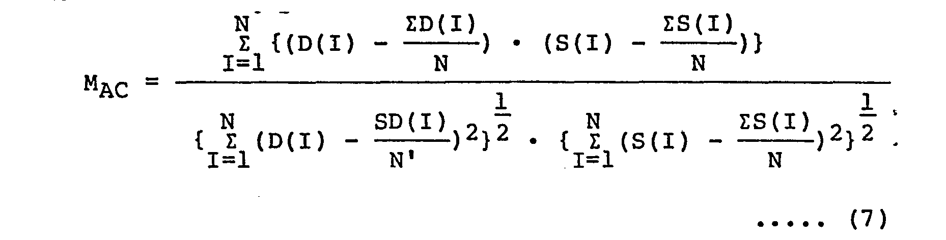
- While the alternating current component of the standard pattern signal S(I) can be calculated in advance, the detected pattern signal D(I) cannot be obtained unless the current note is scanned by the line sensor, that is, the alternating current component of the signal D(I) can be obtained only after the end of the scanning. By re-arranging the equation (7), we obtain

- Since the sum of the alternating current components S'(I) of the signal S(I) is zero,


- Fig. 13 shows the circuit of a currency not identification system which is based upon the principles discussed above. Basically, the circuit of Fig. 13 is the same as the embodiment of Fig. 9, and like parts are designated by like reference numerals. In this embodiment, the
line sensor 14 provides a scanning signal V(i) [i = 1 to 512] including 512 picture element signals corresponding to respective picture elements for every scanning. The scanning signal V(i) is coupled through theamplifier 15 to the A/D converter 41, which converts the individual component picture element signals at levels corresponding to the intensity of light incident on the picture elements of the line sensor into corresponding 8-bit digital picture element signals. These 512 digital picture element signals are inputted to theadder 42 and the signal detectionarea determination circuit 45. The average value of these picutre element signals is calculated by theadder 12. The digital signal D(i) presenting the average value, obtained from theadder 42, is supplied todata switch 43 anddata selector 44. The data switch 43 is switched in response to the timing pulse T2 to transfer the output signal D(i) of theadder 42 to thebuffer memory 47 or transfer the data D(i) stored in thebuffer memory 47 to thedata selector 44.The'data selector 44 selects the signal Dl(i) and supplies it to thelatch circuit 48. for a first period TF and selects the signal D2(i) read . out from thebuffer memory 47 and supplied to thelatch circuit 48 for a second period TB in response to the timing pulse T4. Thelatch circuit 48 provides N/2 sampled data DF(J) for the 50 points from the start point Qg for the first period TF and N/2 sampled data DB(L) for the 50 points from the end point QE in response to the timing pulse T5. Thelatch circuit 48 supplies the signals DF(I) and DB(I) in response to the timing pulse T5. Thedata selector 54 selects signal DF(I), signal DSF (I, K) and decimal signal "1" and supplies a signal D5(I) under the control of the timing pulse T6. As the signal DSF(I, K) are provided K different standard pattern data (calculated according to the equation (10)) stored in thestandard pattern memory 55. Themultiplier 52 first calculates the product of DF(I) and DF(I), i.e., DF(I)2, then DF(I) and then the product of DF(I) and DSF(I, K), i.e., DF(I)·DSF(I, K). It provides the result as a signal D7, which is processed through theadder 56,latch circuit 57,data selector 58,latch circuits buffer memory 61 to obtain the product sum of the signal D7. Then signals QF, DF and RF(K) are calculated according to equations


microcomputor 51, which calculates the similarity MF(K) from the afore mentioned signals QF, DF and RF(K) according to an equation
- The sampled data DF(I) is used when producing the standard pattern data DSF(I, K).
- The similarity MF(K) obtained in the above way is that with respect to a predetermined area from the leading edge of the printed section of the currency note, and the similarity with respect to a predetermined area from the trailing edge is obtained similar to MF(K). In this case, the data DB(I) and DSB are used in the calculation.
- From MF(K) and MB(K) calculated in the above way, the overall similarity M(K) is calculated from the ((MF(K) + MS(K))/2 to detect the standard pattern data for which M(K) is maximum, and the kind of the currency note examined is determined from this standard pattern data. If M(K) is less than a limit value, for instance 0.6, the examined currency note is rejected as it corresponds to one of the currency notes represented by the standard pattern data.
- As has been described in the foregoing, with the currency note identification system according to the invention, the characteristic of a portion of a scanning signal obtained by scanning a printed matter, particularly a currency note, being examined is detected, the characteristic of a predetermined portion of the scanning signal of the currency note from the point corresponding to the afore mentioned detected portion of the scanning signal is detected, the similarity of the characteristic of the detected scanning signal is compared to that of a standard scanning signal, and the kind and/or genuineness of the examined currency note is determined from the calculated similarity, so that it is possible to obtain high performance identification as to the kind and/or genuineness of the currency note without substantially being affected by contaminations, shrinkage, wrinkles creases, etc.
- While in tha above embodiments the identification information is detected from the leading or trailing edge of the printed section of the currency note as the start point, it is also possible to detect the identification information from a pariticular point within the printed section as the start point. Further, according to the invention it is possible to identify not only currency notes but also other printed matter requiring identification such as securities. Further, while a line sensor has been used as means for providing the scanning signal, it is also possible to use a two-dimensional scanning device such as a video camera as well.
Claims (17)
Priority Applications (3)
| Application Number | Priority Date | Filing Date | Title |
|---|---|---|---|
| AT81104817T ATE18953T1 (en) | 1981-06-22 | 1981-06-22 | METHOD OF IDENTIFICATION OF BANKNOTES. |
| DE8181104817T DE3174234D1 (en) | 1981-06-22 | 1981-06-22 | System for identifying currency note |
| EP81104817A EP0067898B1 (en) | 1981-06-22 | 1981-06-22 | System for identifying currency note |
Applications Claiming Priority (1)
| Application Number | Priority Date | Filing Date | Title |
|---|---|---|---|
| EP81104817A EP0067898B1 (en) | 1981-06-22 | 1981-06-22 | System for identifying currency note |
Publications (2)
| Publication Number | Publication Date |
|---|---|
| EP0067898A1 true EP0067898A1 (en) | 1982-12-29 |
| EP0067898B1 EP0067898B1 (en) | 1986-04-02 |
Family
ID=8187781
Family Applications (1)
| Application Number | Title | Priority Date | Filing Date |
|---|---|---|---|
| EP81104817A Expired EP0067898B1 (en) | 1981-06-22 | 1981-06-22 | System for identifying currency note |
Country Status (3)
| Country | Link |
|---|---|
| EP (1) | EP0067898B1 (en) |
| AT (1) | ATE18953T1 (en) |
| DE (1) | DE3174234D1 (en) |
Cited By (7)
| Publication number | Priority date | Publication date | Assignee | Title |
|---|---|---|---|---|
| GB2190743A (en) * | 1986-05-19 | 1987-11-25 | Marconi Instruments Ltd | Compensating for misalignment in the comparison of patterns |
| EP0529746A2 (en) * | 1988-05-13 | 1993-03-03 | Canon Kabushiki Kaisha | Image processing apparatus |
| US5321470A (en) * | 1988-05-13 | 1994-06-14 | Canon Kabushiki Kaisha | Apparatus with anti-forgery provision |
| US5503262A (en) * | 1992-03-10 | 1996-04-02 | Mars Incorporated | Apparatus for the classification of a pattern for example on a banknote or a coin |
| WO1997026625A1 (en) * | 1996-01-16 | 1997-07-24 | Mars, Incorporated | Edge sensing |
| EP0802510A2 (en) * | 1996-04-15 | 1997-10-22 | Glory Kogyo Kabushiki Kaisha | Method of discriminating paper notes |
| AT508977B1 (en) * | 2009-10-28 | 2011-07-15 | Ait Austrian Inst Technology | BANKNOTE RECOGNITION WITH PROJECTION PROFILE |
Families Citing this family (13)
| Publication number | Priority date | Publication date | Assignee | Title |
|---|---|---|---|---|
| WO2018075838A1 (en) | 2016-10-21 | 2018-04-26 | The Procter & Gamble Company | Concentrated shampoo dosage of foam for providing hair care benefits |
| US11141361B2 (en) | 2016-10-21 | 2021-10-12 | The Procter And Gamble Plaza | Concentrated shampoo dosage of foam designating hair volume benefits |
| CN109843258A (en) | 2016-10-21 | 2019-06-04 | 宝洁公司 | Indicate the concentrated type shampoo foam of hair conditioning benefit |
| US11141370B2 (en) | 2017-06-06 | 2021-10-12 | The Procter And Gamble Company | Hair compositions comprising a cationic polymer mixture and providing improved in-use wet feel |
| US11224567B2 (en) | 2017-06-06 | 2022-01-18 | The Procter And Gamble Company | Hair compositions comprising a cationic polymer/silicone mixture providing improved in-use wet feel |
| MX2020003318A (en) | 2017-10-10 | 2021-12-06 | Procter & Gamble | Compact shampoo composition with amino acid based anionic surfactants and cationic polymers. |
| MX2020003316A (en) | 2017-10-10 | 2021-12-06 | Procter & Gamble | Compact shampoo composition containing sulfate-free surfactants. |
| JP2020536885A (en) | 2017-10-10 | 2020-12-17 | ザ プロクター アンド ギャンブル カンパニーThe Procter & Gamble Company | Sulfate-free personal cleansing composition with low mineral salt content |
| CN111201010A (en) | 2017-10-10 | 2020-05-26 | 宝洁公司 | Method of treating hair or skin with a personal care composition in the form of a foam |
| CN112367963A (en) | 2018-06-29 | 2021-02-12 | 宝洁公司 | Low surfactant aerosol anti-dandruff compositions |
| WO2021173203A1 (en) | 2020-02-27 | 2021-09-02 | The Procter & Gamble Company | Anti-dandruff compositions with sulfur having enhanced efficacy and aesthetics |
| US11819474B2 (en) | 2020-12-04 | 2023-11-21 | The Procter & Gamble Company | Hair care compositions comprising malodor reduction materials |
| US20220378684A1 (en) | 2021-05-14 | 2022-12-01 | The Procter & Gamble Company | Shampoo Compositions Containing a Sulfate-Free Surfactant System and Sclerotium Gum Thickener |
Citations (15)
| Publication number | Priority date | Publication date | Assignee | Title |
|---|---|---|---|---|
| US3781553A (en) * | 1972-11-28 | 1973-12-25 | B Podlaskin | Apparatus for analyzing an image |
| FR2196494A1 (en) * | 1972-07-28 | 1974-03-15 | Titn | |
| US4041456A (en) * | 1976-07-30 | 1977-08-09 | Ott David M | Method for verifying the denomination of currency |
| FR2349863A1 (en) * | 1976-04-30 | 1977-11-25 | Gretag Ag | PROCESS FOR ASSESSING THE PRINT QUALITY OF A DOCUMENT |
| US4131879A (en) * | 1976-04-30 | 1978-12-26 | Gretag Aktiengesellschaft | Method and apparatus for determining the relative positions of corresponding points or zones of a sample and an orginal |
| US4143279A (en) * | 1976-04-30 | 1979-03-06 | Gretag Aktiengesellschaft | Method and apparatus for testing the print quality of printed texts, more particularly banknotes |
| US4156231A (en) * | 1977-07-18 | 1979-05-22 | Fuji Electric Co. Ltd. | Automated pattern inspection system |
| US4179685A (en) * | 1976-11-08 | 1979-12-18 | Abbott Coin Counter Company, Inc. | Automatic currency identification system |
| EP0012723A1 (en) * | 1978-12-18 | 1980-06-25 | GRETAG Aktiengesellschaft | Process for mechanically assessing the print quality of a printed product and device for performing the same |
| US4255652A (en) * | 1979-01-31 | 1981-03-10 | Coulter Systems Corporation | High speed electrically responsive indicia detecting apparatus and method |
| US4255057A (en) * | 1979-10-04 | 1981-03-10 | The Perkin-Elmer Corporation | Method for determining quality of U.S. currency |
| WO1981001211A1 (en) * | 1979-10-16 | 1981-04-30 | Ardac Inc | Security validator |
| DE2945651A1 (en) * | 1979-11-12 | 1981-05-21 | Tokyo Shibaura Denki K.K., Kawasaki, Kanagawa | Sheet e.g. banknote authenticity tester - measures check parameters opto-electrically under object position-dependent evaluation control |
| DE3040963A1 (en) * | 1979-10-31 | 1981-05-21 | Tokyo Shibaura Denki K.K., Kawasaki, Kanagawa | BANKNOTE IDENTIFICATION SYSTEM |
| GB2064111A (en) * | 1979-11-22 | 1981-06-10 | Tokyo Shibaura Electric Co | Discriminating sheets |
Family Cites Families (3)
| Publication number | Priority date | Publication date | Assignee | Title |
|---|---|---|---|---|
| IT1068657B (en) * | 1976-11-03 | 1985-03-21 | Nuovo Pignone Spa | PERFECTED METHOD FOR CHECKING BANKNOTES AND EQUIPMENT TO MAKE IT |
| DE2809707A1 (en) * | 1978-03-07 | 1979-10-11 | Messerschmitt Boelkow Blohm | Monitoring and recording system for handling currency notes - uses search store for checking of notes and signal unit controlling working store |
| US4311914A (en) * | 1978-12-18 | 1982-01-19 | Gretag Aktiengesellschaft | Process for assessing the quality of a printed product |
-
1981
- 1981-06-22 DE DE8181104817T patent/DE3174234D1/en not_active Expired
- 1981-06-22 AT AT81104817T patent/ATE18953T1/en not_active IP Right Cessation
- 1981-06-22 EP EP81104817A patent/EP0067898B1/en not_active Expired
Patent Citations (16)
| Publication number | Priority date | Publication date | Assignee | Title |
|---|---|---|---|---|
| FR2196494A1 (en) * | 1972-07-28 | 1974-03-15 | Titn | |
| US3781553A (en) * | 1972-11-28 | 1973-12-25 | B Podlaskin | Apparatus for analyzing an image |
| FR2349863A1 (en) * | 1976-04-30 | 1977-11-25 | Gretag Ag | PROCESS FOR ASSESSING THE PRINT QUALITY OF A DOCUMENT |
| US4131879A (en) * | 1976-04-30 | 1978-12-26 | Gretag Aktiengesellschaft | Method and apparatus for determining the relative positions of corresponding points or zones of a sample and an orginal |
| US4143279A (en) * | 1976-04-30 | 1979-03-06 | Gretag Aktiengesellschaft | Method and apparatus for testing the print quality of printed texts, more particularly banknotes |
| US4041456A (en) * | 1976-07-30 | 1977-08-09 | Ott David M | Method for verifying the denomination of currency |
| US4179685A (en) * | 1976-11-08 | 1979-12-18 | Abbott Coin Counter Company, Inc. | Automatic currency identification system |
| US4156231A (en) * | 1977-07-18 | 1979-05-22 | Fuji Electric Co. Ltd. | Automated pattern inspection system |
| EP0012723A1 (en) * | 1978-12-18 | 1980-06-25 | GRETAG Aktiengesellschaft | Process for mechanically assessing the print quality of a printed product and device for performing the same |
| US4255652A (en) * | 1979-01-31 | 1981-03-10 | Coulter Systems Corporation | High speed electrically responsive indicia detecting apparatus and method |
| US4255057A (en) * | 1979-10-04 | 1981-03-10 | The Perkin-Elmer Corporation | Method for determining quality of U.S. currency |
| WO1981001211A1 (en) * | 1979-10-16 | 1981-04-30 | Ardac Inc | Security validator |
| EP0028089A2 (en) * | 1979-10-16 | 1981-05-06 | Ardac, Inc. | Security validator |
| DE3040963A1 (en) * | 1979-10-31 | 1981-05-21 | Tokyo Shibaura Denki K.K., Kawasaki, Kanagawa | BANKNOTE IDENTIFICATION SYSTEM |
| DE2945651A1 (en) * | 1979-11-12 | 1981-05-21 | Tokyo Shibaura Denki K.K., Kawasaki, Kanagawa | Sheet e.g. banknote authenticity tester - measures check parameters opto-electrically under object position-dependent evaluation control |
| GB2064111A (en) * | 1979-11-22 | 1981-06-10 | Tokyo Shibaura Electric Co | Discriminating sheets |
Non-Patent Citations (2)
| Title |
|---|
| Microelectronics Journal, Vol. 10, No. 1 (1979) Mackingtosh Publications Ltd. Luton, GB C. TASSEL et al.: "Photodiode Arrays-Characteristics and Applications", pages 35-43 * page 41, 7.3 "Bank Note Inspection", 8 "Array Scanning", page 42, 9. "Applications of the Two-Dimensional Array" figure 12; page 43, 10. "Conclusion" * * |
| Proceedings 1979 Carnahan Conference on Crime Countermeasures, May 16-18, 1979 University of Kentucky, Lexington, Kentucky, US W. SZEPANSKI: "A Signal Theoretic Method for Creating Forgery-Proof Documents for Automatic Verification" pages 101-109 * the whole document * * |
Cited By (18)
| Publication number | Priority date | Publication date | Assignee | Title |
|---|---|---|---|---|
| GB2190743A (en) * | 1986-05-19 | 1987-11-25 | Marconi Instruments Ltd | Compensating for misalignment in the comparison of patterns |
| GB2190743B (en) * | 1986-05-19 | 1990-02-07 | Marconi Instruments Ltd | Pattern alignment generator |
| US5765089A (en) * | 1988-05-13 | 1998-06-09 | Canon Kabushiki Kaisha | Image processing apparatus and method for generating a control signal based on a discrimination of whether an input image includes a specific image |
| US5583614A (en) * | 1988-05-13 | 1996-12-10 | Canon Kabushiki Kaisha | Image processing apparatus and method for determining whether an original contains a specified image |
| EP0529745A3 (en) * | 1988-05-13 | 1993-05-05 | Canon Kabushiki Kaisha | Image processing apparatus |
| EP0529746A3 (en) * | 1988-05-13 | 1993-05-05 | Canon Kabushiki Kaisha | Image processing apparatus |
| US5321470A (en) * | 1988-05-13 | 1994-06-14 | Canon Kabushiki Kaisha | Apparatus with anti-forgery provision |
| US6185404B1 (en) | 1988-05-13 | 2001-02-06 | Canon Kabushiki Kaisha | Image processing apparatus and method for generating a control signal based on a discrimination of whether an input image includes a specific image |
| EP0529746A2 (en) * | 1988-05-13 | 1993-03-03 | Canon Kabushiki Kaisha | Image processing apparatus |
| EP0529745A2 (en) * | 1988-05-13 | 1993-03-03 | Canon Kabushiki Kaisha | Image processing apparatus |
| US5522491A (en) * | 1992-03-10 | 1996-06-04 | Mars Incorporated | Method for the classification of a pattern, for example on a banknote or a coin |
| US5503262A (en) * | 1992-03-10 | 1996-04-02 | Mars Incorporated | Apparatus for the classification of a pattern for example on a banknote or a coin |
| WO1997026625A1 (en) * | 1996-01-16 | 1997-07-24 | Mars, Incorporated | Edge sensing |
| US6188080B1 (en) | 1996-01-16 | 2001-02-13 | Mars Incorporated | Apparatus for determining the location of an edge of a document |
| US6359287B1 (en) | 1996-01-16 | 2002-03-19 | Mars Incorporated | Apparatus for detecting an edge of a document |
| EP0802510A2 (en) * | 1996-04-15 | 1997-10-22 | Glory Kogyo Kabushiki Kaisha | Method of discriminating paper notes |
| EP0802510A3 (en) * | 1996-04-15 | 1999-02-03 | Glory Kogyo Kabushiki Kaisha | Method of discriminating paper notes |
| AT508977B1 (en) * | 2009-10-28 | 2011-07-15 | Ait Austrian Inst Technology | BANKNOTE RECOGNITION WITH PROJECTION PROFILE |
Also Published As
| Publication number | Publication date |
|---|---|
| EP0067898B1 (en) | 1986-04-02 |
| DE3174234D1 (en) | 1986-05-07 |
| ATE18953T1 (en) | 1986-04-15 |
Similar Documents
| Publication | Publication Date | Title |
|---|---|---|
| US4464786A (en) | System for identifying currency note | |
| EP0067898B1 (en) | System for identifying currency note | |
| EP0069893B1 (en) | A printed matter identifying apparatus and method | |
| US4910787A (en) | Discriminator between handwritten and machine-printed characters | |
| EP0078708B1 (en) | Apparatus for sorting sheets according to their patterns | |
| EP0294497B1 (en) | Apparatus for identifying postage stamps | |
| US4601057A (en) | Pattern analyzer | |
| GB2062854A (en) | Currency note idenification system | |
| CA2109791A1 (en) | Method and apparatus for currency discrimination and counting | |
| US5020110A (en) | Arrangement for checking documents | |
| JPH06274736A (en) | Coin recognition device | |
| EP0858048B1 (en) | Apparatus of optically reading character and method thereof | |
| EP0859343A2 (en) | Method and apparatus for screening documents | |
| KR100194748B1 (en) | Banknotes Identification Device | |
| JP2002092683A (en) | Device for discriminating between true and false medium | |
| CA1178711A (en) | Apparatus and process for scanning and analyzing mail address information | |
| JPH10198837A (en) | Paper sheet discriminating device | |
| JP2511508B2 (en) | Paper discrimination device | |
| JPH10302110A (en) | Paper money discrimination device | |
| JP2647238B2 (en) | Bill validator | |
| JPS6367225B2 (en) | ||
| JPS59160284A (en) | Discriminator for printed matter | |
| KR100200220B1 (en) | Bank-note discrimination | |
| JPS584494A (en) | Printed matter discriminator | |
| JP4306027B2 (en) | Paper sheet authenticity discrimination device |
Legal Events
| Date | Code | Title | Description |
|---|---|---|---|
| PUAI | Public reference made under article 153(3) epc to a published international application that has entered the european phase |
Free format text: ORIGINAL CODE: 0009012 |
|
| 17P | Request for examination filed |
Effective date: 19810623 |
|
| AK | Designated contracting states |
Designated state(s): AT CH DE FR GB IT LI SE |
|
| RAP1 | Party data changed (applicant data changed or rights of an application transferred) |
Owner name: KABUSHIKI KAISHA TOSHIBA |
|
| RBV | Designated contracting states (corrected) |
Designated state(s): AT DE GB IT |
|
| GRAA | (expected) grant |
Free format text: ORIGINAL CODE: 0009210 |
|
| ITF | It: translation for a ep patent filed |
Owner name: BUGNION S.P.A. |
|
| AK | Designated contracting states |
Kind code of ref document: B1 Designated state(s): AT DE GB IT |
|
| REF | Corresponds to: |
Ref document number: 18953 Country of ref document: AT Date of ref document: 19860415 Kind code of ref document: T |
|
| REF | Corresponds to: |
Ref document number: 3174234 Country of ref document: DE Date of ref document: 19860507 |
|
| PLBI | Opposition filed |
Free format text: ORIGINAL CODE: 0009260 |
|
| 26 | Opposition filed |
Opponent name: GAO GESELLSCHAFT FUER AUTOMATION UND ORGANISATION Effective date: 19861223 |
|
| ITTA | It: last paid annual fee | ||
| PGFP | Annual fee paid to national office [announced via postgrant information from national office to epo] |
Ref country code: AT Payment date: 19940614 Year of fee payment: 14 |
|
| PGFP | Annual fee paid to national office [announced via postgrant information from national office to epo] |
Ref country code: GB Payment date: 19940615 Year of fee payment: 14 |
|
| PGFP | Annual fee paid to national office [announced via postgrant information from national office to epo] |
Ref country code: DE Payment date: 19940622 Year of fee payment: 14 |
|
| RDAG | Patent revoked |
Free format text: ORIGINAL CODE: 0009271 |
|
| STAA | Information on the status of an ep patent application or granted ep patent |
Free format text: STATUS: PATENT REVOKED |
|
| 27W | Patent revoked |
Effective date: 19950131 |
|
| GBPR | Gb: patent revoked under art. 102 of the ep convention designating the uk as contracting state |
Free format text: 950131 |
|
| APAH | Appeal reference modified |
Free format text: ORIGINAL CODE: EPIDOSCREFNO |