EP0068123A2 - Synchronization apparatus - Google Patents
Synchronization apparatus Download PDFInfo
- Publication number
- EP0068123A2 EP0068123A2 EP82104114A EP82104114A EP0068123A2 EP 0068123 A2 EP0068123 A2 EP 0068123A2 EP 82104114 A EP82104114 A EP 82104114A EP 82104114 A EP82104114 A EP 82104114A EP 0068123 A2 EP0068123 A2 EP 0068123A2
- Authority
- EP
- European Patent Office
- Prior art keywords
- controller
- controller units
- accordance
- input
- output
- Prior art date
- Legal status (The legal status is an assumption and is not a legal conclusion. Google has not performed a legal analysis and makes no representation as to the accuracy of the status listed.)
- Granted
Links
Images

Classifications
-
- G—PHYSICS
- G09—EDUCATION; CRYPTOGRAPHY; DISPLAY; ADVERTISING; SEALS
- G09G—ARRANGEMENTS OR CIRCUITS FOR CONTROL OF INDICATING DEVICES USING STATIC MEANS TO PRESENT VARIABLE INFORMATION
- G09G5/00—Control arrangements or circuits for visual indicators common to cathode-ray tube indicators and other visual indicators
- G09G5/12—Synchronisation between the display unit and other units, e.g. other display units, video-disc players
Definitions
- This invention relates to control circuits for input/output devices and relates more particularly to circuits for maintaining synchronization between two or more controllers of input/output devices.
- I/O input/output
- CRT cathode ray tube
- U.S. patent 3,996,584 shows a display which can be fed by two character generators, such that foreign languages can be displayed. This system operates by including a character generator control which selects one or the other of the two character generators, and this is distinguished since both do not operate simultaneously.
- U.S. patent 4,020,472 shows a plurality of controllers which respond to signals from a single processor, and control individual I/O units. However, in this reference no synchronization between the two controllers is necessary since they feed different display units.
- one or more auxiliary or slave CRT controllers connected to a common CRT are synchronized to a master controller so that they remain in synchronism so long as they are programmed with the same screen refresh parameters. This is accomplished by generating a synchronizing signal and then allowing the unsynchronized slave controller or controllers to run until they reach their vertical retrace time, at which time the character clock for the auxiliary or slave controller is stopped, thereby freezing the slave controllers in that state. When the master clock reaches its vertical retrace time, the character clock to the slave controllers is restarted and the master and slave controllers thereafter run in synchronism.
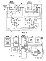
- the synchronizing circuitry of the present invention is shown in the dotted enclosure 10 in FIG. 1 in connection with a pair of CRT controllers 11, 12 which control a single CRT (not shown).
- Controllers 11, 12 may be of any suitable type, such as chip CRT controllers manufactured by Intel Corporation under the designation of Type 8275.
- Controller 11 is designated as the master and controller 12 is identified as the slave controller.
- a synchronizing command signal to perform synchronization of the two controllers in accordance with the present invention may be generated by a central processing unit (CPU) and appears on a line 13 as the "clear" input to a flip-flop 14.
- CPU central processing unit
- controllers 11, 12 Prior to receipt of this sync pulse, controllers 11, 12 may be operating in an unsynchronized mode under control of a character clock input on terminal 16. With sync line 13 having a zero, and flip-flop 14 therefore having a zero on its "clear” input, output Q of flip-flop 14 is zero and output Q is one. The Q output of flip-flop 14 is also supplied to the "clear" input of a flip-flop 23, causing the Q output of this flip-flop which is supplied as the other input to OR gate 17 to become zero. The output from Q of flip-flop 14 passes through OR gate 17 and is supplied as an input to an AND gate 18. The other input to gate 18 is a character clock signal from terminal 16. Under these conditions, the clock signals pass through gate 18 to the CCLK input of controller 12.
- FIG. 2 illustrates an application of the synchronizing circuitry 10 of the present invention to two CRT controllers which share control of the characters and color on a single CRT.
- the character information is supplied in the character buffer section of a memory 31 and the corresponding color attribute information for each character is stored in the color buffer section of memory 31.
- the character information from memory 31 is supplied through a direct memory access device (DMA) 32 to master controller 11.
- DMA direct memory access device
- the 7 bit output of master controller 11 is supplied as character address information to a character generator circuit 33.
- the output of generator 33 is fed through a shift register 34 to form the character video signal to a character and color defining circuit 36.
- the color information from memory 31 is supplied through DMA 32 to the input of slave controller 12.
- Three of the output lines of slave controller 12 convey information relative to character background color and three other output lines convey informtion relative to character foreground color.
- the six lines are supplied to circuitry 36 which performs a six-to-three select operation to produce appropriate signals on its red, green and blue output lines. This information, together with the vertical and horizontal retrace signals, are sent to the color CRT (not shown).
- One feature of the embodiment of FIG. 2 is that the seventh bit in the output of slave controller 12, which is not required for color definition, can be supplied as shown to master controller 11. This results in the availability of 8 bits in controller 11 for character addressing, thus supporting character code sizes greater than seven bits, such as EBCDIC.
- synchronization control circuitry 10 operates as described above in connection with FIG. 1 to produce synchronization of controllers 11 and 12 when the sync line is raised by the CPU.
- FIG. 3 illustrates another application of the present invention in connection with attribute information relative to displayed characters.
- memory 31 again holds character information which is supplied through DMA 32 to master controller 11.
- the seven output bits are supplied as character address information to character generator 33 whose output is supplied through shift register 34 to form the character video input signal which is supplied to character attribute circuitry 37.
- Another section of memory 31 contains attribute information about each character and this information is supplied through DMA 32 to slave controller 12.
- the attributes are assumed to be reverse video, blink, underline and highlight.
- four of the output lines from slave controller 12 are supplied to circuitry 37 with this attribute information for each character.
- the output from circuitry 37 is supplied as the video signal to a CRT (not shown), along with the vertical and horizontal retrace signals.
- controller 12 which are not used to convey attribute information are supplied as inputs to character generator 33, thereby resulting in the availability of ten bits for character addressing.
- the synchronization control circuitry 10 operates to synchronize slave controller 12 with master controller 11 when the CPU raises the sync line.
- FIG. 4 illustrates another application of the present invention which allows more than one CPU to display data on a single CRT.
- Two CPU's 41, 42 are shown, although a larger number may be employed, provided the appropriate number of controllers are used.
- CPU 41 supplies information to the character buffer portion of memory 31 which is sent to master controller 11 through DMA 32.
- the output of controller 11 is supplied as before to character generator 33 whose output is supplied through shift register 34 to attribute control circuitry (ATR) 43.
- ATR attribute control circuitry
- the output of this circuitry is supplied as the video signal to an OR gate 44 whose output is sent to the CRT (not shown).
- CPU 42 controls the character buffer section of memory 31' to send character information through DMA 32' to slave controller 12.
- the output of slave controller 12 is sent through character generator 33' to shift register 34' whose output is supplied to ATR control circuitry 43'.
- the video output signal is sent as another input to OR gate 44.
- An embodiment similar to that shown in FIG. 4 allows up to N processors to display data on a single CRT screen. This can be used for split screen multi-work stations or to permit two or more processors in a control application to display information to an operator on a single CRT screen.
- Another attribute of this invention is that additional controllers can be added with no additional logic on the base controller design. This allows the additional controllers to be added very easily as incremental features without increasing the cost of the base design.
Abstract
Description
- This invention relates to control circuits for input/output devices and relates more particularly to circuits for maintaining synchronization between two or more controllers of input/output devices.
- It may be desirable in the control of an input/output (I/O) device, such as a cathode ray tube (CRT) display, to provide more control function than is available from a single commercially available CRT controller chip. In this situation, one or more additional CRT controller chips can be employed to provide the additional control function, provided that the controller chips are properly synchronized with each other.
- U.S. patent 3,996,584 shows a display which can be fed by two character generators, such that foreign languages can be displayed. This system operates by including a character generator control which selects one or the other of the two character generators, and this is distinguished since both do not operate simultaneously.
- U.S. patent 4,020,472 shows a plurality of controllers which respond to signals from a single processor, and control individual I/O units. However, in this reference no synchronization between the two controllers is necessary since they feed different display units.
- In accordance with the present invention, one or more auxiliary or slave CRT controllers connected to a common CRT are synchronized to a master controller so that they remain in synchronism so long as they are programmed with the same screen refresh parameters. This is accomplished by generating a synchronizing signal and then allowing the unsynchronized slave controller or controllers to run until they reach their vertical retrace time, at which time the character clock for the auxiliary or slave controller is stopped, thereby freezing the slave controllers in that state. When the master clock reaches its vertical retrace time, the character clock to the slave controllers is restarted and the master and slave controllers thereafter run in synchronism.
-
- FIG. 1 is a diagram showing synchronizing circuitry for carrying out the present invention; and
- FIGs. 2-4 show different applications of the synchronizing circuitry of FIG. 1 to the control of a single CRT.
- The synchronizing circuitry of the present invention is shown in the
dotted enclosure 10 in FIG. 1 in connection with a pair ofCRT controllers Controllers Controller 11 is designated as the master andcontroller 12 is identified as the slave controller. A synchronizing command signal to perform synchronization of the two controllers in accordance with the present invention may be generated by a central processing unit (CPU) and appears on a line 13 as the "clear" input to a flip-flop 14. - Prior to receipt of this sync pulse,
controllers terminal 16. With sync line 13 having a zero, and flip-flop 14 therefore having a zero on its "clear" input, output Q of flip-flop 14 is zero and output Q is one. The Q output of flip-flop 14 is also supplied to the "clear" input of a flip-flop 23, causing the Q output of this flip-flop which is supplied as the other input toOR gate 17 to become zero. The output from Q of flip-flop 14 passes through ORgate 17 and is supplied as an input to anAND gate 18. The other input togate 18 is a character clock signal fromterminal 16. Under these conditions, the clock signals pass throughgate 18 to the CCLK input ofcontroller 12. - When the sync signal goes to a one on line 13, this removes the "clear" on flip-
flop 14.Slave controller 12 continues to run until time for its vertical retrace, at which time the output line VRTC incontroller 12 is raised and supplied through a flip-flop 21 which acts to synchronize the pulse to the character clock. This causes the Q output of flip-flop 21 to become a one, which is supplied as a clock input to flip-flop 14, causing flip-flop 14 to change state so that Q is a one and Q is a zero. Hence, under these conditions, there are no inputs to ORgate 17. This removes an enabling input fromgate 18 which had been provided through ORgate 17, so that the character clock pulses can no longer pass throughgate 18 to controller 12. - At this point the
slave controller 12 is effectively frozen in that state with its character clock stopped. Also, at this time the Q output of flip-flop 14 is supplied to remove the "clear" input of flip-flop 23. - When
master controller 11 reaches its vertical retrace time, its output line VRTC rises and is transmitted through synchronizing flip-flop 22 to the clock input of flip-flop 23. This causes the Q output of flip-flop 23 to become a one and this output is passed through ORgate 17 togate 18, thereby allowing the character clock pulses throughgate 18 toslave controller 12.Controllers - A summary of the status of the different flip-flops during the operation is shown in the table below.

- FIG. 2 illustrates an application of the synchronizing
circuitry 10 of the present invention to two CRT controllers which share control of the characters and color on a single CRT. The character information is supplied in the character buffer section of amemory 31 and the corresponding color attribute information for each character is stored in the color buffer section ofmemory 31. The character information frommemory 31 is supplied through a direct memory access device (DMA) 32 tomaster controller 11. The 7 bit output ofmaster controller 11 is supplied as character address information to acharacter generator circuit 33. The output ofgenerator 33 is fed through ashift register 34 to form the character video signal to a character andcolor defining circuit 36. - The color information from
memory 31 is supplied throughDMA 32 to the input ofslave controller 12. Three of the output lines ofslave controller 12 convey information relative to character background color and three other output lines convey informtion relative to character foreground color. The six lines are supplied tocircuitry 36 which performs a six-to-three select operation to produce appropriate signals on its red, green and blue output lines. This information, together with the vertical and horizontal retrace signals, are sent to the color CRT (not shown). - One feature of the embodiment of FIG. 2 is that the seventh bit in the output of
slave controller 12, which is not required for color definition, can be supplied as shown to mastercontroller 11. This results in the availability of 8 bits incontroller 11 for character addressing, thus supporting character code sizes greater than seven bits, such as EBCDIC. - It will be understood that in the embodiment of FIG. 2,
synchronization control circuitry 10 operates as described above in connection with FIG. 1 to produce synchronization ofcontrollers - FIG. 3 illustrates another application of the present invention in connection with attribute information relative to displayed characters. In FIG. 3,
memory 31 again holds character information which is supplied throughDMA 32 tomaster controller 11. As before, the seven output bits are supplied as character address information tocharacter generator 33 whose output is supplied throughshift register 34 to form the character video input signal which is supplied tocharacter attribute circuitry 37. - Another section of
memory 31 contains attribute information about each character and this information is supplied throughDMA 32 toslave controller 12. In the example illustrated, the attributes are assumed to be reverse video, blink, underline and highlight. Hence, four of the output lines fromslave controller 12 are supplied tocircuitry 37 with this attribute information for each character. The output fromcircuitry 37 is supplied as the video signal to a CRT (not shown), along with the vertical and horizontal retrace signals. - The output bits of
controller 12 which are not used to convey attribute information are supplied as inputs tocharacter generator 33, thereby resulting in the availability of ten bits for character addressing. As in the embodiment of FIG. 2, thesynchronization control circuitry 10 operates to synchronizeslave controller 12 withmaster controller 11 when the CPU raises the sync line. - FIG. 4 illustrates another application of the present invention which allows more than one CPU to display data on a single CRT. Two CPU's 41, 42, are shown, although a larger number may be employed, provided the appropriate number of controllers are used.
CPU 41 supplies information to the character buffer portion ofmemory 31 which is sent tomaster controller 11 throughDMA 32. The output ofcontroller 11 is supplied as before tocharacter generator 33 whose output is supplied throughshift register 34 to attribute control circuitry (ATR) 43. The output of this circuitry is supplied as the video signal to anOR gate 44 whose output is sent to the CRT (not shown). - CPU 42 controls the character buffer section of memory 31' to send character information through DMA 32' to
slave controller 12. The output ofslave controller 12 is sent through character generator 33' to shift register 34' whose output is supplied to ATR control circuitry 43'. The video output signal is sent as another input to ORgate 44. - An embodiment similar to that shown in FIG. 4 allows up to N processors to display data on a single CRT screen. This can be used for split screen multi-work stations or to permit two or more processors in a control application to display information to an operator on a single CRT screen.
- Another attribute of this invention is that additional controllers can be added with no additional logic on the base controller design. This allows the additional controllers to be added very easily as incremental features without increasing the cost of the base design.
Claims (8)
Applications Claiming Priority (2)
| Application Number | Priority Date | Filing Date | Title |
|---|---|---|---|
| US06/279,368 US4495594A (en) | 1981-07-01 | 1981-07-01 | Synchronization of CRT controller chips |
| US279368 | 1981-07-01 |
Publications (3)
| Publication Number | Publication Date |
|---|---|
| EP0068123A2 true EP0068123A2 (en) | 1983-01-05 |
| EP0068123A3 EP0068123A3 (en) | 1983-03-23 |
| EP0068123B1 EP0068123B1 (en) | 1985-09-04 |
Family
ID=23068658
Family Applications (1)
| Application Number | Title | Priority Date | Filing Date |
|---|---|---|---|
| EP82104114A Expired EP0068123B1 (en) | 1981-07-01 | 1982-05-12 | Synchronization apparatus |
Country Status (6)
| Country | Link |
|---|---|
| US (1) | US4495594A (en) |
| EP (1) | EP0068123B1 (en) |
| JP (1) | JPS589192A (en) |
| CA (1) | CA1172386A (en) |
| DE (1) | DE3265998D1 (en) |
| MY (1) | MY8800011A (en) |
Cited By (5)
| Publication number | Priority date | Publication date | Assignee | Title |
|---|---|---|---|---|
| US4467412A (en) * | 1981-05-18 | 1984-08-21 | Atari, Inc. | Slave processor with clock controlled by internal ROM & master processor |
| EP0247710A2 (en) * | 1986-05-30 | 1987-12-02 | International Computers Limited | Data display apparatus |
| WO1996003836A1 (en) * | 1994-07-25 | 1996-02-08 | Australian Research And Design Corporation Pty Ltd. | A controller for providing timing signals for video data |
| WO1998032068A1 (en) * | 1997-01-17 | 1998-07-23 | Intergraph Corporation | Multiple display synchronization apparatus and method |
| US11912467B2 (en) | 2021-02-05 | 2024-02-27 | Ica S.P.A. | Closing system for packages with closeable interlocking element |
Families Citing this family (17)
| Publication number | Priority date | Publication date | Assignee | Title |
|---|---|---|---|---|
| GB2123656B (en) * | 1982-06-09 | 1987-02-18 | Tatsumi Denshi Kogyo Kk | A method and an apparatus for displaying a unified picture on crt screens of multiple displaying devices |
| US4621319A (en) * | 1982-09-27 | 1986-11-04 | Intel Corporation | Personal development system |
| JPS60117376A (en) * | 1983-11-29 | 1985-06-24 | Yokogawa Medical Syst Ltd | Picture display device for computerized tomographic image pickup device |
| JPH0640256B2 (en) * | 1983-12-26 | 1994-05-25 | 株式会社日立製作所 | Display controller |
| FR2566951B1 (en) * | 1984-06-29 | 1986-12-26 | Texas Instruments France | METHOD AND SYSTEM FOR DISPLAYING VISUAL INFORMATION ON A SCREEN BY LINE-BY-LINE AND POINT-BY-POINT SCREEN OF VIDEO FRAMES |
| US4654804A (en) * | 1984-07-23 | 1987-03-31 | Texas Instruments Incorporated | Video system with XY addressing capabilities |
| US4660155A (en) * | 1984-07-23 | 1987-04-21 | Texas Instruments Incorported | Single chip video system with separate clocks for memory controller, CRT controller |
| JPS61194557A (en) * | 1985-02-25 | 1986-08-28 | Hitachi Ltd | Controlling lsi |
| US4683469A (en) * | 1985-03-14 | 1987-07-28 | Itt Corporation | Display terminal having multiple character display formats |
| US5265201A (en) * | 1989-11-01 | 1993-11-23 | Audio Precision, Inc. | Master-slave processor human interface system |
| US6157395A (en) * | 1997-05-19 | 2000-12-05 | Hewlett-Packard Company | Synchronization of frame buffer swapping in multi-pipeline computer graphics display systems |
| US6122000A (en) * | 1997-06-03 | 2000-09-19 | Hewlett Packard Company | Synchronization of left/right channel display and vertical refresh in multi-display stereoscopic computer graphics systems |
| FR2840753A1 (en) * | 2002-06-06 | 2003-12-12 | Artabel | Digital image computer assembly processing having video signals decoded producing pixel/clock synchronisation signal and pixel signals generated applying OR logic two pixel signals |
| WO2004045293A1 (en) * | 2002-11-18 | 2004-06-03 | Hydrodyne Incorporated | Improvement in shock wave tenderization of meat |
| US7256628B2 (en) * | 2003-01-29 | 2007-08-14 | Sun Microsystems, Inc. | Speed-matching control method and circuit |
| US20110043514A1 (en) * | 2009-08-24 | 2011-02-24 | ATI Technologies ULC. | Method and apparatus for multiple display synchronization |
| US8866825B2 (en) | 2010-12-15 | 2014-10-21 | Ati Technologies Ulc | Multiple display frame rendering method and apparatus |
Citations (1)
| Publication number | Priority date | Publication date | Assignee | Title |
|---|---|---|---|---|
| US3810119A (en) * | 1971-05-04 | 1974-05-07 | Us Navy | Processor synchronization scheme |
Family Cites Families (11)
| Publication number | Priority date | Publication date | Assignee | Title |
|---|---|---|---|---|
| US3996584A (en) * | 1973-04-16 | 1976-12-07 | Burroughs Corporation | Data handling system having a plurality of interrelated character generators |
| US3996585A (en) * | 1974-06-11 | 1976-12-07 | International Business Machines Corporation | Video generator circuit for a dynamic digital television display |
| US4020472A (en) * | 1974-10-30 | 1977-04-26 | Motorola, Inc. | Master slave registers for interface adaptor |
| US4079188A (en) * | 1975-04-14 | 1978-03-14 | Datotek, Inc. | Multi-mode digital enciphering system |
| US4197590A (en) * | 1976-01-19 | 1980-04-08 | Nugraphics, Inc. | Method for dynamically viewing image elements stored in a random access memory array |
| JPS603198B2 (en) * | 1976-08-23 | 1985-01-26 | 株式会社日立製作所 | Parallel synchronous timing generator |
| US4099236A (en) * | 1977-05-20 | 1978-07-04 | Intel Corporation | Slave microprocessor for operation with a master microprocessor and a direct memory access controller |
| US4183089A (en) * | 1977-08-30 | 1980-01-08 | Xerox Corporation | Data communications system for a reproduction machine having a master and secondary controllers |
| JPS602711B2 (en) * | 1979-03-08 | 1985-01-23 | ブラザー工業株式会社 | How to synchronize multiple microcomputers |
| US4393377A (en) * | 1980-08-12 | 1983-07-12 | Pitney Bowes Inc. | Circuit for controlling information on a display |
| US4386410A (en) * | 1981-02-23 | 1983-05-31 | Texas Instruments Incorporated | Display controller for multiple scrolling regions |
-
1981
- 1981-07-01 US US06/279,368 patent/US4495594A/en not_active Expired - Lifetime
-
1982
- 1982-05-12 DE DE8282104114T patent/DE3265998D1/en not_active Expired
- 1982-05-12 EP EP82104114A patent/EP0068123B1/en not_active Expired
- 1982-05-17 JP JP57081716A patent/JPS589192A/en active Granted
- 1982-05-21 CA CA000403583A patent/CA1172386A/en not_active Expired
-
1988
- 1988-12-30 MY MY11/88A patent/MY8800011A/en unknown
Patent Citations (1)
| Publication number | Priority date | Publication date | Assignee | Title |
|---|---|---|---|---|
| US3810119A (en) * | 1971-05-04 | 1974-05-07 | Us Navy | Processor synchronization scheme |
Non-Patent Citations (1)
| Title |
|---|
| IBM TECHNICAL DISCLOSURE BULLETIN, vol. 24, no. 4,September 1981 D.F. BANTZ et al.: "Multiple Display Processors", pages 1998-2000 * |
Cited By (7)
| Publication number | Priority date | Publication date | Assignee | Title |
|---|---|---|---|---|
| US4467412A (en) * | 1981-05-18 | 1984-08-21 | Atari, Inc. | Slave processor with clock controlled by internal ROM & master processor |
| EP0247710A2 (en) * | 1986-05-30 | 1987-12-02 | International Computers Limited | Data display apparatus |
| EP0247710A3 (en) * | 1986-05-30 | 1990-03-21 | International Computers Limited | Data display apparatus |
| WO1996003836A1 (en) * | 1994-07-25 | 1996-02-08 | Australian Research And Design Corporation Pty Ltd. | A controller for providing timing signals for video data |
| WO1998032068A1 (en) * | 1997-01-17 | 1998-07-23 | Intergraph Corporation | Multiple display synchronization apparatus and method |
| US6046709A (en) * | 1997-01-17 | 2000-04-04 | Intergraph Corporation | Multiple display synchronization apparatus and method |
| US11912467B2 (en) | 2021-02-05 | 2024-02-27 | Ica S.P.A. | Closing system for packages with closeable interlocking element |
Also Published As
| Publication number | Publication date |
|---|---|
| US4495594A (en) | 1985-01-22 |
| MY8800011A (en) | 1988-12-31 |
| JPH0315757B2 (en) | 1991-03-01 |
| EP0068123A3 (en) | 1983-03-23 |
| CA1172386A (en) | 1984-08-07 |
| EP0068123B1 (en) | 1985-09-04 |
| JPS589192A (en) | 1983-01-19 |
| DE3265998D1 (en) | 1985-10-10 |
Similar Documents
| Publication | Publication Date | Title |
|---|---|---|
| EP0068123B1 (en) | Synchronization apparatus | |
| EP0103982B1 (en) | Display control device | |
| US4626837A (en) | Display interface apparatus | |
| US4450442A (en) | Display processor for superimposed-picture display system | |
| US5432905A (en) | Advanced asyncronous video architecture | |
| US4904990A (en) | Display control device | |
| US4802118A (en) | Computer memory refresh circuit | |
| US4581611A (en) | Character display system | |
| EP0148578A2 (en) | Programmable video display generator | |
| JPS5826B2 (en) | Time division control method for refresh memory | |
| KR960002044B1 (en) | Data selection device | |
| EP0273416B1 (en) | Timing signal generator for a video signal processor | |
| IE872525L (en) | Raster scan digital display system | |
| US4707690A (en) | Video display control method and apparatus having video data storage | |
| EP0180593B1 (en) | Cathode ray tube display system | |
| US3479459A (en) | Method of generating a composite blanking signal from a composite sync signal | |
| Miner | Miner... from | |
| US4897637A (en) | Display controller | |
| JPH0443594B2 (en) | ||
| KR890001794B1 (en) | Cord double using display circuit | |
| JP2735072B2 (en) | Image display control device and electronic device having the same | |
| KR930006499Y1 (en) | Latching circuit by dfc code | |
| JPS6161393B2 (en) | ||
| JPS6153757A (en) | Semiconductor integrated circuit device | |
| JPS59106024A (en) | Dma controller |
Legal Events
| Date | Code | Title | Description |
|---|---|---|---|
| PUAI | Public reference made under article 153(3) epc to a published international application that has entered the european phase |
Free format text: ORIGINAL CODE: 0009012 |
|
| AK | Designated contracting states |
Designated state(s): DE FR GB IT |
|
| PUAL | Search report despatched |
Free format text: ORIGINAL CODE: 0009013 |
|
| AK | Designated contracting states |
Designated state(s): DE FR GB IT |
|
| 17P | Request for examination filed |
Effective date: 19830519 |
|
| ITF | It: translation for a ep patent filed |
Owner name: IBM - DR. ARRABITO MICHELANGELO |
|
| GRAA | (expected) grant |
Free format text: ORIGINAL CODE: 0009210 |
|
| AK | Designated contracting states |
Designated state(s): DE FR GB IT |
|
| REF | Corresponds to: |
Ref document number: 3265998 Country of ref document: DE Date of ref document: 19851010 |
|
| ET | Fr: translation filed | ||
| PLBE | No opposition filed within time limit |
Free format text: ORIGINAL CODE: 0009261 |
|
| STAA | Information on the status of an ep patent application or granted ep patent |
Free format text: STATUS: NO OPPOSITION FILED WITHIN TIME LIMIT |
|
| 26N | No opposition filed | ||
| ITTA | It: last paid annual fee | ||
| PGFP | Annual fee paid to national office [announced via postgrant information from national office to epo] |
Ref country code: GB Payment date: 19920409 Year of fee payment: 11 |
|
| PGFP | Annual fee paid to national office [announced via postgrant information from national office to epo] |
Ref country code: FR Payment date: 19920427 Year of fee payment: 11 |
|
| PGFP | Annual fee paid to national office [announced via postgrant information from national office to epo] |
Ref country code: DE Payment date: 19920523 Year of fee payment: 11 |
|
| PG25 | Lapsed in a contracting state [announced via postgrant information from national office to epo] |
Ref country code: GB Effective date: 19930512 |
|
| GBPC | Gb: european patent ceased through non-payment of renewal fee |
Effective date: 19930512 |
|
| PG25 | Lapsed in a contracting state [announced via postgrant information from national office to epo] |
Ref country code: FR Effective date: 19940131 |
|
| PG25 | Lapsed in a contracting state [announced via postgrant information from national office to epo] |
Ref country code: DE Effective date: 19940201 |
|
| REG | Reference to a national code |
Ref country code: FR Ref legal event code: ST |