EP0073486B1 - Stacked semiconductor memory - Google Patents
Stacked semiconductor memory Download PDFInfo
- Publication number
- EP0073486B1 EP0073486B1 EP19820107858 EP82107858A EP0073486B1 EP 0073486 B1 EP0073486 B1 EP 0073486B1 EP 19820107858 EP19820107858 EP 19820107858 EP 82107858 A EP82107858 A EP 82107858A EP 0073486 B1 EP0073486 B1 EP 0073486B1
- Authority
- EP
- European Patent Office
- Prior art keywords
- memory
- semiconductor
- layers
- memory cells
- word lines
- Prior art date
- Legal status (The legal status is an assumption and is not a legal conclusion. Google has not performed a legal analysis and makes no representation as to the accuracy of the status listed.)
- Expired
Links
Images


Classifications
-
- H—ELECTRICITY
- H01—ELECTRIC ELEMENTS
- H01L—SEMICONDUCTOR DEVICES NOT COVERED BY CLASS H10
- H01L27/00—Devices consisting of a plurality of semiconductor or other solid-state components formed in or on a common substrate
- H01L27/02—Devices consisting of a plurality of semiconductor or other solid-state components formed in or on a common substrate including semiconductor components specially adapted for rectifying, oscillating, amplifying or switching and having at least one potential-jump barrier or surface barrier; including integrated passive circuit elements with at least one potential-jump barrier or surface barrier
- H01L27/04—Devices consisting of a plurality of semiconductor or other solid-state components formed in or on a common substrate including semiconductor components specially adapted for rectifying, oscillating, amplifying or switching and having at least one potential-jump barrier or surface barrier; including integrated passive circuit elements with at least one potential-jump barrier or surface barrier the substrate being a semiconductor body
- H01L27/06—Devices consisting of a plurality of semiconductor or other solid-state components formed in or on a common substrate including semiconductor components specially adapted for rectifying, oscillating, amplifying or switching and having at least one potential-jump barrier or surface barrier; including integrated passive circuit elements with at least one potential-jump barrier or surface barrier the substrate being a semiconductor body including a plurality of individual components in a non-repetitive configuration
- H01L27/0688—Integrated circuits having a three-dimensional layout
-
- G—PHYSICS
- G11—INFORMATION STORAGE
- G11C—STATIC STORES
- G11C5/00—Details of stores covered by group G11C11/00
- G11C5/02—Disposition of storage elements, e.g. in the form of a matrix array
-
- G—PHYSICS
- G11—INFORMATION STORAGE
- G11C—STATIC STORES
- G11C5/00—Details of stores covered by group G11C11/00
- G11C5/02—Disposition of storage elements, e.g. in the form of a matrix array
- G11C5/04—Supports for storage elements, e.g. memory modules; Mounting or fixing of storage elements on such supports
-
- G—PHYSICS
- G11—INFORMATION STORAGE
- G11C—STATIC STORES
- G11C5/00—Details of stores covered by group G11C11/00
- G11C5/06—Arrangements for interconnecting storage elements electrically, e.g. by wiring
-
- H—ELECTRICITY
- H01—ELECTRIC ELEMENTS
- H01L—SEMICONDUCTOR DEVICES NOT COVERED BY CLASS H10
- H01L25/00—Assemblies consisting of a plurality of individual semiconductor or other solid state devices ; Multistep manufacturing processes thereof
- H01L25/03—Assemblies consisting of a plurality of individual semiconductor or other solid state devices ; Multistep manufacturing processes thereof all the devices being of a type provided for in the same subgroup of groups H01L27/00 - H01L33/00, or in a single subclass of H10K, H10N, e.g. assemblies of rectifier diodes
- H01L25/04—Assemblies consisting of a plurality of individual semiconductor or other solid state devices ; Multistep manufacturing processes thereof all the devices being of a type provided for in the same subgroup of groups H01L27/00 - H01L33/00, or in a single subclass of H10K, H10N, e.g. assemblies of rectifier diodes the devices not having separate containers
- H01L25/065—Assemblies consisting of a plurality of individual semiconductor or other solid state devices ; Multistep manufacturing processes thereof all the devices being of a type provided for in the same subgroup of groups H01L27/00 - H01L33/00, or in a single subclass of H10K, H10N, e.g. assemblies of rectifier diodes the devices not having separate containers the devices being of a type provided for in group H01L27/00
- H01L25/0657—Stacked arrangements of devices
-
- H—ELECTRICITY
- H01—ELECTRIC ELEMENTS
- H01L—SEMICONDUCTOR DEVICES NOT COVERED BY CLASS H10
- H01L2225/00—Details relating to assemblies covered by the group H01L25/00 but not provided for in its subgroups
- H01L2225/03—All the devices being of a type provided for in the same subgroup of groups H01L27/00 - H01L33/648 and H10K99/00
- H01L2225/04—All the devices being of a type provided for in the same subgroup of groups H01L27/00 - H01L33/648 and H10K99/00 the devices not having separate containers
- H01L2225/065—All the devices being of a type provided for in the same subgroup of groups H01L27/00 - H01L33/648 and H10K99/00 the devices not having separate containers the devices being of a type provided for in group H01L27/00
- H01L2225/06503—Stacked arrangements of devices
- H01L2225/06555—Geometry of the stack, e.g. form of the devices, geometry to facilitate stacking
-
- H—ELECTRICITY
- H01—ELECTRIC ELEMENTS
- H01L—SEMICONDUCTOR DEVICES NOT COVERED BY CLASS H10
- H01L2924/00—Indexing scheme for arrangements or methods for connecting or disconnecting semiconductor or solid-state bodies as covered by H01L24/00
- H01L2924/0001—Technical content checked by a classifier
- H01L2924/0002—Not covered by any one of groups H01L24/00, H01L24/00 and H01L2224/00
Definitions
- the present invention relates to semiconductor memories and, more particularly, to a sterosocopic semi-conductor memory formed by stacking a plurality of semiconductor layers.
- a semiconductor memory including a read-only memory (ROM) and a random access memory (RAM) normally has a plurality of memory cells formed on the same plane or surface of a substrate. These memory cells are arrayed in a matrix shape on the surface of the substrate. One linear memory cell array arranged in a row direction of the memory cell matrix is connected commonly to one word line. Similarly, the remaining linear memory cell arrays arranged in the row direction are commonly connected to word lines. On the other hand, the linear memory cell array arranged in a column direction of the memory cell matrix is connected commonly to one bit line. The remaining memory cell arrays arranged in the column direction are similarly connected commonly to the bit lines, respectively.
- the above-described plurality of word lines and bit lines extend substantially on the same plane or surface on the substrate.
- the word lines and bit lines extend on the plane in parallel relation to the memory cell matrix.
- the word lines extend in parallel with each other, while bit lines extend in parallel with each other.
- the every memory cell is connected to one word line and one bit line corresponding to the intersection between the word line and the bit line.
- the semiconductor memory e.g., a dynamic RAM and one word line of the word lines is activated in response to the signal
- transfer gates of a plurality of memory cells, contained in the memory cell array connected commonly to the word line are opened.
- the memory content stored at least one desired memory cell of the memory cells opened at the transfer gates thereof is read by the bit line, or the data supplied to the bit lines can be written or stored in the memory cell opened at the transfer gate thereof.
- the integration determined in response to the area of the surface of the substrate is restricted to a predetermined upper limit.
- the memory integration exceeding the upper limit is necessary, it is required to increase the area of the semiconductor substrate, and the profile of a memory cell is undesirably enlarged.
- the lengths of the word lines and the bit lines also become lengthened, with the result that a delay of a signal propagation undesirably takes place.
- the number of bit lines to be provided also has a limit.
- one bit line may be provided in one memory array extending in the column direction of the memory cell matrix.
- two bit lines are necessarily provided for each column memory array.
- each semiconductor body has a plurality of storage elements thereon.
- Each semiconductor body has four address lines on one edge and further four address lines on a perpendicular edge for addressing individual ones of the semiconductor storage elements.
- For the supply of data so-called "digit conductors" are connected in pairs to the respective semiconductor bodies.
- Each individual semiconductor element is thus identified by use of the address lines and data is supplied in common to all the semiconductor elements on each body via the respective pair of bit lines.
- This technique is specifically designed to avoid the need for lines to pass through the center of the semiconductor bodies.
- the disclosed structure is designed to reduce the number of connecting wiring lines as much as possible. According to the disclosed teaching, both word lines and bit lines for a two dimensional cell matrix formed on each semiconductor body are formed horizontally on the semiconductor layer surface.
- An object of the present invention is to provide a new and improved semiconductor memory which has a large memory capacity and a fast operating speed.
- a semiconductor memory having a plurality of semiconductor layers sequentially stacked with each other to form a laminar structure, a plurality of memory cells formed on each of said semiconductor layers in a matrix form, and a plurality of insulative layers each sandwiched between the respective semi- conductor layers for electrical insulation therebetween, characterised in that said memory device comprises:
- a semiconductor memory system comprising a semiconductor memory and decoder means for receiving an address input signal and for activating desired memory cells of said semiconductor memory, wherein said semi- conductor memory comprises a plurality of layers electrically isolated from each other and sequentially stacked to form a laminar structure, a plurality of cell matrix structures having a plurality of memory cells aligned in row and column directions on the surfaces of said layers, a plurality of bit lines for commonly connecting a plurality of the first linear memory cell arrays respectively formed of memory cells arranged in the same column direction of the memory cells included in the cell matrix structure on each of said layers and a plurality of word lines for commonly connecting a plurality of second linear memory cell arrays formed of memory cells arranged in the same row direction of the memory cells included in the memory cell matrix structure on each of said layers and substantially orthogonally intersecting the first linear memory cell arrays, characterized in that said decoder means is electrically connected through said word lines to said semiconductor memory, stacked correspondingly to lamin
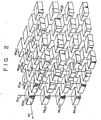
- Fig. 1 there is schematically illustrated a dynamic RAM of the laminar semi- conductor memory according to one preferred embodiment of the present invention.
- Semiconductive layers 10b, 10c, 10d, .,. are sequentially stacked and formed on a semiconductor layer or substrate 10a.
- a plurality of memory cells 12 formed, for example, of MOSFETS are formed in a matrix shape on the surface of each of semiconductor layers 10a, 10b, 10c, 10d, ....
- the semiconductor layers 10a, 10b, 10c, 10d, ... are electrically insulated from each other by electrically insulative layers 14a, 14b, 14c,....
- a two-dimensional (planar) memory cell array 12 is formed on the semiconductor layer 10a, and a second semiconductor layer 10b is formed on the insulating layer 14a formed on the array 12a.
- the planar memory cell arrays 12a, 12c, 12d, ... are respectively formed on the semiconductor layers 10b, 10c, 10d,... similarly to the above and electrically insulated from each other by insulating layers 14.
- the letter “i” designates the row number of the planar cell array formed on one of the semiconductor layers.
- the letter “j” denotes the column number of the planar cell arrays.
- the memory cells included in the planar memory cell array 12d formed on the semiconductive layer 10d drawn to be disposed at the uppermost stage are connected to a word line W1.
- the memory cells M 111' M 121 , ... forming the first row of a plurality of memory cells included in the planar cell array 12d and arranged in matrix shape are connected commonly to the word line W11'
- the word line w 11 is formed in accordance with the prior art to extend substantially in parallel with the surface of the layer 10d.
- the linear cell array, formed of memory cells M 211 , M 221 , ... forming the second row of the memory cells included in the planar cell array 12d, is connected commonly to the word line w 21 .
- all the linear row cell arrays included in the planar matrix array 12d are respectively connected commonly to the word lines W 31 ,....
- the word lines w 11 , w 21 , w 31 , ... are combined with the single word line (parent word line) W1 at the position in the vicinity of the planar cell array 12d substantially out of the planar cell array 12d.
- one word line W1 is branched to a plurality of word lines w 11 , w 21 , W 31 ,... at the above described predetermined position, and the branched word lines w 11 , w 21 , w 31 , ...
- the word line W1 and a plurality of word lines w 11 , w 21 , W 31 ,... branched from the parent word line W1 are included in an imaginary plane substantially parallel to the surface of the semiconductive layer 10d.
- a plurality of word lines w 21 , w 22 , W32 , ... are each connected in the similar manner to the above to a plurality of linear row cell arrays of planar cell array 12c formed on the semiconductive layer 10c formed to be electrically isolated by the insulating layer 14b from the layer 10c under the semiconductive layer 10d.
- These word lines W 12 , W 22 , W 32 ,... are combined with one parent word line W2.
- the word lines W3, W4 are connected to the other planar cell arrays 12b, 12a.
- the connecting state of the word lines are understood more clearly with reference to the model view of the semiconductor memory exploded and designated virtually in the respective memory cells in Fig. 2.
- bit lines B are further connected to the above-described memory cell structure connected with the above word lines W1, W2, W3, W4. These bit lines B substantially extend perpendicularly to the branched word line patterns.
- the bit line B 11 of the bit lines B ij , for example, connects commonly one memory cell M 111 , included in the planar cell array 12d, a memory cell M 112 included in the planar cell array 12c and disposed directly under the memory cell M 111 , a memory cell M 113 included in the planar cell array 12b and disposed directly under the memory cell M 112 , and a memory cell M 114 included in the planar cell array 12a and disposed directly under the memory cell M 113 through the semiconductor layers 10d, 10c, 10b.
- the connecting state of the memory cell structure of the bit line B 11 is further clarified with reference to Fig. 2.
- the other bit lines including the bit lines B 12 and bit lines B 21 , ... are provided substantially perpendicularly crossed to the word line patterns or the planar cell array 12 in the similar manner to the above.
- the memory cells M 11k , M 12k , M 21k , M 22k formed respectively on the same semi- conductor layers 12 of the memory cells of the semiconductor memory in Fig. 1 are eventually respectively connected commonly to the parent word lines W1, W2, W3, W4.
- M hj4 , ... having the same row number and column number and formed on the different semiconductor layer are respectively connected commonly to the bit lines B 11 , B 12 , ..., B 21 , B 22 , .... Accordingly, when an address signal is supplied, one word line of the above word lines Wk is activated in response to the signal.
- one word line e.g., word line W1
- all the memory cells M ij1 included in the planar cell array 12d connected to the word line W1 is activated and the transfer gates thereof are caused to open.
- the digital data stored as described above in the memory cell M 121 can be read out by designating the bit line B 12 at desired time similarly.
- the memory cells M ijk are arranged three dimensionally or stereoscopically, and one planar cell array formed on the same semiconductor layer is connted commonly to the same word line Wk.
- the bit lines B ij extend substantially perpendicularly to the word line pattern and connect commonly the memory cells M ij1 , M Ij2 , ..., M ijk , ... having the same row number and column number and formed on the different layers. Accordingly, the memory capacity can be increased as compared with the conventional memory element formed of the memory cells formed in two-dimensional manner on one semiconductive layer. Further, since the region cab- able of connecting the bit line for the stacked cell structure extends planarly, a number of bit lines may be readily connected to the stacked cell structure. This is convenient for the data sorting or image information processing.
- the word lines branched from one parent word line determines one virtual plane, to be named word-line routing plane, in which all the word lines branched from one parent word line are involved.
- the word lines w " , W 21 , w 31 , ... which are branched from the parent word line W1 determines one word-line routing plane, say P 1 , in which the word lines w 11 , w 21 , w 31 , ... are involved.
- the word lines W12 , w 22 , w 32 , ... are involved. More generally, the word lines w 1k , w 2k . w 3k , ... which are branched from the parent word line Wk determines one word-line routing plane P k in which the word lines w 1k , W 2k , w 3k , ... are involved. All these word-line routing planes P 1 , P 2 , ... which are assigned to parent word lines W1, W2, ..., respectively, are stacked and superposed substantially parallel to one another so that the word lines w 11 , w 12 , w 13 , ...
- word lines w 11 , w 12 , w 13 , ... determine one second word-line routing plane Q 1 in which all the word lines belonging to the same row number "i" are involved, and all the second word-line routing planes Q,'s are substantially orthogonal to the first word-line routing planes Pk's.
- Bit lines B ij are situated substantially perpendicularly to all the first word-line routing planes Pk's.
- both word lines and bit lines are arranged in two-dimensional manner, that is to say, word lines are substantially arranged in one plane while bit lines are substantially arranged in another plane, and both planes are superposed parallel to each other or substantially form one common plane.
- word lines and bit lines are arranged mutually in three-dimensional manner as described above in detail, and this three-dimensional routing scheme makes it possible to connect a much larger number of bit lines for an ensemble of memory cells than the conventional two-dimensional routing scheme does.
- a plurality of word lines w ik drawn from each of the planar cell arrays are combined respectively with the parent word lines Wk corresponding to the number of the planar cell arrays.
- the memory cells included in the each planar cell array are respectively branched and connected commonly to one of the parent word lines Wk.
- total word line length can be shortened, and hence the delay of the signal propagation speed can be reduced even at the terminal.
- the bit lines B ij are not necessarily laid complicatedly among the cells, the line length can be shortened. Therefore, the operating speed of the memory element can be improved.
- Fig. 3 illustrates one of the cell groups of a series of memory cells having the same row number and column number and formed in different planar cell array 12 in the memory cell structure of Fig. 2 particularly extracted.
- memory cells M 111 , M 112 , M113, M 114 are selected, and word lines w 11 , W 12 , W 13 , W 14 are respectively connected to these memory cells.
- each of the memory cells M 111 , M 112 , M 113 , M 114 includes one MOSFET and one capacitor.
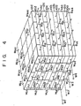
- Fig. 4 illustrates a dynamic RAM similar to that of prior art (GB-A-1 300881) wherein the like reference numerals designate the same or equivalent parts and components in Figs. 1 and 2, and will be omitted in description.
- the same bit line B ij (e.g., bit line B 11 ) is connected commonly to a series of memory cells (e.g., memory cells M 111 , M 211 , M 311 , M 411 ) having the same column number formed on the same semiconductor layer (e.g., layer 10d) in a plurality of memory cells M ijk included in the RAM in Fig. 4. Accordingly, a series of cells M 111 , M 211 , M 311 , M 411 , for example, are connected commonly to one bit line B 11 , a series of memory cells M 121 , M 221 , ... are connected to one bit line B 21 , a series of memory cells M 131 , M 231 , ...
- a series of memory cells M 111 , M 211 , M 311 , M 411 having the same column number formed on the same semiconductor layer (e.g., layer 10d) in a plurality of memory cells M ijk included in the RAM in Fig. 4.
- bit lines B 31 are connected to a bit line B 31 , and a series of memory cells M 141 , ..., M 441 are connected commonly to the bit line B 41 in the planar cell array 12d formed on the semiconductor layer 10d.
- These series of bit lines B 11 , B 21 , B 31 , B 4 extend substantially parallel to each other, and are formed substantially parallel to the planar cell array 12d formed on the semiconductor layer 10d.
- the memory cell M ij1 included in the planar cell array 12d is divided into a plurality of linear column cell arrays having the same column number and respectively connected commonly to the bit lines B J1'
- bit lines B 12 , B 22 , ..., bit lines B 13 , B 23 , ... and bit lines B 14 ,..., B 44 are connected commonly to a plurality of linear column cell arrays having the same column number in the same manner as above in the planar cell arrays 12c, 12b, 12a, respectively.
- a series of memory cells having the same row number of the memory cells included in each of planar cell arrays 12 are connected commonly to the same word lines w 1k .
- a plurality of word lines w 11 , w, 2 , w 13 , w 14 for respectively connecting a series of memory cell groups, each of which consists of linear cell arrays superposed to be elevationally aligned through the semiconductor layers 10, and insulating layers 14 are combined with one parent word line W1, W2, W3, W4.
- a word line w 11 for commonly connecting the linear row cell array of a series of memory cells M 111 , M 121 , M 131' M 141 having the same row number of the planar cell array 12d on the semiconductor layer 10d
- a word line w 12 for commonly connecting the memory cells M 112 , M 122 , M 132 , M 142 linearly extending in parallel with the linear row cell array under the memory cells M 111 , M 121 , M 131 , M 141 arranged linearly in series included in the planar cell array 12c
- word lines w 13 and w 14 for commonly connecting the memory cells M 113 , M 123 , ... and M 114 , M 124 , ...
- the line pattern formed of the word lines W 11 , W 12 , w 13 . w 14 branched from the parent word line W1 substantially intersect the planar cell arrays 12 or the above bit lines B formed respectively on the semiconductor layers 10.
- the word line patterns branched from each of parent word lines Wi substantially intersect the planar cell array or bit lines B formed respectively on the semiconductor layers 10. Therefore, to drive the RAM thus constructed, an address decoder 20 designated, for example, in Fig. 5 is employed.
- decoder elements 22 are provided correspondingly to the planar cell arrays 12a, 12b, 12c, 12d superposed in laminar or stacked state with each other as described above.
- Reference numerals A1, A2 denote address input lines, and reference numerals A1 , A2 designate inverting signal lines.
- the line pattern formed of these lines A1, A1, A2, A2 extend in parallel with each other and are included in a plane substantially perpendicular to the planar cell arrays 12 formed respectively on the semiconductor layers 10.
- Fig. 6 illustrates a circuit block section 23 particularly extracted correspondingly to the word lines W31 , W32 , W33 , w 34 in the above RAM (Fig. 4) of the address decoder 20 in Fig. 5.
- the parentwordline W3 combined with the word lines w 31 ,.... w 34 is activated when the digital levels of the address lines A1, A2 respectively become “0" and "1".
- the stereoscopic circuit in Fig. 6 includes n-channel type FETs 24, 26 and p-channel type FETs 24', 26' to form 2-input C-MOS NOR circuit. "High" power voltage V DD is supplied to the first power line 28 connected to the p-channel type FET 24'.
- V ss is applied to the second power line 30 connected to the n-channel type FETs 24, 26.
- electrically conductive connect lines L for electrically connecting between the FETs are shaded only for the purpose of readily distinguishing visually from the other section.
- n-channel type FETs 24 and 26 are connected in parallel with each other via the connect lines L1 and L2.
- the p-channel type FETs 24' and 26' are connected in series with each other via connect line L3.
- the connect line L4 connects between the n-channel type FET 26 and the p-channel type FET 26'.
- the FETs 24 and 24' are driven by the signal supplied from the input line A1, and the other FETs 26 and 26' are driven by the signal supplied from the inverting signal line A2.
- No FET is provided in the circuit structure 23 in Fig. 6 corresponding to the remaining inverting signal line A1 and input line A2.
- An equivalent circuit of the section of the address decoder in Fig. 6 thus constructed is shown in Fig. 7.
- the word lines w 31 , ..., w 34 are activated when the address input (A1, A2) becomes (0, 1).
- the word lines W31 , ..., w 34 are connected directly to one connect line L2 for connecting between the FETs 24 and 26 included in the decoder of Fig. 6 in their drain regions.
- the connect line L2 included in the address decoder substantially serves as the above-described parent word line W3. Accordingly, it is not necessary to newly provide a parent word line W3. It is not necessary by the same reason to newly provide other parent word lines W1, W2, W4. Therefore, the connection between the RAM in Fig. 4 and the address decoder in Fig. 5 can be efficiently performed, and the total line length can be shortened, thereby improving the signal propagation speed.
- the dynamic RAM is shown and described.
- the present invention is not limited to the particular RAM, but may also be applied for other memory elements such as, for example, a static memory, a read-only memory, etc.
- Fig. 8 illustrates one of the cell groups of a series of memory cells having the same row number and column number and formed in different planar cell array in the static type memory cell structure according to a modification of the preferred embodiment of the invention of Fig. 1 particularly extracted.
- memory cells M' 111 , M' 112 , M'113, M' 114 are selected, and word lines w , 11 , w' 12 , w' 13 , W ' 14 are respectively connected to these memory cells.
- word lines w , 11 , w' 12 , w' 13 , W ' 14 are respectively connected to these memory cells.
- each of the memory cells M' 111 , M' 112 , M' 113 , M' 114 is applied with a flip-flop formed of MOSFETs, and a pair of bit lines B 11 and B 11 are used as these memory cells. Voltage signals different from each other are supplied to these bit lines B 11 and B 11 .
Description
- The present invention relates to semiconductor memories and, more particularly, to a sterosocopic semi-conductor memory formed by stacking a plurality of semiconductor layers.
- A semiconductor memory including a read-only memory (ROM) and a random access memory (RAM) normally has a plurality of memory cells formed on the same plane or surface of a substrate. These memory cells are arrayed in a matrix shape on the surface of the substrate. One linear memory cell array arranged in a row direction of the memory cell matrix is connected commonly to one word line. Similarly, the remaining linear memory cell arrays arranged in the row direction are commonly connected to word lines. On the other hand, the linear memory cell array arranged in a column direction of the memory cell matrix is connected commonly to one bit line. The remaining memory cell arrays arranged in the column direction are similarly connected commonly to the bit lines, respectively. The above-described plurality of word lines and bit lines extend substantially on the same plane or surface on the substrate. More particularly, the word lines and bit lines extend on the plane in parallel relation to the memory cell matrix. The word lines extend in parallel with each other, while bit lines extend in parallel with each other. In other words, the every memory cell is connected to one word line and one bit line corresponding to the intersection between the word line and the bit line.
- When an address signal is inputted to the semiconductor memory, e.g., a dynamic RAM and one word line of the word lines is activated in response to the signal, transfer gates of a plurality of memory cells, contained in the memory cell array connected commonly to the word line, are opened. In this manner, the memory content stored at least one desired memory cell of the memory cells opened at the transfer gates thereof is read by the bit line, or the data supplied to the bit lines can be written or stored in the memory cell opened at the transfer gate thereof.
- According to an ordinary semiconductor memory thus composed, since a number of memory cells are arranged substantially on the same plane, the integration determined in response to the area of the surface of the substrate is restricted to a predetermined upper limit. When the memory integration exceeding the upper limit is necessary, it is required to increase the area of the semiconductor substrate, and the profile of a memory cell is undesirably enlarged. In this case, the lengths of the word lines and the bit lines also become lengthened, with the result that a delay of a signal propagation undesirably takes place.
- According further to the above-mentioned ordinary semiconductor memory, the number of bit lines to be provided also has a limit. In the above-described dynamic RAM, one bit line may be provided in one memory array extending in the column direction of the memory cell matrix. However, in case of a static RAM, normal and reverse potentials are necessary for one memory array of the column direction as readily understood by those skilled in the art to which the present invention pertains, two bit lines are necessarily provided for each column memory array. Thus, according to the conventional memory configuration, it is difficult to always obtain sufficient space for such bit lines. This becomes a serious problem in case of sorting the memory content or in case of employing the static RAM as an associative memory. If the allowable number of bit lines capable of forming on the same plane or surface is less than the number of bit lines to be originally necessary, data reading/ writing operation should be, in case of large quantity of necessary memory content, sequentially respectively carried out from the end of the memory cell matrix. As a consequence, the time required to read/write the data is increased, and the operating speed of the memory cell is undesirably decreased. Accordingly, the use of such memory cells is limited. For example, this memory cannot be used for the field which indpensably requires high operating speed in the memory such as picture information processing.
- From GB-A-1300881 (=FR-A-2 088 490, a stacked arrangement of two or more semiconductor bodies is known in which each semiconductor body has a plurality of storage elements thereon. Each semiconductor body has four address lines on one edge and further four address lines on a perpendicular edge for addressing individual ones of the semiconductor storage elements. For the supply of data, so-called "digit conductors" are connected in pairs to the respective semiconductor bodies. Each individual semiconductor element is thus identified by use of the address lines and data is supplied in common to all the semiconductor elements on each body via the respective pair of bit lines. This technique is specifically designed to avoid the need for lines to pass through the center of the semiconductor bodies. Furthermore, the disclosed structure is designed to reduce the number of connecting wiring lines as much as possible. According to the disclosed teaching, both word lines and bit lines for a two dimensional cell matrix formed on each semiconductor body are formed horizontally on the semiconductor layer surface.
- No decoder device for use with the stacked semiconductor storage array is disclosed in GB-A-1300881.
- An object of the present invention is to provide a new and improved semiconductor memory which has a large memory capacity and a fast operating speed.
- According to one aspect of the present invention there is provided a semiconductor memory having a plurality of semiconductor layers sequentially stacked with each other to form a laminar structure, a plurality of memory cells formed on each of said semiconductor layers in a matrix form, and a plurality of insulative layers each sandwiched between the respective semi- conductor layers for electrical insulation therebetween, characterised in that said memory device comprises:
- a plurality of word lines each assigned to a corresponding semiconductor layer to commonly couple the memory cells on that semiconductor layer; and
- a number of bit lines each of which electrically connects a set of memory cells which are formed on said semiconductor layers respectively and are stacked one above another in a direction substantially perpendicular to surfaces of said semi- conductor layers and said insulative layers, which are alternatingly stacked on one another, said bit lines running through said semiconductor layers and said insulative layers to allow electrical signals to be transferred through said semiconductor and insulative layers.
- According to a further aspect of the invention there is provided a semiconductor memory system comprising a semiconductor memory and decoder means for receiving an address input signal and for activating desired memory cells of said semiconductor memory, wherein said semi- conductor memory comprises a plurality of layers electrically isolated from each other and sequentially stacked to form a laminar structure, a plurality of cell matrix structures having a plurality of memory cells aligned in row and column directions on the surfaces of said layers, a plurality of bit lines for commonly connecting a plurality of the first linear memory cell arrays respectively formed of memory cells arranged in the same column direction of the memory cells included in the cell matrix structure on each of said layers and a plurality of word lines for commonly connecting a plurality of second linear memory cell arrays formed of memory cells arranged in the same row direction of the memory cells included in the memory cell matrix structure on each of said layers and substantially orthogonally intersecting the first linear memory cell arrays, characterized in that said decoder means is electrically connected through said word lines to said semiconductor memory, stacked correspondingly to laminar units formed respectively of said plurality of second linear memory cell arrays stacked via said layers and formed by arranging in parallel with each other a plurality of linear decoder element arrays respectively formed of a plurality of stacked decoder elements including active elements, each of said linear decoder element arrays including wiring means for commonly connecting said plurality of word lines which respectively connect a plurality of second linear memory cell arrays stacked with each other and included in each of said laminar units corresponding to the linear decoder element array and for connecting between predetermined said active elements provided therein, said wiring means extending to substantially orthogonally intersect said layers.
- The present invention is best uderstood by reference to the accompanying drawings, of which:
- Fig. 1 is a perspective view showing a part of dynamic random access memory (RAM) having stereoscopic memory cell structure according to one preferred embodiment of the present invention in a model;
- Fig. 2 is a perspective view clearly showing the wires of word lines and bit lines of the RAM in Fig. 1;
- Fig. 3 is a view enlargedly showing one of the linear memory cell arrays having the same row number and column number of the memory cells included in the RAM in Fig. 1 and superposed with each other via semiconductor layers;
- Fig. 4 is a perspective view showing a part of the dynamic RAM similar to that of prior art (GB-A-1300881);
- Fig. 5 is a perspective view schematically showing a part of the RAM configuration in Fig. 4 as one example of an address decoder having a laminar structure for the RAM in Fig. 4;
- Fig. 6 is a perspective view showing the internal configuration of a part of the address decoder in Fig. 5;
- Fig. 7 is a diagram showing an equivalent circuit of the circuit arrangement in Fig. 6; and
- Fig. 8 is a view showing one of the linear memory cell arrays having the same row number and column number of the memory cells included in a static RAM according to a modification of the dynamic RAM of Fig. 1, each of the memory cells being included in the linear memory cell formed of flip-flops and the cells being connected commonly to a pair of bit lines.
- Referring now to Fig. 1, there is schematically illustrated a dynamic RAM of the laminar semi- conductor memory according to one preferred embodiment of the present invention. In Fig. 1, only a part of the semiconductor memory is extracted and shown to readily understand the present invention.
Semiconductive layers 10b, 10c, 10d, .,. are sequentially stacked and formed on a semiconductor layer or substrate 10a. A plurality ofmemory cells 12 formed, for example, of MOSFETS are formed in a matrix shape on the surface of each ofsemiconductor layers 10a, 10b, 10c, 10d, .... Thesemiconductor layers 10a, 10b, 10c, 10d, ... are electrically insulated from each other by electricallyinsulative layers 14a, 14b, 14c,.... In other words, a two-dimensional (planar)memory cell array 12 is formed on the semiconductor layer 10a, and asecond semiconductor layer 10b is formed on the insulating layer 14a formed on the array 12a. The planarmemory cell arrays 12a, 12c, 12d, ... are respectively formed on thesemiconductor layers 10b, 10c, 10d,... similarly to the above and electrically insulated from each other by insulating layers 14. - To suitably show the memory cells arranged in three-dimensional and hence stereoscopical manner, one of memory cells is represented by Milk (i=1, 2, 3,..., j=1, 2, 3, ..., k=1, 2, 3, ...). The letter "i" designates the row number of the planar cell array formed on one of the semiconductor layers. The letter "j" denotes the column number of the planar cell arrays. The letter "k" designates the number of the planar cell arrays superposed in laminar state, and in Fig. 1, the planar cell array disposed on the uppermost layer is denoted by k=1.
- In Fig. 1, the memory cells included in the planar
memory cell array 12d formed on the semiconductive layer 10d drawn to be disposed at the uppermost stage are connected to a word line W1. The memory cells M111' M121, ... forming the first row of a plurality of memory cells included in theplanar cell array 12d and arranged in matrix shape are connected commonly to the word line W11' The word line w11 is formed in accordance with the prior art to extend substantially in parallel with the surface of the layer 10d. The linear cell array, formed of memory cells M211, M221, ... forming the second row of the memory cells included in theplanar cell array 12d, is connected commonly to the word line w21. Similarly to the above, all the linear row cell arrays included in theplanar matrix array 12d are respectively connected commonly to the word lines W31,.... The word lines w11, w21, w31, ... are combined with the single word line (parent word line) W1 at the position in the vicinity of theplanar cell array 12d substantially out of theplanar cell array 12d. In other words, one word line W1 is branched to a plurality of word lines w11, w21, W31,... at the above described predetermined position, and the branched word lines w11, w21, w31, ... are electrically commonly connected between the memory cells linearly arranged in the row direction of a plurality of memory cells included in theplanar cell array 12d. The word line W1 and a plurality of word lines w11, w21, W31,... branched from the parent word line W1 are included in an imaginary plane substantially parallel to the surface of the semiconductive layer 10d. - A plurality of word lines w21, w22, W32, ... are each connected in the similar manner to the above to a plurality of linear row cell arrays of planar cell array 12c formed on the semiconductive layer 10c formed to be electrically isolated by the insulating
layer 14b from the layer 10c under the semiconductive layer 10d. These word lines W12, W22, W32,... are combined with one parent word line W2. Similarly to the above, the word lines W3, W4 are connected to the otherplanar cell arrays 12b, 12a. The connecting state of the word lines are understood more clearly with reference to the model view of the semiconductor memory exploded and designated virtually in the respective memory cells in Fig. 2. - In Fig. 1, a plurality of bit lines B are further connected to the above-described memory cell structure connected with the above word lines W1, W2, W3, W4. These bit lines B substantially extend perpendicularly to the branched word line patterns. In other words, each of bit lines B1j (i=1, 2,3,... , j=1, 2, 3, ...) is perpendicularly extended to the
planar cell arrays 12 each formed on the semiconductor layers 10, and connected commonly to the stacked memory cell group arranged to be linearly aligned to each other in a direction substantially perpendicularly to one of the planarmemory cell arrays 12. The bit line B11, of the bit lines Bij, for example, connects commonly one memory cell M111, included in theplanar cell array 12d, a memory cell M112included in the planar cell array 12c and disposed directly under the memory cell M111, a memory cell M113 included in theplanar cell array 12b and disposed directly under the memory cell M112, and a memory cell M114 included in the planar cell array 12a and disposed directly under the memory cell M113 through thesemiconductor layers 10d, 10c, 10b. The connecting state of the memory cell structure of the bit line B11, is further clarified with reference to Fig. 2. The other bit lines including the bit lines B12 and bit lines B21, ... are provided substantially perpendicularly crossed to the word line patterns or theplanar cell array 12 in the similar manner to the above. - In other words, the memory cells M11k, M12k, M21k, M22k formed respectively on the same semi-
conductor layers 12 of the memory cells of the semiconductor memory in Fig. 1 are eventually respectively connected commonly to the parent word lines W1, W2, W3, W4. On the other hand, the memory cells Mij1 Mij2, ..., and Mij3. Mhj4, ... having the same row number and column number and formed on the different semiconductor layer are respectively connected commonly to the bit lines B11, B12, ..., B21, B22, .... Accordingly, when an address signal is supplied, one word line of the above word lines Wk is activated in response to the signal. Therefore, when one word line, e.g., word line W1, is activated, all the memory cells Mij1, included in theplanar cell array 12d connected to the word line W1 is activated and the transfer gates thereof are caused to open. In this state, at least one bit line B1j=Bl2 is designated for one desired memory cell, e.g., M121 of these memory cells Mij1' the digital data supplied to the bit line B12 can be written. The digital data stored as described above in the memory cell M121 can be read out by designating the bit line B12 at desired time similarly. - According to the dynamic RAM as one preferred embodiment of the present invention thus constructed, the memory cells Mijk are arranged three dimensionally or stereoscopically, and one planar cell array formed on the same semiconductor layer is connted commonly to the same word line Wk. The bit lines Bij extend substantially perpendicularly to the word line pattern and connect commonly the memory cells Mij1, MIj2, ..., Mijk, ... having the same row number and column number and formed on the different layers. Accordingly, the memory capacity can be increased as compared with the conventional memory element formed of the memory cells formed in two-dimensional manner on one semiconductive layer. Further, since the region cab- able of connecting the bit line for the stacked cell structure extends planarly, a number of bit lines may be readily connected to the stacked cell structure. This is convenient for the data sorting or image information processing.
- In other words, in the stacked memory cell structure shown in Figs. 1 and 2 and described in detail above, the word lines branched from one parent word line determines one virtual plane, to be named word-line routing plane, in which all the word lines branched from one parent word line are involved. The word lines w", W21, w31, ... which are branched from the parent word line W1 determines one word-line routing plane, say P1, in which the word lines w11, w21, w31, ... are involved. The word lines w12, w22, W32, ... which are branched from the parent word line W2 determined one word-line routing plane, say P2, in which the word lines W12, w22, w32, ... are involved. More generally, the word lines w1k, w2k. w3k, ... which are branched from the parent word line Wk determines one word-line routing plane Pk in which the word lines w1k, W2k, w3k, ... are involved. All these word-line routing planes P1, P2, ... which are assigned to parent word lines W1, W2, ..., respectively, are stacked and superposed substantially parallel to one another so that the word lines w11, w12, w13, ... which belong to the same row number "i" but to different word-line routing planes P1, P2, P3, ..., respectively, are superposed to one after another. In other words, the word lines w11, w12, w13, ... determine one second word-line routing plane Q1 in which all the word lines belonging to the same row number "i" are involved, and all the second word-line routing planes Q,'s are substantially orthogonal to the first word-line routing planes Pk's. Bit lines Bij are situated substantially perpendicularly to all the first word-line routing planes Pk's. In the conventional memory cell array structure formed in two-dimensional manner on one semiconductor layer, both word lines and bit lines are arranged in two-dimensional manner, that is to say, word lines are substantially arranged in one plane while bit lines are substantially arranged in another plane, and both planes are superposed parallel to each other or substantially form one common plane. In the stacked memory cell structure shown in Figs. 1 and 2, word lines and bit lines are arranged mutually in three-dimensional manner as described above in detail, and this three-dimensional routing scheme makes it possible to connect a much larger number of bit lines for an ensemble of memory cells than the conventional two-dimensional routing scheme does.
- Further, a plurality of word lines wik drawn from each of the planar cell arrays are combined respectively with the parent word lines Wk corresponding to the number of the planar cell arrays. In other words, the memory cells included in the each planar cell array are respectively branched and connected commonly to one of the parent word lines Wk. In this manner, total word line length can be shortened, and hence the delay of the signal propagation speed can be reduced even at the terminal. Further, since the bit lines Bij are not necessarily laid complicatedly among the cells, the line length can be shortened. Therefore, the operating speed of the memory element can be improved.
- Fig. 3 illustrates one of the cell groups of a series of memory cells having the same row number and column number and formed in different
planar cell array 12 in the memory cell structure of Fig. 2 particularly extracted. For the purpose of illustration only, memory cells M111, M112, M113, M114 are selected, and word lines w11, W12, W13, W14 are respectively connected to these memory cells. In Fig. 3, each of the memory cells M111, M112, M113, M114 includes one MOSFET and one capacitor. - Fig. 4 illustrates a dynamic RAM similar to that of prior art (GB-A-1 300881) wherein the like reference numerals designate the same or equivalent parts and components in Figs. 1 and 2, and will be omitted in description.
- The same bit line Bij (e.g., bit line B11) is connected commonly to a series of memory cells (e.g., memory cells M111, M211, M311, M411) having the same column number formed on the same semiconductor layer (e.g., layer 10d) in a plurality of memory cells Mijk included in the RAM in Fig. 4. Accordingly, a series of cells M111, M211, M311, M411, for example, are connected commonly to one bit line B11, a series of memory cells M121, M221, ... are connected to one bit line B21, a series of memory cells M131, M231, ... are connected to a bit line B31, and a series of memory cells M141, ..., M441 are connected commonly to the bit line B41 in the
planar cell array 12d formed on the semiconductor layer 10d. These series of bit lines B11, B21, B31, B4, extend substantially parallel to each other, and are formed substantially parallel to theplanar cell array 12d formed on the semiconductor layer 10d. In other words, the memory cell Mij1 included in theplanar cell array 12d is divided into a plurality of linear column cell arrays having the same column number and respectively connected commonly to the bit lines BJ1' - The bit lines B12, B22, ..., bit lines B13, B23, ... and bit lines B14,..., B44 are connected commonly to a plurality of linear column cell arrays having the same column number in the same manner as above in the
planar cell arrays 12c, 12b, 12a, respectively. - On the other hand, a series of memory cells having the same row number of the memory cells included in each of
planar cell arrays 12 are connected commonly to the same word lines w1k. Further, a plurality of word lines w11, w,2, w13, w14 for respectively connecting a series of memory cell groups, each of which consists of linear cell arrays superposed to be elevationally aligned through the semiconductor layers 10, and insulating layers 14 are combined with one parent word line W1, W2, W3, W4. For example, in Fig. 4, a word line w11, for commonly connecting the linear row cell array of a series of memory cells M111, M121, M131' M141 having the same row number of theplanar cell array 12d on the semiconductor layer 10d, a word line w12 for commonly connecting the memory cells M112, M122, M132, M142 linearly extending in parallel with the linear row cell array under the memory cells M111, M121, M131, M141 arranged linearly in series included in the planar cell array 12c, and word lines w13 and w14 for commonly connecting the memory cells M113, M123, ... and M114, M124, ... superposed with the memory cells M111, M121, M131, M141 forming the linear cell arrays included in theplanar cell arrays 12b, 12a are combined with one parent word line W1. In other words, the line pattern formed of the word lines W11, W12, w13. w14 branched from the parent word line W1 substantially intersect theplanar cell arrays 12 or the above bit lines B formed respectively on the semiconductor layers 10. - Other series of word lines W21, ..., w24 are similarly combined with one parent word line W2. Further, other series of word lines w31, ..., w34 and the other series of word lines w41, ..., w44 are respectively combined with the parent word lines W3 and W4.
- In this manner, even in the stereoscopic memory cell structure connected to the bit lines Bjk and word lines Wi, the writing/reading of the digital data can be carried out similarly to the above-described embodiments.
- According to the dynamic RAM in Fig. 4, the word line patterns branched from each of parent word lines Wi substantially intersect the planar cell array or bit lines B formed respectively on the semiconductor layers 10. Therefore, to drive the RAM thus constructed, an
address decoder 20 designated, for example, in Fig. 5 is employed. - According to the address decoder in Fig. 5,
decoder elements 22 are provided correspondingly to theplanar cell arrays A1 ,A2 designate inverting signal lines. The line pattern formed of these lines A1, A1, A2, A2 extend in parallel with each other and are included in a plane substantially perpendicular to theplanar cell arrays 12 formed respectively on the semiconductor layers 10. - Fig. 6 illustrates a
circuit block section 23 particularly extracted correspondingly to the word lines W31, W32, W33, w34 in the above RAM (Fig. 4) of theaddress decoder 20 in Fig. 5. The parentwordline W3 combined with the word lines w31,.... w34 is activated when the digital levels of the address lines A1, A2 respectively become "0" and "1". The stereoscopic circuit in Fig. 6 includes n-channel type FETs first power line 28 connected to the p-channel type FET 24'. "Low" power voltage Vss is applied to thesecond power line 30 connected to the n-channel type FETs channel type FETs channel type FET 26 and the p-channel type FET 26'. Accordingly, theFETs 24 and 24' are driven by the signal supplied from the input line A1, and theother FETs 26 and 26' are driven by the signal supplied from the inverting signal line A2. No FET is provided in thecircuit structure 23 in Fig. 6 corresponding to the remaining inverting signal line A1 and input line A2. An equivalent circuit of the section of the address decoder in Fig. 6 thus constructed is shown in Fig. 7. - According to the
circuit structure 23 of a part of the address decoder thus constructed, the word lines w31, ..., w34 are activated when the address input (A1, A2) becomes (0, 1). In this state, the word lines W31, ..., w34are connected directly to one connect line L2 for connecting between theFETs - Although the parent invention has been shown and described with respect to particular embodiments, nevertheless, various changes and modifications which are obvious to a person skilled in the art to which the invention pertains are deemed to lie within the spirit, scope, and contemplation of the invention. In the embodiments described above, the dynamic RAM is shown and described. However, the present invention is not limited to the particular RAM, but may also be applied for other memory elements such as, for example, a static memory, a read-only memory, etc.
- Fig. 8 illustrates one of the cell groups of a series of memory cells having the same row number and column number and formed in different planar cell array in the static type memory cell structure according to a modification of the preferred embodiment of the invention of Fig. 1 particularly extracted. For the purpose of illustration only, memory cells M'111, M'112, M'113, M'114 are selected, and word lines w, 11, w'12, w'13, W'14 are respectively connected to these memory cells. In Fig. 8, each of the memory cells M'111, M'112, M'113, M'114 is applied with a flip-flop formed of MOSFETs, and a pair of bit lines B11 and
B 11 B 11 .
Claims (5)
Applications Claiming Priority (2)
| Application Number | Priority Date | Filing Date | Title |
|---|---|---|---|
| JP56136399A JPS5837948A (en) | 1981-08-31 | 1981-08-31 | Laminated semiconductor memory device |
| JP136399/81 | 1981-08-31 |
Publications (3)
| Publication Number | Publication Date |
|---|---|
| EP0073486A2 EP0073486A2 (en) | 1983-03-09 |
| EP0073486A3 EP0073486A3 (en) | 1986-03-26 |
| EP0073486B1 true EP0073486B1 (en) | 1989-04-05 |
Family
ID=15174249
Family Applications (1)
| Application Number | Title | Priority Date | Filing Date |
|---|---|---|---|
| EP19820107858 Expired EP0073486B1 (en) | 1981-08-31 | 1982-08-26 | Stacked semiconductor memory |
Country Status (3)
| Country | Link |
|---|---|
| EP (1) | EP0073486B1 (en) |
| JP (1) | JPS5837948A (en) |
| DE (1) | DE3279599D1 (en) |
Cited By (6)
| Publication number | Priority date | Publication date | Assignee | Title |
|---|---|---|---|---|
| US6525953B1 (en) | 2001-08-13 | 2003-02-25 | Matrix Semiconductor, Inc. | Vertically-stacked, field-programmable, nonvolatile memory and method of fabrication |
| US6593624B2 (en) | 2001-09-25 | 2003-07-15 | Matrix Semiconductor, Inc. | Thin film transistors with vertically offset drain regions |
| US6624485B2 (en) | 2001-11-05 | 2003-09-23 | Matrix Semiconductor, Inc. | Three-dimensional, mask-programmed read only memory |
| US6731011B2 (en) | 2002-02-19 | 2004-05-04 | Matrix Semiconductor, Inc. | Memory module having interconnected and stacked integrated circuits |
| US7816189B2 (en) | 1998-11-16 | 2010-10-19 | Sandisk 3D Llc | Vertically stacked field programmable nonvolatile memory and method of fabrication |
| US8575719B2 (en) | 2000-04-28 | 2013-11-05 | Sandisk 3D Llc | Silicon nitride antifuse for use in diode-antifuse memory arrays |
Families Citing this family (46)
| Publication number | Priority date | Publication date | Assignee | Title |
|---|---|---|---|---|
| JPS6185858A (en) * | 1984-10-04 | 1986-05-01 | Nec Corp | Semiconductor memory |
| US4742474A (en) * | 1985-04-05 | 1988-05-03 | Tektronix, Inc. | Variable access frame buffer memory |
| JPS62208665A (en) * | 1986-03-07 | 1987-09-12 | Mitsubishi Electric Corp | Laminated type semiconductor memory |
| JPS62219550A (en) * | 1986-03-19 | 1987-09-26 | Sharp Corp | Semiconductor memory element |
| US5515267A (en) * | 1986-04-04 | 1996-05-07 | Alsenz; Richard H. | Apparatus and method for refrigeration system control and display |
| US5191643A (en) * | 1986-04-04 | 1993-03-02 | Alsenz Richard H | Method and apparatus for refrigeration control and display |
| EP0257987B1 (en) * | 1986-08-22 | 1991-11-06 | Fujitsu Limited | Semiconductor memory device |
| JPS63204595A (en) * | 1987-02-20 | 1988-08-24 | Fujitsu Ltd | Multi-plane video ram constituting system |
| JPS63245567A (en) * | 1987-03-31 | 1988-10-12 | Toshiba Corp | Picture processor |
| JP2778977B2 (en) * | 1989-03-14 | 1998-07-23 | 株式会社東芝 | Semiconductor device and manufacturing method thereof |
| EP0420339A3 (en) * | 1989-09-29 | 1992-06-03 | N.V. Philips' Gloeilampenfabrieken | Multi-plane random access memory system |
| US5227338A (en) * | 1990-04-30 | 1993-07-13 | International Business Machines Corporation | Three-dimensional memory card structure with internal direct chip attachment |
| US5099309A (en) * | 1990-04-30 | 1992-03-24 | International Business Machines Corporation | Three-dimensional memory card structure with internal direct chip attachment |
| EP0516866A1 (en) * | 1991-05-03 | 1992-12-09 | International Business Machines Corporation | Modular multilayer interwiring structure |
| US5818112A (en) * | 1994-11-15 | 1998-10-06 | Siemens Aktiengesellschaft | Arrangement for capacitive signal transmission between the chip layers of a vertically integrated circuit |
| US5701037A (en) * | 1994-11-15 | 1997-12-23 | Siemens Aktiengesellschaft | Arrangement for inductive signal transmission between the chip layers of a vertically integrated circuit |
| FR2745973B1 (en) * | 1996-03-08 | 1998-04-03 | Thomson Csf | MASS MEMORY AND METHOD FOR MANUFACTURING MASS MEMORY |
| US5915167A (en) * | 1997-04-04 | 1999-06-22 | Elm Technology Corporation | Three dimensional structure memory |
| EP1284017A4 (en) | 2000-04-28 | 2008-10-08 | Matrix Semiconductor Inc | Three-dimensional memory array and method of fabrication |
| EP2323164B1 (en) | 2000-08-14 | 2015-11-25 | SanDisk 3D LLC | Multilevel memory array and method for making same |
| US20030120858A1 (en) | 2000-09-15 | 2003-06-26 | Matrix Semiconductor, Inc. | Memory devices and methods for use therewith |
| US6486065B2 (en) | 2000-12-22 | 2002-11-26 | Matrix Semiconductor, Inc. | Method of forming nonvolatile memory device utilizing a hard mask |
| US6591394B2 (en) | 2000-12-22 | 2003-07-08 | Matrix Semiconductor, Inc. | Three-dimensional memory array and method for storing data bits and ECC bits therein |
| US6486066B2 (en) | 2001-02-02 | 2002-11-26 | Matrix Semiconductor, Inc. | Method of generating integrated circuit feature layout for improved chemical mechanical polishing |
| US7352199B2 (en) | 2001-02-20 | 2008-04-01 | Sandisk Corporation | Memory card with enhanced testability and methods of making and using the same |
| US6843421B2 (en) | 2001-08-13 | 2005-01-18 | Matrix Semiconductor, Inc. | Molded memory module and method of making the module absent a substrate support |
| EP1321941B1 (en) * | 2001-12-21 | 2005-08-17 | Kabushiki Kaisha Toshiba | Magnetic random access memory with stacked memory cells |
| US6853049B2 (en) | 2002-03-13 | 2005-02-08 | Matrix Semiconductor, Inc. | Silicide-silicon oxide-semiconductor antifuse device and method of making |
| US6643159B2 (en) | 2002-04-02 | 2003-11-04 | Hewlett-Packard Development Company, L.P. | Cubic memory array |
| US6687147B2 (en) * | 2002-04-02 | 2004-02-03 | Hewlett-Packard Development Company, L.P. | Cubic memory array with diagonal select lines |
| US6737675B2 (en) | 2002-06-27 | 2004-05-18 | Matrix Semiconductor, Inc. | High density 3D rail stack arrays |
| DE10308323B4 (en) * | 2003-02-26 | 2007-10-11 | Infineon Technologies Ag | Semiconductor chip arrangement with ROM |
| US7233024B2 (en) * | 2003-03-31 | 2007-06-19 | Sandisk 3D Llc | Three-dimensional memory device incorporating segmented bit line memory array |
| US6879505B2 (en) | 2003-03-31 | 2005-04-12 | Matrix Semiconductor, Inc. | Word line arrangement having multi-layer word line segments for three-dimensional memory array |
| WO2004100267A1 (en) * | 2003-04-03 | 2004-11-18 | Hewlett-Packard Development Company, L.P. | Cubic memory array |
| US7184289B2 (en) * | 2003-11-12 | 2007-02-27 | Intel Corporation | Parallel electrode memory |
| US7359279B2 (en) | 2005-03-31 | 2008-04-15 | Sandisk 3D Llc | Integrated circuit memory array configuration including decoding compatibility with partial implementation of multiple memory layers |
| US7272052B2 (en) | 2005-03-31 | 2007-09-18 | Sandisk 3D Llc | Decoding circuit for non-binary groups of memory line drivers |
| US7142471B2 (en) | 2005-03-31 | 2006-11-28 | Sandisk 3D Llc | Method and apparatus for incorporating block redundancy in a memory array |
| US7054219B1 (en) | 2005-03-31 | 2006-05-30 | Matrix Semiconductor, Inc. | Transistor layout configuration for tight-pitched memory array lines |
| US7420832B1 (en) * | 2007-04-30 | 2008-09-02 | International Business Machines Corporation | Array split across three-dimensional interconnected chips |
| US8907392B2 (en) * | 2011-12-22 | 2014-12-09 | Semiconductor Energy Laboratory Co., Ltd. | Semiconductor memory device including stacked sub memory cells |
| US8704221B2 (en) * | 2011-12-23 | 2014-04-22 | Semiconductor Energy Laboratory Co., Ltd. | Semiconductor device |
| US20150063039A1 (en) * | 2013-08-29 | 2015-03-05 | Taiwan Semiconductor Manufacturing Company Ltd. | Redundancy in stacked memory structure |
| US9875789B2 (en) | 2013-11-22 | 2018-01-23 | Taiwan Semiconductor Manufacturing Company, Ltd. | 3D structure for advanced SRAM design to avoid half-selected issue |
| US9478495B1 (en) | 2015-10-26 | 2016-10-25 | Sandisk Technologies Llc | Three dimensional memory device containing aluminum source contact via structure and method of making thereof |
Family Cites Families (3)
| Publication number | Priority date | Publication date | Assignee | Title |
|---|---|---|---|---|
| DE2022895B2 (en) * | 1970-05-11 | 1976-12-02 | Siemens AG, 1000 Berlin und 8000 München | STACKED ARRANGEMENT OF SEMICONDUCTOR BODIES AND PROCESS FOR THEIR PRODUCTION |
| DE2806685A1 (en) * | 1978-02-16 | 1979-08-23 | Siemens Ag | Stacked semiconductor structure using film mounting - comprises stack of substrates holding semiconductor chips connected to main substrate or circuit board with terminals |
| JPS5852345B2 (en) * | 1978-09-01 | 1983-11-22 | パイオニア株式会社 | Semiconductor device and its manufacturing method |
-
1981
- 1981-08-31 JP JP56136399A patent/JPS5837948A/en active Pending
-
1982
- 1982-08-26 EP EP19820107858 patent/EP0073486B1/en not_active Expired
- 1982-08-26 DE DE8282107858T patent/DE3279599D1/en not_active Expired
Cited By (12)
| Publication number | Priority date | Publication date | Assignee | Title |
|---|---|---|---|---|
| US7816189B2 (en) | 1998-11-16 | 2010-10-19 | Sandisk 3D Llc | Vertically stacked field programmable nonvolatile memory and method of fabrication |
| US7978492B2 (en) | 1998-11-16 | 2011-07-12 | Sandisk 3D Llc | Integrated circuit incorporating decoders disposed beneath memory arrays |
| US8208282B2 (en) | 1998-11-16 | 2012-06-26 | Sandisk 3D Llc | Vertically stacked field programmable nonvolatile memory and method of fabrication |
| US8503215B2 (en) | 1998-11-16 | 2013-08-06 | Sandisk 3D Llc | Vertically stacked field programmable nonvolatile memory and method of fabrication |
| US8897056B2 (en) | 1998-11-16 | 2014-11-25 | Sandisk 3D Llc | Pillar-shaped nonvolatile memory and method of fabrication |
| US9214243B2 (en) | 1998-11-16 | 2015-12-15 | Sandisk 3D Llc | Three-dimensional nonvolatile memory and method of fabrication |
| US8575719B2 (en) | 2000-04-28 | 2013-11-05 | Sandisk 3D Llc | Silicon nitride antifuse for use in diode-antifuse memory arrays |
| US6525953B1 (en) | 2001-08-13 | 2003-02-25 | Matrix Semiconductor, Inc. | Vertically-stacked, field-programmable, nonvolatile memory and method of fabrication |
| US6689644B2 (en) | 2001-08-13 | 2004-02-10 | Matrix Semiconductor, Inc. | Vertically-stacked, field-programmable, nonvolatile memory and method of fabrication |
| US6593624B2 (en) | 2001-09-25 | 2003-07-15 | Matrix Semiconductor, Inc. | Thin film transistors with vertically offset drain regions |
| US6624485B2 (en) | 2001-11-05 | 2003-09-23 | Matrix Semiconductor, Inc. | Three-dimensional, mask-programmed read only memory |
| US6731011B2 (en) | 2002-02-19 | 2004-05-04 | Matrix Semiconductor, Inc. | Memory module having interconnected and stacked integrated circuits |
Also Published As
| Publication number | Publication date |
|---|---|
| DE3279599D1 (en) | 1989-05-11 |
| EP0073486A2 (en) | 1983-03-09 |
| EP0073486A3 (en) | 1986-03-26 |
| JPS5837948A (en) | 1983-03-05 |
Similar Documents
| Publication | Publication Date | Title |
|---|---|---|
| EP0073486B1 (en) | Stacked semiconductor memory | |
| US4884115A (en) | Basic cell for a gate array arrangement in CMOS Technology | |
| EP0169332B1 (en) | High density one device memory | |
| JP2863661B2 (en) | Read-only memory | |
| EP0184464A1 (en) | Gate array integrated circuit device and production method therefor | |
| JPH04257260A (en) | Read-only memory integrated circuit | |
| JPH0870099A (en) | Mono-wtist layout for conductor pair of integrated circuit and method | |
| KR100314973B1 (en) | Global wire management apparatus and method for a multiple-port random access memory | |
| JPH0732195B2 (en) | Semiconductor integrated circuit | |
| US6362994B1 (en) | Memory architecture and decoder addressing | |
| US4780851A (en) | Semiconductor memory device having improved redundant structure | |
| US4910574A (en) | Porous circuit macro for semiconductor integrated circuits | |
| US5770874A (en) | High density semiconductor memory device | |
| US5377136A (en) | Semiconductor integrated circuit device with built-in memory circuit group | |
| US9812176B2 (en) | Memory structure | |
| US6067268A (en) | Redundancy fuse box and method for arranging the same | |
| US5182727A (en) | Array layout structure for implementing large high-density address decoders for gate array memories | |
| US5936875A (en) | Integrated circuit memory devices including overlapping power lines and bit lines | |
| US5535153A (en) | Semiconductor device | |
| US4584671A (en) | Semiconductor memories | |
| US5204842A (en) | Semiconductor memory with memory unit comprising a plurality of memory blocks | |
| KR910000877B1 (en) | Semiconductor memory device having common driver circuits for plural memory cell arrays | |
| EP0479274B1 (en) | Semiconductor memory device | |
| US4802121A (en) | Memory array with partitioned bit lines | |
| JPH0582746A (en) | Semiconductor memory device |
Legal Events
| Date | Code | Title | Description |
|---|---|---|---|
| PUAI | Public reference made under article 153(3) epc to a published international application that has entered the european phase |
Free format text: ORIGINAL CODE: 0009012 |
|
| 17P | Request for examination filed |
Effective date: 19820826 |
|
| AK | Designated contracting states |
Designated state(s): DE FR GB IT |
|
| RAP1 | Party data changed (applicant data changed or rights of an application transferred) |
Owner name: KABUSHIKI KAISHA TOSHIBA |
|
| PUAL | Search report despatched |
Free format text: ORIGINAL CODE: 0009013 |
|
| AK | Designated contracting states |
Kind code of ref document: A3 Designated state(s): DE FR GB IT |
|
| 17Q | First examination report despatched |
Effective date: 19870216 |
|
| GRAA | (expected) grant |
Free format text: ORIGINAL CODE: 0009210 |
|
| AK | Designated contracting states |
Kind code of ref document: B1 Designated state(s): DE FR GB IT |
|
| REF | Corresponds to: |
Ref document number: 3279599 Country of ref document: DE Date of ref document: 19890511 |
|
| ET | Fr: translation filed | ||
| ITF | It: translation for a ep patent filed |
Owner name: BUGNION S.P.A. |
|
| PLBE | No opposition filed within time limit |
Free format text: ORIGINAL CODE: 0009261 |
|
| STAA | Information on the status of an ep patent application or granted ep patent |
Free format text: STATUS: NO OPPOSITION FILED WITHIN TIME LIMIT |
|
| 26N | No opposition filed | ||
| ITTA | It: last paid annual fee | ||
| PGFP | Annual fee paid to national office [announced via postgrant information from national office to epo] |
Ref country code: FR Payment date: 19930805 Year of fee payment: 12 |
|
| PGFP | Annual fee paid to national office [announced via postgrant information from national office to epo] |
Ref country code: GB Payment date: 19930817 Year of fee payment: 12 |
|
| PGFP | Annual fee paid to national office [announced via postgrant information from national office to epo] |
Ref country code: DE Payment date: 19930823 Year of fee payment: 12 |
|
| PG25 | Lapsed in a contracting state [announced via postgrant information from national office to epo] |
Ref country code: GB Effective date: 19940826 |
|
| GBPC | Gb: european patent ceased through non-payment of renewal fee |
Effective date: 19940826 |
|
| PG25 | Lapsed in a contracting state [announced via postgrant information from national office to epo] |
Ref country code: FR Effective date: 19950428 |
|
| PG25 | Lapsed in a contracting state [announced via postgrant information from national office to epo] |
Ref country code: DE Effective date: 19950503 |
|
| REG | Reference to a national code |
Ref country code: FR Ref legal event code: ST |