EP0074719A2 - Imaging device - Google Patents
Imaging device Download PDFInfo
- Publication number
- EP0074719A2 EP0074719A2 EP82304252A EP82304252A EP0074719A2 EP 0074719 A2 EP0074719 A2 EP 0074719A2 EP 82304252 A EP82304252 A EP 82304252A EP 82304252 A EP82304252 A EP 82304252A EP 0074719 A2 EP0074719 A2 EP 0074719A2
- Authority
- EP
- European Patent Office
- Prior art keywords
- imaging device
- transistor
- reading
- elements
- circuits
- Prior art date
- Legal status (The legal status is an assumption and is not a legal conclusion. Google has not performed a legal analysis and makes no representation as to the accuracy of the status listed.)
- Granted
Links
Images


Classifications
-
- H—ELECTRICITY
- H04—ELECTRIC COMMUNICATION TECHNIQUE
- H04N—PICTORIAL COMMUNICATION, e.g. TELEVISION
- H04N1/00—Scanning, transmission or reproduction of documents or the like, e.g. facsimile transmission; Details thereof
- H04N1/024—Details of scanning heads ; Means for illuminating the original
- H04N1/02418—Details of scanning heads ; Means for illuminating the original for picture information pick up and reproduction
- H04N1/02463—Details of scanning heads ; Means for illuminating the original for picture information pick up and reproduction using heads mounted on the same support or substrate
-
- G—PHYSICS
- G03—PHOTOGRAPHY; CINEMATOGRAPHY; ANALOGOUS TECHNIQUES USING WAVES OTHER THAN OPTICAL WAVES; ELECTROGRAPHY; HOLOGRAPHY
- G03G—ELECTROGRAPHY; ELECTROPHOTOGRAPHY; MAGNETOGRAPHY
- G03G15/00—Apparatus for electrographic processes using a charge pattern
- G03G15/22—Apparatus for electrographic processes using a charge pattern involving the combination of more than one step according to groups G03G13/02 - G03G13/20
- G03G15/28—Apparatus for electrographic processes using a charge pattern involving the combination of more than one step according to groups G03G13/02 - G03G13/20 in which projection is obtained by line scanning
-
- H—ELECTRICITY
- H04—ELECTRIC COMMUNICATION TECHNIQUE
- H04N—PICTORIAL COMMUNICATION, e.g. TELEVISION
- H04N1/00—Scanning, transmission or reproduction of documents or the like, e.g. facsimile transmission; Details thereof
- H04N1/024—Details of scanning heads ; Means for illuminating the original
-
- H—ELECTRICITY
- H04—ELECTRIC COMMUNICATION TECHNIQUE
- H04N—PICTORIAL COMMUNICATION, e.g. TELEVISION
- H04N1/00—Scanning, transmission or reproduction of documents or the like, e.g. facsimile transmission; Details thereof
- H04N1/04—Scanning arrangements, i.e. arrangements for the displacement of active reading or reproducing elements relative to the original or reproducing medium, or vice versa
- H04N1/207—Simultaneous scanning of the original picture and the reproduced picture with a common scanning device
-
- H—ELECTRICITY
- H04—ELECTRIC COMMUNICATION TECHNIQUE
- H04N—PICTORIAL COMMUNICATION, e.g. TELEVISION
- H04N1/00—Scanning, transmission or reproduction of documents or the like, e.g. facsimile transmission; Details thereof
- H04N1/40—Picture signal circuits
- H04N1/40025—Circuits exciting or modulating particular heads for reproducing continuous tone value scales
- H04N1/40031—Circuits exciting or modulating particular heads for reproducing continuous tone value scales for a plurality of reproducing elements simultaneously
-
- H—ELECTRICITY
- H04—ELECTRIC COMMUNICATION TECHNIQUE
- H04N—PICTORIAL COMMUNICATION, e.g. TELEVISION
- H04N1/00—Scanning, transmission or reproduction of documents or the like, e.g. facsimile transmission; Details thereof
- H04N1/40—Picture signal circuits
- H04N1/40056—Circuits for driving or energising particular reading heads or original illumination means
Definitions
- This invention relates to an imaging device which includes an array of photosensitive reading elements and a set of associated marking elements, one for each reading element.
- An electrical circuit is interposed between each reading element and its associated marking element, and all of the reading elements, marking elements, and circuits are carried by a common structure.
- Such an imaging device may consist of a linear array of photosensors, such as photoresistors, coupled electrically to a parallel array of marking elements such as styli. All of the sets of photosensors and styli (and their associated coupling circuits) operate individually, simultaneously, and in parallel.
- a device of this kind which may be called an image bar, may be used as a copier element by exposing the photosensor array to an illuminated line image of an original, and scanning either the image or the image bar to give a line-by-line scan of the original. The output side of the image bar simultaneously writes a line-by-line charge image on to a suitable receptor to either cause direct colouration in correspondence with the original or to provide a latent image for subsequent development.
- the present invention seeks to overcome this excessive illumination requirement by providing an image bar which is characterised in that each of the electrical circuits (interposed between the reading elements and their associated marking elements) includes an amplifier.
- Particularly useful circuit elements for such an amplifier are thin film transistors.
- the advantages offered by the invention are that by providing the amplifiers on the common structure, the low cost and compact nature of the image bar are maintained.
- the use of thin film transistor amplifiers allows the fabrication of the photosensors, amplifiers and styli in a compatible technology, giving rise to a low cost unit with sufficient amplification that the illumination requirement can be reduced below that of a conventional copier. This enables the design of a very low cost, low power, portable copier.
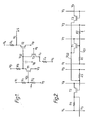
- the circuit diagram represents the circuitry interposed between a photosensitive reading element in the form of a photoresistor R2 and a marking element in the form of a stylus S.
- the circuit represents only one section of the image bar; it is repeated as many times as there are photosensors and styli in the image bar, for example of the order of 3000 of them to cover an A4 page width.
- the circuit of Figure 1 includes three transistors T 1 , T 2 and T 3 , and four resistors R 1 to R 4 .
- the two-stage amplifier incorporating transistors T 1 and T 2 is used, the first stage (T 1 ) being a low-voltage high gain stage, and the second stage (T 2 ) being a high-voltage but relatively low gain stage.
- V 1 and V 3 set at a fixed low voltage V LT
- V 22 V 5' V 7 and V 8 set at zero volts
- V 4 set at a relatively high voltage V HT .
- V G1 at the base of transistor T 1 is substantially VLT since the resistance of R 2 is high. If light falls on the photoresistor R 2 due to a reading from a white portion of the original, the resistance of photoresistor R 2 decreases, and V G1 falls to substantially zero.
- V Gl With V Gl at V LT (black original), the voltage V G2 at the output of transistor T 1 is substantially zero, so the transistor T 2 is non-conductive, and a voltage of substantially V HT (as applied at V4) appears at the stylus S.
- V G1 at zero white original
- the voltage V G2 at the output of transistor T 1 is substantially V LT , and transistor T 2 becomes conductive. This lowers the voltage of the stylus to substantially zero, so no output mark is made.
- the circuit of Fig 1 enables information from an image bar at a remote location to be read out, as well as enabling information to be sent to a remote image bar.
- These read-out and write-in capabilities may be used alone, or in combination with copying, thereby allowing electronic forms overlay techniques to be used, as well as editing.
- Interfacing between image bar circuits is achieved by way of transistor T 3 , which acts as a bidirectional series gate.
- the mode of operation of the circuit of Figure 1 is determined by the set of voltages V 1 to V 6 .
- the following table shows the operating conditions for the circuit. V 7 and V 8 are at zero volts throughout. In the read-out mode, output information appears at V 0 , and in the write-in mode, data is input at V 6 .
- Figures 2, 3 and 4 one way of putting the invention into effect is illustrated.
- Figure 2 shows the circuit elements of Figure 1 re-arranged to correspond physically with the layout of Figs 3 and 4.
- the circuit elements including thin film transistors T 1 , T 2 and T 3 , are deposited by thin film techniques on a substrate, such as a glass substrate, and a succession of circuits are laid out side by side with common lines for fixed voltages V 1 to V 5 and V 7 and V a running transversely through all the circuits as best seen in Figure 4.
- Each circuit has its own stylus output line (for voltage Vs), its own interfacing line (for voltage V 0 ) , and its own photoresistor R 2 .
- the photoresistor R 2 of each circuit is illuminated from below through the glass substrate.
- Neighbouring components eg transistors T 1 and T 3
- the amplifiers drive all the styli in parallel and can therefore present a continuous drive at the stylus nibs.
- the styli do not, therefore, need plating for either the breakdown or contact methods of charging.
- a storage capacitor can be provided easily within the amplifier by lengthening the bar at X-X in Figure 3 where the V G2 line runs beneath the V 8 line.
- Thin film transistor T 3 acts as bidirectional series gate, and the load impedances Z o provide bias from V 6 .
- a logical "OR" gate function occurs on each data line V 0 .
- V 5 the voltage which is the amplified photosensor signal for that circuit element.
- the transistors T 3 are biassed into conduction by suitable drivers connected to the V 5 lines.
- the information on a V 0 line is buffered via a buffer 10, into a register 11 in the shift register element 12 of the peripheral logic circuit, and sets the data input of the shift register. Data is loaded into the register by enabling parallel entry, and the video signals are shifted out by normal serial operation of the register.
- the stylus drive transistor T 2 can be addressed via transistor T 3 .
- Transistor T 2 follows an electronic signal provided by shift register latch 13. This is accomplished by selecting the appropriate series gate element (transistor T 3 ) and enabling the low impedance state of a tri-state buffer 14. Parallel entry to the shift register is disabled during this mode, and the photosensor circuit is also disabled by switching V 1 to the low state.
- the image bar may also be used in modes which combine copying with either writing or reading.
- Combining copying with writing allows electronic forms overlay and editing functions.
- Combining copying with reading allows output monitoring, giving a copy of transmitted documents. Harnessing several machines together allows simultaneous multiple copying with collation.
- the image bar 20 comprises a glass substrate 21 which carries the thin film circuits 22.
- the stylus nibs 23 of the styli S are at the lower extremity of the thin film circuits 22.
- the glass substrate 21 and the thin film circuits 22 are encased in a potting material 24.
- a card 25 for peripheral circuits is secured to the potting material by means of card supports 26.
- the peripheral circuitry may be included, for example, in a forty-pin integrated circuit chip 27, with connections to the thin film circuits 22 being made by way of a flexi-connector 28.
- the photoresistors R 2 are located just above the styli S, and a line image of a document 29 being copied is formed along the line of photoresistors.
- Document 29 is supported on a platen 30 and is illuminated by a light source (not shown).
- a strip lens 31 forms the required line image on photoresistors R 2 by way of a plane mirror 32. In order to form a complete image of the document being copied, relative movement takes place between the document and the image bar.
- the electrical impulses supplied to stylus nibs 23 are used to form an image on an imaging sheet 33 which is passed under the nibs in contact with them and at the appropriate speed proportional to the speed of relative movement between the document and the image bar.
- Any suitable form of recording may be used.
- the imaging sheet 33 may record an image directly, by coloration of the sheet due to the action of the electrical impulses supplied by the stylus nibs, or it may record an eletrostatic latent image (on a dielectric-surfaced sheet) for subsequent development by standard electrographic techniques.
- electrochromic marking techniques may be used, or the outputs may be used to operate ink jets instead of the styli described above.
Abstract
Description
- This invention relates to an imaging device which includes an array of photosensitive reading elements and a set of associated marking elements, one for each reading element. An electrical circuit is interposed between each reading element and its associated marking element, and all of the reading elements, marking elements, and circuits are carried by a common structure.
- Such an imaging device may consist of a linear array of photosensors, such as photoresistors, coupled electrically to a parallel array of marking elements such as styli. All of the sets of photosensors and styli (and their associated coupling circuits) operate individually, simultaneously, and in parallel. A device of this kind, which may be called an image bar, may be used as a copier element by exposing the photosensor array to an illuminated line image of an original, and scanning either the image or the image bar to give a line-by-line scan of the original. The output side of the image bar simultaneously writes a line-by-line charge image on to a suitable receptor to either cause direct colouration in correspondence with the original or to provide a latent image for subsequent development.
- An image bar of this general kind used as a copier element is described in US Patent Specification No 3409899.
- If the known kind of image bar is used with known photosensitive materials, the levels of illumination required for practical copying purposes are very much larger than those required by conventional copiers.
- The present invention seeks to overcome this excessive illumination requirement by providing an image bar which is characterised in that each of the electrical circuits (interposed between the reading elements and their associated marking elements) includes an amplifier. Particularly useful circuit elements for such an amplifier are thin film transistors.
- The advantages offered by the invention are that by providing the amplifiers on the common structure, the low cost and compact nature of the image bar are maintained. The use of thin film transistor amplifiers allows the fabrication of the photosensors, amplifiers and styli in a compatible technology, giving rise to a low cost unit with sufficient amplification that the illumination requirement can be reduced below that of a conventional copier. This enables the design of a very low cost, low power, portable copier.
- Ways of putting the invention into effect will now be described in more detail, with reference to the accompanying drawings, in which:-
- Figure 1 is a circuit diagram of one section (reading element, electrical circuit, marking element) of an image bar in accordance with the invention, including an interface arrangement for communication with a remote image bar;
- Figures 2, 3 and 4 are respectively an equivalent circuit, a side view, and a plan view of one possible construction of the image bar whose circuit is shown in Figure 1;
- Figure 5 is a schematic diagram of an input-output arrangement for the image bar of Figures 1 to 4;
- Figure 6 is a side view of the image bar arranged for copying a document.
- Referring to Figure 1, the circuit diagram represents the circuitry interposed between a photosensitive reading element in the form of a photoresistor R2 and a marking element in the form of a stylus S. The circuit represents only one section of the image bar; it is repeated as many times as there are photosensors and styli in the image bar, for example of the order of 3000 of them to cover an A4 page width.
- The circuit of Figure 1 includes three transistors T1, T2 and T3, and four resistors R1 to R4. For use of the image bar in the direct copying mode, the two-stage amplifier incorporating transistors T1 and T2 is used, the first stage (T1) being a low-voltage high gain stage, and the second stage (T2) being a high-voltage but relatively low gain stage. With V1 and V3 set at a fixed low voltage VLT, with V 22 V5' V7 and V8 set at zero volts, and with V4 set at a relatively high voltage VHT, the. circuit is ready for direct copying. If no light falls on photoresistor R2, due to a reading from a black portion of the original to be copied, then the voltage VG1 at the base of transistor T1 is substantially VLT since the resistance of R 2 is high. If light falls on the photoresistor R2 due to a reading from a white portion of the original, the resistance of photoresistor R2 decreases, and VG1 falls to substantially zero.
- With VGl at VLT (black original), the voltage VG2 at the output of transistor T1 is substantially zero, so the transistor T2 is non-conductive, and a voltage of substantially VHT (as applied at V4) appears at the stylus S. With VG1 at zero (white original), the voltage VG2 at the output of transistor T1 is substantially VLT, and transistor T2 becomes conductive. This lowers the voltage of the stylus to substantially zero, so no output mark is made.
- In addition to providing a direct copying capability, the circuit of Fig 1 enables information from an image bar at a remote location to be read out, as well as enabling information to be sent to a remote image bar. These read-out and write-in capabilities may be used alone, or in combination with copying, thereby allowing electronic forms overlay techniques to be used, as well as editing. Interfacing between image bar circuits is achieved by way of transistor T3, which acts as a bidirectional series gate.
- The mode of operation of the circuit of Figure 1 is determined by the set of voltages V1 to V6. The following table shows the operating conditions for the circuit. V7 and V8 are at zero volts throughout. In the read-out mode, output information appears at V0, and in the write-in mode, data is input at V6.

- Since only short pulses are normally involved, a storage capacitor can be provided easily within the amplifier by lengthening the bar at X-X in Figure 3 where the VG2 line runs beneath the V8 line.
- Suitable electronic interfacing for utilisingtheread-out and write-in capabilities of the image bar is shown in figure 5. Thin film transistor T3 acts as bidirectional series gate, and the load impedances Zo provide bias from V6.
- In the read-out mode, ie, when the image bar is being used to read a document and send the information to, for example, another (remote) image bar, a logical "OR" gate function occurs on each data line V0. When a transistor T3 is biassed into conduction (V5 high) the associated data line V0 follows the voltage VG2 which is the amplified photosensor signal for that circuit element. The transistors T 3 are biassed into conduction by suitable drivers connected to the V 5 lines. The information on a V0 line is buffered via a
buffer 10, into aregister 11 in theshift register element 12 of the peripheral logic circuit, and sets the data input of the shift register. Data is loaded into the register by enabling parallel entry, and the video signals are shifted out by normal serial operation of the register. - In the write-in mode, ie, when the image bar is being used to write information received from, for example, another (remote) image bar, the stylus drive transistor T2 can be addressed via transistor T3. Transistor T2 follows an electronic signal provided by
shift register latch 13. This is accomplished by selecting the appropriate series gate element (transistor T3) and enabling the low impedance state of a tri-statebuffer 14. Parallel entry to the shift register is disabled during this mode, and the photosensor circuit is also disabled by switching V1 to the low state. - As already mentioned, the image bar may also be used in modes which combine copying with either writing or reading. Combining copying with writing allows electronic forms overlay and editing functions. Combining copying with reading allows output monitoring, giving a copy of transmitted documents. Harnessing several machines together allows simultaneous multiple copying with collation.
- An example of an arrangement incorporating the layout of figures 2-5 is shown in figure 6. The
image bar 20 comprises aglass substrate 21 which carries thethin film circuits 22. Thestylus nibs 23 of the styli S are at the lower extremity of thethin film circuits 22. Theglass substrate 21 and thethin film circuits 22 are encased in apotting material 24. Acard 25 for peripheral circuits is secured to the potting material by means of card supports 26. The peripheral circuitry may be included, for example, in a forty-pin integratedcircuit chip 27, with connections to thethin film circuits 22 being made by way of a flexi-connector 28. - The photoresistors R2 are located just above the styli S, and a line image of a
document 29 being copied is formed along the line of photoresistors.Document 29 is supported on aplaten 30 and is illuminated by a light source (not shown). Astrip lens 31 forms the required line image on photoresistors R2 by way of aplane mirror 32. In order to form a complete image of the document being copied, relative movement takes place between the document and the image bar. - The electrical impulses supplied to
stylus nibs 23 are used to form an image on animaging sheet 33 which is passed under the nibs in contact with them and at the appropriate speed proportional to the speed of relative movement between the document and the image bar. Any suitable form of recording may be used. Thus, theimaging sheet 33 may record an image directly, by coloration of the sheet due to the action of the electrical impulses supplied by the stylus nibs, or it may record an eletrostatic latent image (on a dielectric-surfaced sheet) for subsequent development by standard electrographic techniques. Alternatively, electrochromic marking techniques may be used, or the outputs may be used to operate ink jets instead of the styli described above.
Claims (7)
Applications Claiming Priority (2)
| Application Number | Priority Date | Filing Date | Title |
|---|---|---|---|
| GB8125080 | 1981-08-11 | ||
| GB8125080 | 1981-08-17 |
Publications (3)
| Publication Number | Publication Date |
|---|---|
| EP0074719A2 true EP0074719A2 (en) | 1983-03-23 |
| EP0074719A3 EP0074719A3 (en) | 1983-06-15 |
| EP0074719B1 EP0074719B1 (en) | 1986-03-12 |
Family
ID=10523986
Family Applications (1)
| Application Number | Title | Priority Date | Filing Date |
|---|---|---|---|
| EP82304252A Expired EP0074719B1 (en) | 1981-08-11 | 1982-08-11 | Imaging device |
Country Status (5)
| Country | Link |
|---|---|
| US (1) | US4466020A (en) |
| EP (1) | EP0074719B1 (en) |
| JP (1) | JPS5839165A (en) |
| CA (1) | CA1192603A (en) |
| DE (1) | DE3269826D1 (en) |
Cited By (4)
| Publication number | Priority date | Publication date | Assignee | Title |
|---|---|---|---|---|
| EP0263602A2 (en) * | 1986-09-11 | 1988-04-13 | Xerox Corporation | Multifunction fluid jet-assisted ion projection marking head |
| GB2222114A (en) * | 1988-08-12 | 1990-02-28 | Scient Generics Ltd | Improvements relating to bar code printing |
| GB2223454A (en) * | 1988-08-12 | 1990-04-11 | Scient Generics Ltd | Printers and ancillary systems |
| EP0917341A1 (en) * | 1996-07-30 | 1999-05-19 | Rohm Co., Ltd. | Picture reading/writing head and integrated circuit used for the same |
Families Citing this family (16)
| Publication number | Priority date | Publication date | Assignee | Title |
|---|---|---|---|---|
| US4706128A (en) * | 1983-12-14 | 1987-11-10 | Canon Kabushiki Kaisha | Image reading and converting apparatus |
| US4766450A (en) * | 1987-07-17 | 1988-08-23 | Xerox Corporation | Charging deposition control in electrographic thin film writting head |
| JP2717249B2 (en) * | 1987-12-29 | 1998-02-18 | セイコーインスツルメンツ株式会社 | Image reading and printing device |
| US4977416A (en) * | 1989-09-21 | 1990-12-11 | Rastergraphics, Inc. | Integrated thick film electrostatic writing head |
| US5040074A (en) * | 1990-05-02 | 1991-08-13 | Xerox Corporation | Full-width simultaneous read/write copier |
| US5162916A (en) * | 1990-07-02 | 1992-11-10 | Xerox Corporation | Compact read/write scanner |
| JPH04233863A (en) * | 1990-12-28 | 1992-08-21 | Rohm Co Ltd | Image sensor |
| US5237346A (en) * | 1992-04-20 | 1993-08-17 | Xerox Corporation | Integrated thin film transistor electrographic writing head |
| US5166960A (en) * | 1992-04-20 | 1992-11-24 | Xerox Corporation | Parallel multi-phased a-Si shift register for fast addressing of an a-Si array |
| US5491566A (en) * | 1992-11-27 | 1996-02-13 | Goldstar Co., Ltd. | Integrated input-output device having a reading and a printing section on a single substrate |
| US5337080A (en) * | 1993-04-27 | 1994-08-09 | Xerox Corporation | Amorphous silicon electrographic writing head assembly with protective cover |
| US5991055A (en) * | 1996-09-23 | 1999-11-23 | Hewlett-Packard Company | Underpulsed scanner with variable scan speed, P. W. M. color balance, scan modes and column reversal |
| US6864999B1 (en) | 1998-07-13 | 2005-03-08 | Rohm Co., Ltd. | Integrated image-reading/writing head and image processing apparatus incorporating the same |
| US6947184B1 (en) * | 1998-11-09 | 2005-09-20 | Rohm Co., Ltd. | Integral image readin/writing head, image processor provided with this, image reading head and print head |
| WO2005031636A1 (en) * | 2003-09-24 | 2005-04-07 | Authentec, Inc. | Finger biometric sensor with sensor electronics distributed over thin film and monocrystalline substrates and related methods |
| EP3633258A1 (en) | 2018-10-04 | 2020-04-08 | Raccorderie Metalliche S.p.A. | Quick-connect pipe fitting |
Citations (5)
| Publication number | Priority date | Publication date | Assignee | Title |
|---|---|---|---|---|
| US3409899A (en) * | 1964-09-01 | 1968-11-05 | Eastman Kodak Co | Photoresponsive electrostatic image recording apparatus with charging electrode matrix array |
| US3512158A (en) * | 1968-05-02 | 1970-05-12 | Bunker Ramo | Infra-red printer |
| US3953681A (en) * | 1973-07-04 | 1976-04-27 | U.S. Philips Corporation | Combined recording and scanning device for facsimile transmission |
| US4041519A (en) * | 1975-02-10 | 1977-08-09 | Melen Roger D | Low transient effect switching device and method |
| AT368321B (en) * | 1976-09-15 | 1982-10-11 | Siemens Ag | SEMICONDUCTOR DIODE DEVICE, ESPECIALLY SEMICONDUCTOR DIODE ROW, FOR GENERATING OR RECEIVING RADIATION |
Family Cites Families (6)
| Publication number | Priority date | Publication date | Assignee | Title |
|---|---|---|---|---|
| US3205302A (en) * | 1962-11-02 | 1965-09-07 | Ibm | Facsimile transmission system |
| US3318996A (en) * | 1963-08-12 | 1967-05-09 | Inst Scient Information | Document copying device having parallel signal transmission parts |
| JPS5479511A (en) * | 1977-12-08 | 1979-06-25 | Fuji Xerox Co Ltd | Scan reader |
| JPS54152419A (en) * | 1978-05-22 | 1979-11-30 | Ricoh Co Ltd | Facsimile equipment |
| US4257071A (en) * | 1979-07-09 | 1981-03-17 | Lamb Reginald T | Apparatus for digitizing optical images |
| JPS5639675A (en) * | 1979-09-06 | 1981-04-15 | Ricoh Co Ltd | Facsimile equipment and its head |
-
1982
- 1982-08-11 EP EP82304252A patent/EP0074719B1/en not_active Expired
- 1982-08-11 DE DE8282304252T patent/DE3269826D1/en not_active Expired
- 1982-08-13 JP JP57140905A patent/JPS5839165A/en active Granted
- 1982-08-16 CA CA000409523A patent/CA1192603A/en not_active Expired
- 1982-08-16 US US06/408,110 patent/US4466020A/en not_active Expired - Fee Related
Patent Citations (5)
| Publication number | Priority date | Publication date | Assignee | Title |
|---|---|---|---|---|
| US3409899A (en) * | 1964-09-01 | 1968-11-05 | Eastman Kodak Co | Photoresponsive electrostatic image recording apparatus with charging electrode matrix array |
| US3512158A (en) * | 1968-05-02 | 1970-05-12 | Bunker Ramo | Infra-red printer |
| US3953681A (en) * | 1973-07-04 | 1976-04-27 | U.S. Philips Corporation | Combined recording and scanning device for facsimile transmission |
| US4041519A (en) * | 1975-02-10 | 1977-08-09 | Melen Roger D | Low transient effect switching device and method |
| AT368321B (en) * | 1976-09-15 | 1982-10-11 | Siemens Ag | SEMICONDUCTOR DIODE DEVICE, ESPECIALLY SEMICONDUCTOR DIODE ROW, FOR GENERATING OR RECEIVING RADIATION |
Cited By (8)
| Publication number | Priority date | Publication date | Assignee | Title |
|---|---|---|---|---|
| EP0263602A2 (en) * | 1986-09-11 | 1988-04-13 | Xerox Corporation | Multifunction fluid jet-assisted ion projection marking head |
| EP0263602A3 (en) * | 1986-09-11 | 1989-03-22 | Xerox Corporation | Multifunction fluid jet-assisted ion projection marking head |
| GB2222114A (en) * | 1988-08-12 | 1990-02-28 | Scient Generics Ltd | Improvements relating to bar code printing |
| GB2223454A (en) * | 1988-08-12 | 1990-04-11 | Scient Generics Ltd | Printers and ancillary systems |
| US5149211A (en) * | 1988-08-12 | 1992-09-22 | Pettigrew Robert M | Printers and ancillary systems |
| EP0917341A1 (en) * | 1996-07-30 | 1999-05-19 | Rohm Co., Ltd. | Picture reading/writing head and integrated circuit used for the same |
| EP0917341A4 (en) * | 1996-07-30 | 1999-07-14 | Rohm Co Ltd | Picture reading/writing head and integrated circuit used for the same |
| US6222581B1 (en) | 1996-07-30 | 2001-04-24 | Rohm Co., Ltd. | Picture reading/writing head and integrated circuit used for the same |
Also Published As
| Publication number | Publication date |
|---|---|
| CA1192603A (en) | 1985-08-27 |
| EP0074719A3 (en) | 1983-06-15 |
| JPH0586104B2 (en) | 1993-12-09 |
| US4466020A (en) | 1984-08-14 |
| EP0074719B1 (en) | 1986-03-12 |
| DE3269826D1 (en) | 1986-04-17 |
| JPS5839165A (en) | 1983-03-07 |
Similar Documents
| Publication | Publication Date | Title |
|---|---|---|
| EP0074719B1 (en) | Imaging device | |
| EP0441541B1 (en) | Photoelectric converting device | |
| US7528625B2 (en) | Image forming apparatus | |
| JP2991354B2 (en) | Picture reader and picture information processing unit having the same | |
| US4549223A (en) | Reading, printing and copying device | |
| US4737805A (en) | Multifunction ionographic marking apparatus | |
| CA1203835A (en) | Read/write bar for multi-mode reproduction machine | |
| US5162644A (en) | Contact type image sensor having photoelectric conversion elements to reduce signal variation caused by luminous intensity variation of light source | |
| US4347533A (en) | Facsimile reading and recording device | |
| EP0294833B1 (en) | Contact photoelectric conversion device | |
| TW391928B (en) | Recording head and image forming apparatus using the same | |
| KR100359638B1 (en) | Image processor | |
| EP0297413A2 (en) | Photoelectric conversion device | |
| JPS5829266A (en) | Copying machine | |
| US4797571A (en) | Contact type image sensor | |
| US5138467A (en) | Photoelectric conversion device | |
| JPS5880865A (en) | Original read-out device | |
| JPS60244062A (en) | Photosensor | |
| EP0013161A1 (en) | Apparatus for reproducing graphic information | |
| JP2023034507A (en) | Semiconductor device, image reading device, and method for controlling semiconductor device | |
| JPS61284169A (en) | Recorder | |
| JP2591346B2 (en) | Image reading device | |
| JPH0645578A (en) | Thin film image sensor | |
| JPS58157252A (en) | Picture reader serving also as light source for picture formation | |
| JPH02219268A (en) | Semiconductor device and photoelectric converter using same |
Legal Events
| Date | Code | Title | Description |
|---|---|---|---|
| PUAI | Public reference made under article 153(3) epc to a published international application that has entered the european phase |
Free format text: ORIGINAL CODE: 0009012 |
|
| AK | Designated contracting states |
Designated state(s): DE FR GB NL |
|
| PUAL | Search report despatched |
Free format text: ORIGINAL CODE: 0009013 |
|
| AK | Designated contracting states |
Designated state(s): DE FR GB NL |
|
| 17P | Request for examination filed |
Effective date: 19831103 |
|
| GRAA | (expected) grant |
Free format text: ORIGINAL CODE: 0009210 |
|
| AK | Designated contracting states |
Kind code of ref document: B1 Designated state(s): DE FR GB NL |
|
| REF | Corresponds to: |
Ref document number: 3269826 Country of ref document: DE Date of ref document: 19860417 |
|
| ET | Fr: translation filed | ||
| PLBE | No opposition filed within time limit |
Free format text: ORIGINAL CODE: 0009261 |
|
| STAA | Information on the status of an ep patent application or granted ep patent |
Free format text: STATUS: NO OPPOSITION FILED WITHIN TIME LIMIT |
|
| 26N | No opposition filed | ||
| PGFP | Annual fee paid to national office [announced via postgrant information from national office to epo] |
Ref country code: GB Payment date: 19950731 Year of fee payment: 14 |
|
| PGFP | Annual fee paid to national office [announced via postgrant information from national office to epo] |
Ref country code: FR Payment date: 19950809 Year of fee payment: 14 Ref country code: DE Payment date: 19950809 Year of fee payment: 14 |
|
| PG25 | Lapsed in a contracting state [announced via postgrant information from national office to epo] |
Ref country code: GB Effective date: 19960811 |
|
| PGFP | Annual fee paid to national office [announced via postgrant information from national office to epo] |
Ref country code: NL Payment date: 19960831 Year of fee payment: 15 |
|
| GBPC | Gb: european patent ceased through non-payment of renewal fee |
Effective date: 19960811 |
|
| PG25 | Lapsed in a contracting state [announced via postgrant information from national office to epo] |
Ref country code: FR Effective date: 19970430 |
|
| PG25 | Lapsed in a contracting state [announced via postgrant information from national office to epo] |
Ref country code: DE Effective date: 19970501 |
|
| REG | Reference to a national code |
Ref country code: FR Ref legal event code: ST |
|
| PG25 | Lapsed in a contracting state [announced via postgrant information from national office to epo] |
Ref country code: NL Free format text: LAPSE BECAUSE OF NON-PAYMENT OF DUE FEES Effective date: 19980301 |
|
| NLV4 | Nl: lapsed or anulled due to non-payment of the annual fee |
Effective date: 19980301 |