EP0075673A1 - A method of retrieving character symbol data elements for a display and apparatus therefore - Google Patents
A method of retrieving character symbol data elements for a display and apparatus therefore Download PDFInfo
- Publication number
- EP0075673A1 EP0075673A1 EP82106660A EP82106660A EP0075673A1 EP 0075673 A1 EP0075673 A1 EP 0075673A1 EP 82106660 A EP82106660 A EP 82106660A EP 82106660 A EP82106660 A EP 82106660A EP 0075673 A1 EP0075673 A1 EP 0075673A1
- Authority
- EP
- European Patent Office
- Prior art keywords
- bits
- display
- memory
- compare
- character code
- Prior art date
- Legal status (The legal status is an assumption and is not a legal conclusion. Google has not performed a legal analysis and makes no representation as to the accuracy of the status listed.)
- Granted
Links
Images


Classifications
-
- G—PHYSICS
- G09—EDUCATION; CRYPTOGRAPHY; DISPLAY; ADVERTISING; SEALS
- G09G—ARRANGEMENTS OR CIRCUITS FOR CONTROL OF INDICATING DEVICES USING STATIC MEANS TO PRESENT VARIABLE INFORMATION
- G09G5/00—Control arrangements or circuits for visual indicators common to cathode-ray tube indicators and other visual indicators
- G09G5/22—Control arrangements or circuits for visual indicators common to cathode-ray tube indicators and other visual indicators characterised by the display of characters or indicia using display control signals derived from coded signals representing the characters or indicia, e.g. with a character-code memory
- G09G5/24—Generation of individual character patterns
-
- G—PHYSICS
- G09—EDUCATION; CRYPTOGRAPHY; DISPLAY; ADVERTISING; SEALS
- G09G—ARRANGEMENTS OR CIRCUITS FOR CONTROL OF INDICATING DEVICES USING STATIC MEANS TO PRESENT VARIABLE INFORMATION
- G09G1/00—Control arrangements or circuits, of interest only in connection with cathode-ray tube indicators; General aspects or details, e.g. selection emphasis on particular characters, dashed line or dotted line generation; Preprocessing of data
- G09G1/02—Storage circuits
Definitions
- the present invention relates to character generators for apparatus for displaying information and more particularly, but not exclusively, to a keyboard terminal controlled display in which the characters displayed are in the form of dot patterns selected from a character memory which receives address information from a keyboard or computer identifying the character to be displayed. Part or all of the dot pattern of the character to be displayed is provided at the output of the character memory.
- the character memory is embodied in the form of a read only memory integrated circuit module which can be replaced by different read only memory modules to display the different character sets of different languages. More recently, characters of several languages have been provided in a single character memory and characters common to one or more languages are shared by the languages to avoid the need for duplicating common characters.
- One such character generating system is disclosed in US-A-4,122,533, and includes a multiplexor and a plurality of language symbol selecting programmable read only memories between a refresh buffer 40 and a character generator read only memory. The use of translating or directory memories between the refresh buffer and the character generator presents a significant cost and level of complexity.
- the present invention provides an improved method and apparatus for addressing a character generator memory wherein symbols common to two or more languages are provided in a common area of the character generator memory in order to memorize the total character generator memory required for all symbols of a plurality of languages. Symbols which are special to the particular language being displayed are stored in one of a plurality of special symbol areas of the character generator memory. One of the special symbol areas contiguous with the common area is identified as a default symbol area. The proper special symbol area of the character generator memory is selected by comparing the high order bits of a display character code with compare bits to determine whether a different special symbol area of the character generator memory is to be substituted for the default area contiguous with the common area. If the compare bits indicate that a different special area of the character generator is to be substituted, the high order bits of the display character code are not directly used to address the character generator memory but are replaced by substitution bits to access that special symbol area unique to the language being displayed.
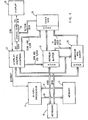
- a keyboard display ( Figure 1) incorporating the invention is controlled by a microprocessor 11 and a program in memory 13.
- Keyboard scan codes are received from keyboard 15 on the data bus 17 and translated into codes for storage and display.
- the data can be translated into ASCII or EBCDIC.
- the input codes can be stored in memory 13 and transferred to refresh buffer 21.
- Refresh buffer 21 and registers in compare and substitution logic circuit 25 may be memory mapped into the addressable memory space of microprocessor 11. From refresh buffer 21, characters to be displayed are used as part of the address to access character generator read only memory 23.
- the high order bits of each display character code stored in refresh buffer 21 are sent to compare and substitution logic circuit 25 for comparison with bits stored in the compare register.
- substitution bits stored in the substitution register are sent to the high order address inputs of read only storage in character generator 23.
- the low order bits of each display character code stored in refresh buffer 21 are used directly as intermediate address bits to character generator 23.
- the low order address bit inputs to character generator 23 are provided by a scan line clock output from display control counters 27.
- Display control counters 27 also generate a bit clock, and a row and column clock. Each of these clocks is provided by an output from one or more counters which provide a digital time base operating in synchronism with the display, in this embodiment a cathode ray tube.
- the display control counters remain in sync because the display periodically provides a sync pulse to the display control counters.
- the row and column clock is supplied to the address input of refresh buffer 21.
- the rpw and column clock controls access to refresh buffer 21 storage locations while refreshing the cathode ray tube display.
- the character codes from refresh buffer 21 are provided on its data output and form part of the address to the character generator.
- the scan line clock provides the remaining or low order address bits. For any scan line, the scan line clock remains at a particular count while the refresh buffer provides a different character code for each column.
- the character generator 23 provides a byte of pattern data to serializer 29 for each character column of each display raster scan line.
- the byte of data in serializer 29 is then shifted to the display as picture element data by the picture element clock.
- connections are provided via address bus 19 and data bus 17 to microprocessor 11 for loading the compare and substitution registers.
- the registers in logic circuit 25 are also memory mapped into the address space of microprocessor 11, so that microprocessor 11 can load values into the compare and substitution registers in the same manner as it stores a byte in any other memory location.
- the compare and subsitution registers are connected to the output of the refresh buffer rather than the output of microprocessor 11. Connection to the output of refresh buffer 21 permits the compare and substitution registers to be loaded by display control orders rather than the microprocessor 11. Providing the ability to load the compare and subsitution registers from the refresh buffer permits each field of display data to be preceded by a display order which controls the language of the field on a field-by- field basis.
- This alternative embodiment is described in more detail with respect to Figure 4.
- two high order address bits of each eight bit display character code can be converted into three high order address bits to access a particular section of character generator 23 to display a particular language without the need for directory memories or physically changing the character generator memory.
- refresh buffer 21 and character generator 23 are shown in combination with the compare and substitution logic circuit in greater detail.
- the compare register and the substitution register are combined into one 8-bit register 111. Only the first five bits of this eight bit register are used for the invention in this limited embodiment. The first two bit positions, namely bit 0 and bit 1, store the compare bits, and the next three bit positions, namely bits 2, 3 and 4, store the substitution bits. In this way, a single byte command or display order can change the language of the display.
- each character code output provided by refresh buffer 21 provides the remainder of the address.
- Character code bits 0 to 5 of each character code are used directly to provide address inputs to lines A4 to A9 to character generator 23.
- Bits 6 and 7 of each display character code are provided to the compare and substitution logic circuit which generates address inputs for lines A10, All and A12.
- the compare means of the invention is embodied in exclusive OR invert circuits 113 and 115 having outputs connected to AND gate 117.
- Exclusive OR invert gate 113 has inputs connected to the display character code bit 6 and to the compare register bit 0.
- Exclusive OR invert gate 113 has inputs connected to display character code bit 6 and to the compare register bit 0.
- Exclusive OR invert gate 115 has inputs connected to the display character code bit 7 and the compare register bit 1.
- the output of AND gate 117 is inverted by inverter 119 to condition AND gates 121 and 123 whose other inputs are the bits 6 and 7 from refresh buffer 21.
- AND gates 121 and 123 then provide bits 6 and 7 to address lines A10 and All to access a display character stored in the common area of the memory of character generator 23.
- bits 6 and 7 of the display character code are the same as the bits stored in compare bits 0 and 1 of register lll
- the output of AND gate 117 is supplied to AND gates 127, 129 and 131 whose other inputs are the substitution bits 2, 3 and 4, so that the AND gates 127, 129 and 131 transfer the
- OR gates 133 and 135 connect AND gates 121, 127 and 123, 129 to address input lines A10 and All respectively to provide these address inputs under both compare and noncompare conditions.
- the output of AND gate 131 can be connected directly to the address input A12 because in the instant embodiment, the common area of the memory of character generator 23 is in the first half of the memory and therefore the bit on the A12 line is a zero when this area is accessed.
- the Al2 address line will only be a logical one when special symbol areas of the memory are being accessed. Accordingly, a noncompare condition provided by the compare logic circuit causes gate 131 to provide a logical zero to address line Al2 effectively accessing the common area of the memory of character generator 23.
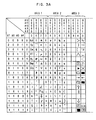
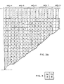
- Figure 3 shows a sample placement of character patterns in the memory of character generator 23.
- the lowest order address lines AO to A3 are not shown in Figure 3 because the patterns themselves are not shown at the picture element level. Rather, symbolic images of the characters are shown at the intersection of rows and columns having corresponding bit patterns which would access the first slice of pattern data of the selected character.
- Address bit pattern combinations for address lines A4 to A7 are shown down the lefthand side of Figure 3 while address bit combinations for address lines A8 to A12 are shown across the top of Figure 3.
- Address bit pattern combination in address lines A10, All and A12 controls selection of one of the areas 1 to 8 of the memory.
- address line Al2 is a logical zero for the common and default areas of the memory. Therefore areas 1 to 4 include the common and default areas.
- the default area can be any one of areas 1 to 4 as defined by the bits stored in compare bit positions 0 and 1 of register lll. If register 111 contains all zeros, area 1 will be the default area. Even though bits 6 and 7 are the same as bits 0 and 1 of register 111 causing substitution, the default area is substituted for itself. If bit positions 0 and 1 contain ones and bit positions 2, 3 and 4 contain a binary 110, area 4 becomes the default area.
- substitution bit position 4 of register 111 must be loaded with a binary 1.
- area 5 containing the special symbols unique to Katakana and Japanese English will be accessible in combination with areas 1, 2 and 3 containing the Latin alphabet and control symbols common to both English and Japanese English.
- bit pattern 11101 will select area 6 in combination with areas 1, 2 and 3 to display languages using the Latin alphabets plus special Hebrew characters.
- a bit pattern of 11101 in register 111 will give access to areas 1, 2, 3 and 7 of the memory of character generator 23 to display information in languages using the Latin alphabets plus Greek, Yugoslav, and Turkish language information.
- area 5, 6 or 7 were substituted for default area 4 which includes symbols special to Icelandic, Hungarian and viteans.
- all eight display character code output bits are provided to a plurality of control logic gates for loading register 111.
- Bits 7, 6 and 5 are provided to AND gate 151, bits 6 and 5 being inverted by inverters 153 and 155.
- AND gate 151 identifies the first two columns of area 3 shown in Figure 3 as containing blanks, that is, no displayable symbol patterns appear at these locations. Instead, these display character codes can be used as display orders for loading register 111.
- display character code bits 4, 3, 2, 1 and 0 are gated directly through AND gates 157, 159, 161, 163, 165 by the output of AND gate 151 into corresponding storage positions of register 111.
- the embodiment of Figure 4 avoids the need for the processor to load the register 111 directly and permits display orders controlling the loading of register 111 to be embedded in the display character code stream. In this way, fields being displayed can each be easily displayed in a different language.
Abstract
Description
- The present invention relates to character generators for apparatus for displaying information and more particularly, but not exclusively, to a keyboard terminal controlled display in which the characters displayed are in the form of dot patterns selected from a character memory which receives address information from a keyboard or computer identifying the character to be displayed. Part or all of the dot pattern of the character to be displayed is provided at the output of the character memory.
- Often, the character memory is embodied in the form of a read only memory integrated circuit module which can be replaced by different read only memory modules to display the different character sets of different languages. More recently, characters of several languages have been provided in a single character memory and characters common to one or more languages are shared by the languages to avoid the need for duplicating common characters. One such character generating system is disclosed in US-A-4,122,533, and includes a multiplexor and a plurality of language symbol selecting programmable read only memories between a refresh buffer 40 and a character generator read only memory. The use of translating or directory memories between the refresh buffer and the character generator presents a significant cost and level of complexity. It is also known that a limited address field can be used with a register of extra bits to access a memory larger than could be defined by the address field alone. The prior art proposals, as exemplified in US-A-4,057,848, are complex and expensive however and not suited for use in a display.
- The present invention provides an improved method and apparatus for addressing a character generator memory wherein symbols common to two or more languages are provided in a common area of the character generator memory in order to memorize the total character generator memory required for all symbols of a plurality of languages. Symbols which are special to the particular language being displayed are stored in one of a plurality of special symbol areas of the character generator memory. One of the special symbol areas contiguous with the common area is identified as a default symbol area. The proper special symbol area of the character generator memory is selected by comparing the high order bits of a display character code with compare bits to determine whether a different special symbol area of the character generator memory is to be substituted for the default area contiguous with the common area. If the compare bits indicate that a different special area of the character generator is to be substituted, the high order bits of the display character code are not directly used to address the character generator memory but are replaced by substitution bits to access that special symbol area unique to the language being displayed.
- The scope of the invention is defined by the appended claims; and how it can be carried into effect is hereinafter particularly described with reference to the accompanying drawings, in which :-
- FIGURE 1 is a block diagram of a microcomputer controlled keyboard display incorporating the invention;
- FIGURE 2 shows more details of those portions of Figure 1 concerning the invention;
- FIGURE 3 shows how Figure 3A and 3B are put together to form a table showing the location of common, default, and special picture element patterns in a character generator memory; and
- FIGURE 4 shows an alternative embodiment of the invention.
- A keyboard display (Figure 1) incorporating the invention is controlled by a
microprocessor 11 and a program inmemory 13. Keyboard scan codes are received fromkeyboard 15 on thedata bus 17 and translated into codes for storage and display. For example, the data can be translated into ASCII or EBCDIC. After translation, the input codes can be stored inmemory 13 and transferred to refreshbuffer 21. Refreshbuffer 21 and registers in compare andsubstitution logic circuit 25 may be memory mapped into the addressable memory space ofmicroprocessor 11. Fromrefresh buffer 21, characters to be displayed are used as part of the address to access character generator read onlymemory 23. The high order bits of each display character code stored inrefresh buffer 21 are sent to compare andsubstitution logic circuit 25 for comparison with bits stored in the compare register. If a compare occurs, substitution bits stored in the substitution register are sent to the high order address inputs of read only storage incharacter generator 23. The low order bits of each display character code stored inrefresh buffer 21 are used directly as intermediate address bits tocharacter generator 23. The low order address bit inputs tocharacter generator 23 are provided by a scan line clock output fromdisplay control counters 27.Display control counters 27 also generate a bit clock, and a row and column clock. Each of these clocks is provided by an output from one or more counters which provide a digital time base operating in synchronism with the display, in this embodiment a cathode ray tube. The display control counters remain in sync because the display periodically provides a sync pulse to the display control counters. The row and column clock is supplied to the address input ofrefresh buffer 21. The rpw and column clock controls access torefresh buffer 21 storage locations while refreshing the cathode ray tube display. The character codes fromrefresh buffer 21 are provided on its data output and form part of the address to the character generator. The scan line clock provides the remaining or low order address bits. For any scan line, the scan line clock remains at a particular count while the refresh buffer provides a different character code for each column. - In this way the
character generator 23 provides a byte of pattern data toserializer 29 for each character column of each display raster scan line. The byte of data inserializer 29 is then shifted to the display as picture element data by the picture element clock. Referring again to compare andsubstitution logic circuit 25, connections are provided viaaddress bus 19 anddata bus 17 tomicroprocessor 11 for loading the compare and substitution registers. The registers inlogic circuit 25 are also memory mapped into the address space ofmicroprocessor 11, so thatmicroprocessor 11 can load values into the compare and substitution registers in the same manner as it stores a byte in any other memory location. - In an alternative embodiment, the compare and subsitution registers are connected to the output of the refresh buffer rather than the output of
microprocessor 11. Connection to the output ofrefresh buffer 21 permits the compare and substitution registers to be loaded by display control orders rather than themicroprocessor 11. Providing the ability to load the compare and subsitution registers from the refresh buffer permits each field of display data to be preceded by a display order which controls the language of the field on a field-by- field basis. This alternative embodiment is described in more detail with respect to Figure 4. By use of the above described compare and substitution registers, two high order address bits of each eight bit display character code can be converted into three high order address bits to access a particular section ofcharacter generator 23 to display a particular language without the need for directory memories or physically changing the character generator memory. - Referring now to Figure 2,
refresh buffer 21 andcharacter generator 23 are shown in combination with the compare and substitution logic circuit in greater detail. In the preferred embodiment the compare register and the substitution register are combined into one 8-bit register 111. Only the first five bits of this eight bit register are used for the invention in this limited embodiment. The first two bit positions, namelybit 0 andbit 1, store the compare bits, and the next three bit positions, namelybits - Referring now to the
character generator 23, it can be seen that the scan line count fromdisplay control counters 27 provides the four lowest order address inputs to lines AO to A3. Each character code output provided byrefresh buffer 21 provides the remainder of the address.Character code bits 0 to 5 of each character code are used directly to provide address inputs to lines A4 to A9 tocharacter generator 23.Bits - The compare means of the invention is embodied in exclusive OR
invert circuits AND gate 117. Exclusive OR invertgate 113 has inputs connected to the displaycharacter code bit 6 and to the compareregister bit 0. Exclusive OR invertgate 113 has inputs connected to displaycharacter code bit 6 and to the compareregister bit 0. Exclusive OR invertgate 115 has inputs connected to the displaycharacter code bit 7 and the compareregister bit 1. The output ofAND gate 117 is inverted byinverter 119 to condition ANDgates bits refresh buffer 21. Whenbit bit gates bits character generator 23. Whenbits bits AND gate 117 is supplied to ANDgates substitution bits AND gates - substitution bit pattern from
substitution bits register 111 to address input lines A10, All and A12. ORgates 133 and 135 connect ANDgates AND gate 131 can be connected directly to the address input A12 because in the instant embodiment, the common area of the memory ofcharacter generator 23 is in the first half of the memory and therefore the bit on the A12 line is a zero when this area is accessed. The Al2 address line will only be a logical one when special symbol areas of the memory are being accessed. Accordingly, a noncompare condition provided by the compare logic circuit causesgate 131 to provide a logical zero to address line Al2 effectively accessing the common area of the memory ofcharacter generator 23. - Figure 3 shows a sample placement of character patterns in the memory of
character generator 23. The lowest order address lines AO to A3 are not shown in Figure 3 because the patterns themselves are not shown at the picture element level. Rather, symbolic images of the characters are shown at the intersection of rows and columns having corresponding bit patterns which would access the first slice of pattern data of the selected character. Address bit pattern combinations for address lines A4 to A7 are shown down the lefthand side of Figure 3 while address bit combinations for address lines A8 to A12 are shown across the top of Figure 3. Address bit pattern combination in address lines A10, All and A12 controls selection of one of theareas 1 to 8 of the memory. In the instant embodiment, address line Al2 is a logical zero for the common and default areas of the memory. Thereforeareas 1 to 4 include the common and default areas. The default area can be any one ofareas 1 to 4 as defined by the bits stored in comparebit positions register 111 contains all zeros,area 1 will be the default area. Even thoughbits bits register 111 causing substitution, the default area is substituted for itself. If bit positions 0 and 1 contain ones andbit positions area 4 becomes the default area. - If a special symbol area of
memory 23 is to be substituted for a default area,substitution bit position 4 ofregister 111 must be loaded with abinary 1. For example, ifregister 111 contains 11001,area 5 containing the special symbols unique to Katakana and Japanese English will be accessible in combination withareas area 6 in combination withareas register 111 will give access toareas character generator 23 to display information in languages using the Latin alphabets plus Greek, Yugoslav, and Turkish language information. In the last recited examples,area default area 4 which includes symbols special to Icelandic, Hungarian and Afrikaans. - In an alternative embodiment of means for loading compare and substitution bits into register 111 (Figure 4), all eight display character code output bits are provided to a plurality of control logic gates for loading
register 111.Bits gate 151,bits inverters gate 151 identifies the first two columns ofarea 3 shown in Figure 3 as containing blanks, that is, no displayable symbol patterns appear at these locations. Instead, these display character codes can be used as display orders for loadingregister 111. Having dedicated displaycharacter code bits register 111, displaycharacter code bits gates gate 151 into corresponding storage positions ofregister 111. - The embodiment of Figure 4 avoids the need for the processor to load the
register 111 directly and permits display orders controlling the loading ofregister 111 to be embedded in the display character code stream. In this way, fields being displayed can each be easily displayed in a different language. - Having described the present invention in terms of the compare and substitution logic circuit of Figures 2 and 4, it will be apparent to those skilled in the art that a dedicated microprocessor could be microprogrammed to perform the logical functions performed by the compare and substitution logic. This will be particularly advantageous where other parts of the display such as the decoding of display orders to permit text editing and control the display presentation such as reverse video and cursor control are already implemented by a dedicated mircroprogrammed microprocessor. In such case, the present invention can be incorporated into the display by inclusion of a small number of microprogram instructions without any significant cost other than the cost for the larger character generator memory.
Claims (7)
Applications Claiming Priority (2)
| Application Number | Priority Date | Filing Date | Title |
|---|---|---|---|
| US06/300,880 US4429306A (en) | 1981-09-11 | 1981-09-11 | Addressing system for a multiple language character generator |
| US300880 | 1981-09-11 |
Publications (2)
| Publication Number | Publication Date |
|---|---|
| EP0075673A1 true EP0075673A1 (en) | 1983-04-06 |
| EP0075673B1 EP0075673B1 (en) | 1986-04-30 |
Family
ID=23160985
Family Applications (1)
| Application Number | Title | Priority Date | Filing Date |
|---|---|---|---|
| EP82106660A Expired EP0075673B1 (en) | 1981-09-11 | 1982-07-23 | A method of retrieving character symbol data elements for a display and apparatus therefore |
Country Status (5)
| Country | Link |
|---|---|
| US (1) | US4429306A (en) |
| EP (1) | EP0075673B1 (en) |
| JP (1) | JPS5855974A (en) |
| CA (1) | CA1191978A (en) |
| DE (1) | DE3270858D1 (en) |
Cited By (4)
| Publication number | Priority date | Publication date | Assignee | Title |
|---|---|---|---|---|
| FR2555787A1 (en) * | 1983-11-29 | 1985-05-31 | Mitsubishi Electric Corp | VIDEO DISPLAY CONTROL DEVICE |
| GB2194660A (en) * | 1986-09-01 | 1988-03-09 | Fuji Xerox Co Ltd | Device for generating character codes |
| EP0351912A1 (en) * | 1988-07-20 | 1990-01-24 | Philips Electronics Uk Limited | Teletext decoders |
| GB2257000A (en) * | 1991-06-19 | 1992-12-23 | Funai Electric Co | Display control apparatus in television receiver |
Families Citing this family (29)
| Publication number | Priority date | Publication date | Assignee | Title |
|---|---|---|---|---|
| US4603330A (en) * | 1982-10-01 | 1986-07-29 | High Technology Solutions, Inc. | Font display and text editing system with character overlay feature |
| GB2130856B (en) * | 1982-11-19 | 1986-07-30 | Philips Electronic Associated | Character memory addressing for data display |
| US4613856A (en) * | 1983-04-04 | 1986-09-23 | Tektronix, Inc. | Character and video mode control circuit |
| US4608632A (en) * | 1983-08-12 | 1986-08-26 | International Business Machines Corporation | Memory paging system in a microcomputer |
| JPH081638B2 (en) * | 1983-08-18 | 1996-01-10 | キヤノン株式会社 | Document layout display method and apparatus |
| US4594587A (en) * | 1983-08-30 | 1986-06-10 | Zenith Electronics Corporation | Character oriented RAM mapping system and method therefor |
| DE3436033C2 (en) * | 1983-09-30 | 1997-05-07 | Canon Kk | Output device and method for outputting character patterns |
| JPH0640257B2 (en) * | 1983-10-11 | 1994-05-25 | キヤノン株式会社 | Information output device |
| GB2149627B (en) * | 1983-10-26 | 1987-06-10 | Philips Electronic Associated | Teletext television receiver with multi-language display |
| JPS60149471A (en) * | 1984-01-17 | 1985-08-06 | Tokyo Electric Co Ltd | Double-height letter printing in dot printer |
| US4683466A (en) * | 1984-12-14 | 1987-07-28 | Honeywell Information Systems Inc. | Multiple color generation on a display |
| US4733351A (en) * | 1984-12-31 | 1988-03-22 | Wang Laboratories, Inc. | Terminal protocols |
| DE3527432A1 (en) * | 1985-07-31 | 1987-02-26 | Triumph Adler Ag | METHOD FOR PRINTING CHARACTERS IN WRITING OR SIMILAR OFFICE MACHINES |
| US4818979A (en) * | 1986-02-28 | 1989-04-04 | Prime Computer, Inc. | LUT output for graphics display |
| US5349368A (en) * | 1986-10-24 | 1994-09-20 | Kabushiki Kaisha Toshiba | Machine translation method and apparatus |
| US5579416A (en) * | 1986-10-27 | 1996-11-26 | Canon Kabushiki Kaisha | Character processing apparatus for selectively modifying a font pattern |
| US4870402A (en) * | 1986-11-03 | 1989-09-26 | Deluca Joan S | Multilingual paging system |
| US4929933A (en) * | 1987-07-30 | 1990-05-29 | Zenith Electronics Corporations | Digital color video monitor |
| JPH029662A (en) * | 1988-03-31 | 1990-01-12 | Internatl Business Mach Corp <Ibm> | Printer |
| US5272768A (en) * | 1989-02-21 | 1993-12-21 | Hewlett-Packard Company | Blank strip font compression method and device, and resulting stored, decompressible font |
| US5248964A (en) * | 1989-04-12 | 1993-09-28 | Compaq Computer Corporation | Separate font and attribute display system |
| US5107259A (en) * | 1989-06-12 | 1992-04-21 | Motorola, Inc. | Means and method of displaying a message in a plurality of scripts |
| US5019640A (en) * | 1989-10-23 | 1991-05-28 | Hoechst Celanese Corporation | Producing a polyethylene terephthalate based polymer from a lower dialkyl ester of a dicarboxylic acid and a glycol |
| JPH03225393A (en) * | 1990-01-30 | 1991-10-04 | Mitsubishi Electric Corp | Text display device |
| CA2026851C (en) * | 1990-02-23 | 1994-11-08 | Seana Lore Lahey | Method and system for the storage and access of laser printer typeface character data |
| JPH04220764A (en) * | 1990-03-13 | 1992-08-11 | Hewlett Packard Co <Hp> | Method and apparatus for compressing character font |
| US5124694A (en) * | 1990-12-21 | 1992-06-23 | Dien Ghing Hsin | Display system for Chinese characters |
| JP3245239B2 (en) * | 1992-11-30 | 2002-01-07 | キヤノン株式会社 | Method and apparatus for generating character pattern |
| WO1997019429A1 (en) * | 1995-11-20 | 1997-05-29 | Motorola Inc. | Displaying graphic messages in a radio receiver |
Citations (3)
| Publication number | Priority date | Publication date | Assignee | Title |
|---|---|---|---|---|
| US3918040A (en) * | 1974-04-24 | 1975-11-04 | Grundig Emv | Circuit for the raster writing conversion of data to be reproduced on a video screen |
| GB1419048A (en) * | 1973-04-16 | 1975-12-24 | Burroughs Corp | Data handling system having a plurality of interrelated character generators |
| US4180805A (en) * | 1977-04-06 | 1979-12-25 | Texas Instruments Incorporated | System for displaying character and graphic information on a color video display with unique multiple memory arrangement |
-
1981
- 1981-09-11 US US06/300,880 patent/US4429306A/en not_active Expired - Lifetime
-
1982
- 1982-07-23 EP EP82106660A patent/EP0075673B1/en not_active Expired
- 1982-07-23 DE DE8282106660T patent/DE3270858D1/en not_active Expired
- 1982-08-04 CA CA000408698A patent/CA1191978A/en not_active Expired
- 1982-09-08 JP JP57155304A patent/JPS5855974A/en active Granted
Patent Citations (3)
| Publication number | Priority date | Publication date | Assignee | Title |
|---|---|---|---|---|
| GB1419048A (en) * | 1973-04-16 | 1975-12-24 | Burroughs Corp | Data handling system having a plurality of interrelated character generators |
| US3918040A (en) * | 1974-04-24 | 1975-11-04 | Grundig Emv | Circuit for the raster writing conversion of data to be reproduced on a video screen |
| US4180805A (en) * | 1977-04-06 | 1979-12-25 | Texas Instruments Incorporated | System for displaying character and graphic information on a color video display with unique multiple memory arrangement |
Cited By (7)
| Publication number | Priority date | Publication date | Assignee | Title |
|---|---|---|---|---|
| FR2555787A1 (en) * | 1983-11-29 | 1985-05-31 | Mitsubishi Electric Corp | VIDEO DISPLAY CONTROL DEVICE |
| GB2194660A (en) * | 1986-09-01 | 1988-03-09 | Fuji Xerox Co Ltd | Device for generating character codes |
| US4868779A (en) * | 1986-09-01 | 1989-09-19 | Fuji Xerox Co., Ltd. | Device having both standard and supplementary character correspondence tables for generating character codes |
| GB2194660B (en) * | 1986-09-01 | 1990-08-08 | Fuji Xerox Co Ltd | Device for generating character codes |
| EP0351912A1 (en) * | 1988-07-20 | 1990-01-24 | Philips Electronics Uk Limited | Teletext decoders |
| GB2257000A (en) * | 1991-06-19 | 1992-12-23 | Funai Electric Co | Display control apparatus in television receiver |
| GB2257000B (en) * | 1991-06-19 | 1995-08-09 | Funai Electric Co | Display control apparatus in television receiver |
Also Published As
| Publication number | Publication date |
|---|---|
| EP0075673B1 (en) | 1986-04-30 |
| JPS6340317B2 (en) | 1988-08-10 |
| CA1191978A (en) | 1985-08-13 |
| US4429306A (en) | 1984-01-31 |
| JPS5855974A (en) | 1983-04-02 |
| DE3270858D1 (en) | 1986-06-05 |
Similar Documents
| Publication | Publication Date | Title |
|---|---|---|
| EP0075673B1 (en) | A method of retrieving character symbol data elements for a display and apparatus therefore | |
| US4290063A (en) | Video display terminal having means for altering data words | |
| US3848232A (en) | Interpretive display processor | |
| EP0009593B1 (en) | Video display terminal with partitioned screen | |
| EP0114253B1 (en) | Rotatable display work station | |
| EP0023217B1 (en) | Data processing system for color graphics display | |
| US4460973A (en) | Electronic translator for marking words or sentences | |
| US4158837A (en) | Information display apparatus | |
| US4486856A (en) | Cache memory and control circuit | |
| US4203102A (en) | Character display system | |
| US4954979A (en) | Personal computer with multiple independent CRT displays of ideographic and/or ASCII characters having loadable font memory for storing digital representations of subset or special characters | |
| US4628479A (en) | Terminal with memory write protection | |
| GB2023974A (en) | Digital mos processor | |
| US4563677A (en) | Digital character display | |
| EP0032942B1 (en) | Video display terminal | |
| EP0215984B1 (en) | Graphic display apparatus with combined bit buffer and character graphics store | |
| US4737779A (en) | Data processing apparatus with dot character generator | |
| JPS5948393B2 (en) | display device | |
| US4737780A (en) | Display control circuit for reading display data from a video RAM constituted by a dynamic RAM, thereby refreshing memory cells of the video RAM | |
| US4398190A (en) | Character generator display system | |
| US5124694A (en) | Display system for Chinese characters | |
| US4384285A (en) | Data character video display system with visual attributes | |
| JPS6329291B2 (en) | ||
| EP0130246B1 (en) | Cathode ray tube controller | |
| KR950008023B1 (en) | Raste scan display system |
Legal Events
| Date | Code | Title | Description |
|---|---|---|---|
| PUAI | Public reference made under article 153(3) epc to a published international application that has entered the european phase |
Free format text: ORIGINAL CODE: 0009012 |
|
| AK | Designated contracting states |
Designated state(s): DE FR GB IT |
|
| 17P | Request for examination filed |
Effective date: 19830722 |
|
| GRAA | (expected) grant |
Free format text: ORIGINAL CODE: 0009210 |
|
| AK | Designated contracting states |
Kind code of ref document: B1 Designated state(s): DE FR GB IT |
|
| REF | Corresponds to: |
Ref document number: 3270858 Country of ref document: DE Date of ref document: 19860605 |
|
| ITF | It: translation for a ep patent filed |
Owner name: IBM - DR. ALFREDO BRAVI |
|
| ET | Fr: translation filed | ||
| PLBE | No opposition filed within time limit |
Free format text: ORIGINAL CODE: 0009261 |
|
| STAA | Information on the status of an ep patent application or granted ep patent |
Free format text: STATUS: NO OPPOSITION FILED WITHIN TIME LIMIT |
|
| 26N | No opposition filed | ||
| ITTA | It: last paid annual fee | ||
| PGFP | Annual fee paid to national office [announced via postgrant information from national office to epo] |
Ref country code: GB Payment date: 19920624 Year of fee payment: 11 |
|
| PGFP | Annual fee paid to national office [announced via postgrant information from national office to epo] |
Ref country code: FR Payment date: 19920630 Year of fee payment: 11 |
|
| PGFP | Annual fee paid to national office [announced via postgrant information from national office to epo] |
Ref country code: DE Payment date: 19920729 Year of fee payment: 11 |
|
| PG25 | Lapsed in a contracting state [announced via postgrant information from national office to epo] |
Ref country code: GB Effective date: 19930723 |
|
| GBPC | Gb: european patent ceased through non-payment of renewal fee |
Effective date: 19930723 |
|
| PG25 | Lapsed in a contracting state [announced via postgrant information from national office to epo] |
Ref country code: FR Effective date: 19940331 |
|
| PG25 | Lapsed in a contracting state [announced via postgrant information from national office to epo] |
Ref country code: DE Effective date: 19940401 |
|
| REG | Reference to a national code |
Ref country code: FR Ref legal event code: ST |