EP0077577A2 - Photographic articles comprising a compound having acetylenic bonds and methods for producing the articles - Google Patents
Photographic articles comprising a compound having acetylenic bonds and methods for producing the articles Download PDFInfo
- Publication number
- EP0077577A2 EP0077577A2 EP82110677A EP82110677A EP0077577A2 EP 0077577 A2 EP0077577 A2 EP 0077577A2 EP 82110677 A EP82110677 A EP 82110677A EP 82110677 A EP82110677 A EP 82110677A EP 0077577 A2 EP0077577 A2 EP 0077577A2
- Authority
- EP
- European Patent Office
- Prior art keywords
- article
- layer
- domains
- substrate
- bonds
- Prior art date
- Legal status (The legal status is an assumption and is not a legal conclusion. Google has not performed a legal analysis and makes no representation as to the accuracy of the status listed.)
- Granted
Links
Images


Classifications
-
- B—PERFORMING OPERATIONS; TRANSPORTING
- B82—NANOTECHNOLOGY
- B82Y—SPECIFIC USES OR APPLICATIONS OF NANOSTRUCTURES; MEASUREMENT OR ANALYSIS OF NANOSTRUCTURES; MANUFACTURE OR TREATMENT OF NANOSTRUCTURES
- B82Y20/00—Nanooptics, e.g. quantum optics or photonic crystals
-
- B—PERFORMING OPERATIONS; TRANSPORTING
- B05—SPRAYING OR ATOMISING IN GENERAL; APPLYING FLUENT MATERIALS TO SURFACES, IN GENERAL
- B05D—PROCESSES FOR APPLYING FLUENT MATERIALS TO SURFACES, IN GENERAL
- B05D1/00—Processes for applying liquids or other fluent materials
- B05D1/18—Processes for applying liquids or other fluent materials performed by dipping
- B05D1/20—Processes for applying liquids or other fluent materials performed by dipping substances to be applied floating on a fluid
- B05D1/202—Langmuir Blodgett films (LB films)
-
- B—PERFORMING OPERATIONS; TRANSPORTING
- B82—NANOTECHNOLOGY
- B82Y—SPECIFIC USES OR APPLICATIONS OF NANOSTRUCTURES; MEASUREMENT OR ANALYSIS OF NANOSTRUCTURES; MANUFACTURE OR TREATMENT OF NANOSTRUCTURES
- B82Y30/00—Nanotechnology for materials or surface science, e.g. nanocomposites
-
- B—PERFORMING OPERATIONS; TRANSPORTING
- B82—NANOTECHNOLOGY
- B82Y—SPECIFIC USES OR APPLICATIONS OF NANOSTRUCTURES; MEASUREMENT OR ANALYSIS OF NANOSTRUCTURES; MANUFACTURE OR TREATMENT OF NANOSTRUCTURES
- B82Y40/00—Manufacture or treatment of nanostructures
-
- C—CHEMISTRY; METALLURGY
- C07—ORGANIC CHEMISTRY
- C07C—ACYCLIC OR CARBOCYCLIC COMPOUNDS
- C07C205/00—Compounds containing nitro groups bound to a carbon skeleton
- C07C205/27—Compounds containing nitro groups bound to a carbon skeleton the carbon skeleton being further substituted by etherified hydroxy groups
- C07C205/35—Compounds containing nitro groups bound to a carbon skeleton the carbon skeleton being further substituted by etherified hydroxy groups having nitro groups and etherified hydroxy groups bound to carbon atoms of six-membered aromatic rings of the carbon skeleton
- C07C205/36—Compounds containing nitro groups bound to a carbon skeleton the carbon skeleton being further substituted by etherified hydroxy groups having nitro groups and etherified hydroxy groups bound to carbon atoms of six-membered aromatic rings of the carbon skeleton to carbon atoms of the same non-condensed six-membered aromatic ring or to carbon atoms of six-membered aromatic rings being part of the same condensed ring system
- C07C205/37—Compounds containing nitro groups bound to a carbon skeleton the carbon skeleton being further substituted by etherified hydroxy groups having nitro groups and etherified hydroxy groups bound to carbon atoms of six-membered aromatic rings of the carbon skeleton to carbon atoms of the same non-condensed six-membered aromatic ring or to carbon atoms of six-membered aromatic rings being part of the same condensed ring system the oxygen atom of at least one of the etherified hydroxy groups being further bound to an acyclic carbon atom
-
- C—CHEMISTRY; METALLURGY
- C07—ORGANIC CHEMISTRY
- C07C—ACYCLIC OR CARBOCYCLIC COMPOUNDS
- C07C57/00—Unsaturated compounds having carboxyl groups bound to acyclic carbon atoms
- C07C57/18—Unsaturated compounds having carboxyl groups bound to acyclic carbon atoms with only carbon-to-carbon triple bonds as unsaturation
-
- C—CHEMISTRY; METALLURGY
- C07—ORGANIC CHEMISTRY
- C07C—ACYCLIC OR CARBOCYCLIC COMPOUNDS
- C07C57/00—Unsaturated compounds having carboxyl groups bound to acyclic carbon atoms
- C07C57/52—Unsaturated compounds having carboxyl groups bound to acyclic carbon atoms containing halogen
-
- C—CHEMISTRY; METALLURGY
- C08—ORGANIC MACROMOLECULAR COMPOUNDS; THEIR PREPARATION OR CHEMICAL WORKING-UP; COMPOSITIONS BASED THEREON
- C08F—MACROMOLECULAR COMPOUNDS OBTAINED BY REACTIONS ONLY INVOLVING CARBON-TO-CARBON UNSATURATED BONDS
- C08F138/00—Homopolymers of compounds having one or more carbon-to-carbon triple bonds
-
- G—PHYSICS
- G02—OPTICS
- G02F—OPTICAL DEVICES OR ARRANGEMENTS FOR THE CONTROL OF LIGHT BY MODIFICATION OF THE OPTICAL PROPERTIES OF THE MEDIA OF THE ELEMENTS INVOLVED THEREIN; NON-LINEAR OPTICS; FREQUENCY-CHANGING OF LIGHT; OPTICAL LOGIC ELEMENTS; OPTICAL ANALOGUE/DIGITAL CONVERTERS
- G02F1/00—Devices or arrangements for the control of the intensity, colour, phase, polarisation or direction of light arriving from an independent light source, e.g. switching, gating or modulating; Non-linear optics
- G02F1/0009—Materials therefor
- G02F1/0018—Electro-optical materials
-
- G—PHYSICS
- G02—OPTICS
- G02F—OPTICAL DEVICES OR ARRANGEMENTS FOR THE CONTROL OF LIGHT BY MODIFICATION OF THE OPTICAL PROPERTIES OF THE MEDIA OF THE ELEMENTS INVOLVED THEREIN; NON-LINEAR OPTICS; FREQUENCY-CHANGING OF LIGHT; OPTICAL LOGIC ELEMENTS; OPTICAL ANALOGUE/DIGITAL CONVERTERS
- G02F1/00—Devices or arrangements for the control of the intensity, colour, phase, polarisation or direction of light arriving from an independent light source, e.g. switching, gating or modulating; Non-linear optics
- G02F1/35—Non-linear optics
- G02F1/355—Non-linear optics characterised by the materials used
- G02F1/361—Organic materials
- G02F1/3615—Organic materials containing polymers
-
- G—PHYSICS
- G02—OPTICS
- G02F—OPTICAL DEVICES OR ARRANGEMENTS FOR THE CONTROL OF LIGHT BY MODIFICATION OF THE OPTICAL PROPERTIES OF THE MEDIA OF THE ELEMENTS INVOLVED THEREIN; NON-LINEAR OPTICS; FREQUENCY-CHANGING OF LIGHT; OPTICAL LOGIC ELEMENTS; OPTICAL ANALOGUE/DIGITAL CONVERTERS
- G02F1/00—Devices or arrangements for the control of the intensity, colour, phase, polarisation or direction of light arriving from an independent light source, e.g. switching, gating or modulating; Non-linear optics
- G02F1/35—Non-linear optics
- G02F1/355—Non-linear optics characterised by the materials used
- G02F1/361—Organic materials
- G02F1/3618—Langmuir Blodgett Films
-
- G—PHYSICS
- G03—PHOTOGRAPHY; CINEMATOGRAPHY; ANALOGOUS TECHNIQUES USING WAVES OTHER THAN OPTICAL WAVES; ELECTROGRAPHY; HOLOGRAPHY
- G03F—PHOTOMECHANICAL PRODUCTION OF TEXTURED OR PATTERNED SURFACES, e.g. FOR PRINTING, FOR PROCESSING OF SEMICONDUCTOR DEVICES; MATERIALS THEREFOR; ORIGINALS THEREFOR; APPARATUS SPECIALLY ADAPTED THEREFOR
- G03F7/00—Photomechanical, e.g. photolithographic, production of textured or patterned surfaces, e.g. printing surfaces; Materials therefor, e.g. comprising photoresists; Apparatus specially adapted therefor
- G03F7/004—Photosensitive materials
- G03F7/025—Non-macromolecular photopolymerisable compounds having carbon-to-carbon triple bonds, e.g. acetylenic compounds
-
- G—PHYSICS
- G02—OPTICS
- G02F—OPTICAL DEVICES OR ARRANGEMENTS FOR THE CONTROL OF LIGHT BY MODIFICATION OF THE OPTICAL PROPERTIES OF THE MEDIA OF THE ELEMENTS INVOLVED THEREIN; NON-LINEAR OPTICS; FREQUENCY-CHANGING OF LIGHT; OPTICAL LOGIC ELEMENTS; OPTICAL ANALOGUE/DIGITAL CONVERTERS
- G02F1/00—Devices or arrangements for the control of the intensity, colour, phase, polarisation or direction of light arriving from an independent light source, e.g. switching, gating or modulating; Non-linear optics
- G02F1/35—Non-linear optics
- G02F1/3515—All-optical modulation, gating, switching, e.g. control of a light beam by another light beam
-
- G—PHYSICS
- G02—OPTICS
- G02F—OPTICAL DEVICES OR ARRANGEMENTS FOR THE CONTROL OF LIGHT BY MODIFICATION OF THE OPTICAL PROPERTIES OF THE MEDIA OF THE ELEMENTS INVOLVED THEREIN; NON-LINEAR OPTICS; FREQUENCY-CHANGING OF LIGHT; OPTICAL LOGIC ELEMENTS; OPTICAL ANALOGUE/DIGITAL CONVERTERS
- G02F1/00—Devices or arrangements for the control of the intensity, colour, phase, polarisation or direction of light arriving from an independent light source, e.g. switching, gating or modulating; Non-linear optics
- G02F1/35—Non-linear optics
- G02F1/37—Non-linear optics for second-harmonic generation
- G02F1/377—Non-linear optics for second-harmonic generation in an optical waveguide structure
-
- G—PHYSICS
- G02—OPTICS
- G02F—OPTICAL DEVICES OR ARRANGEMENTS FOR THE CONTROL OF LIGHT BY MODIFICATION OF THE OPTICAL PROPERTIES OF THE MEDIA OF THE ELEMENTS INVOLVED THEREIN; NON-LINEAR OPTICS; FREQUENCY-CHANGING OF LIGHT; OPTICAL LOGIC ELEMENTS; OPTICAL ANALOGUE/DIGITAL CONVERTERS
- G02F3/00—Optical logic elements; Optical bistable devices
Definitions
- This invention relates to photographic and photolithographic articles and for methods of producing such articles.
- the invention is particularly concerned with articles comprising a substrate and a layer carried thereby of a photopolymerizable composition comprising a photopolymerizable di or tri-acetylenic monomer.
- the photopolymerizable nature of diacetylenes in multilayers is known, see for example, Journal of Polymer Science, Polymer Chemistry Edition Vol 17, 1631-1644 (1979).
- This article discloses a series of amphiphilic diacetylene monocarbonic acids were synthesized and their ability to form monolayers at the air-water interphase was investigated.
- Acids with total number of carbon atoms greater than 20 and a melting point greater than 45°C form surface states suitable to be used for build-up of multilayers by the Langmuir-Blodgett technique.
- LB technique multilayers of defined thickness were built up on quartz substrates.
- the multilayers were polymerised by exposure to an ultra violet light source according to the mechanism of solid state polymerization of diacetylenes without destruction of the layer structure and with retention of the packing in the individual layers. Thus well-defined polymer multilayers were obtained.
- the monomer and polymer multilayers were characterised by ultra violet spectra, x-ray small-angle diffraction and interference microscopic and electron microscopic techniques.
- diacetylenic compositions offer vastly improved properties for photography and photo- lithography as compared with the materials known hitherto.
- Photo-lithography finds its roots in 1852 when British Patent No. 565 was issued to Talbot for a bichromate sensitized gelatin coating which was useful for differential etching of copper by ferric chloride. Since this time, numerous compositions and processes have been developed which serve to transfer a pattern of light or other radiant energy onto a substrate through the intermediation of a coating sensitive to such radiant energy.
- the art of photolithography has developed broadly in recent decades to include various modes of printing, etching, and image reproduction from macro to micro scales, and has fostered the development of entire new industries. See generally, Photo-Resist Materials and Processes by William DeForest, McGraw-Hill 1975.
- microstructure fabrication One industry which has placed heavy reliance upon the use of photolithography is that of microstructure fabrication. This industry which produces structures imposed upon surfaces of thin films having extremely small dimensions is the basis for the production of information processing, electronics, switching, and other devices which rely upon "integrated" electronics, the fabrication and interconnection of large numbers of very small device structures on a single piece of silicon or other substrate.
- a substrate usually . silicon
- a layer of electrically non-conductive material frequently silicon dioxide
- the substrate is then further coated with one or more layers of photo-resist.
- selected portions of the photo-resist are exposed to a suitable form of radiant energy, which irradiation causes an alteration of the structure or physical characteristics of the portions of the resist thus exposed.
- electromagnetic energy such as light, especially ultraviolet light; X-radiation, laser radiation, etc. and particle radiation such as electron beam, particle beam, and plasma radiation may be utilized to alter the structure or physical characteristics of the portion of the photo-resist irradiated.
- the selected portions may be viewed as being either more or less suited to removal from the underlying substrate than are the unselected portions through any appropriate means.
- the selected portions may be either more or less soluble in a liquid medium, may have a higher or lower vapour pressure, may exhibit greater or lesser resistance to chemical attack, or may evidence any other differing structure or characteristic which may facilitate differential removal from the substrate as compared to the unselected portions.
- the selected (irradiated) portions of the photo-resist are either removed from the substrate while the unselected (unexposed) portions remain, or the selected portions are retained while the unselected portions are removed.
- a photo-resist for irradiation may be accomplished in various ways, all of which are well known to those skilled in the art.
- Masking is a common procedure which is performed by placing over the surface of a photo-resist-coated substrate (or composite . substrate) a mask, usually formed photographically, and by causing the passage of radiation through the mask onto the resist layer.
- the mask is designed so as to have transmissive and non-transmissive areas corresponding to the portions of the resist layer which have been chosen for imadiation and for non- irradiation respectively.
- the radiant energy used in conjunction with the masking technique may benefit from being coolimated, focused, monochromatized, or rendered coherent.
- Such persons will also recognize that all portions of the electromagnetic spectrum may be employed with the masking technique as may various forms of particle irradiation such as electron beams, ion beams, and plasma irradiation.
- This photo-resist pattern will alternate with exposed substrate, usually silicon oxide.
- exposed substrate usually silicon oxide.
- the exposed silicon oxide (or other) substrate layer segments or portions are then subject to treatment. In nearly all cases, the oxide layer is removed or etched away in manners well known to those skilled in the art.
- the etching away of the silicon oxide layer is designed to expose the underlying silicon substrate to treatment and processing.
- the etching of the silicon oxide layer is intended to be accomplished only in the areas not covered with portions of photo- resist.
- the photo-resist must therefore be relatively insensitive to the etching means employed to remove the exposed oxide portions.
- the remaining photo-resist is removed to yield a pattern of exposed silicon and silicon oxide or other substrate formulation.
- the exposed silicon is then treated to alter its electrical characteristics, frequently through processes denominated as "doping".
- Doping which is well known to those skilled in the art, causes elements such as phosphorous or boron to be diffused into the exposed silicon or other substrate material.
- the treatment of the article after the removal of the photo-resist is not directly related to this embodiment of the invention and is well known to those skilled in the art.
- the treated article may subsequently be re-coated with photo- resistive materials, exposed selectively, and caused to undergo differential removal of resist, etching, and treatment one or more additional times to result in complex surface structures on the substrate.
- a selectively exposed and removed resist layer may also be used for the deposition of metal or other conductive materials onto the surface of the substrate to serve as electrical contacts with the variously treated surface areas as is well known to those skilled in the art.
- a photographic or photolithographic article comprising a substrate, and a layer carried by said substrate of a photopolymerizable composition characterised in that said layer comprises at least one material having at least two acetylenic bonds, at least two of said bonds being in conjugation with one another, and having a plurality of discrete domains.
- the invention also includes a method of making the article of the invention, which method comprises coating a substrate with at least one substantially continuous layer of a photopolymerizable composition characterised in that said layer comprises at least one material having at least two acetylenic bonds at least two of said bonds being in conjugation with one another and having a plurality of discrete domains.
- the article may comprise a plurality of domains within which a majority of the molecules of the- monomeric material are oriented in a regular array.
- the orientation of the molecular array in one of said domains is preferably transverse to the orientation of the molecular arrays of the majority of domains contiguous thereto. It is preferred that the domains have an average dimension of not more than 10,000 angstrom units and more preferably, not more than 2,000 angstrom units. In one embodiment of the invention the domains may have an average dimension in the plane of the layer of less than 1,000 angstrom units.
- the discrete domains may include molecules of lower polymerisability than said material.
- the said material may further include molecules which have a steric structure or substituent groups which reduce the polymerisability thereof.
- the photopolymerisable layer may also include a substituent grouping or groupings which bond covalently with the substrate; these substituent groupings may be silyl or siloxyl linkages.
- a bonding layer may be interposed between the layer of photopolymerisable composition and the substrate therefor, said bonding layer being covalently bonded at least to the layer of photopolymerisable composition.
- the bonding layer may comprise a compound having the general formula where the R 11 groups may be the same or different .
- R 12 is a hydrocarbyl group having from 1 to about 6 carbon atoms
- Z is any substituent which may be covalently bond with the diacetylenic specie of choice.
- the layer may further include a nitrosodimer to retard thermally induced polymerisation without interferring with the domain structure or with the photopolymerisability of the material per se.
- the domain structure may be established within the photopolymerisable material by heating the material after forming the layer on the substrate to a temperature below the melting point of said material to establish the discrete domain.
- the layer formation may be effected using the Langmuir-Blodgett film forming technique characterised in the pH temperature and/or the specific gravity of the water sub-phase used in the technique is adjusted to cause or allow formation of said domains in the resulting layer.
- the present invention seeks to overcome this particular problem by seeking to form discrete "domains" of groups of photopolymerisable molecules within the layer into specific "domains". As hereinafter described in order for the photopolymerisation reaction to take place effectively, the molecules need to be oriented at least to some extent for that photopolymerisation reaction to proceed.
- the Applicants have realised that by confining and controlling the areas of onentation, the resolution of the resulting photoresist can be controlled.
- the Applicants have found that they are able to improve very significantly the micro-structural resolution of photoresists images over and above that described hitherto.
- This permits the use of shorter wavelengths radiation which in itself permits improvements in the resolution of the microstructural lines in the photoresist image.
- X radiation in use at the present time on prior art photoresistive compositbns permits resolution of structures of not much below 10,000 angstroms.
- the present invention permits the resolution of microstructures line of the order of below 10,000 angstroms, usually below 2 to 3,000 angstroms; in extreme circumstances, the resolution of structures as small as 100 angstrom units may be obtained.
- This dramatic improvement in resolution leads, therefore, to an immediate increase in the number of microstructures which may be fabricated on a given surface area of substrate and this in term permits the reduction in size of articles such as microchips made thereby and leads to a substantial economic advantage in all forms of electronic control equipment relient upon such articles.
- the invention is useful in the formulation, application and use of photographic, photolithographic and photoresistive compositions.
- the invention provides for novel means of photography, macro and micro lithography, printing, etching and engraving and for the elaboration and fabrication of micro structures, especially those useful in the electronics and integrated electronics fields.
- the use of certain genre of chemical compositions in the processed of the invention is taught together with the elaboration and fabrication of articles utilizing the novel compositions and processes taught herein.
- the photo-resistive articles of the invention are characterised as demonstrating superior performance in the elaboration and fabrication of electronic microstructures, as requiring lesser amounts of radiant energy in use, and as enabling a significantly more detailed resistive pattern structure to be composed upon the surface of a substrate.
- the processes of the invention utilize a genus of photo-resistive material which is energy efficient. This energy efficiency may be demonstrated by comparison of an X-ray photo-resist recording to the present invention with typical members currently in use in the art. It has been reported
- composition of the invention require only about 0.001-0.01 joules per cubic centimeter for polymerization. This high efficiency is manifested by short exposure times and concomitant savings in radiant energy output, in time, and in production costs.
- the materials used in the invention are negative in mechanism, that is, upon exposure to radiant energy, they polymerize to form areas of polymer which are differentially retained upon exposure to a solvent as compared to the unexposed areas of photo-resist.
- the materials are further characterised as having a physical and electronic structure which is uniquely suited to polymerization thus exhibiting an excellent overall efficiency or quantum yield of polymerization upon exposure to radiant energy.
- a further aspect of the composition used in the practice of the invention also stems from the unique physical and electronic structure of the composition.
- the regularity exhibited by the compositions is such that extremely fine exposure patterns may be resolved in the photo-resistive materials formed thereby.
- X-ray photoresistive compositions currently in use permit resolution of structures on the order of 10,000 A o and to 2000-3000 A in extreme cases.
- the compositions of this invention may be employed to permit o resolution of structure as small as 100 A. This improvement in resolution leads to an immediate increase in the number of microstructures which may be fabricated on a given surface area of substrate. This increase permits the reduction in size of articles made thereby and leads to substantial economic advantage.
- amorphous polymer resists undergo physical "relaxation" phenomena in certain systems which lead to microstructural line indistinction and blurring. Additionally, it is known that most systems known to the prior art experience some dissolution of polymer intended to remain during the dissolution and removel step thus leading to edge undercutting.
- the articles of the present invention are ideally suited to overcome these problems however. Upon exposure to incident radiation the compositions polymerize into regular polymers with great facility and with high efficiency.
- the resulting polymers possess physical properties which are vastly different from the unpolymerized compositions. Especially significant is the large difference in solubility between the species; indeed the polymerized compositions are virtually insoluble in commonly employed solvents as compared with the unreacted compositions. As a result, therefore, the unexposed, and consequently, unpolymerized, areas are removed almost entirely by exposure to solvent while the exposed regions remain almost totally intact and in place. At the same time, the extreme regularity of the polymerization process together with the domain structure of the photopolymerisable layer and the geometric similarity of the polymers thus formed to their constituent monomers minimizes the"relaxation" experienced by the system upon polymerization. Thus line definition is sharp and blurring avoided.
- compositions of the invention need not employ a sensitizer although one may be employed if desired.
- processes of the invention may employ coating techniques which lead to extreme uniformity of substrate coverage and result in similar uniformity of lithographic resolution and clarity.
- One embodiment of the present invention includes materials which liberate radical trapping agents upon the application of heat.
- compositions employed in the processes of the invention demonstrate superior adhesion to substrates and exhibit a high degree of dissimilarity in physical properties upon polymerization thus leading to ease of processing and superior results.
- a preferred form of the invention employs siloxyl moieties to form covalent bonds between the photo- resistive layer and the substrate to result in extremely good adhesion between the substrate and the resist.
- Other forms of covalent bonding may also be employed.
- compositions useful in the practice of the processes of the invention comprise photoresistive materials comprising one or more members of the class of chemical compounds known as diacetylenes.
- Diacetylenes may be seen to possess at least two carbon-carbon triple bonds (acetylenic bonds) at least two of which triple bonds are in conjugation one with another, i.e. exist in a 1-3 relationship as is illustrated:
- an acetylenic bond possesses a generally linear geometry. It follows that diacetylenes possess a generally linear arrangement of six atoms, the four carbon atoms participating in the diacetylenic "backbone" and each of the two atoms bonded to either.end of that backbone. In addition, it is apparent that the diacetylenic structure, being rich with electron density; possesses a novel electronic structure. It is this electronic and geometric structure possessed by the genus of diacetylenes which is believed to contribute in major degree to the unique suitability of such compounds for inclusion in p hotoresistive and other compositions as taught by this invention.
- Diacetylenes which are suitable for use in the practice of this invention conform to the general formula: where R 1 and R 2 may be the same or different and may comprise alkyl, aryl, alkaryl, or aralkyl groups having from one to about 50 carbon atoms. R 1 and R 2 may, in addition, have heteroatomic substitutions or unsaturations. Thus, R 1 or R 2 may include one or more ester, acid, alcohol, phenol, amine, amide, halogen, sulfonyl, sulfoxyl, sulfinyl, silyl, siloxyl, phosphoro, phosphato, keto, aldehyde, or other moieties.
- R 1 or R 2 or both may be ester, acid, alcohol, phenol, amine, amide, halogen, sulfonyl, sulfoxyl, silyl, siloxyl, phosphoro, phosphato, keto, aldehyde or a metal salt or phenolate.
- any diacetylene may be suitable for use in the practice of one or more of the embodiments of the invention with the exception of those diacetylenes wherein R 1 or R 2 or both are hydrogen.
- R 1 or R 2 or both are hydrogen.
- the latter compositions are not suitable due to the fact that they are, in general, explosive.
- compositions having 3, 4, or more acetylenic bonds are foreseen as long as at least two or more of such bonds are in conjugation one with another.
- additional sites of unsaturation may be present such as carbon-carbon, carbon-oxygen, carbon-nitrogen, or other double bonds, aromatic or heteroaromatic species. Substitution with halogens, hydroxyls, amines, thiols, silyls, siloxyls, phosphates, sulfates, sulfonates, or other functionalities is also useful.
- diacetylenes may preferably possess the general formula: wherein R 3 is a hydrophobic chemical moiety and R 4 is a hydrophilic chemical moiety.
- hydrophobic is a term descriptive of chemical moieties or residues which are, in general, unattracted to water or electrically charged species.
- hydrocarbon structures which are unsubstituted or sparingly substituted with heteroatomic functionalties are considered hydrophobic.
- a "hydrophlic" moiety is one which is attracted to water or electrically charged species and is considered to be one which is substituted with heteroatomic substituents.
- hydrophilic species possess one or more acid, ester, alcoho, amino, thiol, or similar heteroatonic substituents while hydrophobic species are characterised by a substantial lack thereof.
- substituent R 3 comprises a hydrocarbon moiety having from one to about 30 and preferably from 2 to about 20 carbon atoms and wherein R 4 may be represented by the formula : wherein R 5 is a hydrocarbon having from one to about 50 and preferably from one to about 30 carbon atoms;
- n is an integer from one to about 10 and preferably one to three; and A is a member of the group consisting of halogen, COOH, COOR 6 , CONH 2 , CONHR 6 , OH, SH, NH 2 , NHR 6 , N(R 6 ) 2 , silyl, siloxyl, sulfate, sulfonate, phosphate and others where R 6 is a hydrocarbon having from one to about 8 carbon atoms.
- Certain preferred forms of the composition include styryl moieties in the hydrocarbon portion of R 3 or include other polymerizable unsaturations such as, for example, dienyl, vinyl or acrylic species.
- Additional embodiments of the invention may profitably employ diacetylenes of formula (I) where R 1 or R 2 or both have the formula: where p is an integer from 0 to about 20 preferably from one to about 10; Y is 0, NH, S, SO 2 , SO 3 , SiO 2 , PO 3 , PO 4 , CH 2 , amido, acetyl, acetoxy, acrylyl, methacrylyl, or styryl; and R 6 through R 9 may be the same or different and may be H ; NO 2 ; NH 2 ; monohalomethyl ; dihalomethyl; trihalomethyl; halogen, alkyl, alkenyl, or aryl having from one to about 6 carbon atoms; S0 2 , SO 3 ; PO 3 , PO 4 , siloxyl, silyl etc.
- ethylenic groups are included toresult in styryl diacetylenic formulations.
- centers of chirality or asymmetry may be present in the mooecular structures and optically active materials may be utilized for certain embodiments.
- materials may be utilized such as, for example, those of formula (I) wherein R 1 or R 2 or both have the formula: where q is an integer from 0 to about 20 and R 10 is a species having a chiral or optically active center.
- halogens especially fluorine, sulfur, selenium, phosphorus and similar atoms are preferably included. This is done to improve the cross section of energy which may be absorbed by the composition, thus to improve its overall efficiency.
- polyfluoroalkyl substituents in the practice of the invention for this purpose; specific use of such moieties is contemplated hereby.
- diacetylenes exhibit uniquely regular structure in thin films, multi-layer films, and polymers formed therefrom.
- diacetylenes assume a regular orientation. Upon polymerization, this regular orientation is, to a large degree, maintained resulting in polymers having a regular orientation. This phenomenon which is illustrated in FIG. 1 is known.
- the polymers may be alternatively described as having a repeating subunit wherein four carbon atoms are aligned in a generally linear configuration.
- the polymers produced according to the practice of this invention may be alternatively described as 1) being substantially regular in orientation, at least within any polymer domain; 2) ' having an acetylenic bond in the subunit structure thereof, and 3) possessing subunits which have four carbon atoms in a generally linear configuration.
- Coating of substrates with diacetylenic compositions is preferably accomplished by the Langmuir-Bldgett technique.
- This technique which is well known to those skilled in the art, causes a thin film of diacetylene to be deposited upon the surface of a fluid. The surface layer is then compressed to minimize the surface area occupied by the diacetylene so as-to effect a closest packing arrangement thereof.
- This closely packed and arrayed diacetylenic composition is then transferred to a substrate by dipping.
- diacetylenes having hydrophobic and hydrophilic substituents on either end thereof facilitates the use of the technique.
- These multi-layers may be uniform in composition or may be dissimilar. They may number from two to several hundreds and may, thus, comprise thin or thick films.
- Coating by vapour deposition may also be employed.
- the thickness of the films employed in the practice of the current invention may vary depending upon the use contemplated therefore. From a few to about 40 Langmuir-Blodgett constructed layers or a comparable thickness of film formed by one of the alternative means is most suited to photo- resistive purposes while greater or lesser thicknesses lend themselves to other embodiments such as photography.
- composition useful in the practice of the invention may include species in addition to the aforedescribed diacetylenes.
- additional polymerizable materials may be added as may catalysts, photo-initiators, pigments, and fillers.
- organic or inorganic materials may be included to alter the electrical properties of the compositions, especially for use in thin film devices.
- the additional polymerizable materials which may be included may encompass any of the wide variety of polymerizable species known to those skilled in the art. Olefinics such as vinyl, styryl, acrylic, dienyl, etc. are preferred. Of these, dienyl and acrylic species are preferred. Dimers of nitroso compounds may also be included as indicated above.
- the composition may, optionally, contain a sensitizer or catalyst to improve the photochemical interaction between the compositions and incident radiation.
- a sensitizer or catalyst to improve the photochemical interaction between the compositions and incident radiation.
- Such sensitizers are well known in the art and include, for example, acetophenone, acyloin derivatives, benzophenone, dyes such as indigo derivatives and many other species.
- the sensitizers may be included in amounts up to about 5 % by weight of composition and preferably between about 1% and about 3%.
- one or more layers of diacetylenic composition may be "sandwiched" with layers of sensitizer-containing formulation to give good results.
- compositions may include in the diacetylenic species polymerizable sites in addition to the diacetylenic bonds themselves.
- diacetylenic compounds having acrylic, sturyl, vinyl or other polymerizable functionalities may be used to good reslt.
- the polymerization of such additional polymerizable structures may be accomplished concomitantly with or subsequent to the polymerization of the "backbone" diacetylenes.
- polymerization of the "backbone” may occur almost exclusively within one layer.
- the presence of other polymerizable species creates the possibility of inter-layer polymerization or cross linking. The inclusion of styrene residues is especially preferred for this purpose.
- the substantially regular array evidenced by the diacetylenic films according to the practice of this invention contribute to high photoreactivity of those films as reflected in the high quantum efficiency alluded to above. While such high efficiency is to be desired from the point of view of speed of reaction and overall savings of energy in use, it will be appreciated that such high efficiency appears to be contrary to the twin goal of high resolution.
- a photoresist having the high efficiency of the present invention would be expected to evidence uncontrolled polymerization or reaction upon exposure to radiation and to react not only in exposed areas, but also in neighbouring, unexposed areas as well.
- the present invention overcomes this difficulty and provides photoresists having both a very high efficiency and a high resolving power.
- This goal may be obtained through a technique whereby substantially ordered or arrayed films on layers of diacetylenes are caused to be arranged of diacetylenes are caused to be arranged in a plurality of domains within the film or layer structure. It will be appreciated that a substantially regular array of molecules will be retained within the domains thus provided, but that the domains will be randomly oriented so that a domain's molecular array orientation will not normally be repeated in the array orientation of its neighbours. Thus, within any domain, a substantialy regular array of diacetylenic molecules will prevail, but that array will terminate at the domain boundary.
- the arrangement of diacetylenic films into a plurality of domains may be accomplished in a number of ways.
- a substantially ordered film or layer of diacetylenic material may be heated either conventionally, through laser or microwave heating techniques, or in other ways to accomplish the establishment of the domains. With conventional heating, heating to just below the melting point of the layer is preferred.
- domains produced in the practice of the invention will be reflected in the ultimate resolving power of the photoresist.
- preferred embodiment include domains having average dimensions less than about 10,000 ⁇ , and even more preferably less than about 2000 ⁇ .
- An alternative procedure to the establishment of domains in the diacetylenic layers is to include molecules of lower polymerizability in the compositions. These molecules may be any of a wide range of materials including certain of the less reactive diacetylenes, long chain olefins or fatty acids.
- diacetylenic species may be chosen which possess steric or electronic structures which are not entirely favourable to polymerization either by upsetting the substantially ordered array present in the film or layer or by presenting molecules or lesser reactivity to the advancing polymer chain. Such inclusions may be seen to "temper" the reactivity of the films or layers and to provide an alternative means of control of the system.
- compositions which may form covalent linkages with such substrate and which may also form covalent linkages with the diacetylenic species which comprise the photoresistive layer may be employed, preferred species for accomplishing such covalent bonding may be represented by the formula: where the R 11 groups may be the same or different and are hydrocarbyl groups having from 1 to about 6 carbon atoms, where R 12 is a hydrocarbyl group having from 1 to about 6 carbon atoms, and Z is any substituent which may covalently bond with the diacetylenic specie of choice.
- Z is an amine, and is used to form an amide linkage with a carboxyl group on the diacetylene, but any suitable substituent may be employed.
- One such exemplary composition is 3-aminopropyltriethoxysilane which is described by formula (XI) when R 11 is ethyl, R 12 is propyl and Z is amino. It will be understood that covalent bonds other than the siloxyl and amide bonds described above may be satisfactorily employed in the practice of the invention.
- nitroso dimers such as 1-nitrosooctadecane dimer, 1-nitrosodo- decane dimer and 1-nitrosocyclohexane dimer may be included in the photoresistive compositions of the invention to retard thermally-induced polymerization without interfering with the photochemical polymerizations central to use of the materials as photoresists.
- the dimer dissociates thermally to species which inhibit polymerization.
- thermal polymerization is hindered while photochemical polymerization is unaffected. Any other species which reacts thermally to provide radical - trapping species is also useful in this regard.
- any form of irradiation may be utilized to effectuate the polymerization of the composition of the invention.
- particle beam, electron beam, X-ray, laser and ultraviolet irradiation are most preferred.
- irradiation with masking, with a controlled beam or without effective spatial control that is, whole surface irradiation may be utilized in the practice of one or more embodiments of the invention.
- substantial polymerization will occur within irradiated areas of the process of the invention.
- Substantial polymerization occurs when at least 50% of the monomer species become incorporated in polymer moieties. Preferably 75% and even more preferably 85% or greater incorporation is desired.
- the films or other materials may if necessary employ any of the well-known sensitizers to alter the spectral response of the materials and products.
- the diacetylenic species which possess inherent sensitivity in the visible (infrared) region are suitable for such use without the use of a sensitizer.
- Example 6 The material of Example 6 (0.23 g.) was dissolved in DMSO (3 ml) and triethylamine (0.5 ml) was added to the stirring mixture at room temperature, 2,4-dinitrofluorobenzene (0.2 g.) was added dropwise. After stirring for four hours, the reaction mixture was poured into water, the precipitate filtered off and recrystallized from dioxane to afford pink crystals (0.35 g., 88%), m.p. 125°C. I.R. (KNr): 1589, 1333, 846(Ar-NO 2 )cm -1 .
- the mixture was poured into excess water, and filtered.
- Diacetylene alkyl-acid monomers for use in mono- and multilayer preparations were synthesized by the Chodkiewicz coupling procedure using bromoacety- lenes prepared following Strauss. See Chodkiewicz, W. Ann. Chem. (Paris) 2, 853 (1957) and Strauss, et al, Ber. 63B, 1868 (1930).
- 1-bromo- undecyn-10-oic acid was coupled to tetradecyne to form pentacosa-10, 12-diynoic acid. Fifty m.
- the apparatus used for multilayer preparation consists of a Langmuir trough made of Teflon with dimensions of 12.2 x 30 cm (area and 2 cm deep).
- the surface pressure is applied by a movable Teflon barrier connected to a motor driven screw gear.
- a Wilhelmy balance is used continuously to measure the surface pressure.
- the solid substrate is connected to a vibration-free solid rod and moved in and out of the trough using a reversibly geared motor at speeds of 1-3 cm/hr.
- a 4 x 10 -3 M solution of pentacosa-10,12- diyoic acid in n-hexane was spread on a 1 x 10 -3 M solution of cadmium chloride in water.
- the pH of. the CdCl 2 solution was previously adjusted to 6.1 using sodium bicarbonate.
- Successive layers were deposited on the solid substrates at a constant surface pressure of 15 dyne per cm with a dipping speed of 0.5 mm/sec.
- Example 14 The amide produced in Example 14 was elaborated into a fourteen, Y-layer, multilayer assembly by the Langmuir-Blodgett technique on a ferric stearate- coated quartz plate and warmed in an oven at 60°C for two hours followed by slow cooling. The assembly was exposed to either UV or X-ray radiation through a mask giving excellent pattern delineation.
- the remining monomer in the unexposed masked regions was dissolved away by rinsing in an organic solvent such as acetone leaving a well-defined line pattern composed of the pentacose-10,12-diynoic polymer on the silicon substrate.
- an organic solvent such as acetone
- Silicon plates with an oxide layer .65u thick were immersed in concentrated nitric acid for 2 hours. After rinsing with water, the water contact angle ( ⁇ w ) was determined to be 44°. After thorough drying, the plates were treated with vapours of 3-aminopropyltriethoxysilane.
- the substrate was placed above a boiling solution of 2 ml of the silane in 100 ml dry p-xylene under nitrogen for 16 hours. The substrate was bathed in the vapour, the vapour condensing 5 cm above the substrate. The substrate was rinsed in absolute ethanol and water; ⁇ w was determined to be 45°.
- the silanated substrate was immersed in a solution of 22 mg (0.06 m.mol) of 10,12-pentacosadiynoic acid in 10 ml.. anhydrous pyridine. A solution of 14 mg (0.07 m.mol) of N,N-dicyclohexylcarbodiimide in 1 ml pyridine was added. The wafers were treated for 22 hours at room temperature under nitrogen. The substrate was rinsed with pyridine, ethanol, boiling pyridine, and boiling ethanol and dried. The ⁇ w was determined to be 78°.
- a multilayer assembly of 15 layers of the composition of Example 19 elaborated upon a quartz plate by the Langmuir-Blodgett technique was placed in an oven at 55°C for 6 hours and then cooled to room temperature. Pluralities of domains were thus established in the assembly which was found to yield excellent definition and response upon selective exposure to UV or X-ray radiation.
- the spread monolayer film was formed by delivering organic solutions containing the desired disubstituted diacetylene monomer in a dropwise manner at the airwater interface using a digital micropipette.
- Typical monomer solution concentrations were about 1.0 mg/ml in triply distilled solvent such as chloroform.
- Light sensitive films were deposited under yellow light conditions. In this manner, highly reproducible monolayer film areas and surface pressure-area isotherms were generally achieved.
- the solid substrate was held by a solid rod movable through the employment of a rubber isolated screwdrive synchronous AC motor to minimize mechanical vibration. Deposition speeds were generally on the order of about 3 mm per minute. No noticable vibrations were introduced at the air- water interface by the moving substrate as evidenced by the uniformity of the resulting deposited films.
- the foregoing apparatus was employed for the deposition of pentacosa-10,12-diynoic acid of Example 19 dissolved in triply distilled chloroform.
- the diacetylene solution was spread -in a dropwise manner, as described above, on a 1 X 10- 3 molar solution of cadmium chloride in water (pH about 6.6) at a temperature of 17.5 +0.2°C.
- the spread monolayer film was slowly compressed to a constant pressure of 25 dynes/cm. and deposited onto a 2 inch hydrophobic silicon wafer to form a multilayer assembly comprising 10 Y-type monolayers.
- a multilayer film comprising 10 monolayers of pentacosa-10,12-diynoic acid was deposited onto an oxidized silicon wafer 2 inches in diameter having its surfaces treated with hexamethyldisilazane to render it hydrophobic.
- the domain morphology of the multilayer film thus formed was examined using differential contrast interference optical microscopy. By this technique, sharp contrast images of the domain morphology may be directly obtained.
- Optical artifacts are readily distinguished from real domain features by simply rotating the sample stage under the microscope.
- the dominant feature of the multilayer assembly of this example is a plurality of densely packed rod-like domains comprising the uniform continuous film. Under the given conditions of deposition, submicron size were observed in the domains; domain dimensions of approximately 0.2 to about 0.8 microns were evident.
- the domains are apparently too small to show crystalline optical birefringent behavior under crossed polarizers. No such domain morphology is observed in the oxidized silicon wafer itself, demonstrating that the observed film morphology does not originate from the oxidized silicon surface. Moreover, in separate experiments using different solid substrates such as glass or quartz, the same film domain morphology has been observed. In further separate experiments, similar morphology has been observed under the identical experiment conditions except that the oxidized silicon wafer was made hydrophobic through the Langmuir-Blodgett deposition of four monolayers of cadmium arachidate.
- the multilayer film of the preceding Example was exposed to less than 100 milliwatts of short wavelength (approximately 250 nm) ultraviolet radiation through a chromium- quartz photo mask containing 1, 1.5, 2, 75 and 300 micron pattern features.
- a well defined lithographic pattern in the exposed region was rendered.
- Examination by differential contrast optical microscopy revealed no gross changes in the domain morphology in the polymerized regions of the exposed films.
- Examination under high magnification revealed exceptionally high quality pattern features having high edge acuity and submicron resolution, especially in the region of the one micron pattern features.
- the formed pattern was transferred directly to the underlying silicon oxide layer of the substrate by exposure of the polymerized and developed assembly to hydrogen fluoride gas. Such transference was also accomplished, independently, through dry processing plasma techniques using fluorocarbon gas plasmas.
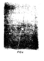
- Figure 4 is a photograph by a differential contrast interference microscopy of the exposed and developed assembly described in connection with Example 28.
- the photograph depicts a 300 micron square pattern feature separated by 75 micron spaces from adjacent 300 micron square features.
- four 1.5 micron spaced guiding lines 125 microns in length lead to a characteristic T pattern feature composed of 1 micron wide spaces separated by 2 micron size bars.
- the plurality of densely packed domains comprising the continuous film pattern feature are clearly evident in the polymerized film regions.
Abstract
Description
- This invention relates to photographic and photolithographic articles and for methods of producing such articles. The invention is particularly concerned with articles comprising a substrate and a layer carried thereby of a photopolymerizable composition comprising a photopolymerizable di or tri-acetylenic monomer. The photopolymerizable nature of diacetylenes in multilayers is known, see for example, Journal of Polymer Science, Polymer Chemistry Edition Vol 17, 1631-1644 (1979). This article discloses a series of amphiphilic diacetylene monocarbonic acids were synthesized and their ability to form monolayers at the air-water interphase was investigated. Acids with total number of carbon atoms greater than 20 and a melting point greater than 45°C form surface states suitable to be used for build-up of multilayers by the Langmuir-Blodgett technique. Using the LB technique, multilayers of defined thickness were built up on quartz substrates. The multilayers were polymerised by exposure to an ultra violet light source according to the mechanism of solid state polymerization of diacetylenes without destruction of the layer structure and with retention of the packing in the individual layers. Thus well-defined polymer multilayers were obtained. The monomer and polymer multilayers were characterised by ultra violet spectra, x-ray small-angle diffraction and interference microscopic and electron microscopic techniques.
- These diacetylenic compositions offer vastly improved properties for photography and photo- lithography as compared with the materials known hitherto.
- Photo-lithography finds its roots in 1852 when British Patent No. 565 was issued to Talbot for a bichromate sensitized gelatin coating which was useful for differential etching of copper by ferric chloride. Since this time, numerous compositions and processes have been developed which serve to transfer a pattern of light or other radiant energy onto a substrate through the intermediation of a coating sensitive to such radiant energy. The art of photolithography has developed broadly in recent decades to include various modes of printing, etching, and image reproduction from macro to micro scales, and has fostered the development of entire new industries. See generally, Photo-Resist Materials and Processes by William DeForest, McGraw-Hill 1975.
- One industry which has placed heavy reliance upon the use of photolithography is that of microstructure fabrication. This industry which produces structures imposed upon surfaces of thin films having extremely small dimensions is the basis for the production of information processing, electronics, switching, and other devices which rely upon "integrated" electronics, the fabrication and interconnection of large numbers of very small device structures on a single piece of silicon or other substrate.
- Exemplary uses of photolithography employing what is commonly denominated in the art as photo- resists, are described in Science, Volume 196, No. 4293, pp 945-949, 27 May 1977, by R. W. Keyes. As taught in the Keyes article, a substrate, usually . silicon, is caused to be coated with a layer of electrically non-conductive material, frequently silicon dioxide, usually by "growth" from the substrate itself through a suitable oxidizing process. The substrate is then further coated with one or more layers of photo-resist. At this time, selected portions of the photo-resist are exposed to a suitable form of radiant energy, which irradiation causes an alteration of the structure or physical characteristics of the portions of the resist thus exposed. Thus, electromagnetic energy such as light, especially ultraviolet light; X-radiation, laser radiation, etc. and particle radiation such as electron beam, particle beam, and plasma radiation may be utilized to alter the structure or physical characteristics of the portion of the photo-resist irradiated.
- Following the irradiation of the selected portions of the photo-resist and concomitant alteration of the structure or physical characteristics thereof, a distinction may be drawn between the selected portions of the resist and those not selected based upon the altered structure or physical characteristics.
- Thus, the selected portions may be viewed as being either more or less suited to removal from the underlying substrate than are the unselected portions through any appropriate means. The selected portions may be either more or less soluble in a liquid medium, may have a higher or lower vapour pressure, may exhibit greater or lesser resistance to chemical attack, or may evidence any other differing structure or characteristic which may facilitate differential removal from the substrate as compared to the unselected portions. Based upon one or more of these distinctions, the selected (irradiated) portions of the photo-resist are either removed from the substrate while the unselected (unexposed) portions remain, or the selected portions are retained while the unselected portions are removed. By analogy with traditional photographic processes, the former process is carried out with photo-resists denominated as "positive" resists while the latter employ "negative" photo-resists.
- The selection of certain portions of a photo-resist for irradiation may be accomplished in various ways, all of which are well known to those skilled in the art. Masking is a common procedure which is performed by placing over the surface of a photo-resist-coated substrate (or composite . substrate) a mask, usually formed photographically, and by causing the passage of radiation through the mask onto the resist layer. The mask is designed so as to have transmissive and non-transmissive areas corresponding to the portions of the resist layer which have been chosen for imadiation and for non- irradiation respectively. As is well known tothose skilled in the art, the radiant energy used in conjunction with the masking technique may benefit from being coolimated, focused, monochromatized, or rendered coherent. Such persons will also recognize that all portions of the electromagnetic spectrum may be employed with the masking technique as may various forms of particle irradiation such as electron beams, ion beams, and plasma irradiation.
- It is also well known to irradiate selected portions of a resist layer without the use of masking. Thus direct projection of a radiant energy beam, especially a laser, electron, or particle beam may be andertaken to irradiate the selected portions of the layer. Such projection is usually controlled by automated means and often by a computer. It is to be understood that the means and mechanisms for- irradiating selected portions of the photoresist layer are well known in the art. See, for example, proceedings of the IEEE, volume 62, No. 10, pp 1361-1387, October, 1974, Henry I. Smith, Fabrication Techniques for Surface-Acoustic-Wave and Thin-Film Optical Devices; X-Ray Optics: Applications to Solids (Ed. H.J. Queisser); E. Spiller and R. Feder, X-ray Lithography, pp 35-32 Springer (1977); and Ann. Rev. Mat. Sci., vol. 6, pp 267-301, L. F. Thompson and R. E. Kerwin, Polymer Resist Systems for Photo-and Electron Lithography.
- It may be seen that following the irradiation of the selected portions of the photo-resist and the selected removal either of the selected portions or of those portions not selected, a pattern will remain on the substrate formed of irradiated or nonirradiated photo-resist depending upon whether a negative or positive resist formulation was employed.
- This photo-resist pattern will alternate with exposed substrate, usually silicon oxide. The exposed silicon oxide (or other) substrate layer segments or portions are then subject to treatment. In nearly all cases, the oxide layer is removed or etched away in manners well known to those skilled in the art.
- The etching away of the silicon oxide layer is designed to expose the underlying silicon substrate to treatment and processing. The etching of the silicon oxide layer is intended to be accomplished only in the areas not covered with portions of photo- resist. The photo-resist must therefore be relatively insensitive to the etching means employed to remove the exposed oxide portions.
- After the etching off of the oxide layer the remaining photo-resist is removed to yield a pattern of exposed silicon and silicon oxide or other substrate formulation. The exposed silicon is then treated to alter its electrical characteristics, frequently through processes denominated as "doping". "Doping", which is well known to those skilled in the art, causes elements such as phosphorous or boron to be diffused into the exposed silicon or other substrate material. The treatment of the article after the removal of the photo-resist is not directly related to this embodiment of the invention and is well known to those skilled in the art. The treated article may subsequently be re-coated with photo- resistive materials, exposed selectively, and caused to undergo differential removal of resist, etching, and treatment one or more additional times to result in complex surface structures on the substrate. A selectively exposed and removed resist layer may also be used for the deposition of metal or other conductive materials onto the surface of the substrate to serve as electrical contacts with the variously treated surface areas as is well known to those skilled in the art.
- It is to be understood that the foregoing background is not intended as a rigorous delineation of the metes and bounds of the microfabrication art and that numerous variations, both of materials and processes are known. It should be further understood that the term "photo-resist" has been adopted by these skilled in the art as a generic term descriptive of all forms of radiation - sensitive coatings useful in lithography. Thus, the term embraces coatings useful for microfabrication, etching, printing, and compositing as well as numerous others. Similarly, the term "photo-resist" has been adopted for those coatings which are sensitive to particulate radiation such as electron beams.
- It is apparent from the foregoing that the characteristics of the photo-resists useful in a particular photolithographic process is of central importance to the success of that process.
- It will be appreciated, therefore, that there is a need for a photo-resist which is capable of ultra-fine resolution, exhibits a high response to incident radiation, easily applied to substrates, coats such substrates uniformily and adheres to them firmly until removal is desired. Furthermore, it is desirable that the resist, when exposed to incident radiation, should undergo a substantial change in physical properties, thus to provide a clear distinction between the exposed and unexposed portions so as to facilitate the selective removal of one or the other from the substrate when desired.
- According to the present invention, there is provided a photographic or photolithographic article comprising a substrate, and a layer carried by said substrate of a photopolymerizable composition characterised in that said layer comprises at least one material having at least two acetylenic bonds, at least two of said bonds being in conjugation with one another, and having a plurality of discrete domains.
- The invention also includes a method of making the article of the invention, which method comprises coating a substrate with at least one substantially continuous layer of a photopolymerizable composition characterised in that said layer comprises at least one material having at least two acetylenic bonds at least two of said bonds being in conjugation with one another and having a plurality of discrete domains.
- In one embodiment of the present invention, the article may comprise a plurality of domains within which a majority of the molecules of the- monomeric material are oriented in a regular array. The orientation of the molecular array in one of said domains is preferably transverse to the orientation of the molecular arrays of the majority of domains contiguous thereto. It is preferred that the domains have an average dimension of not more than 10,000 angstrom units and more preferably, not more than 2,000 angstrom units. In one embodiment of the invention the domains may have an average dimension in the plane of the layer of less than 1,000 angstrom units.
- The discrete domains may include molecules of lower polymerisability than said material. The said material may further include molecules which have a steric structure or substituent groups which reduce the polymerisability thereof.
- The photopolymerisable layer may also include a substituent grouping or groupings which bond covalently with the substrate; these substituent groupings may be silyl or siloxyl linkages. In a further embodiment of the invention, a bonding layer may be interposed between the layer of photopolymerisable composition and the substrate therefor, said bonding layer being covalently bonded at least to the layer of photopolymerisable composition. The bonding layer may comprise a compound having the general formula

- A typical example of such a compound is 3 aminopropyl triethoxysilane. The layer may further include a nitrosodimer to retard thermally induced polymerisation without interferring with the domain structure or with the photopolymerisability of the material per se.
- The domain structure may be established within the photopolymerisable material by heating the material after forming the layer on the substrate to a temperature below the melting point of said material to establish the discrete domain. In one embodiment of the invention the layer formation may be effected using the Langmuir-Blodgett film forming technique characterised in the pH temperature and/or the specific gravity of the water sub-phase used in the technique is adjusted to cause or allow formation of said domains in the resulting layer.
- As indicated above, in order to advance the art of technology known as "the silicon chip" technology as discussed above, it is clearly apparent that photoresistive layers and compositions and articles are necessary which have greatly "improved efficiency, permeability, structural regularity, resolution, contrast and adhesion to substrates.
- It will be appreciated that an improvement in resolution means that smaller structures can be prepared on a given size of micro chips surface. The particular problem hitherto has been that with an amorphous polymer resist, they undergo a physical "relaxation" phenomena which leads to microstructural line indistinction and to a lowering of resolution. When an image is projected on to such a photoresistive layer, the image of the microstructural line pattern will be sharp and extremely distinct. The exposed areas of the photopolymerisable composition will polymerise and polymerisation will occur across the boundaries of the microstructural line image projected onto the surface, thus resulting in a blurring of the image on removal of the coating during processing or "development" of the photoresistive image.
- The present invention seeks to overcome this particular problem by seeking to form discrete "domains" of groups of photopolymerisable molecules within the layer into specific "domains". As hereinafter described in order for the photopolymerisation reaction to take place effectively, the molecules need to be oriented at least to some extent for that photopolymerisation reaction to proceed.
- The Applicants have realised that by confining and controlling the areas of onentation, the resolution of the resulting photoresist can be controlled. Thus, by reducing the size of the "domains" to the order of 1,000 angstroms units or less, the Applicants have found that they are able to improve very significantly the micro-structural resolution of photoresists images over and above that described hitherto. This permits the use of shorter wavelengths radiation which in itself permits improvements in the resolution of the microstructural lines in the photoresist image. For example, X radiation in use at the present time on prior art photoresistive compositbns permits resolution of structures of not much below 10,000 angstroms. In contradistinction, the present invention permits the resolution of microstructures line of the order of below 10,000 angstroms, usually below 2 to 3,000 angstroms; in extreme circumstances, the resolution of structures as small as 100 angstrom units may be obtained. This dramatic improvement in resolution leads, therefore, to an immediate increase in the number of microstructures which may be fabricated on a given surface area of substrate and this in term permits the reduction in size of articles such as microchips made thereby and leads to a substantial economic advantage in all forms of electronic control equipment relient upon such articles.
- Following is a description by way of example only and with reference to the accompanying drawings of methods of carrying the invention into effect.
- In the drawings:-
- FIG. 1 is a schematic representation of the polymerization of the compositions of the invention according to the processes of the invention, whereby a mechanism is postulated. The regularity of assemblages of monomer and of the resulting polymer is shown.
- FIG. 2 is a representational view of certain embodiments of the present invention, especially photographic film. Thus 1 represents a coating comprising the materials of the invention, while 2 refers to a substrate which may comprise either one or a plurality of layers. It is to be understood that
coating 1 may be a monolayer, multilayer, or other coating. Additionally,substrate 2 may comprise inhomogeneous material or aggregates. In one embodiment,substrate 2 comprises a flexible film while coating 1 is one or more layers, of diacetylenic materials; in another, 2 is doped silica, and - FIG. 3 is intended to suggest the domain micro structure of certain preferred embodiments of the invention. Thus, domains such as those indicated by 3, are present, which domains have substantially regular arrays of constituent molecules. The orientations of these arrays are to be implied from the hatching placed thereupon. Reference No. 4 is intended to suggest the average dimension of a domain according to preferred forms of the invention.
- Figure 4 is a photograph obtained by differential contrast interference microscopy of an exposed and developed article in accordance with the invention as described in the following Example 31.
- In general, the invention is useful in the formulation, application and use of photographic, photolithographic and photoresistive compositions. Thus, the invention provides for novel means of photography, macro and micro lithography, printing, etching and engraving and for the elaboration and fabrication of micro structures, especially those useful in the electronics and integrated electronics fields. In addition, the use of certain genre of chemical compositions in the processed of the invention is taught together with the elaboration and fabrication of articles utilizing the novel compositions and processes taught herein.
- ; The photo-resistive articles of the invention are characterised as demonstrating superior performance in the elaboration and fabrication of electronic microstructures, as requiring lesser amounts of radiant energy in use, and as enabling a significantly more detailed resistive pattern structure to be composed upon the surface of a substrate. Thus, the processes of the invention utilize a genus of photo-resistive material which is energy efficient. This energy efficiency may be demonstrated by comparison of an X-ray photo-resist recording to the present invention with typical members currently in use in the art. It has been reported
- that from 1 to about 60 joules per cubic centimeter absorbed dose is required for currently used negative X-ray resists. In contrast, the composition of the invention require only about 0.001-0.01 joules per cubic centimeter for polymerization. This high efficiency is manifested by short exposure times and concomitant savings in radiant energy output, in time, and in production costs.
- The materials used in the invention are negative in mechanism, that is, upon exposure to radiant energy, they polymerize to form areas of polymer which are differentially retained upon exposure to a solvent as compared to the unexposed areas of photo-resist. The materials are further characterised as having a physical and electronic structure which is uniquely suited to polymerization thus exhibiting an excellent overall efficiency or quantum yield of polymerization upon exposure to radiant energy.
- A further aspect of the composition used in the practice of the invention also stems from the unique physical and electronic structure of the composition. The regularity exhibited by the compositions is such that extremely fine exposure patterns may be resolved in the photo-resistive materials formed thereby. For example, X-ray photoresistive compositions currently in use permit resolution of structures on the order of 10,000 A o and to 2000-3000 A in extreme cases. The compositions of this invention may be employed to permit o resolution of structure as small as 100 A. This improvement in resolution leads to an immediate increase in the number of microstructures which may be fabricated on a given surface area of substrate. This increase permits the reduction in size of articles made thereby and leads to substantial economic advantage.
- As stated above, amorphous polymer resists undergo physical "relaxation" phenomena in certain systems which lead to microstructural line indistinction and blurring. Additionally, it is known that most systems known to the prior art experience some dissolution of polymer intended to remain during the dissolution and removel step thus leading to edge undercutting. The articles of the present invention are ideally suited to overcome these problems however. Upon exposure to incident radiation the compositions polymerize into regular polymers with great facility and with high efficiency.
- The resulting polymers possess physical properties which are vastly different from the unpolymerized compositions. Especially significant is the large difference in solubility between the species; indeed the polymerized compositions are virtually insoluble in commonly employed solvents as compared with the unreacted compositions. As a result, therefore, the unexposed, and consequently, unpolymerized, areas are removed almost entirely by exposure to solvent while the exposed regions remain almost totally intact and in place. At the same time, the extreme regularity of the polymerization process together with the domain structure of the photopolymerisable layer and the geometric similarity of the polymers thus formed to their constituent monomers minimizes the"relaxation" experienced by the system upon polymerization. Thus line definition is sharp and blurring avoided.
- The compositions of the invention need not employ a sensitizer although one may be employed if desired. Furthermore, the processes of the invention may employ coating techniques which lead to extreme uniformity of substrate coverage and result in similar uniformity of lithographic resolution and clarity.
- One embodiment of the present invention includes materials which liberate radical trapping agents upon the application of heat.
- -Such compounds, such as dimers of nitroso compounds which are known in the ethylenic system (see U.S. Patent 4,168,982) serve to reduce thermal polymerization and avoid "undercutting". It has been discovered that diacetylenic systems are particularly benefitted by their inclusion.
- The compositions employed in the processes of the invention demonstrate superior adhesion to substrates and exhibit a high degree of dissimilarity in physical properties upon polymerization thus leading to ease of processing and superior results. Indeed a preferred form of the invention employs siloxyl moieties to form covalent bonds between the photo- resistive layer and the substrate to result in extremely good adhesion between the substrate and the resist. Other forms of covalent bonding may also be employed.
- The utilization of the materials and processes of this invention in photographic systems such as, for example, in photographic films is similar in some respects to use as a photoresist. Thus, thin film or collections of films employing the materials of the invention may be employed as either a direct print positive photographic film, or as a negative film. The variety and intensity of colours which are known to be possessed by these materials upon polymerization lend them to colour photography, while their extreme resolution and sensitivity result in photographic materials of unparalleled resolving power and efficiency.
- Briefly stated, the compositions useful in the practice of the processes of the invention comprise photoresistive materials comprising one or more members of the class of chemical compounds known as diacetylenes. Diacetylenes may be seen to possess at least two carbon-carbon triple bonds (acetylenic bonds) at least two of which triple bonds are in conjugation one with another, i.e. exist in a 1-3 relationship as is illustrated:
-

- As is known to those skilled in the art, an acetylenic bond possesses a generally linear geometry. It follows that diacetylenes possess a generally linear arrangement of six atoms, the four carbon atoms participating in the diacetylenic "backbone" and each of the two atoms bonded to either.end of that backbone. In addition, it is apparent that the diacetylenic structure, being rich with electron density; possesses a novel electronic structure. It is this electronic and geometric structure possessed by the genus of diacetylenes which is believed to contribute in major degree to the unique suitability of such compounds for inclusion in photoresistive and other compositions as taught by this invention.
- Diacetylenes which are suitable for use in the practice of this invention conform to the general formula:

- In short, it is contemplated that any diacetylene may be suitable for use in the practice of one or more of the embodiments of the invention with the exception of those diacetylenes wherein R1 or R2 or both are hydrogen. The latter compositions are not suitable due to the fact that they are, in general, explosive.
- it is to be understood that the species referred to in this description of the invention may be either straight chain, cyclic, aromatic, or branched. It should also be understood that reference to the composition of this invention as being diacetylenes does not foreclose the presence of additional acetylenic bonds therein. Thus, compositions having 3, 4, or more acetylenic bonds are foreseen as long as at least two or more of such bonds are in conjugation one with another. Furthermore, additional sites of unsaturation may be present such as carbon-carbon, carbon-oxygen, carbon-nitrogen, or other double bonds, aromatic or heteroaromatic species. Substitution with halogens, hydroxyls, amines, thiols, silyls, siloxyls, phosphates, sulfates, sulfonates, or other functionalities is also useful.
- For the practice of certain embodiments of the invention, diacetylenes may preferably possess the general formula:


- n is an integer from one to about 10 and preferably one to three; and A is a member of the group consisting of halogen, COOH, COOR6, CONH2, CONHR6, OH, SH, NH2, NHR6, N(R6)2, silyl, siloxyl, sulfate, sulfonate, phosphate and others where R6 is a hydrocarbon having from one to about 8 carbon atoms. Certain preferred forms of the composition include styryl moieties in the hydrocarbon portion of R3 or include other polymerizable unsaturations such as, for example, dienyl, vinyl or acrylic species.
- Certain embodiments of the invention may usefully be accomplished utilizing compositions of the formula:


- Additional embodiments of the invention may profitably employ diacetylenes of formula (I) where R1 or R2 or both have the formula:


- In some embodiments of the invention, especially those in which polymerization by UV or Z-ray radiation is desired, it has been found convenient to include a number of heteroatomic species in the compositions of the invention. Thus halogens, especially fluorine, sulfur, selenium, phosphorus and similar atoms are preferably included. This is done to improve the cross section of energy which may be absorbed by the composition, thus to improve its overall efficiency. Of especial note is the employment of polyfluoroalkyl substituents in the practice of the invention for this purpose; specific use of such moieties is contemplated hereby.
- It should be apparent from the foregoing that no limitation is intended or is to be implied with respect to the diacetylenes suitable for the practice of one or more embodiments of this invention. All compositions which include one or more chemical species having at least two acetylenic bonds, at least two of which are in conjugation one with another are suitable.
- Exemplary syntheses of diacetylenes are presented in "Synthesis of N-(nitropheynl)amine Substituted Diacetylene Monomers", Garito et al, Makromolecular Chemie (in press); "Synthesis of Chiral Diacetylene Polymers", Garito et al, Makromolecular Chemie (in press); "The Chemistry of Diacetylenes", Keter Pub. House, Jerusalem (1974); "Synthetis of Nitrophenoxymethyl Substituted Diacetylene Monomers", Kalyanaraman, Garito et al*, Makromolecular Chemie, vol. 180, June 1979; "Solid-State Synthesis and Properties of the Polydiacetylenes", Baughman et cl, Annals of NY Academy of Science, vol 313, (1978); "Polymerization of Diacetylene Carbomic Acid. Monolayers at the Gas-Water Interface", Day et al, J. Polymer Sciences, Polymer Letters ed. vol. 16, p. 205 (1978); and U.S. Patent 3,923,622 issued to Baughman et al.
- As a class, diacetylenes exhibit uniquely regular structure in thin films, multi-layer films, and polymers formed therefrom. In thin films formed on substrates, diacetylenes assume a regular orientation. Upon polymerization, this regular orientation is, to a large degree, maintained resulting in polymers having a regular orientation. This phenomenon which is illustrated in FIG. 1 is known.
- The chemical molecular structure of such polymers, while not entirely clear, is subject to interpretation. As shown in FIG. 1, polymers of diacetylenes are believed to possess triple and double bonds in a 1-3 relationship in the subunits of the polymer. It will be understood by those skilled in the art that the two "resonance structures" indicated for the polymer represents the fact that, with poly(diacetylenes) as with most organic molecules, structural description in terms of bond order, i.e. triple, double, etc. is less than precise. Thus, with the understanding that the polymers possess bond characteristics which are not fully representable as any one single structure, such polymers will be described as having an acetylenic bond in the subunit thereof. The polymers may be alternatively described as having a repeating subunit wherein four carbon atoms are aligned in a generally linear configuration. Thus, the polymers produced according to the practice of this invention may be alternatively described as 1) being substantially regular in orientation, at least within any polymer domain; 2)'having an acetylenic bond in the subunit structure thereof, and 3) possessing subunits which have four carbon atoms in a generally linear configuration.
- In general, it is possible to coat substrates with diacetylenes and to utilize such coatings for photo-resistive and other purposes. It is believed that the regular orientation of the diacetylenic "backbone" in the layers so formed places the acetylenic bonds in the proper orientation for polymerization to proceed with high efficiency.
- This factor combined with the amenability of diacetylenes to absorb radiant energy and to undergo photolytic generation of reactive intermediates such as radicals or carbenes causes such oriented arrays of diacetylenes to be highly reactive towards incident radiation and to effect polymerization quickly upon irradiation.
- Coating of substrates with diacetylenic compositions is preferably accomplished by the Langmuir-Bldgett technique. This technique, which is well known to those skilled in the art, causes a thin film of diacetylene to be deposited upon the surface of a fluid. The surface layer is then compressed to minimize the surface area occupied by the diacetylene so as-to effect a closest packing arrangement thereof. This closely packed and arrayed diacetylenic composition is then transferred to a substrate by dipping. The use of diacetylenes having hydrophobic and hydrophilic substituents on either end thereof facilitates the use of the technique. These multi-layers may be uniform in composition or may be dissimilar. They may number from two to several hundreds and may, thus, comprise thin or thick films.
- Alternative means of placing diacetylenes on substrates may be utilized as well. Thus, the "whirling" technique as described in the DeForest reference, roller coating as is currently practiced in the art, or even dipping may be employed so as to apply the diacetylenic species to the substrate.
- Coating by vapour deposition may also be employed. The thickness of the films employed in the practice of the current invention may vary depending upon the use contemplated therefore. From a few to about 40 Langmuir-Blodgett constructed layers or a comparable thickness of film formed by one of the alternative means is most suited to photo- resistive purposes while greater or lesser thicknesses lend themselves to other embodiments such as photography.
- The composition useful in the practice of the invention may include species in addition to the aforedescribed diacetylenes. Thus, additional polymerizable materials may be added as may catalysts, photo-initiators, pigments, and fillers. Additionally, organic or inorganic materials may be included to alter the electrical properties of the compositions, especially for use in thin film devices. The additional polymerizable materials which may be included may encompass any of the wide variety of polymerizable species known to those skilled in the art. Olefinics such as vinyl, styryl, acrylic, dienyl, etc. are preferred. Of these, dienyl and acrylic species are preferred. Dimers of nitroso compounds may also be included as indicated above.
- The composition may, optionally, contain a sensitizer or catalyst to improve the photochemical interaction between the compositions and incident radiation. Such sensitizers are well known in the art and include, for example, acetophenone, acyloin derivatives, benzophenone, dyes such as indigo derivatives and many other species. The sensitizers may be included in amounts up to about 5 % by weight of composition and preferably between about 1% and about 3%. In an alternative embodiment, one or more layers of diacetylenic composition may be "sandwiched" with layers of sensitizer-containing formulation to give good results.
- Other compositions may include in the diacetylenic species polymerizable sites in addition to the diacetylenic bonds themselves. Thus, diacetylenic compounds having acrylic, sturyl, vinyl or other polymerizable functionalities may be used to good reslt. In such a case, the polymerization of such additional polymerizable structures may be accomplished concomitantly with or subsequent to the polymerization of the "backbone" diacetylenes. In cases where multiple single layers of oriented diacetylenes are laid down upon a substrate, it may be seen that polymerization of the "backbone" "may occur almost exclusively within one layer. The presence of other polymerizable species creates the possibility of inter-layer polymerization or cross linking. The inclusion of styrene residues is especially preferred for this purpose.
- For the practice of photography and photo- lithography it is highly desirable to employ photosensitive materials which combine high resolution with high sensitivity to radiation. Such goal is attained by the present invention through the use of ordered arrays of diacetylenic films of high sensitivity which have been arranged in a plurality of domains.
- It is believed that the substantially regular array evidenced by the diacetylenic films according to the practice of this invention, especially those elaborated by the Langmuir-Blodgett technique, contribute to high photoreactivity of those films as reflected in the high quantum efficiency alluded to above. While such high efficiency is to be desired from the point of view of speed of reaction and overall savings of energy in use, it will be appreciated that such high efficiency appears to be contrary to the twin goal of high resolution. A photoresist having the high efficiency of the present invention would be expected to evidence uncontrolled polymerization or reaction upon exposure to radiation and to react not only in exposed areas, but also in neighbouring, unexposed areas as well.
- -The present invention overcomes this difficulty and provides photoresists having both a very high efficiency and a high resolving power.
- This goal may be obtained through a technique whereby substantially ordered or arrayed films on layers of diacetylenes are caused to be arranged of diacetylenes are caused to be arranged in a plurality of domains within the film or layer structure. It will be appreciated that a substantially regular array of molecules will be retained within the domains thus provided, but that the domains will be randomly oriented so that a domain's molecular array orientation will not normally be repeated in the array orientation of its neighbours. Thus, within any domain, a substantialy regular array of diacetylenic molecules will prevail, but that array will terminate at the domain boundary. It will be apparent from the foregoing that the sensitivity of the diacetylenic species arrayed within a domain will remain largely unchanged, but that a photolytic reaction initiated in one domain will not normally pass over into neighbouring domains. It will be similarly apparent that the above embodiment will yield photographic materials and films of high sensitivity, and resolution.
- The arrangement of diacetylenic films into a plurality of domains may be accomplished in a number of ways. Thus a substantially ordered film or layer of diacetylenic material may be heated either conventionally, through laser or microwave heating techniques, or in other ways to accomplish the establishment of the domains. With conventional heating, heating to just below the melting point of the layer is preferred. Alternatively, during the employment of Langmuir-Blodgett film-forming techniques, one may adjust the pH, the temperature, or the specific gravity of the water subphase utilized in the process to cause the assumption of domains in the resulting
- It is believed that the size of the domains produced in the practice of the invention will be reflected in the ultimate resolving power of the photoresist. In practice it has been possible to create domains of average dimension well below 1000Å but larger and smaller domain sizes are specifically envisioned as well. Thus, preferred embodiment include domains having average dimensions less than about 10,000Å, and even more preferably less than about 2000Å.
- An alternative procedure to the establishment of domains in the diacetylenic layers is to include molecules of lower polymerizability in the compositions. These molecules may be any of a wide range of materials including certain of the less reactive diacetylenes, long chain olefins or fatty acids. Alternatively, diacetylenic species may be chosen which possess steric or electronic structures which are not entirely favourable to polymerization either by upsetting the substantially ordered array present in the film or layer or by presenting molecules or lesser reactivity to the advancing polymer chain. Such inclusions may be seen to "temper" the reactivity of the films or layers and to provide an alternative means of control of the system.
- For certain applications, it is highly beneficial to provide a strong adherence of the coatings to the underlying substrate. It is possible to bond such coatings to substrates covalently utilizing certain techniques. Thus, hydroxyl or other functional groups commonly found on the surfaces of most substrates may be utilized to consummate silyl or siloxyl linkages with a suitably silicon substituted diacetylenic species. See E.P. Plueddemann, "Mechanism of Adhesion Through Silane Coupling Agents" in Composite Materials, Brautman, Krock eds, vol. 6, ch. 6, Academy Press (1974). Other means of covalent bonding of film to substrate or of film precursor species to substrate will readily occur to those skilled in the art. Thus, it is desirable to coat the substrate with a composition which may form covalent linkages with such substrate and which may also form covalent linkages with the diacetylenic species which comprise the photoresistive layer. While any composition which will form the covalent bonding may be employed, preferred species for accomplishing such covalent bonding may be represented by the formula:

- It has also been found that certain nitroso dimers such as 1-nitrosooctadecane dimer, 1-nitrosodo- decane dimer and 1-nitrosocyclohexane dimer may be included in the photoresistive compositions of the invention to retard thermally-induced polymerization without interfering with the photochemical polymerizations central to use of the materials as photoresists. In this regard, it is believed that the dimer dissociates thermally to species which inhibit polymerization. Thus thermal polymerization is hindered while photochemical polymerization is unaffected. Any other species which reacts thermally to provide radical - trapping species is also useful in this regard.
- 'It should be apparent that any form of irradiation may be utilized to effectuate the polymerization of the composition of the invention. Of the forms commonly used, particle beam, electron beam, X-ray, laser and ultraviolet irradiation are most preferred. As should similarly be apparent, irradiation with masking, with a controlled beam or without effective spatial control, that is, whole surface irradiation may be utilized in the practice of one or more embodiments of the invention. In general it is expected that substantial polymerization will occur within irradiated areas of the process of the invention. Substantial polymerization occurs when at least 50% of the monomer species become incorporated in polymer moieties. Preferably 75% and even more preferably 85% or greater incorporation is desired. In the construction of devices which include diacetylenic polymer films as constituents, it may be desirable to polymerize areas uniformly. As has been shown, a selective exposure is desirable for photo lithography and micro-fabrication. Thus either mode of irradiation may be seen to be useful.
- For employment as photographic media, it follows that for many uses, response to visible (or infrared) light is frequently desired. Thus the films or other materials may if necessary employ any of the well-known sensitizers to alter the spectral response of the materials and products. Of course, the diacetylenic species which possess inherent sensitivity in the visible (infrared) region are suitable for such use without the use of a sensitizer.
- To a solution of propargyl alcohol (10 g) in DMSO (10 ml) K2CO3(1.5g) was added and the mixture kept stirring. 4-Nitrofluorobenzene (28 g) was added gradually and the mixture stirred at room temperature for three days. It was poured into excess water slightly acidified with HCl. TLC showed two spots, one of which was identical with 4-nitrofluorobenzene. Fractional crystallization from cyclohexane afforded a pale yellow solid (15.8g, 50%), m.p. 103-110°C; I.R. (KBr): 3174(=CH), 1582, 1315, 847 (ar-NO2)cm-1.
- A solution of the material from Example 1 (1 g) in DMSO (15 ml) was added at 55-60°C, with stirring, to a mixture of cuprous chloride (1g.) and ammonium chloride (3 g) in water (10 ml), with oxygen passing through the solution. After four hours, the mixture was poured into dilute aqueous ammonium hydroxide solution (500 ml). The yellow ppt. was filtered off, washed with cold water, dried and recrystallized from dioxane-ethanol (1.3 g, 70%), m.p. 213°C dec.; I.R. (KBr): 1532, 1336, 847 (Ar-NO2) cm-1
- To a solution of 2,4-hexadiyne-l,6-diol (5 g) in DMSO (15 ml), triethylamine (2 ml) was added. To the stirring solution at room temperature, 2,4- dinitro-1,5-diflouoro-benzene (20 g) was added gradually. After stirring overnight at room temperature, the mixture was poured into water, the product filtered off, washed with water, dried and recrystallized from dioxane-water (16 g., 75%). The compound decomposes above 190°C without melting. I.R. (KBr): 1587, 1333, 846 (Ar-NO2), 1176 (Ar-F)cm-1.
- Reaction of 2,4-hexadiyne-1,6-diol (1 g) with 4-fluoro-3-nitro-benzotrifluoride (4 g.) following the procedure of Example 3 yielded the desired product.
- Recrystallization from ethanol gave pale yellow needles. (1.1 g., 25%) m.p. 137°C. I.R. (KBr): 1620(NO2), 1120 682 (CF3)cm-1.
- To a solution of KOBr in water (from 22 g. KOH, 5 ml. Br2 and 100 ml water) at 0°C, 4-nitrophenyl propargyl ether (3.5 g) in dioxane (80 ml) was added dropwise with stirring. After stirring an additional 15 minutes, the solution was poured into excess ice water and the precipitate was filtered off and recrystallized from dioxane as a white powder (4.5 g., 90%), m.p. 156-157°C. I.R. (KBr): 1587, 1324, 847 (Ar-NO2)cm-1.
- To a suspension of cuprous chloride (20mg), ethylamine (70%, 1.4 ml) and hydroxylamine hydrochloride (0.12 g) in water (5 ml), a solution of propargyl alcohol (1 g) in DMSO (2 ml) was added with stirring. To the yellow mixture, the bromo ether of Example 5 (0.6 g.) in DMSO (20 ml) was added dropwise at 20°C over 40 mins. After stirring for an additional one hour, the solution was poured into excess water, the yellow precipitate filtered off and recrystallized from methanol as short needles (0.4 g., 74%), m.p. 172-173°C. I.R. (K3r): 3448-(-OH), 1582, 1333, 846(Ar-NO2)cm-1.
- The material of Example 6 (0.23 g.) was dissolved in DMSO (3 ml) and triethylamine (0.5 ml) was added to the stirring mixture at room temperature, 2,4-dinitrofluorobenzene (0.2 g.) was added dropwise. After stirring for four hours, the reaction mixture was poured into water, the precipitate filtered off and recrystallized from dioxane to afford pink crystals (0.35 g., 88%), m.p. 125°C. I.R. (KNr): 1589, 1333, 846(Ar-NO2)cm-1.
- To a suspension of potassium carbonate (20.0 g) in DMSO (7 ml) was added triethylamine (3 ml) and 2-propyn-1-anine (7.10 g, 1.29 x 10⁻¹ mole). 2-Fluoro-5-nitrotoluene (20.00 g, 1.29 x 10⁻¹ mole) was added with stirring and the reaction mixture was heated at 50°C for three days. The mixture was cooled, poured into excess water, and extracted with methylene chloride. The methylene chloride solution was dried over sodium sulfate, filtered and evaporated. The residue was chromotographed on a silica column, eluting with benzene, and recrystallized from benzene to afford yellow crystals; -m.p. 121-123°C. Yield: 15.02 g (61%). I.R. (KBr): 3344 (NH), 3226 (CH), 1580 and 1262 cm-1 (Ar-NO2).
- To a suspension of Cu(OAc)2.H2O (1.5 g) in pyridine-methanol (1:1, 15 ml) was added N-(2-propynyl) -2-methyl-4-nitroaniline (1.00 g, 5.26 x 10⁻³ mole). The reaction mixture was stirred at 50°C for two hours. The mixture was poured into excess water and filtered. The crude solid was recrystallized from nitromethane to afford yellow crystals. Yield: 0.70 g (71%). The material did not melt below 200°C but turned red at 150°C. I.R. (KBr): 3390 (NH), 1585 and 1280 cm-1 (Ar-NO2).
- To a suspension of potassium carbonate (20.0 g) in DMSO (7 ml) was added triethylamine (3 ml) and 2-propyn-1-amine (7.92 g, 1.44 × 10⁻¹ mole). The reaction mixture was cooled in an ice bath while 1-fluoro-4-nitro-2-trifluoro-methylbenzene (30.13 g, 1.44 x 10⁻¹ mole) was added gradually with stirring. The mixture was gradually allowed to warm to room temperature and stirred for 24 hours. The reaction mixture was poured into excess water and extracted with ethyl acetate. The ethyl acetate solution was dried over sodium sulfate, filtered and evaporated. The residue was chromotographed on a silica column, eluting with benzene, and recrystallized from benzene to afford yellow crystals; m.p. 71-72°C. Yield: 24.24 g (69%). I.R. )KBr): 3450 (NH), 3290 ( CH), 1588 (Ar-NO2) and 1300 cm-1 (CF3).
- To a suspension of Cu(OAc)2.H2O (4.5 g) in pyridine-methanol (1:1, 30 ml) was added N-(2-propynyl) -4-nitro-2-trifluoromethylaniline (3.01 g, 1.23 x 10⁻¹ mole). The reaction mixture was stirred at 50°C for two hours. The mixture was poured into excess water and filtered. The crude solid was recrystallized from nitromethane to afford pale pink crystals. Yield: 2.54 g (84%). The material does not melt below 200° C but turns dark red at 135° C. I.R. (KBr): 3405 (NH), .1580 (Ar-NO2) and 1290 cm-1 (CF3).
- To a suspension of potassium carbonate (6.0 g) in acetone (25 ml) was added triethylamine (1.5 ml) and 2-propyn-l-amine (2.35 g, 4.25 x 10⁻² mole). 1,5-Difluoro-2,4-dinitrobenzene (10.00 g, 4.90 x 10⁻² mole) was added and the reaction mixture was stirred at room temperature for 24 hours. The mixture was poured into excess water and filtered. The resulting dark solid was chromatographed on a silica column, eluting with benzene, and recrystallized from benzene to afford yellow crystals; m.p. 113-115°C. Yield: 8.33 g (82%). I.R. (KBr): 3340 (NH), 3280 ( CH), 1615, 1260 (Ar-NO2) and 1210 cm-1 (Ar-F).
- To a suspension of Cu(OAc)2.H2O (1.5 g) in pyridine-methanol (1:1, 10 ml) was added N-(2-propynyl) -2,4-dinitro-5-fluoroaniline (1.00 g, 4.18 × 10⁻³ mole). The reaction mixture was stirred at room temperature for 17 hours. The mixture was poured into excess water and filtered. The crude solid was chromatographed on a silica column, eluting with chloroform ethyl acetate. Soxhlet recrystallization of the resulting solid from ethyl acetate afforded yellow crystals, m.p. 225°C dec. Yield: 0.21 g (12%). I.R. (KBr): 3360 (NH), 1680 and 1315 cm-1 (Ar-NO2).
- To a solution of 510 mg (1.36 mmol) of 10, 12- pentacosadiynoic acid in 10 ml tetrahydrofuran was added 138 mg (1.36 mmol) of triethylamine. The resulting cloudy solution was cooled to 0°C and 129 mg (1.36 mmol) of methyl chloroformate was added dropwise over 1 min. A white solid formed immediately upon addition. The mixture was stirred 1 hour at 0°C, then 165 mg (1.36 mmol) of d(+)-α-methylbenzylamine was added and the mixture was heated at reflux for one hour. Gas evolution was evident within five minutes of addition, and ceased after 15 minutes.
- The mixture was cooled to room temperature and filtered. The filtrate was washed with 10 ml portions of 1M HCl, water, and saturated aqueous potassium bicarbonate solution, and dried (MgS04). Evaporation yielded 540 mg (83% crude yield) of a white solid. Recrystallization from ether - petroleum ether gave white crystals, m.p. 65.5-66.5°C. I.R. film: 1470, 1545, 1640, 2860, 2925, and 3310 cm-1. [α]D 31(CHCl3)= 44°.
- To a solution of 725 mg (2.00 mmol) of 10,12- docosadiyndioic acid in 50 ml THF was added 405 mg (4.00 mmol) of triethylamine. The solution was cooled to 0°C and 378 mg (4.00 mmol) of methylchloro- formate was added dropwise over one minute. The resulting white mixture was stirred one hour at 0°C,
- the 485 mg (4.00 mmol) of d(+,-α-methylbenzylamine was added. The reaction mixture was heated at reflux for one hour (gas evolution began immediately upon amine addition and ceased after 20 minutes). The mixture was cooled to room temperature and filtered. The filtrate was washed with 25 ml portions of 1M HCl, water, and saturated aqueous sodium bicarbonate solution and dried (MgSO4). Evaporation yielded 842 mg (74% crude yield) of a white solid, which polymerized rapidly upon exposure to UV light. Recrystallization from ether-petroleum ether gave 456 mg of white crystals, m.p. 87.5-89°C. I.R. (film): 1530, 1635, 2850, 2920, and 3300 cm-1.
- To a solution of 2,4-hexadiyn-1,6-diol (1.1 g) in acetone (15 ml), K2CO3 (0.5 g) was added. To the stirred solution at room temperature, 2,4-dinitrofluorobenzene (3.8 g) was added gradually and the dark red solution stirred overnight at room temperature. It was poured into excess water, the pale yellow solid filtered off, washed with water and dried. Recrystallization from dioxane ethanol gave short, light pink needles, m.p. 210°C (4.2 g, 95%). I.R. (KBr): 1592, 1333, 834 (Ar-NO2)cm-1.
- To a suspension of potassium carbonate (1.0 g) in acetone (10 ml) was added 2-propyn-1-amine (0.26 g, 4.73 x 10⁻³ mole). 2,4-Dinitrofluorobenzene (1.32 g, 7.10 x 10⁻³ mole) was gradually added with stirring and the reaction mixture was refluxed two hours. After cooling it was poured into excess water and filtered. Recrystallization of the crude solid from ethanol afforded yellow needles; m.p. 151-152°C. Yield: 0.99 g (95%). I.R. (KBr): 3367 (NH), 3268 (CH), 1618, 1590, 1333 and 1311 cm-1 (Ar-NO2).
- To a suspension of Cu(OAc)2.H2O (1.5 g) in pyridinemethanol (1:1, 10 ml) was added N-(2-propynyl) -2,4-dinitroaniline (1.00 g, 4.52 x 10⁻³ mole). The reaction mixture was stirred at 50°C for 30 minutes.
- The mixture was poured into excess water, and filtered.
- The crude solid was recrystallized from nitromethane to afford pale green crystals. Yield: 0.86 g (86%). The compound failed to melt below 200°C but changed from green to bronze colour at 120°C. It could be be recrystallized from dioxane to give a different crystal form, appearing as orange crystals which turn deep orange at 140°C. I.R. (KNr): 3380 (NH), 1617, 1592, 1333 and 1312 cm-1 (Ar-NO2).
- Diacetylene alkyl-acid monomers for use in mono- and multilayer preparations were synthesized by the Chodkiewicz coupling procedure using bromoacety- lenes prepared following Strauss. See Chodkiewicz, W. Ann. Chem. (Paris) 2, 853 (1957) and Strauss, et al, Ber. 63B, 1868 (1930). For example, 1-bromo- undecyn-10-oic acid was coupled to tetradecyne to form pentacosa-10, 12-diynoic acid. Fifty m. moles of tetradecyne dissolved in 5 ml ethanol was added with stirring to a 50 ml ethanol solution of 100 m.moles ethylamine forming a yellow solution. The stirred solution was cooled to 15°C and 50 m. moles of 1-bromo-undecyn-10-oic acid dissolved in 60 ml ethanol was added dropwise over 30 minutes while the temperature was maintained at 15-20°C. After the addition was complete, the reaction mixture was stirred for 3 hours at 15-20°C. The mixture was then acidified to
pH 1 and extracted twice with 100 ml ethyl acetate. The organic layer was separated, dried over magnesium sulfate, filtered through fluoro- sil and evaporated to give a colourless, viscous oil. The oil was taken up in methanol-petroleum ether and the solution was filtered. Upon cooling of the filtrate, pentacosa-10,12-diyoic acid crystallized as colourless platelets (m.p. 59-60°C). The platelets become an intense blue upon standing in laboratory light for a short time. - The apparatus used for multilayer preparation consists of a Langmuir trough made of Teflon with dimensions of 12.2 x 30 cm (area and 2 cm deep).
- The surface pressure is applied by a movable Teflon barrier connected to a motor driven screw gear. A Wilhelmy balance is used continuously to measure the surface pressure. The solid substrate is connected to a vibration-free solid rod and moved in and out of the trough using a reversibly geared motor at speeds of 1-3 cm/hr.
- A 4 x 10⁻³M solution of pentacosa-10,12- diyoic acid in n-hexane was spread on a 1 x 10⁻³M solution of cadmium chloride in water. The pH of. the CdCl2 solution was previously adjusted to 6.1 using sodium bicarbonate. Successive layers were deposited on the solid substrates at a constant surface pressure of 15 dyne per cm with a dipping speed of 0.5 mm/sec. Surface pressure area curves -show that near 23° C and a surface pressure of about 15 dyne/cm, a monomer molecule occupies 20 Å2. Y type deposition of the layers was observed.
- The amide produced in Example 14 was elaborated into a fourteen, Y-layer, multilayer assembly by the Langmuir-Blodgett technique on a ferric stearate- coated quartz plate and warmed in an oven at 60°C for two hours followed by slow cooling. The assembly was exposed to either UV or X-ray radiation through a mask giving excellent pattern delineation.
- In separate experiments, 12-30 layers of pentacosa-10,12-diynoic acid were deposited on solid substrate plates such as glass, silicon, and evaporated gold films on glass. Spatially defined regions of the multilayers were polymerized by X-ray exposure through a mask to produce negative resist device patterns on the substrate plates. For example, a 30 multilayer assembly of pentacosa-10,12-diynoic acid on a silicon single crystal substrate plate was positioned behind a metal mask to allow exposure of the multilayer assembly to X-rays through a 5 u wide by 1 cm long mask line. The total X-ray energy absorbed for polymerization and resultant pattern delineation was approximately 10 millijoules/cm3. After exposure, the remining monomer in the unexposed masked regions was dissolved away by rinsing in an organic solvent such as acetone leaving a well-defined line pattern composed of the pentacose-10,12-diynoic polymer on the silicon substrate. After substrate etching (processing) the polymer was removed by washing in a dilute aqueous HF solution.
- Silicon plates with an oxide layer .65u thick were immersed in concentrated nitric acid for 2 hours. After rinsing with water, the water contact angle (αw) was determined to be 44°. After thorough drying, the plates were treated with vapours of 3-aminopropyltriethoxysilane. The substrate was placed above a boiling solution of 2 ml of the silane in 100 ml dry p-xylene under nitrogen for 16 hours. The substrate was bathed in the vapour, the vapour condensing 5 cm above the substrate. The substrate was rinsed in absolute ethanol and water; αw was determined to be 45°. The silanated substrate was immersed in a solution of 22 mg (0.06 m.mol) of 10,12-pentacosadiynoic acid in 10 ml.. anhydrous pyridine. A solution of 14 mg (0.07 m.mol) of N,N-dicyclohexylcarbodiimide in 1 ml pyridine was added. The wafers were treated for 22 hours at room temperature under nitrogen. The substrate was rinsed with pyridine, ethanol, boiling pyridine, and boiling ethanol and dried. The αw was determined to be 78°.
- A multilayer assembly of 15 layers of the composition of Example 19 elaborated upon a quartz plate by the Langmuir-Blodgett technique was placed in an oven at 55°C for 6 hours and then cooled to room temperature. Pluralities of domains were thus established in the assembly which was found to yield excellent definition and response upon selective exposure to UV or X-ray radiation.
- Ordinary transparent, flexible film was coated with 15 Langmuir-Blodgett layers of the amide of Example 14. The coated film was heated at 55-60°C for 2 hours followed by cooling. The film was then exposed to a test pattern through a lens to afford excellent definition and resolution having a brilliant purple-bronze colouration.
- Large area multilayer films of disubstituted diacetylenes can be prepared conveniently using commercially available Langmuir film balances where the solid"substrates are relatively large, such as a single crystal semiconductor wafer several inches in diameter. One such commercial balance is a MGW Lauda Filmwaage Preparative Film Balance, Model P, which provides both continuous film isotherm measurements and compression to constant pressure of a monolayer spread at the air-water interface. An electrical feedback loop circuit between a floating Langmuir pressure balance and the movable barrier of the device maintains constant surface pressure as required for successive regular depositions of monolayer film onto solid substrates. Constant temperature of the water subphase is maintained (+ 0.2°C) by a constant temperature circulating bath and is measured at the air-water interface by a thermocouple surface probe.
- In all film depositions, the spread monolayer film was formed by delivering organic solutions containing the desired disubstituted diacetylene monomer in a dropwise manner at the airwater interface using a digital micropipette. Typical monomer solution concentrations were about 1.0 mg/ml in triply distilled solvent such as chloroform. Light sensitive films were deposited under yellow light conditions. In this manner, highly reproducible monolayer film areas and surface pressure-area isotherms were generally achieved.
- The solid substrate was held by a solid rod movable through the employment of a rubber isolated screwdrive synchronous AC motor to minimize mechanical vibration. Deposition speeds were generally on the order of about 3 mm per minute. No noticable vibrations were introduced at the air- water interface by the moving substrate as evidenced by the uniformity of the resulting deposited films.
- The foregoing apparatus was employed for the deposition of pentacosa-10,12-diynoic acid of Example 19 dissolved in triply distilled chloroform. The diacetylene solution was spread -in a dropwise manner, as described above, on a 1 X 10⁻³ molar solution of cadmium chloride in water (pH about 6.6) at a temperature of 17.5 +0.2°C. After the chloroform evaporated, the spread monolayer film was slowly compressed to a constant pressure of 25 dynes/cm. and deposited onto a 2 inch hydrophobic silicon wafer to form a multilayer assembly comprising 10 Y-type monolayers.
- Prior to deposition of the foregoing monolayers, it is preferred to render the silicon wafer hydrophobic. This can be attained through either of two well-known methods. A Langmuir-Blodgett deposition of several monolayers of a simple long chain alkyl-acid salt onto the hydrophilic oxidized silicon wafers could be performed. In the alternative, a reactive silane such as hexamethyldisilazane in either liquid or gaseous form could be reacted with the surface to render it hydrophobic through formation of a hydrophobic organosilane film. The latter technique is generally more convenient for most applications.
- A multilayer film comprising 10 monolayers of pentacosa-10,12-diynoic acid was deposited onto an oxidized
silicon wafer 2 inches in diameter having its surfaces treated with hexamethyldisilazane to render it hydrophobic. The domain morphology of the multilayer film thus formed was examined using differential contrast interference optical microscopy. By this technique, sharp contrast images of the domain morphology may be directly obtained. Optical artifacts are readily distinguished from real domain features by simply rotating the sample stage under the microscope. The dominant feature of the multilayer assembly of this example is a plurality of densely packed rod-like domains comprising the uniform continuous film. Under the given conditions of deposition, submicron size were observed in the domains; domain dimensions of approximately 0.2 to about 0.8 microns were evident. - The domains are apparently too small to show crystalline optical birefringent behavior under crossed polarizers. No such domain morphology is observed in the oxidized silicon wafer itself, demonstrating that the observed film morphology does not originate from the oxidized silicon surface. Moreover, in separate experiments using different solid substrates such as glass or quartz, the same film domain morphology has been observed. In further separate experiments, similar morphology has been observed under the identical experiment conditions except that the oxidized silicon wafer was made hydrophobic through the Langmuir-Blodgett deposition of four monolayers of cadmium arachidate.
- The multilayer film of the preceding Example was exposed to less than 100 milliwatts of short wavelength (approximately 250 nm) ultraviolet radiation through a chromium- quartz photo mask containing 1, 1.5, 2, 75 and 300 micron pattern features. A well defined lithographic pattern in the exposed region was rendered. Examination by differential contrast optical microscopy revealed no gross changes in the domain morphology in the polymerized regions of the exposed films. Subsequent pattern development by dipping the exposed assembly into ethanol, or by plasma processing, caused no perceived changes in the domain morphology of the polymerized multilayer film pattern. Examination under high magnification revealed exceptionally high quality pattern features having high edge acuity and submicron resolution, especially in the region of the one micron pattern features.
- The formed pattern was transferred directly to the underlying silicon oxide layer of the substrate by exposure of the polymerized and developed assembly to hydrogen fluoride gas. Such transference was also accomplished, independently, through dry processing plasma techniques using fluorocarbon gas plasmas.
- In separate experiments, nearly identical results were obtained as in Examples 27 and 28 for multilayer films comprising diacetylene alkyl-acid compounds of the general formula

- Following the general procedures described in Example 27 multilayer films of 10 monolayers of the diacetylene alkyl-amide produced in Example 14 and of the diacetylene alkyl-acid of Example 19 were separately deposited on pristine hydrophilic, oxidized silicon wafers. High pressure deposition conditions were selected, however, to cause a relatively large, needle-like morphology in each of the diacetylenic films as revealed by differential contrast optical microscopy techniques. The needle-like features were on the order of 2 by 12 microns in size. This morphology is in distinct contrast to the submicron domain morphology described in previous examples. After photolithographic pattern generation in general accordance with that discussed in Example 28, only relatively large features in the 75 micron range could be observed after exposure and development. The patterns thus resolved further exhibited relatively coarse line resolution and poor edge acuity.
- Figure 4 is a photograph by a differential contrast interference microscopy of the exposed and developed assembly described in connection with Example 28. The photograph depicts a 300 micron square pattern feature separated by 75 micron spaces from adjacent 300 micron square features. Within the square, four 1.5 micron spaced guiding lines 125 microns in length lead to a characteristic T pattern feature composed of 1 micron wide spaces separated by 2 micron size bars. The plurality of densely packed domains comprising the continuous film pattern feature are clearly evident in the polymerized film regions.
Claims (20)


Applications Claiming Priority (4)
| Application Number | Priority Date | Filing Date | Title |
|---|---|---|---|
| US5200779A | 1979-06-25 | 1979-06-25 | |
| US52007 | 1979-06-25 | ||
| US11355280A | 1980-01-21 | 1980-01-21 | |
| US113552 | 1980-01-21 |
Related Parent Applications (1)
| Application Number | Title | Priority Date | Filing Date |
|---|---|---|---|
| EP80301924.9 Division | 1980-06-09 |
Publications (3)
| Publication Number | Publication Date |
|---|---|
| EP0077577A2 true EP0077577A2 (en) | 1983-04-27 |
| EP0077577A3 EP0077577A3 (en) | 1983-06-29 |
| EP0077577B1 EP0077577B1 (en) | 1985-12-04 |
Family
ID=26730050
Family Applications (2)
| Application Number | Title | Priority Date | Filing Date |
|---|---|---|---|
| EP82110677A Expired EP0077577B1 (en) | 1979-06-25 | 1980-06-09 | Photographic articles comprising a compound having acetylenic bonds and methods for producing the articles |
| EP80301924A Expired EP0022618B1 (en) | 1979-06-25 | 1980-06-09 | Photographic or photolithographic article and method of forming a photoresist |
Family Applications After (1)
| Application Number | Title | Priority Date | Filing Date |
|---|---|---|---|
| EP80301924A Expired EP0022618B1 (en) | 1979-06-25 | 1980-06-09 | Photographic or photolithographic article and method of forming a photoresist |
Country Status (5)
| Country | Link |
|---|---|
| EP (2) | EP0077577B1 (en) |
| AU (1) | AU541737B2 (en) |
| CA (1) | CA1158598A (en) |
| DE (1) | DE3071270D1 (en) |
| IL (1) | IL60116A (en) |
Cited By (5)
| Publication number | Priority date | Publication date | Assignee | Title |
|---|---|---|---|---|
| US4649100A (en) * | 1983-11-26 | 1987-03-10 | Basf Aktiengesellschaft | Production of resist images, and a suitable dry film resist |
| US4766047A (en) * | 1983-10-14 | 1988-08-23 | Canon Kabushiki Kaisha | Optical recording medium and optical recording process using such medium |
| US4828917A (en) * | 1987-05-08 | 1989-05-09 | Basf Aktiengesellschaft | Layer of metallomacrocyclic polymer on substrate |
| EP0351092A2 (en) * | 1988-06-28 | 1990-01-17 | Matsushita Electric Industrial Co., Ltd. | Method for the formation of monomolecular adsorption films or built-up films of monomolecular layers using silane compounds having an acetylene or diacetylene bond |
| US5049462A (en) * | 1989-03-02 | 1991-09-17 | Basf Aktiengesellschaft | Reading out information stored in thin polymer layers |
Families Citing this family (6)
| Publication number | Priority date | Publication date | Assignee | Title |
|---|---|---|---|---|
| US4431263A (en) * | 1979-06-25 | 1984-02-14 | University Patents, Inc. | Novel nonlinear optical materials and processes employing diacetylenes |
| US4562141A (en) * | 1982-09-29 | 1985-12-31 | Ciba Geigy Corporation | Polymerisable composition comprising conjugated diacetylenic compounds, material coated therewith and the use thereof |
| JPS60121442A (en) * | 1983-12-06 | 1985-06-28 | Canon Inc | Photosensitive record memory medium and recording/ reproducing method |
| JPS61134345A (en) * | 1984-12-05 | 1986-06-21 | Kanegafuchi Chem Ind Co Ltd | Amphoteric diacetylene compound containing benzene ring, and membrane made thereof |
| US4703096A (en) * | 1986-04-21 | 1987-10-27 | Celanese Corporation | Novel diacetylenic and polydiacetylenic compositions |
| EP0418833A3 (en) * | 1989-09-20 | 1993-03-17 | Hitachi, Ltd. | Organic thin film and liquid crystal display devices with the same |
Citations (4)
| Publication number | Priority date | Publication date | Assignee | Title |
|---|---|---|---|---|
| FR1525738A (en) * | 1966-06-06 | 1968-05-17 | Battelle Development Corp | photosensitive element and method of imaging therewith |
| DE1940691A1 (en) * | 1969-08-09 | 1971-02-25 | Basf Ag | Fibrous polymers |
| FR2214703A1 (en) * | 1973-01-18 | 1974-08-19 | Du Pont | |
| FR2401443A2 (en) * | 1977-08-22 | 1979-03-23 | Commissariat Energie Atomique | Photosensitive film for micro-gravure - comprises monomolecular layer(s) of amphiphilic aliphatic cpd. contg. photopolymerisable gps. |
Family Cites Families (3)
| Publication number | Priority date | Publication date | Assignee | Title |
|---|---|---|---|---|
| DE1940690A1 (en) * | 1969-08-09 | 1971-02-25 | Basf Ag | Monomers for photopolymerization |
| DE2221525A1 (en) * | 1972-05-03 | 1973-11-22 | Basf Ag | Recording material - based on diyne crystal suspension in polymeric binder |
| US4125534A (en) * | 1977-02-25 | 1978-11-14 | Allied Chemical Corporation | Carbazolyl diacetylenic compounds |
-
1980
- 1980-05-19 IL IL60116A patent/IL60116A/en unknown
- 1980-06-02 AU AU58958/80A patent/AU541737B2/en not_active Ceased
- 1980-06-09 EP EP82110677A patent/EP0077577B1/en not_active Expired
- 1980-06-09 DE DE8080301924T patent/DE3071270D1/en not_active Expired
- 1980-06-09 EP EP80301924A patent/EP0022618B1/en not_active Expired
- 1980-06-25 CA CA000354778A patent/CA1158598A/en not_active Expired
Patent Citations (4)
| Publication number | Priority date | Publication date | Assignee | Title |
|---|---|---|---|---|
| FR1525738A (en) * | 1966-06-06 | 1968-05-17 | Battelle Development Corp | photosensitive element and method of imaging therewith |
| DE1940691A1 (en) * | 1969-08-09 | 1971-02-25 | Basf Ag | Fibrous polymers |
| FR2214703A1 (en) * | 1973-01-18 | 1974-08-19 | Du Pont | |
| FR2401443A2 (en) * | 1977-08-22 | 1979-03-23 | Commissariat Energie Atomique | Photosensitive film for micro-gravure - comprises monomolecular layer(s) of amphiphilic aliphatic cpd. contg. photopolymerisable gps. |
Non-Patent Citations (5)
| Title |
|---|
| IBM TECHNICAL DISCLOSURE BULLETIN, vol. 13, no. 6, November 1970, pages 1717, New York (USA) R.A. COUTURE et al "Resist adhesion to hydrophyllic surfaces" * |
| IBM TECHNICAL DISCLOSURE BULLETIN, vol. 20, no. 4, September 1977, page 1445, New York (USA) G.J. COLLINI "Wetting agent for resist application" * |
| MAKROMOL. CHEM., vol. 179, 1978, pages 1639-1642, Basel (CH); B. TIEKE et al "The quantum yield of the topochemical photopolymerization of diacetylenes in multilayers" * |
| RESEARCH DISCLOSURE, no. 109, May 1973, pages 60-61, no. 10930, Havant, Hampshire (GB) "Fluorescing images produced by polyacetylenic materials" * |
| RESEARCH DISCLOSURE, no. 109, May 1973, pages 73-74, no. 10941, Havant, Hampshire (GB) "Dispersion of polyacetylenic compound in hydrophilic binder" * |
Cited By (10)
| Publication number | Priority date | Publication date | Assignee | Title |
|---|---|---|---|---|
| US4766047A (en) * | 1983-10-14 | 1988-08-23 | Canon Kabushiki Kaisha | Optical recording medium and optical recording process using such medium |
| US4649100A (en) * | 1983-11-26 | 1987-03-10 | Basf Aktiengesellschaft | Production of resist images, and a suitable dry film resist |
| US4789622A (en) * | 1983-11-26 | 1988-12-06 | Basf Aktiengesellschaft | Production of resist images, and a suitable dry film resist |
| US4828917A (en) * | 1987-05-08 | 1989-05-09 | Basf Aktiengesellschaft | Layer of metallomacrocyclic polymer on substrate |
| EP0351092A2 (en) * | 1988-06-28 | 1990-01-17 | Matsushita Electric Industrial Co., Ltd. | Method for the formation of monomolecular adsorption films or built-up films of monomolecular layers using silane compounds having an acetylene or diacetylene bond |
| EP0351092A3 (en) * | 1988-06-28 | 1990-10-10 | Matsushita Electric Industrial Co., Ltd. | Method for the formation of monomolecular adsorption films or built-up films of monomolecular layers using silane compounds having an acetylene or diacetylene bond |
| US5035782A (en) * | 1988-06-28 | 1991-07-30 | Matsushita Electric Industrial Co., Ltd. | Method for the formation of monomolecular adsorption films or built-up films of monomolecular layers using silane compounds having an acetylene or diacetylene bond |
| EP0584891A2 (en) * | 1988-06-28 | 1994-03-02 | Matsushita Electric Industrial Co., Ltd. | Method for the formation of built-up films of monomolecular layers using silane compounds having an acetylene bond |
| EP0584891A3 (en) * | 1988-06-28 | 1994-08-17 | Matsushita Electric Ind Co Ltd | Method for the formation of monomolecular adsorption films or built-up films of monomolecular layers using silane compounds having an acetylene or diacetylene bond |
| US5049462A (en) * | 1989-03-02 | 1991-09-17 | Basf Aktiengesellschaft | Reading out information stored in thin polymer layers |
Also Published As
| Publication number | Publication date |
|---|---|
| CA1158598A (en) | 1983-12-13 |
| EP0022618A3 (en) | 1981-03-18 |
| EP0022618A2 (en) | 1981-01-21 |
| DE3071270D1 (en) | 1986-01-16 |
| AU541737B2 (en) | 1985-01-17 |
| EP0077577A3 (en) | 1983-06-29 |
| AU5895880A (en) | 1981-01-08 |
| EP0022618B1 (en) | 1985-12-04 |
| IL60116A0 (en) | 1980-07-31 |
| EP0077577B1 (en) | 1985-12-04 |
| IL60116A (en) | 1984-04-30 |
Similar Documents
| Publication | Publication Date | Title |
|---|---|---|
| US4439514A (en) | Photoresistive compositions | |
| US4581315A (en) | Photoresistive compositions | |
| EP0021695B1 (en) | Novel nonlinear optical materials and processes employing diacetylenes | |
| JPH0348500B2 (en) | ||
| US4536450A (en) | Nonlinear optical materials and processes employing diacetylenes | |
| JP3988963B2 (en) | Polyionic polymer compound, process for its production and use as photoinitiator | |
| EP0077577A2 (en) | Photographic articles comprising a compound having acetylenic bonds and methods for producing the articles | |
| US5310581A (en) | Photocurable compositions | |
| US5359101A (en) | Anionically polymerizable monomers, polymers thereof and use of such polymers in photoresists | |
| US4798740A (en) | Polymerizable film and pattern forming method by use thereof | |
| US5464538A (en) | Reverse osmosis membrane | |
| US5998089A (en) | Photosensitive resin composition comprising fullerene | |
| US5238747A (en) | Photocurable compositions | |
| EP0307353A2 (en) | Organometal-containing polymers and their use | |
| EP0344109B1 (en) | Substituted naphthacene-5,12-diones and their use | |
| EP0277555B1 (en) | Copolymers with 0-nitrocarbinol ester groups, and process for preparing two-layer resists and semiconductor devices | |
| JPH01243025A (en) | Liquid crystal oriented film formed by using patterned high-polymer film and production thereof | |
| JPS61210332A (en) | Material for nonlinear optical element and formation of pattern | |
| Bonetti | Preparation and Characterization of Light Sensitive Tetrafluoro-λ⁶-Sulfanyl-Containing Polymers | |
| JPS61289345A (en) | Resist for lithography | |
| JPS60208711A (en) | Optical coupler | |
| JPS60189711A (en) | Manufacture of optical coupler | |
| JPS60208712A (en) | Optical coupler | |
| JPH03131626A (en) | Photo-sensitive amphipathic polymeric compound and production thereof | |
| DE3806088A1 (en) | PHOTOREACTIVE POLYMERS AND METHOD FOR PRODUCING A TWO-LAYER RESIS |
Legal Events
| Date | Code | Title | Description |
|---|---|---|---|
| PUAI | Public reference made under article 153(3) epc to a published international application that has entered the european phase |
Free format text: ORIGINAL CODE: 0009012 |
|
| PUAL | Search report despatched |
Free format text: ORIGINAL CODE: 0009013 |
|
| 17P | Request for examination filed |
Effective date: 19821222 |
|
| AC | Divisional application: reference to earlier application |
Ref document number: 22618 Country of ref document: EP |
|
| AK | Designated contracting states |
Designated state(s): BE CH DE FR GB IT LI NL SE |
|
| AK | Designated contracting states |
Designated state(s): BE CH DE FR GB IT LI NL SE |
|
| ITF | It: translation for a ep patent filed |
Owner name: JACOBACCI & PERANI S.P.A. |
|
| GRAA | (expected) grant |
Free format text: ORIGINAL CODE: 0009210 |
|
| AC | Divisional application: reference to earlier application |
Ref document number: 22618 Country of ref document: EP |
|
| AK | Designated contracting states |
Designated state(s): BE CH DE FR GB IT LI NL SE |
|
| ET | Fr: translation filed | ||
| REF | Corresponds to: |
Ref document number: 3071282 Country of ref document: DE Date of ref document: 19860116 |
|
| PLBI | Opposition filed |
Free format text: ORIGINAL CODE: 0009260 |
|
| PLBI | Opposition filed |
Free format text: ORIGINAL CODE: 0009260 |
|
| 26 | Opposition filed |
Opponent name: BASF AKTIENGESELLSCHAFT, LUDWIGSHAFEN Effective date: 19860725 |
|
| NLR1 | Nl: opposition has been filed with the epo |
Opponent name: BASF AKTIENGESELLSCHAFT |
|
| 26 | Opposition filed |
Opponent name: CIBA-GEIGY AG Effective date: 19860904 |
|
| NLR1 | Nl: opposition has been filed with the epo |
Opponent name: CIBA-GEIGY AG |
|
| PGFP | Annual fee paid to national office [announced via postgrant information from national office to epo] |
Ref country code: NL Payment date: 19870630 Year of fee payment: 8 |
|
| PG25 | Lapsed in a contracting state [announced via postgrant information from national office to epo] |
Ref country code: GB Effective date: 19880609 |
|
| PG25 | Lapsed in a contracting state [announced via postgrant information from national office to epo] |
Ref country code: SE Effective date: 19880610 |
|
| RDAG | Patent revoked |
Free format text: ORIGINAL CODE: 0009271 |
|
| STAA | Information on the status of an ep patent application or granted ep patent |
Free format text: STATUS: PATENT REVOKED |
|
| BERE | Be: lapsed |
Owner name: UNIVERSITY PATENTS INC. Effective date: 19880630 |
|
| 27W | Patent revoked |
Effective date: 19880813 |
|
| REG | Reference to a national code |
Ref country code: CH Ref legal event code: PL |
|
| NLV4 | Nl: lapsed or anulled due to non-payment of the annual fee | ||
| GBPC | Gb: european patent ceased through non-payment of renewal fee | ||
| GBPR | Gb: patent revoked under art. 102 of the ep convention designating the uk as contracting state | ||
| EUG | Se: european patent has lapsed |
Ref document number: 82110677.0 Effective date: 19890220 |