EP0079681A2 - Bipolar digital to analog converter - Google Patents
Bipolar digital to analog converter Download PDFInfo
- Publication number
- EP0079681A2 EP0079681A2 EP82305443A EP82305443A EP0079681A2 EP 0079681 A2 EP0079681 A2 EP 0079681A2 EP 82305443 A EP82305443 A EP 82305443A EP 82305443 A EP82305443 A EP 82305443A EP 0079681 A2 EP0079681 A2 EP 0079681A2
- Authority
- EP
- European Patent Office
- Prior art keywords
- digital
- analog
- networks
- value
- digits
- Prior art date
- Legal status (The legal status is an assumption and is not a legal conclusion. Google has not performed a legal analysis and makes no representation as to the accuracy of the status listed.)
- Granted
Links
Images


Classifications
-
- H—ELECTRICITY
- H03—ELECTRONIC CIRCUITRY
- H03M—CODING; DECODING; CODE CONVERSION IN GENERAL
- H03M1/00—Analogue/digital conversion; Digital/analogue conversion
- H03M1/66—Digital/analogue converters
- H03M1/74—Simultaneous conversion
Definitions
- This invention relates to digital to analog converters and in particular to bipolar converters having high accuracy at the zero crossover level.
- Digital to analog converters are designed to reconstruct complex and dynamic analog wave forms, particularly audio or acoustic signals, from digital data.
- these signals are bipolar, i.e., operating both positively and negatively with respect to a zero crossover, the complexity required within the converter is greatly increased, usually with a loss in accuracy.
- power occasionally peaks well above the RMS power level.
- accurately recreating such information from digital data requires exceptional small signal performance to handle the information near zero level or crossover without crossover distortion.
- Another alternative has been to utilize two digital to analog networks, one of which operates from a positive reference source and the other of which operates from a negative reference source.
- two digital to analog networks one of which operates from a positive reference source and the other of which operates from a negative reference source.
- only one of the digital to analog networks is switched on, with its output being connected to a suitable operational amplifier.
- only one or the other of the digital to analog converters is used at any given time, again to convert the absolute magnitude of the digital data, i.e., absent the polarity information.
- This circuit requires that a positively operating digital to analog network be matched with a negatively operating digital to analog network. Since these two digital to analog networks are differently configured, it becomes increasingly difficult to find such a matched pair.
- the bipolar digital to analog converter of the present invention is able to provide relatively accurate conversion at the zero crossover point, as well as at higher magnitude levels without the need for a precise and costly operational amplifier, or matched pairs of positive and negative going digital to analog networks.
- This digital to analog converter does not require the digital data to be separated into a portion which corresponds to the absolute magnitude and a portion which corresponds to the polarity.
- the converter of the present invention monitors the continuously changing relative value of the digital signal and proportionately changes its output signal in response thereto.
- the present invention comprises a pair of identically configured digital to analog networks, each having a plurality of input connections for the value digits of the digital data, and an output connection from which an analog signal corresponding to the digital data can be derived.
- the output connections of the two networks are electrically connected by an appropriate circuit to sum the output signals derived therefrom.
- the input connections of the two networks are also connected by an appropriate circuit. This circuit however is responsive to the polarity digit for directing the value digits to one or the other of the digital to analog networks.
- the circuit also establishes biasing states or biasing conditions for the networks, again in response to the polarity digit.
- the digital to analog network not receiving the value digits is biased with a sufficiently high voltage, i.e., a logic "1" condition, to be completely turned on and therefore have a maximum output.
- the other digital to analog network i.e., the one receiving data is then turned on or off progressively, as a function of the increase or decrease, respectively, in the relative value of the changing value digits.
- the digital to analog network not receiving the data is biased with a sufficiently low or logic "0" voltage, to be completely turned off and therefore have a minimum or zero output.
- the other network i.e., the one receiving the data, is then progressively turned off or on as a function of the decrease or increase, respectively, in the relative value of the changing value digits.
- the converter of the present invention will have a maximum output for the most positive signal and a minimum of output for the most negative signal. Between these two extremes the output of the converter will be proportional to the actual value of the digital signal.
- the converter 10 is schematically illustrated in Figure 1.
- This converter comprises a pair of identically configured digital to analog networks 11 and 12 respectively.
- Each of these networks 11 or 12 has a plurality of input connections 30 and 31 (represented by a single line), respectively, for digital data, and an output connection 26 and 27, respectively, from which an analog signal corresponding to the digital data can he derived.
- the first of these networks 11 has its input connections 30 electrically connected to a first circuit 13 which is able to direct either an input source 18 providing a logic "one", or the value digits of the digital data to the network 11.
- the second digital to analog network 12 is electrically connected to second circuit 14 which directs either the value digits or an input source 19 providing a logic "zero" to the network 12.
- Control means 15 which are responsive to the sign digits of the digital data, determine which of the inputs are directed to the respective digital to analog networks 11 and 12.
- the output signals of the two digital to analog networks 11 and 12 are then summed, with the combined output signal being available at terminal 16.
- the summing network also contains a terminal 17 at which a DC bias current can be added to change the relative DC position and shape of the resulting output signal.
- the second digital to analog network 12 would respond by progressively increasing its output current until it also is completely turned on, the condition at which the converter 10 would have its maximum output.
- the control means 15 switch the source of inputs, the value digits are fed to the first digital to analog network 11 and a low level or logic "zero" signal is fed to the inputs of the second digital to analog network 12.
- the second digital to analog network 12 i:: turned off, and the output current of the first digital to analog network 11 is responding to the changes in the value digits. If it is again assumed that the value digits are progressively increasing, the output current of the network 11 will increase progressively as a function of the increasingly value digits. If the value digits are, however, progressively decreasing, the network 11 will be progressively turned off until its output current, and the output of the converter 10 as well, will be at a minimum value.
- the transfer characteristic 20 for the digital to analog converting circuit 10 can be represented as shown in Figure 2. (Note - this graph shows the transfer characteristic without the addition of a bias current a; terminal 17 as will be discussed.)
- the abscissa 21 of the graph shown represents the total output current of the converter 10, and the ordinate 22 represents the values of the digital data, separated into the sign digits 23 and the most significant three bits of the value digits 24. It should be noted that for a 12 bit converter, which is typical for the present circuit, there would be nine additional value digits (not shown) which form the input to the converter 10.
- This bias current should be equal in value to the change in output current which occurs for a change in the value of the least significant digit, i.e., the twelfth digit. In the preferred embodiment this is done by connecting an appropriate (see Fig. 3) resistor 40 between terminals 41 and 42. Whenever the sign digit 23 becomes zero, terminal 41 is high, and a current will flow through the resistor 40. The addition of the two bias currents explained above will result in a linear transfer curve which is symmetric about the ordinate 22.
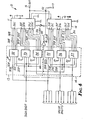
- FIG. 3 wherein is shown one embodiment of the digital to analog converter 10.
- a commercially available integrated circuit is used for each of the networks 11 and 12.
- This particular integrated circuit has a 12 bit capacity, however, depending upon the degree of accuracy which is required by this digital to analog converter 10, other networks having other capacities are equally viable.
- For a 12 bit capacity there are twelve inputs 30A through 30L or 31A through 31L.
- This embodiment also utilizes a plurality of identical integrated circuits for its circuits, designated generally 13 and 14. Each of these integrated circuits is a type SN 74LS157 data selector/multiplexer which is commercially available from Texas Instruments, Inc.
- each of these data selectors affords a 4-bit word to be selected from one of two inputs, and routed to a four terminal output.
- three data selectors must be utilized.
- the three data selectors for the first digital to analog network 11 are designated 32, 33 and 34.
- the three data selectors for the second digital to analog network 12 are designated 35, 36 and 37.
- each of these data selectors has two sets of four-bit inputs.
- the drawing only shows a single line representing the combination of the four-bit inputs. Therefore, in regar" to the first data selector 32, the first four bit input is designated 32A and the second four bit input is designated 32B.
- the three data selectors connected to their respective digital to analog networks 11 or 12 are identically configured. Therefore, a description is provided for only the first data selector (i.e. 32 or 35) within each group of three. This description will also apply to the other two data selectors which are connected to that particular digital to analog network 11 or 12.
- Each of the data selectors 32 and 35 contains two additional inputs designated 32C, 32D, and 35C, 35D respectively. These two inputs form part of the controller which is utilized to connect the alternative input sources to the corresponding digital to analog network 11 or 12.
- This particular integrated circuit has a function table which will select the A input when both the C input and the D input are low, and select the B input when the C input is low and the D input is high. When the C input is high, the resulting output of the data selectors will be a low voltage or a logic "zero".
- the A inputs i.e. 32A and 35A
- the B inputs i.e. 32B and 35B
- the reference voltage at 32A is sufficiently high to bring the network 11 to a logic "one" or on state.
- the reference voltage at 35A is sufficiently low, i.e., grounded, to bring the network 12 to a logic "zero" or off state.
- the third input 32C of the data selectors connected to the first network 11, is connected to the sign bit or sign digit of the incoming digital data, and the fourth input 32D is grounded, or brought to logic "zero".
- the third input 35C is connected to the inverse of the sign digit of the incoming digital signal, and the fourth input 35D is connected to a voltage source bringing it to a logic "zero" state.
- the logic scheme chosen to encode the digital data uses a sign digit of zero to indicate a positive signal, and a sign digit of one to indicate a negative signal. Therefore, if the incoming digital data corresponds to a positive analog signal, the sign bit will be zero causing the input 32C to be zero. Since the input 32D is grounded (logic zero), the input 32A will be selected and the input to the first digital to analog network 11 will be logic "ones". The inverse of the zero sign bit is fed to input 35C. Since input 35D is grounded, the source input 35B is chosen and the digital data is delivered to the second digital to analog network 12. Alternatively, if the sign bit is one, representing a negative analog signal, input 32C is high and again the input 32D is low.
- the input 32B is therefore chosen and the value digits of the digital data are delivered to the first digital to analog network 11.
- the input 35C however becomes a logic "zero" due to the inverse of the sign bit, resulting in a logic "zero” being inputted to the second digital to analog network 12.
- the first digital to analog network 11 is continuously on and the second digital to analog network 12 is progressively turned on as a function of the increasing signal value.
- the second digital to analog network 12 is turned off and the first digital to analog network is progressively turned off as a function of the digital signal becoming more negative.
- this phenomenon is illustrated by the transfer characteristics shown in Figure 2.
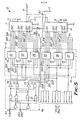
- FIG. 4 A variation of the present invention is shown in Figure 4. Again the same networks 11 and 12, and data selectors 32 through 37 are utilized. As before, the B inputs are reserved for the input of digital data, the 32A input is connected to a logic "one" reference voltage, input 32C is connected to the sign digit, and input 32 D is grounded. The A and the C inputs of the second set of data selectors, i.e., 35, 36, and 37, however, are both connected to a reference voltage sufficiently high to be a logic "one", and the sign digit is connected to the 35 D input. In this configuration a sign digit of zero will cause 32C to be low. Since 32D is also low, the 32A input will be chosen and logic "ones" will be fed to the first network 11.
- the sign digit will also be connected to input 35D. Hence for a negative signal input 35 D will be low. Since input 35C is always high, the input to the second digital to analog network 12 will be 35B, and the data will be fed to the second digital to analog network 12. For a negative signal the sign digit is 1. This results in put 32C being high. Since 32D is low, input 32B is chosen and the data is fed to the first network 11. The sign digit of one also causes input 35D to be high. Since input 35C is also high, logic zeros will be fed to the second network 12. Hence the result is the same as that described for Figure 3.
- Figure 5 illustrates a third embodiment of the present invention wherein a similar circuit as that already described is shown.
- the third embodiment contains additional circuitry which effectively serves to toggle or switch the two digital to analog networks 11 and 12 between their respective circuits 13 and 14. This toggling is done at a rate which is approximately one-half the sampling frequency which was originally used to create the digital data from its analog equivalent.
- This toggling of the digital to analog networks 11 and 12 is done to ensure that any discrepency between the two digital to analog networks 11 and 12, which might cause error or noise in the analog signal, will cause that noise or error at a known frequency, i.e. one-half the sampling frequency. This error or discrepancy can then be filtered out.
- a clock pulse is now added at terminal 45. This clock pulse has a frequency of one-half the sampling frequency as described.
- a configuration of NAND and NOT gates designated generally 46 form switches which in response to the sign digit and the clock pulse toggle the digital to analog networks 11 and 12.
- terminal 50 is the 32 D input
- terminal 51 the 32C input
- terminal 52 the 35D input
- terminal 53 the 35C input.
- the first network 11 toggles between the data and logic "ones” while the second network 12 toggles between logic "ones” and the data.
- the first network 11 toggles between logic "zeros” and data
- the second network toggles between the data and logic "zeros".
- this has the same transfer characteristic 20, but with the addition of the toggling function.
Abstract
Description
- This invention relates to digital to analog converters and in particular to bipolar converters having high accuracy at the zero crossover level.
- Digital to analog converters are designed to reconstruct complex and dynamic analog wave forms, particularly audio or acoustic signals, from digital data. When these signals are bipolar, i.e., operating both positively and negatively with respect to a zero crossover, the complexity required within the converter is greatly increased, usually with a loss in accuracy. In such signals, power occasionally peaks well above the RMS power level. There must, therefore, be a very large dynamic range to handle the bursts of higher amplitudes, as well as the ability to handle the wide range of frequency interest. Yet, accurately recreating such information from digital data requires exceptional small signal performance to handle the information near zero level or crossover without crossover distortion.
- In appreciation of this problem, digital to analog converters have been developed which separate the digital input signal into a polarity digit and a number of digits representing the absolute magnitude of the digital number, i.e., the magnitude excluding the polarity. When this is done, a unipolar digital to analog network can be used to convert the digital signal to its analog equivalent, and a switching or inverting/non-inverting amplifier can be used to restore the polarity to the signal once it has been converted, i.e., depending upon the polarity of the input signal, the output of the unipolar digital to analog network is either inverted or non-inverted. Although this circuit is able to improve the linearity of small signals in the center region of the full scale range, it requires a very accurate and costly inverting amplifier, and therefore tends to remain a limited solution.
- Another alternative has been to utilize two digital to analog networks, one of which operates from a positive reference source and the other of which operates from a negative reference source. Depending upon the polarity of the input signal as determined by the polarity digit, only one of the digital to analog networks is switched on, with its output being connected to a suitable operational amplifier. In this case only one or the other of the digital to analog converters is used at any given time, again to convert the absolute magnitude of the digital data, i.e., absent the polarity information. This circuit, however, requires that a positively operating digital to analog network be matched with a negatively operating digital to analog network. Since these two digital to analog networks are differently configured, it becomes increasingly difficult to find such a matched pair.
- The bipolar digital to analog converter of the present invention is able to provide relatively accurate conversion at the zero crossover point, as well as at higher magnitude levels without the need for a precise and costly operational amplifier, or matched pairs of positive and negative going digital to analog networks. This digital to analog converter does not require the digital data to be separated into a portion which corresponds to the absolute magnitude and a portion which corresponds to the polarity. Although the polarity or sign information must still be known in order to bias the converter, the converter of the present invention monitors the continuously changing relative value of the digital signal and proportionately changes its output signal in response thereto.
- The present invention comprises a pair of identically configured digital to analog networks, each having a plurality of input connections for the value digits of the digital data, and an output connection from which an analog signal corresponding to the digital data can be derived. The output connections of the two networks are electrically connected by an appropriate circuit to sum the output signals derived therefrom. The input connections of the two networks are also connected by an appropriate circuit. This circuit however is responsive to the polarity digit for directing the value digits to one or the other of the digital to analog networks. The circuit also establishes biasing states or biasing conditions for the networks, again in response to the polarity digit. In a first of these states or conditions, the digital to analog network not receiving the value digits is biased with a sufficiently high voltage, i.e., a logic "1" condition, to be completely turned on and therefore have a maximum output. The other digital to analog network, i.e., the one receiving data is then turned on or off progressively, as a function of the increase or decrease, respectively, in the relative value of the changing value digits. In a second biasing condition, the digital to analog network not receiving the data is biased with a sufficiently low or logic "0" voltage, to be completely turned off and therefore have a minimum or zero output. The other network, i.e., the one receiving the data, is then progressively turned off or on as a function of the decrease or increase, respectively, in the relative value of the changing value digits.
- If it is assumed that the first condition is responding to a sign digit indicating a positive signal and the second condition is responding to a negative signal, the converter of the present invention will have a maximum output for the most positive signal and a minimum of output for the most negative signal. Between these two extremes the output of the converter will be proportional to the actual value of the digital signal.
- The present invention will be further described hereinafter with reference to the accompanying drawing wherein:
- Figure 1 is a schematic diagram of the digital to analog converter of the present invention;
- Figure 2 is a graph of the transfer characteristics of the converter according to Figure 1;
- Figure 3 is a circuit diagram of a first embodiment of the converter according to Figure 1;
- Figure 4 is a circuit diagram of a second embodiment according to the present invention; and
- Figure 5 is a circuit diagram of a third embodiment according to the present invention.
- The
converter 10 according to the present invention is schematically illustrated in Figure 1. This converter comprises a pair of identically configured digital toanalog networks 11 and 12 respectively. Each of thesenetworks 11 or 12 has a plurality ofinput connections 30 and 31 (represented by a single line), respectively, for digital data, and anoutput connection input connections 30 electrically connected to afirst circuit 13 which is able to direct either aninput source 18 providing a logic "one", or the value digits of the digital data to the network 11. The second digital toanalog network 12 is electrically connected tosecond circuit 14 which directs either the value digits or aninput source 19 providing a logic "zero" to thenetwork 12. Control means 15, which are responsive to the sign digits of the digital data, determine which of the inputs are directed to the respective digital toanalog networks 11 and 12. The output signals of the two digital toanalog networks 11 and 12 are then summed, with the combined output signal being available atterminal 16. As will be discussed, the summing network also contains aterminal 17 at which a DC bias current can be added to change the relative DC position and shape of the resulting output signal. When thecircuits analog network 12 is responding to the changes in the value digits. The maximum output current is therefore flowing from the first digital to analog network 11. If the value digits are progressively increasing, the second digital toanalog network 12 would respond by progressively increasing its output current until it also is completely turned on, the condition at which theconverter 10 would have its maximum output. When the control means 15 switch the source of inputs, the value digits are fed to the first digital to analog network 11 and a low level or logic "zero" signal is fed to the inputs of the second digital toanalog network 12. In this condition, the second digital to analog network 12 i:: turned off, and the output current of the first digital to analog network 11 is responding to the changes in the value digits. If it is again assumed that the value digits are progressively increasing, the output current of the network 11 will increase progressively as a function of the increasingly value digits. If the value digits are, however, progressively decreasing, the network 11 will be progressively turned off until its output current, and the output of theconverter 10 as well, will be at a minimum value. - Assuming this to be a continuous process with the
controller 15 responding to a change in polarity of the digital signal, occurring at the time described, thetransfer characteristic 20 for the digital toanalog converting circuit 10 can be represented as shown in Figure 2. (Note - this graph shows the transfer characteristic without the addition of a bias current a;terminal 17 as will be discussed.) Theabscissa 21 of the graph shown represents the total output current of theconverter 10, and theordinate 22 represents the values of the digital data, separated into thesign digits 23 and the most significant three bits of thevalue digits 24. It should be noted that for a 12 bit converter, which is typical for the present circuit, there would be nine additional value digits (not shown) which form the input to theconverter 10. As can be seen from this graph, it is necessary to translate thetransfer characteristic 20 to the left by a distance equal to (I out max)/2 in order to make the output current bipolar and equally disposed about the ordinate 22. This can be done by adding a bias current at terminal 17 (see Figure 1). This bias current would be equal in magnitude to one half of the maximum total current which can be produced by the digital toanalog networks 11 and 12, but would, however, flow in the opposite direction as the output current flowing from the networks. With this addition, thetransfer characteristic 20 will be translated to the left by a distance equal to this bias current atterminal 17. The zero crossover of the output current would then occur during a transition of the digital input signal between 0 000 and 1 111. As can also be seen from thistransfer characteristic 20, substantially the same output current is present for the digital values of 0 000 and 1 111. (Note - this situation is exaggerated since only the three most significant value digits out of the total twelve value digits are shown.) This substantial equality of the current levels exists because at both levels one digital to analog network is approaching being completely turned on and the other network is approaching being completely turned off (Note - if all digits were shown, an interval would exist where one network would be fully on, and the other fully off). In order to make the transfer characteristic linear it is necessary to also add a bias current to the output current of eachnetwork 11 and 12 whenever the digital data is positive, i.e., thesign digit 23 is zero. This bias current should be equal in value to the change in output current which occurs for a change in the value of the least significant digit, i.e., the twelfth digit. In the preferred embodiment this is done by connecting an appropriate (see Fig. 3)resistor 40 betweenterminals sign digit 23 becomes zero, terminal 41 is high, and a current will flow through theresistor 40. The addition of the two bias currents explained above will result in a linear transfer curve which is symmetric about theordinate 22. - The operation of the present invention is best described by reference to Figure 3 wherein is shown one embodiment of the digital to
analog converter 10. A commercially available integrated circuit is used for each of thenetworks 11 and 12. This particular integrated circuit has a 12 bit capacity, however, depending upon the degree of accuracy which is required by this digital toanalog converter 10, other networks having other capacities are equally viable. For a 12 bit capacity there are twelveinputs 30A through 30L or 31A through 31L. This embodiment also utilizes a plurality of identical integrated circuits for its circuits, designated generally 13 and 14. Each of these integrated circuits is a type SN 74LS157 data selector/multiplexer which is commercially available from Texas Instruments, Inc. These data selectors afford a 4-bit word to be selected from one of two inputs, and routed to a four terminal output. Thus, for a 12-bit digital to analog network, three data selectors must be utilized. The three data selectors for the first digital to analog network 11 are designated 32, 33 and 34. Similarly, the three data selectors for the second digital toanalog network 12 are designated 35, 36 and 37. As has already been indicated, each of these data selectors has two sets of four-bit inputs. For the sake of simplicity, the drawing only shows a single line representing the combination of the four-bit inputs. Therefore, in regar" to thefirst data selector 32, the first four bit input is designated 32A and the second four bit input is designated 32B. This same identification scheme is also true for the remainder of the data selectors. The three data selectors connected to their respective digital toanalog networks 11 or 12 are identically configured. Therefore, a description is provided for only the first data selector (i.e. 32 or 35) within each group of three. This description will also apply to the other two data selectors which are connected to that particular digital toanalog network 11 or 12. Each of thedata selectors analog network 11 or 12. This particular integrated circuit has a function table which will select the A input when both the C input and the D input are low, and select the B input when the C input is low and the D input is high. When the C input is high, the resulting output of the data selectors will be a low voltage or a logic "zero". - The A inputs, i.e. 32A and 35A, are connected to a source which supplies a pre-determined reference voltage, and the B inputs, i.e. 32B and 35B, are the inputs for the twelve data bits, or value digits which are present in the incoming digital data to being converted. For the embodiment shown in Figure 3, the reference voltage at 32A is sufficiently high to bring the network 11 to a logic "one" or on state. Contrastingly, the reference voltage at 35A is sufficiently low, i.e., grounded, to bring the
network 12 to a logic "zero" or off state. The third input 32C of the data selectors connected to the first network 11, is connected to the sign bit or sign digit of the incoming digital data, and thefourth input 32D is grounded, or brought to logic "zero". For the data selectors connected to the second digital toanalog network 12, the third input 35C is connected to the inverse of the sign digit of the incoming digital signal, and the fourth input 35D is connected to a voltage source bringing it to a logic "zero" state. - The logic scheme chosen to encode the digital data, uses a sign digit of zero to indicate a positive signal, and a sign digit of one to indicate a negative signal. Therefore, if the incoming digital data corresponds to a positive analog signal, the sign bit will be zero causing the input 32C to be zero. Since the
input 32D is grounded (logic zero), theinput 32A will be selected and the input to the first digital to analog network 11 will be logic "ones". The inverse of the zero sign bit is fed to input 35C. Since input 35D is grounded, thesource input 35B is chosen and the digital data is delivered to the second digital toanalog network 12. Alternatively, if the sign bit is one, representing a negative analog signal, input 32C is high and again theinput 32D is low. Theinput 32B is therefore chosen and the value digits of the digital data are delivered to the first digital to analog network 11. The input 35C however becomes a logic "zero" due to the inverse of the sign bit, resulting in a logic "zero" being inputted to the second digital toanalog network 12. Thus, for positive signals, the first digital to analog network 11 is continuously on and the second digital toanalog network 12 is progressively turned on as a function of the increasing signal value. For negative signals, however, the second digital toanalog network 12 is turned off and the first digital to analog network is progressively turned off as a function of the digital signal becoming more negative. As has already been described, this phenomenon is illustrated by the transfer characteristics shown in Figure 2. - A variation of the present invention is shown in Figure 4. Again the
same networks 11 and 12, anddata selectors 32 through 37 are utilized. As before, the B inputs are reserved for the input of digital data, the 32A input is connected to a logic "one" reference voltage, input 32C is connected to the sign digit, andinput 32D is grounded. The A and the C inputs of the second set of data selectors, i.e., 35, 36, and 37, however, are both connected to a reference voltage sufficiently high to be a logic "one", and the sign digit is connected to the 35D input. In this configuration a sign digit of zero will cause 32C to be low. Since 32D is also low, the 32A input will be chosen and logic "ones" will be fed to the first network 11. The sign digit will also be connected to input 35D. Hence for anegative signal input 35D will be low. Since input 35C is always high, the input to the second digital toanalog network 12 will be 35B, and the data will be fed to the second digital toanalog network 12. For a negative signal the sign digit is 1. This results in put 32C being high. Since 32D is low,input 32B is chosen and the data is fed to the first network 11. The sign digit of one also causes input 35D to be high. Since input 35C is also high, logic zeros will be fed to thesecond network 12. Hence the result is the same as that described for Figure 3. - Although the present invention improves the ability of the digital to analog networks to convert the zero crossover information, there is still a concern for minor variations which might occur, e.g. even in the same manufacturing lot of networks, therefore Figure 5 illustrates a third embodiment of the present invention wherein a similar circuit as that already described is shown. The third embodiment, however, contains additional circuitry which effectively serves to toggle or switch the two digital to
analog networks 11 and 12 between theirrespective circuits analog networks 11 and 12 is done to ensure that any discrepency between the two digital toanalog networks 11 and 12, which might cause error or noise in the analog signal, will cause that noise or error at a known frequency, i.e. one-half the sampling frequency. This error or discrepancy can then be filtered out. For this purpose, a clock pulse is now added at terminal 45. This clock pulse has a frequency of one-half the sampling frequency as described. A configuration of NAND and NOT gates designated generally 46 form switches which in response to the sign digit and the clock pulse toggle the digital toanalog networks 11 and 12. The actual conditions which are obtained by the gates for the various clock and sign bit conditions are indicated in the following table:
embodiment terminal 50 is the 32D input, terminal 51 the 32C input, terminal 52 the 35D input, and terminal 53 the 35C input. Thus for a positive signal the first network 11 toggles between the data and logic "ones" while thesecond network 12 toggles between logic "ones" and the data. For a negative signal, however, the first network 11 toggles between logic "zeros" and data, while the second network toggles between the data and logic "zeros". As can be seen, this has the same transfer characteristic 20, but with the addition of the toggling function. - Having thus described several embodiments of the present invention, it will be understood that changes may be made in the size, shape and configuration of some of the parts or circuits described herein without departing. from the present invention as recited in the appended claims.
Claims (7)
Applications Claiming Priority (2)
| Application Number | Priority Date | Filing Date | Title |
|---|---|---|---|
| US320546 | 1981-11-12 | ||
| US06/320,546 US4473818A (en) | 1981-11-12 | 1981-11-12 | Bipolar digital to analog converter |
Publications (3)
| Publication Number | Publication Date |
|---|---|
| EP0079681A2 true EP0079681A2 (en) | 1983-05-25 |
| EP0079681A3 EP0079681A3 (en) | 1986-03-19 |
| EP0079681B1 EP0079681B1 (en) | 1990-08-08 |
Family
ID=23246908
Family Applications (1)
| Application Number | Title | Priority Date | Filing Date |
|---|---|---|---|
| EP82305443A Expired - Lifetime EP0079681B1 (en) | 1981-11-12 | 1982-10-13 | Bipolar digital to analog converter |
Country Status (6)
| Country | Link |
|---|---|
| US (1) | US4473818A (en) |
| EP (1) | EP0079681B1 (en) |
| JP (1) | JPS5888923A (en) |
| AU (1) | AU555038B2 (en) |
| CA (1) | CA1188810A (en) |
| DE (1) | DE3280225D1 (en) |
Cited By (2)
| Publication number | Priority date | Publication date | Assignee | Title |
|---|---|---|---|---|
| EP0287312A2 (en) * | 1987-04-13 | 1988-10-19 | Matsushita Electric Industrial Co., Ltd. | Digital-analog converter |
| US4973979A (en) * | 1987-12-21 | 1990-11-27 | Nissan Motor Company, Limited | Circuit and method for converting digital signal into corresponding analog signal |
Families Citing this family (5)
| Publication number | Priority date | Publication date | Assignee | Title |
|---|---|---|---|---|
| US4791405A (en) * | 1986-11-28 | 1988-12-13 | Motorola, Inc. | Data converter for directly providing outputs in two's complement code |
| US5257027A (en) * | 1992-07-20 | 1993-10-26 | Burr-Brown Corporation | Modified sign-magnitude DAC and method |
| US5689259A (en) * | 1995-07-21 | 1997-11-18 | Exar Corporation | Differental D/A converter with N-bits plus sign |
| US6639534B2 (en) * | 2002-02-14 | 2003-10-28 | Silicon Laboratories, Inc. | Digital-to-analog converter switching circuitry |
| WO2015021337A1 (en) * | 2013-08-07 | 2015-02-12 | Xagenic Inc. | Precision bipolar current-mode-digital-to-analog converter |
Citations (4)
| Publication number | Priority date | Publication date | Assignee | Title |
|---|---|---|---|---|
| US2878434A (en) * | 1954-05-10 | 1959-03-17 | North American Aviation Inc | Error sensing servo component |
| US3582941A (en) * | 1966-11-28 | 1971-06-01 | Int Standard Electric Corp | Nonlinear decoder |
| US3810157A (en) * | 1972-02-14 | 1974-05-07 | Sperry Rand Corp | Bipolar digital-to-analog converter |
| FR2449367A1 (en) * | 1979-02-15 | 1980-09-12 | Microsystemes Sarl | A=D signal converter - has weighted outputs of several low resolution converters summed to provide high resolution output |
Family Cites Families (5)
| Publication number | Priority date | Publication date | Assignee | Title |
|---|---|---|---|---|
| DE1287622B (en) * | 1964-12-24 | 1969-01-23 | ||
| US3582939A (en) * | 1969-09-19 | 1971-06-01 | Honeywell Inc | Bipolar digital-to-analog converter |
| US3877023A (en) * | 1973-05-21 | 1975-04-08 | Texas Instruments Inc | Antiglitch digital to analog converter system |
| JPS5327353A (en) * | 1976-08-27 | 1978-03-14 | Fujitsu Ltd | Bipolar digital-analog converter |
| US4346368A (en) * | 1979-11-23 | 1982-08-24 | The Boeing Company | Digital-to-analog converter capable of processing a sign magnitude or ones complement binary coded input |
-
1981
- 1981-11-12 US US06/320,546 patent/US4473818A/en not_active Expired - Fee Related
-
1982
- 1982-10-05 CA CA000412834A patent/CA1188810A/en not_active Expired
- 1982-10-13 DE DE8282305443T patent/DE3280225D1/en not_active Expired - Fee Related
- 1982-10-13 EP EP82305443A patent/EP0079681B1/en not_active Expired - Lifetime
- 1982-11-11 JP JP57196888A patent/JPS5888923A/en active Pending
- 1982-11-11 AU AU90363/82A patent/AU555038B2/en not_active Ceased
Patent Citations (4)
| Publication number | Priority date | Publication date | Assignee | Title |
|---|---|---|---|---|
| US2878434A (en) * | 1954-05-10 | 1959-03-17 | North American Aviation Inc | Error sensing servo component |
| US3582941A (en) * | 1966-11-28 | 1971-06-01 | Int Standard Electric Corp | Nonlinear decoder |
| US3810157A (en) * | 1972-02-14 | 1974-05-07 | Sperry Rand Corp | Bipolar digital-to-analog converter |
| FR2449367A1 (en) * | 1979-02-15 | 1980-09-12 | Microsystemes Sarl | A=D signal converter - has weighted outputs of several low resolution converters summed to provide high resolution output |
Cited By (3)
| Publication number | Priority date | Publication date | Assignee | Title |
|---|---|---|---|---|
| EP0287312A2 (en) * | 1987-04-13 | 1988-10-19 | Matsushita Electric Industrial Co., Ltd. | Digital-analog converter |
| EP0287312A3 (en) * | 1987-04-13 | 1992-05-13 | Matsushita Electric Industrial Co., Ltd. | Digital-analog converter |
| US4973979A (en) * | 1987-12-21 | 1990-11-27 | Nissan Motor Company, Limited | Circuit and method for converting digital signal into corresponding analog signal |
Also Published As
| Publication number | Publication date |
|---|---|
| CA1188810A (en) | 1985-06-11 |
| US4473818A (en) | 1984-09-25 |
| EP0079681B1 (en) | 1990-08-08 |
| JPS5888923A (en) | 1983-05-27 |
| EP0079681A3 (en) | 1986-03-19 |
| DE3280225D1 (en) | 1990-09-13 |
| AU9036382A (en) | 1983-05-19 |
| AU555038B2 (en) | 1986-09-11 |
Similar Documents
| Publication | Publication Date | Title |
|---|---|---|
| US3997892A (en) | Digital to analog converter with improved companding | |
| US4751497A (en) | Digital to analog converter with high output compliance | |
| US3217147A (en) | Cumulative type decoder | |
| US4275386A (en) | Binary analog-digital converter | |
| US4636772A (en) | Multiple function type D/A converter | |
| US5619203A (en) | Current source driven converter | |
| CA1144653A (en) | Codec | |
| US4473818A (en) | Bipolar digital to analog converter | |
| JPH02228818A (en) | Digital/analog converter having single-resistor row having transferable potential | |
| US3582939A (en) | Bipolar digital-to-analog converter | |
| US3789389A (en) | Method and circuit for combining digital and analog signals | |
| US4567463A (en) | Circuit for improving the performance of digital to analog converters | |
| US3396380A (en) | Digital-analogue signal converter | |
| US3568147A (en) | Transient filter system | |
| US4857929A (en) | Apparatus for converting data between analog and digital values | |
| EP0214703B1 (en) | Analog-to-digital converter circuit | |
| US4225816A (en) | Precision current source | |
| EP0095674B1 (en) | Apparatus for converting data between analog and digital values | |
| US4851846A (en) | Apparatus for converting an analog balanced signal to a digital signal | |
| JPH0621814A (en) | Digital-to-analog converter provided with precise linear output for both positive and negative input values | |
| US3810157A (en) | Bipolar digital-to-analog converter | |
| EP0074860A3 (en) | Digital-to-analog converter | |
| US4124824A (en) | Voltage subtractor for serial-parallel analog-to-digital converter | |
| US20040125004A1 (en) | D/A converter for converting plurality of digital signals simultaneously | |
| US4336527A (en) | Digital-to-analog converter |
Legal Events
| Date | Code | Title | Description |
|---|---|---|---|
| PUAI | Public reference made under article 153(3) epc to a published international application that has entered the european phase |
Free format text: ORIGINAL CODE: 0009012 |
|
| AK | Designated contracting states |
Designated state(s): DE FR GB IT |
|
| PUAL | Search report despatched |
Free format text: ORIGINAL CODE: 0009013 |
|
| AK | Designated contracting states |
Kind code of ref document: A3 Designated state(s): DE FR GB IT |
|
| 17P | Request for examination filed |
Effective date: 19860915 |
|
| 17Q | First examination report despatched |
Effective date: 19871028 |
|
| ITF | It: translation for a ep patent filed |
Owner name: BARZANO' E ZANARDO ROMA S.P.A. |
|
| GRAA | (expected) grant |
Free format text: ORIGINAL CODE: 0009210 |
|
| AK | Designated contracting states |
Kind code of ref document: B1 Designated state(s): DE FR GB IT |
|
| REF | Corresponds to: |
Ref document number: 3280225 Country of ref document: DE Date of ref document: 19900913 |
|
| ET | Fr: translation filed | ||
| PG25 | Lapsed in a contracting state [announced via postgrant information from national office to epo] |
Ref country code: GB Effective date: 19901013 |
|
| PLBE | No opposition filed within time limit |
Free format text: ORIGINAL CODE: 0009261 |
|
| STAA | Information on the status of an ep patent application or granted ep patent |
Free format text: STATUS: NO OPPOSITION FILED WITHIN TIME LIMIT |
|
| GBPC | Gb: european patent ceased through non-payment of renewal fee | ||
| PG25 | Lapsed in a contracting state [announced via postgrant information from national office to epo] |
Ref country code: FR Effective date: 19910628 |
|
| PG25 | Lapsed in a contracting state [announced via postgrant information from national office to epo] |
Ref country code: DE Effective date: 19910702 |
|
| 26N | No opposition filed | ||
| REG | Reference to a national code |
Ref country code: FR Ref legal event code: ST |