EP0083986A2 - Polychromatic image sensor - Google Patents
Polychromatic image sensor Download PDFInfo
- Publication number
- EP0083986A2 EP0083986A2 EP83300113A EP83300113A EP0083986A2 EP 0083986 A2 EP0083986 A2 EP 0083986A2 EP 83300113 A EP83300113 A EP 83300113A EP 83300113 A EP83300113 A EP 83300113A EP 0083986 A2 EP0083986 A2 EP 0083986A2
- Authority
- EP
- European Patent Office
- Prior art keywords
- light
- junctions
- sensor
- region
- receiving surface
- Prior art date
- Legal status (The legal status is an assumption and is not a legal conclusion. Google has not performed a legal analysis and makes no representation as to the accuracy of the status listed.)
- Ceased
Links
- VYPSYNLAJGMNEJ-UHFFFAOYSA-N Silicium dioxide Chemical compound O=[Si]=O VYPSYNLAJGMNEJ-UHFFFAOYSA-N 0.000 claims abstract description 16
- 239000004065 semiconductor Substances 0.000 claims abstract description 13
- 230000003287 optical effect Effects 0.000 claims description 5
- 238000009826 distribution Methods 0.000 claims description 3
- 235000012239 silicon dioxide Nutrition 0.000 claims 1
- 239000000377 silicon dioxide Substances 0.000 claims 1
- 229910052814 silicon oxide Inorganic materials 0.000 abstract description 12
- 230000035515 penetration Effects 0.000 abstract description 2
- 239000000463 material Substances 0.000 abstract 2
- XUIMIQQOPSSXEZ-UHFFFAOYSA-N Silicon Chemical compound [Si] XUIMIQQOPSSXEZ-UHFFFAOYSA-N 0.000 description 5
- 229910052710 silicon Inorganic materials 0.000 description 5
- 239000010703 silicon Substances 0.000 description 5
- 230000035945 sensitivity Effects 0.000 description 4
- 239000004020 conductor Substances 0.000 description 3
- 238000010586 diagram Methods 0.000 description 3
- 238000010521 absorption reaction Methods 0.000 description 2
- 238000009792 diffusion process Methods 0.000 description 2
- 238000000926 separation method Methods 0.000 description 2
- 238000006243 chemical reaction Methods 0.000 description 1
- 239000011248 coating agent Substances 0.000 description 1
- 238000000576 coating method Methods 0.000 description 1
- 239000003086 colorant Substances 0.000 description 1
- 230000007423 decrease Effects 0.000 description 1
- 238000004519 manufacturing process Methods 0.000 description 1
Images


Classifications
-
- H—ELECTRICITY
- H01—ELECTRIC ELEMENTS
- H01L—SEMICONDUCTOR DEVICES NOT COVERED BY CLASS H10
- H01L27/00—Devices consisting of a plurality of semiconductor or other solid-state components formed in or on a common substrate
- H01L27/14—Devices consisting of a plurality of semiconductor or other solid-state components formed in or on a common substrate including semiconductor components sensitive to infrared radiation, light, electromagnetic radiation of shorter wavelength or corpuscular radiation and specially adapted either for the conversion of the energy of such radiation into electrical energy or for the control of electrical energy by such radiation
- H01L27/144—Devices controlled by radiation
- H01L27/146—Imager structures
- H01L27/14643—Photodiode arrays; MOS imagers
- H01L27/14645—Colour imagers
-
- H—ELECTRICITY
- H01—ELECTRIC ELEMENTS
- H01L—SEMICONDUCTOR DEVICES NOT COVERED BY CLASS H10
- H01L31/00—Semiconductor devices sensitive to infrared radiation, light, electromagnetic radiation of shorter wavelength or corpuscular radiation and specially adapted either for the conversion of the energy of such radiation into electrical energy or for the control of electrical energy by such radiation; Processes or apparatus specially adapted for the manufacture or treatment thereof or of parts thereof; Details thereof
- H01L31/08—Semiconductor devices sensitive to infrared radiation, light, electromagnetic radiation of shorter wavelength or corpuscular radiation and specially adapted either for the conversion of the energy of such radiation into electrical energy or for the control of electrical energy by such radiation; Processes or apparatus specially adapted for the manufacture or treatment thereof or of parts thereof; Details thereof in which radiation controls flow of current through the device, e.g. photoresistors
- H01L31/10—Semiconductor devices sensitive to infrared radiation, light, electromagnetic radiation of shorter wavelength or corpuscular radiation and specially adapted either for the conversion of the energy of such radiation into electrical energy or for the control of electrical energy by such radiation; Processes or apparatus specially adapted for the manufacture or treatment thereof or of parts thereof; Details thereof in which radiation controls flow of current through the device, e.g. photoresistors characterised by at least one potential-jump barrier or surface barrier, e.g. phototransistors
- H01L31/101—Devices sensitive to infrared, visible or ultraviolet radiation
- H01L31/111—Devices sensitive to infrared, visible or ultraviolet radiation characterised by at least three potential barriers, e.g. photothyristor
Definitions
- This invention relates to a photoelectric conversion element or image sensor used for an original document reading apparatus such as a facsimile system.
- the invention relates to a polychromatic image sensor having colour separation and reading capability for two or more colours.
- FIG. 1 of the accompanying drawings illustrates a conventional polychromatic image sensor of the type mentioned above, which is composed of a film 1 of silicon oxide (Si0 2 ), a P-type diffusion region 2 (hereinafter referred to as a P-region), an N-type diffusion region 3 (hereinafter referred to as an N-region), and a second P-region 4. Electrode lead conductors 5, 6 and 7 are respectively led out from the P-region 2, the N-region 3 and the P-region 4.
- Reference numerals 8 and 9 denote first and second PN-junctions, respectively.
- Figure 2 of the accompanying drawings is an equivalent circuit diagram of the polychromatic image sensor shown in Figure 1, wherein a photodiode 10 is defined by the P-region 2 and the N-region 3, and a photodiode 11 is defined by the N-region 3 and the P-region 4.
- the electrode lead conductor 6 is coupled to the junction between the respective cathodes of the photodiodes 10 and 11, while the electrode lead conductors 5 and 7 are led out from the anodes of the photodiodes 10 and 11, respectively.
- the polychromatic image sensor of Figure 1 may have colour separation.and reading capability, because when light of various frequencies impinges the silicon, the coefficient of absorption varies in the manner shown graphically in Figure 3 of the accompanying drawings. Consequently, there is a known relationship between wavelength of the light and the absorption into the silicon.
- Figure 4 of the accompanying drawings is a graph showing for various wavelengths ( ⁇ ) the percentage of light quanta which penetrate a distance x into the silicon from the light-receiving surface of the latter. From Figures 3 and 4 it will be appreciated that, as the wavelength of the light decreases, the silicon absorbs light more effectively and that conversely, as the wavelength becomes longer, the greater the penetration into the silicon. Accordingly, it will be apparent from the configuration of the polychromatic image sensor that the first PN-junction 8 can be reached by light of short wavelengths as well as light of long wavelengths, while the second PN-junction 9 cannot generally be reached by short wavelength light, which will have been absorbed in the regions 2 and 3. Accordingly, information which includes short wavelength light can be obtained from the first photodiode 10, while information which excludes short wavelength light can be obtained from the second photodiode 11.
- the present invention provides a polychromatic semiconductor image sensor for converting an optical signal into an electrical signal, comprising a light-receiving surface, a region of a first semiconductor type formed below said light- receiving surface, and a plurality of regions of a second semiconductor type disposed relative to the first-mentioned region to define at least two PN-junctions, wherein the distance of the PN-junctions from the light-receiving surface varies continuously across or along the latter.
- a plurality of such sensors may be arrayed.
- a first embodiment of the present invention is shown in Figures 6A and 6B, wherein the sensor comprises a film 20 of silicon oxide (Si0 2 ), a P-region 21, first and second N-regions 22 and 23 respectively, first to third electrodes 24 to 26 respectively, and first and second PN-junctions 27 and 28 respectively.
- the equivalent electrical circuit is shown in Figure 7, wherein a first photodiode 29 is defined by the P-region 21 and the N-region 22 and a second photodiode 30 is defined by the P-region 21 and the N -region 23.
- the distance between the silicon oxide film 20 and the first PN-junction 27 is different from that between the silicon oxide film 20 and the second PN-junction 28. Accordingly, if light of differing wavelengths falls on the silicon oxide film, the wavelength distribution of the light which reaches the first PN-junction 27 will be different from that of the light whih reaches the second PN-junction 28. Consequently, the first and second photodiodes 29 and 30 differ from each other in relative sensitivity to the wavelengths, so that characteristics approximating to those shown in Figure 5 can be obtained.
- the length l (being the dimension of the P-region 21 in a plane parallel to the film 20) selected to be 10 ⁇ m to 20 um.
- the optical information is first compressed through an optical system, for example by a factor 0.2, and is then supplied to the polychromatic image sensor. This means, accordingly, that the information over a dimension of 50 ⁇ m to 100 um on the original document is inputted into the polychromatic image sensor.
- the first and second PN-junctions 27 and 29 are laterally shifted, such a shift is effectively irrelevant because only a very small area of the document will be inputted to the polychromatic image sensor.
- Figures 8 and 9 illustrate a second embodiment of the present invention, wherein the sensor comprises a film 20 of silicon oxide, a P-region 31, first to third N-regions 32 to 34 respectively, electrodes 35 to 38, a first PN-junction 39 and second PN-junctions 40 ' and 41.
- the sensor comprises a film 20 of silicon oxide, a P-region 31, first to third N-regions 32 to 34 respectively, electrodes 35 to 38, a first PN-junction 39 and second PN-junctions 40 ' and 41.
- the boundaries between the P-region and the N-regions extend in a straight line.
- the sensor of this-embodiment functions in a similar manner to the first embodiment, because the distance between the silicon oxide film 20 and the first PN-junction 39 is different from that between the silicon oxide film 20 and the second PN-junctions 40,41. However, the distance does not vary linearly as in the first embodiment, but rather varies continuously as a function of the radius of curvature defining the boundary of the P-region 31.
- Figure 10 illustrates a third embodiment of the present invention which differs from the embodiment shown in Figures 6A and 6B in that four N-regions are provided, these being referenced 42 to 45 respectively.
- Reference numerals 46 to 49 designate respective electrodes for these N-regions.
- each of the above-described embodiments of the invention has an advantage over conventional polychromatic image sensors, in that the distance from the silicon oxide film to the PN-junction does not have to be formed with a high degree of accuracy, since this distance gradually and continuously varies. Hence, strict coating tolerances in manufacture are not needed. There is a further advantage in that more than two PN-junctions can be easily made (for example as shown in Figure 10) so that light having various wavelength distributions can be converted into electrical signals.
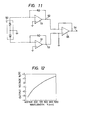
- Figure 11 illustrates a circuit for processing electrical signals derived from a polychromatic image sensor according to the present invention.
- the sensor shown in Figures 6A and 6B is utilised in Figure 11, being referenced 50.
- the output electrodes of the sensor 50 are each connected to the inverting input of a respective operational amplifier 51, the non-inverting input thereof being earthed.
- Each amplifier 51 has a diode connected in its feedback circuit.
- Output terminals 52 and 53 of the two amplifiers 51 are connected respectively to the inputs of a further operational amplifier 55, the latter having an output terminal 54.
- Light intensity information can be obtained from the terminals 52 and 53 as outputs from the respective diodes.
- an output voltage Vo which is a function of colour (i.e. colour information) can be obtained at the terminal 54.
- Figure 12 is a graph showing the relationship between the output voltage Vo and the wavelength of the light incident on the sensor 50.
Landscapes
- Physics & Mathematics (AREA)
- Engineering & Computer Science (AREA)
- Power Engineering (AREA)
- Electromagnetism (AREA)
- Condensed Matter Physics & Semiconductors (AREA)
- General Physics & Mathematics (AREA)
- Computer Hardware Design (AREA)
- Microelectronics & Electronic Packaging (AREA)
- Solid State Image Pick-Up Elements (AREA)
- Light Receiving Elements (AREA)
- Facsimile Heads (AREA)
Abstract
Description
- This invention relates to a photoelectric conversion element or image sensor used for an original document reading apparatus such as a facsimile system. In particular, the invention relates to a polychromatic image sensor having colour separation and reading capability for two or more colours.
- Figure 1 of the accompanying drawings illustrates a conventional polychromatic image sensor of the type mentioned above, which is composed of a
film 1 of silicon oxide (Si02), a P-type diffusion region 2 (hereinafter referred to as a P-region), an N-type diffusion region 3 (hereinafter referred to as an N-region), and a second P-region 4.Electrode lead conductors region 2, the N-region 3 and the P-region 4.Reference numerals - Figure 2 of the accompanying drawings is an equivalent circuit diagram of the polychromatic image sensor shown in Figure 1, wherein a
photodiode 10 is defined by the P-region 2 and the N-region 3, and a photodiode 11 is defined by the N-region 3 and the P-region 4. Theelectrode lead conductor 6 is coupled to the junction between the respective cathodes of thephotodiodes 10 and 11, while theelectrode lead conductors photodiodes 10 and 11, respectively. - The polychromatic image sensor of Figure 1 may have colour separation.and reading capability, because when light of various frequencies impinges the silicon, the coefficient of absorption varies in the manner shown graphically in Figure 3 of the accompanying drawings. Consequently, there is a known relationship between wavelength of the light and the absorption into the silicon.
- Figure 4 of the accompanying drawings is a graph showing for various wavelengths (À) the percentage of light quanta which penetrate a distance x into the silicon from the light-receiving surface of the latter. From Figures 3 and 4 it will be appreciated that, as the wavelength of the light decreases, the silicon absorbs light more effectively and that conversely, as the wavelength becomes longer, the greater the penetration into the silicon. Accordingly, it will be apparent from the configuration of the polychromatic image sensor that the first PN-
junction 8 can be reached by light of short wavelengths as well as light of long wavelengths, while the second PN-junction 9 cannot generally be reached by short wavelength light, which will have been absorbed in theregions first photodiode 10, while information which excludes short wavelength light can be obtained from the second photodiode 11. - Characteristics as shown in -Figure 5 of the accompanying drawings have been reported as obtained in the polychromatic image sensor shown in Figure 1. In Figure 5,
curves 10a and lla denote the characteristics of the first andsecond photodiodes 10 and 11, respectively. It will be seen from these characteristics that thefirst photodiode 10 has high sensitivity to short wavelength light and, on the contrary, the second photodiode 11 has high sensitivity to long wavelength light. - There is however a drawback in the polychromatic image sensor shown in Figure 1, in that the first and second PN-
junctions silicon oxide film 1. More specifically, in order to obtain a polychromatic image sensor having the desired characteristics, it is necessary to form with precision the distance from the silicon oxide film to each of the first and second PN-junction planes, which is rather difficult. Moreover, it is also difficult to produce two or more PN-junctions accurately. - It is an object of the present invention to eliminate the above-described drawbacks of conventional polychromatic image sensors, and to provide a polychromatic image sensor in which the desired characteristics can be easily obtained and in which two or more PN-junctions can easily and accurately be produced.
- Accordingly, the present invention provides a polychromatic semiconductor image sensor for converting an optical signal into an electrical signal, comprising a light-receiving surface, a region of a first semiconductor type formed below said light- receiving surface, and a plurality of regions of a second semiconductor type disposed relative to the first-mentioned region to define at least two PN-junctions, wherein the distance of the PN-junctions from the light-receiving surface varies continuously across or along the latter.
- In a preferred aspect of the invention, a plurality of such sensors may be arrayed.
- The invention will now be further described, by way of example only, with reference to the remaining Figures of the accompanying drawings, in which:-
- Figure 6A is a plan view of a first embodiment of a sensor according to the present invention;
- Figure 6B is a cross-sectional view taken along the line A-A' in Figure 6A;
- Figure 7 is a diagram illustrating a circuit equivalent to the sensor shown in Figures 6A and 6B;
- Figure 8 is a cross-sectional view of a second embodiment of a sensor according to the present invention;
- Figure 9 is an underneath plan view of the sensor shown in Figure 8;
- Figure 10 is a cross-sectional view of a third embodiment of a sensor according to the present invention;
- Figure 11 is a diagram of a signal processing circuit to which a polychromatic image sensor according to the invention may be applied; and
- Figure 12 is a graph showing the relationship between an output voltage of the circuit shown in Figure 11 and the wavelength of the light incident on the sensor, for explaining the chromatic or colour information which can be obtained from the circuit of Figure 11.
- A first embodiment of the present invention is shown in Figures 6A and 6B, wherein the sensor comprises a
film 20 of silicon oxide (Si02), a P-region 21, first and second N-regions third electrodes 24 to 26 respectively, and first and second PN-junctions first photodiode 29 is defined by the P-region 21 and the N-region 22 and asecond photodiode 30 is defined by the P-region 21 and the N-region 23. - In the thus arranged polychromatic image sensor, as is apparent from Figure 6B, the distance between the
silicon oxide film 20 and the first PN-junction 27 is different from that between thesilicon oxide film 20 and the second PN-junction 28. Accordingly, if light of differing wavelengths falls on the silicon oxide film, the wavelength distribution of the light which reaches the first PN-junction 27 will be different from that of the light whih reaches the second PN-junction 28. Consequently, the first andsecond photodiodes - The reason why such sensitivity can be obtained has been already described, and will therefore not be repeated here.
- In producing the polychromatic image sensor described above; the length ℓ (being the dimension of the P-
region 21 in a plane parallel to the film 20) selected to be 10 µm to 20 um. In order to convert optical information from an original document into an electrical signal, the optical information is first compressed through an optical system, for example by a factor 0.2, and is then supplied to the polychromatic image sensor. This means, accordingly, that the information over a dimension of 50 µm to 100 um on the original document is inputted into the polychromatic image sensor. Although the first and second PN-junctions - Figures 8 and 9 illustrate a second embodiment of the present invention, wherein the sensor comprises a
film 20 of silicon oxide, a P-region 31, first to third N-regions 32 to 34 respectively,electrodes 35 to 38, a first PN-junction 39 and second PN-junctions - The sensor of this-embodiment functions in a similar manner to the first embodiment, because the distance between the
silicon oxide film 20 and the first PN-junction 39 is different from that between thesilicon oxide film 20 and the second PN-junctions region 31. - Figure 10 illustrates a third embodiment of the present invention which differs from the embodiment shown in Figures 6A and 6B in that four N-regions are provided, these being referenced 42 to 45 respectively.
Reference numerals 46 to 49 designate respective electrodes for these N-regions. By increasing the number of N-regions and corresponding electrodes, the equivalent circuit will have a corresponding increased number of parallel branches. It will be appreciated that the number of N-regions may be varied still further. - Each of the above-described embodiments of the invention has an advantage over conventional polychromatic image sensors, in that the distance from the silicon oxide film to the PN-junction does not have to be formed with a high degree of accuracy, since this distance gradually and continuously varies. Hence, strict coating tolerances in manufacture are not needed. There is a further advantage in that more than two PN-junctions can be easily made (for example as shown in Figure 10) so that light having various wavelength distributions can be converted into electrical signals.
- Figure 11 illustrates a circuit for processing electrical signals derived from a polychromatic image sensor according to the present invention. By way of example, the sensor shown in Figures 6A and 6B is utilised in Figure 11, being referenced 50. The output electrodes of the
sensor 50 are each connected to the inverting input of a respectiveoperational amplifier 51, the non-inverting input thereof being earthed. Eachamplifier 51 has a diode connected in its feedback circuit.Output terminals amplifiers 51 are connected respectively to the inputs of a furtheroperational amplifier 55, the latter having anoutput terminal 54. Light intensity information can be obtained from theterminals terminal 54. Figure 12 is a graph showing the relationship between the output voltage Vo and the wavelength of the light incident on thesensor 50. - If a sensor is used with more than two PN-junctions, the number of
amplifiers 51 will correspondingly be increased. - Although the above description refers to a single polychromatic image sensor, it will be appreciated that a plurality of such sensors may be disposed in an array, for example to be used as a line chromatic or colour sensor.
Claims (6)
Applications Claiming Priority (2)
| Application Number | Priority Date | Filing Date | Title |
|---|---|---|---|
| JP2684/82 | 1982-01-13 | ||
| JP57002684A JPS58121668A (en) | 1982-01-13 | 1982-01-13 | Multiple color image sensor |
Publications (2)
| Publication Number | Publication Date |
|---|---|
| EP0083986A2 true EP0083986A2 (en) | 1983-07-20 |
| EP0083986A3 EP0083986A3 (en) | 1985-01-09 |
Family
ID=11536115
Family Applications (1)
| Application Number | Title | Priority Date | Filing Date |
|---|---|---|---|
| EP83300113A Ceased EP0083986A3 (en) | 1982-01-13 | 1983-01-10 | Polychromatic image sensor |
Country Status (3)
| Country | Link |
|---|---|
| US (1) | US4520381A (en) |
| EP (1) | EP0083986A3 (en) |
| JP (1) | JPS58121668A (en) |
Cited By (1)
| Publication number | Priority date | Publication date | Assignee | Title |
|---|---|---|---|---|
| FR2653937A1 (en) * | 1989-10-31 | 1991-05-03 | Mitsubishi Electric Corp | PHOTODETECTOR DEVICE. |
Families Citing this family (11)
| Publication number | Priority date | Publication date | Assignee | Title |
|---|---|---|---|---|
| JPS60157380A (en) * | 1984-01-26 | 1985-08-17 | Fuji Photo Film Co Ltd | Photographing device using solid-state image pickup device |
| JPH0660845B2 (en) * | 1985-09-06 | 1994-08-10 | ミノルタカメラ株式会社 | Color discrimination method |
| JPH0663829B2 (en) * | 1985-10-16 | 1994-08-22 | 三洋電機株式会社 | Color sensor |
| US4971447A (en) * | 1988-03-17 | 1990-11-20 | Siemens Aktiengesellschaft | Method for measuring concentration of chemical substances |
| JPH0821728B2 (en) * | 1988-06-10 | 1996-03-04 | 浜松ホトニクス株式会社 | Semiconductor light receiving element and detector using the same |
| US5117118A (en) * | 1988-10-19 | 1992-05-26 | Astex Co., Ltd. | Photoelectric switch using an integrated circuit with reduced interconnections |
| CA2107062A1 (en) * | 1993-09-27 | 1995-03-28 | Ishiang Shih | Methods for wavelength determination of monochromatic light beams |
| US5999271A (en) * | 1998-06-01 | 1999-12-07 | Shih; Ishiang | Methods and devices to determine the wavelength of a laser beam |
| JP3848210B2 (en) * | 2002-05-29 | 2006-11-22 | キヤノン株式会社 | Electronic circuit board |
| FR2857507B1 (en) * | 2003-07-08 | 2005-10-21 | St Microelectronics Sa | THREE DOPED ZONE PHOTODIODE, PHOTODETECTOR INCORPORATING SUCH PHOTODIODE AND METHOD FOR CONTROLLING SUCH PHOTODETECTOR |
| US20110049468A1 (en) * | 2009-08-25 | 2011-03-03 | Panasonic Corporation | Led and led display and illumination devices |
Citations (4)
| Publication number | Priority date | Publication date | Assignee | Title |
|---|---|---|---|---|
| US3478214A (en) * | 1966-02-16 | 1969-11-11 | North American Rockwell | Photodetector responsive to light intensity in different spectral bands |
| US3617753A (en) * | 1969-01-13 | 1971-11-02 | Tokyo Shibaura Electric Co | Semiconductor photoelectric converting device |
| US3821777A (en) * | 1972-09-22 | 1974-06-28 | Varian Associates | Avalanche photodiode |
| DE2725076A1 (en) * | 1977-06-03 | 1978-12-07 | Licentia Gmbh | Semiconductor radiation detector with low time constant - has alternating layers of different conductivity type forming PN junctions connected in parallel and having large space charge regions |
Family Cites Families (5)
| Publication number | Priority date | Publication date | Assignee | Title |
|---|---|---|---|---|
| JPS54158121A (en) * | 1978-06-02 | 1979-12-13 | Hitachi Ltd | Solid state image pickup device |
| JPS5658676A (en) * | 1979-10-18 | 1981-05-21 | Hajime Sangyo Kk | Inspection device |
| JPS56162885A (en) * | 1980-05-19 | 1981-12-15 | Victor Co Of Japan Ltd | Solid state image pickup plate |
| JPS6038521B2 (en) * | 1981-01-21 | 1985-09-02 | 株式会社日立製作所 | combination steam valve |
| JPS58105569A (en) * | 1981-12-16 | 1983-06-23 | Matsushita Electric Ind Co Ltd | Semiconductor photo detector |
-
1982
- 1982-01-13 JP JP57002684A patent/JPS58121668A/en active Granted
-
1983
- 1983-01-05 US US06/455,635 patent/US4520381A/en not_active Expired - Lifetime
- 1983-01-10 EP EP83300113A patent/EP0083986A3/en not_active Ceased
Patent Citations (4)
| Publication number | Priority date | Publication date | Assignee | Title |
|---|---|---|---|---|
| US3478214A (en) * | 1966-02-16 | 1969-11-11 | North American Rockwell | Photodetector responsive to light intensity in different spectral bands |
| US3617753A (en) * | 1969-01-13 | 1971-11-02 | Tokyo Shibaura Electric Co | Semiconductor photoelectric converting device |
| US3821777A (en) * | 1972-09-22 | 1974-06-28 | Varian Associates | Avalanche photodiode |
| DE2725076A1 (en) * | 1977-06-03 | 1978-12-07 | Licentia Gmbh | Semiconductor radiation detector with low time constant - has alternating layers of different conductivity type forming PN junctions connected in parallel and having large space charge regions |
Non-Patent Citations (2)
| Title |
|---|
| IBM TECHNICAL DISCLOSURE BULLETIN, vol. 12, no. 10, March 1970, pages 1584-1585, New York, USA; J.M. WOODALL: "Optical communications link" * |
| JAPANESE JOURNAL OF APPLIED PHYSICS, vol. 19, suppl. 19-2, 1980, pages 213-216, Tokyo, JP; M. TOBE et al.: "New wavelength-demultiplexing InGaAsP/InP photodiodes" * |
Cited By (2)
| Publication number | Priority date | Publication date | Assignee | Title |
|---|---|---|---|---|
| FR2653937A1 (en) * | 1989-10-31 | 1991-05-03 | Mitsubishi Electric Corp | PHOTODETECTOR DEVICE. |
| US5115295A (en) * | 1989-10-31 | 1992-05-19 | Mitsubishi Denki Kabushiki Kaisha | Photodetector device |
Also Published As
| Publication number | Publication date |
|---|---|
| US4520381A (en) | 1985-05-28 |
| JPS6341226B2 (en) | 1988-08-16 |
| EP0083986A3 (en) | 1985-01-09 |
| JPS58121668A (en) | 1983-07-20 |
Similar Documents
| Publication | Publication Date | Title |
|---|---|---|
| EP0083986A2 (en) | Polychromatic image sensor | |
| CN101071077A (en) | Photodetector | |
| KR20080064761A (en) | Semiconductor device | |
| US6828541B2 (en) | Light receiving element array having isolated pin photodiodes | |
| US5329149A (en) | Image sensor with non-light-transmissive layer having photosensing windows | |
| AU637704B2 (en) | Photo detectors | |
| US5061977A (en) | Semiconductor photodetector device | |
| US6066883A (en) | Guarding for a CMOS photosensor chip | |
| US3938894A (en) | Focus detecting device | |
| US5059786A (en) | Multi-color coincident infrared detector | |
| US4544938A (en) | Wavelength-selective photodetector | |
| US5150189A (en) | Semiconductor apparatus | |
| JPS6116580A (en) | Optical detection semiconductor device | |
| EP0354280A1 (en) | Image sensor and photo-electric conversion element therefor | |
| US5115295A (en) | Photodetector device | |
| JPS5944620A (en) | Sensor for relative motion | |
| EP0003219A1 (en) | Radiation sensing device | |
| JP2006080306A (en) | Photodiode array and spectroscope | |
| KR19980063631A (en) | Pin photodiode | |
| JPS6145862B2 (en) | ||
| JPH05251673A (en) | Photodetector | |
| Boling et al. | Monolithic wideband parallel channel detector array | |
| SU1516805A1 (en) | Device for measuring coordinates of colour | |
| Kato et al. | Integrated transducer for color distinction | |
| GB2105939A (en) | A spectrum analyser and other apparatus for detecting at least one particular frequency component in an electrical signal |
Legal Events
| Date | Code | Title | Description |
|---|---|---|---|
| PUAI | Public reference made under article 153(3) epc to a published international application that has entered the european phase |
Free format text: ORIGINAL CODE: 0009012 |
|
| AK | Designated contracting states |
Designated state(s): DE FR GB |
|
| PUAL | Search report despatched |
Free format text: ORIGINAL CODE: 0009013 |
|
| AK | Designated contracting states |
Designated state(s): DE FR GB |
|
| 17P | Request for examination filed |
Effective date: 19850627 |
|
| 17Q | First examination report despatched |
Effective date: 19860901 |
|
| STAA | Information on the status of an ep patent application or granted ep patent |
Free format text: STATUS: THE APPLICATION HAS BEEN REFUSED |
|
| 18R | Application refused |
Effective date: 19880718 |
|
| RIN1 | Information on inventor provided before grant (corrected) |
Inventor name: MASAMI KURATAC/O FUJI XEROX CO. LTD. Inventor name: HARUHIKO, MORIGUCHIC/O FUJI XEROX CO. LTD |