EP0095928A2 - Pipeline processing apparatus having a test function - Google Patents
Pipeline processing apparatus having a test function Download PDFInfo
- Publication number
- EP0095928A2 EP0095928A2 EP83303113A EP83303113A EP0095928A2 EP 0095928 A2 EP0095928 A2 EP 0095928A2 EP 83303113 A EP83303113 A EP 83303113A EP 83303113 A EP83303113 A EP 83303113A EP 0095928 A2 EP0095928 A2 EP 0095928A2
- Authority
- EP
- European Patent Office
- Prior art keywords
- pipeline
- data
- common bus
- latch
- stage
- Prior art date
- Legal status (The legal status is an assumption and is not a legal conclusion. Google has not performed a legal analysis and makes no representation as to the accuracy of the status listed.)
- Granted
Links
Images


Classifications
-
- G—PHYSICS
- G06—COMPUTING; CALCULATING OR COUNTING
- G06F—ELECTRIC DIGITAL DATA PROCESSING
- G06F11/00—Error detection; Error correction; Monitoring
- G06F11/22—Detection or location of defective computer hardware by testing during standby operation or during idle time, e.g. start-up testing
- G06F11/2205—Detection or location of defective computer hardware by testing during standby operation or during idle time, e.g. start-up testing using arrangements specific to the hardware being tested
- G06F11/2236—Detection or location of defective computer hardware by testing during standby operation or during idle time, e.g. start-up testing using arrangements specific to the hardware being tested to test CPU or processors
-
- G—PHYSICS
- G06—COMPUTING; CALCULATING OR COUNTING
- G06F—ELECTRIC DIGITAL DATA PROCESSING
- G06F11/00—Error detection; Error correction; Monitoring
- G06F11/22—Detection or location of defective computer hardware by testing during standby operation or during idle time, e.g. start-up testing
-
- G—PHYSICS
- G06—COMPUTING; CALCULATING OR COUNTING
- G06F—ELECTRIC DIGITAL DATA PROCESSING
- G06F9/00—Arrangements for program control, e.g. control units
Definitions
- the present invention relates to a processing apparatus having a pipeline structure, and more particularly to a processing apparatus having a function of effecting a logic test and/or a software test within the apparatus.
- a processing apparatus having a pipeline structure is formed by serially coupling a plurality of pipeline stages.
- Each stage includes a data latch means (hereinafter called pipeline latch) and a processing means, and data to be processed is sequentially shifted via the respective pipeline latches at predetermined pipeline cycle.
- pipeline latch data latch means
- data tokens input through terminals are accompanied by a processing command which is read out of an internal memory, and they are transferred through the pipeline latches. After the data tokens are processed in each pipeline stages, the result is taken out of output terminals.
- the high speed processing can be expected because the respective pipeline stages can operate in parallel computation.
- a multiprocessor system can be easily constructed by coupling the input terminals of one apparatus to the output terminals of another apparatus.
- many kinds of programs can be processed by means of the same hardware architecture.
- at least one pipeline processing apparatus can be integrated on a single semiconductor chip.
- the input data set is processed by sequential circuits and/or combinational circuits in the pipeline stages and is set in an output latch'as the final result.
- the output terminals are only coupled to this output latch. Therefore, it is very difficult to know the processing state within the pipeline latches or the logic operations in the respective pipeline stages from the output result. This means that the pipeline processing apparatus of the prior art is not satisfactory in testability. Especially, when the output data to be expected could not be obtained upon testing, it cannot be determined whether the cause of failure exists in a software or in a hardware.
- Another object of the present invention is to provide a data flow control type processing apparatus having a pipeline structure, including a circuit which can designate any arbitrary pipeline stage so as to directly output the contents of the pipeline latch in that pipeline stage.
- Still another object of the present invention is to provide a pipeline processing apparatus including a circuit which can directly set data in any arbitrary pipeline latch.
- Yet another object of the present invention is to provide a pipeline processor having means for externally controlling a pipeline cycle to permit input of a long data or to enable output of the contents of the pipeline latch at any arbitrary timing.
- a still further object of the present invention is to provide a pipeline processor which can simply test passing through of data between the pipeline latches.
- a further more object of the present invention is to provide a pipeline processing apparatus in which a circuit for testing the respective pipeline stages is formed on an LSI chip without increasing the number of input and output terminals.
- Still another object of the present invention is to provide a pipeline processing apparatus having a circuit for setting a test data to be required in a designated pipeline latch without inputting test data.
- Yet another object of the present invention is to provide a pipeline processing machine having functions to temporarily stack at least one intermediate processing data and to observe the stacked data at desired timing.
- a pipeline processing apparatus of the present invention comprises a plurality of pipeline stages, a pipeline bus for serially coupling the pipeline stages, an input portion for applying data to be processed to a first pipeline stage, an output portion for taking out data which has been processed in the pipeline stages, a common bus coupled to the input portion and the output portion and having a plurality of coupling portions to which the pipeline stages are coupled, a first circuitry for designing at least one pipeline stage, a second circuitry for coupling the designated pipeline stage to the associated coupling portion of the common bus, and a third circuitry for setting data on the common bus in the designated pipeline stage and/or for reading out data of the designated pipeline stage to the common bus.
- the common bus used as an input and/or an output of the test data is provided in the pipeline apparatus, any arbitrary pipeline stage can be tested without using the pipeline bus.
- the test data is directly set in a selected pipeline stage through the common bus, and/or the data in the selected pipeline stage is directly read out. Accordingly, observation of the states of the pipeline stages has become possible, and hence testability of the pipeline processing apparatus can be greatly improved. Furthermore an intermediate data of the processing can be selectively checked, and thereby a partial test can be executed. This is very effective not only for makers but also for users.
- the coupling between the pipeline stages and the common bus can be externally controlled by making use of the first circuitry (the designation circuit) for pipeline stages, data can be transferred to a desired pipeline stage while by-passing unnecessary pipeline stage, and thereby only a partial stage can be tested at a high speed.
- the selected pipeline stages are coupled to the common bus and the remaining pipeline stages are discoupled from the common bus, and therefore, a pipeline cycle can be freely controlled externally. It is also easy to stop the operation of the pipeline stages-discoupled from the common bus.
- This is an advantage for a pipeline processing apparatus which is designed so as to operate . at a fixed speed according to a basic clock.
- the respective pipeline stages can operate as a temporarily latch circuitry by stopping their operation.
- the basic clock may be masked so as not to apply to the pipeline stages. Under such condition, the data setting and/or the data reading- out is carried out at a desired timing. Accordingly, the input/output of test data can be executed independently of the basic clock. This is especially effective in a data flow control system.
- the respective pipeline latches may be formed in a two-stage latch construction, in which the first pipeline latch in the two-stage latch structure is coupled to the pipeline bus and the common bus and the second pipeline latch is coupled to the first pipeline latch and the common bus.
- the first pipeline latch in the two-stage latch structure is coupled to the pipeline bus and the common bus
- the second pipeline latch is coupled to the first pipeline latch and the common bus.
- the conventional address decode system can be employed.
- An address decoder is provided in each pipeline stage and designating addresses of pipeline stages are fed through the common bus. As a result, only the desired pipeline stages are selected, and the other pipeline stages are electrically disconnected from the common bus. Under this condition, selective testing between the desired pipeline stages becomes possible.
- a pipeline processing apparatus is however, characterized in that the respective pipeline stages necessarily have pipeline latches so that the processings of the respective pipeline stages may be synchronized. In other words, the number of pipeline latches are as same as the number of the pipeline cycles, and every data may be shifted through all the provided pipeline latches.
- the present invention is favorable for a test between one latch and the subsequent latch. These latches are addressed via the common bus and are coupled to the common bus. In this way, the preceding latch is set on the siting condition, while the succeeding latch is set on the reading condition.
- the test data is set into the preceding latch through the common bus.
- the set data are transferred to the latch in the succeeding stage via the pipeline bus.
- the transferred data are read out from the latch in the succeeding stage to the common bus and are in themselves taken out externally.
- a memory or a PLA programmable logic array
- a data set for checking in which a data set for checking is stored, may be employed, and in response to an address designating a pipeline stage through which data are passed, or in response to a pseudo-address formed by subjecting the aforementioned address to control or modification, the employed memory or PLA is accessed and check data is read therefrom and is set in the designated pipeline latch.
- test processing which was impossible in the pipeline processing apparatus in the prior art, can be achieved easily by making use of a common bus without disturbing a flow of pipeline processing.
- a test conducted through all the pipeline stages or a test conducted through only a desired stage or stages can be executed by switching selectively.
- dump processing in which contents in a desired pipeline latch are stacked is also possible, and this is available not only for test processing but also for normal pipeline processing.
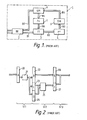
- FIG. 1 there is shown a system block diagram of a heretofore proposed pipeline processing apparatus relying upon data flow control.
- the construction and operation of this processing apparatus are described in detail in the above-referred U.S. Patent Application Serial No. 436,130, and so, only the outline of the construction and operation of the processing apparatus will be described here.
- the processing apparatus includes 6 pipeline stages which are all integrated on an LSI semiconductor chip represented by a dotted-line frame 1.
- the pipeline stages shown in this figure are 6 stages consisting of a bus interface unit (BI) 2, a transfer table memory (TT) 3, a parameter table memory (PT) 4, a data memory (DM) 5, a queue memory (QM) 6 and a processor unit (PU) 7.
- BI bus interface unit
- TT transfer table memory
- PT parameter table memory
- DM data memory
- QM queue memory
- PU processor unit
- any arbitrary one or ones of these stages could be omitted, or another stage could be added further.
- the illustrated respective stages are coupled in a ring form in the sequence of BI-TT-PT-DM-QM-PU by means of buses B l to B 6 according to the pipeline system (hereinafter called pipeline buses), and the circuit is closed on an LSI chip.
- the queue memory (QM) 6 processing is not effected but this stage is used as a cushion for a pipeline.
- An output is transferred from the queue memory (QM) 6 through the bus B 7 to the bus interface unit (BI) 2.
- the bus interface unit (BI) 2 is coupled to input terminals and output terminals of the processing unit so that data transfer can be achieved with the external apparatus.
- the ⁇ bus interface unit (BI) 2 could be coupled to terminals which are common to input and output.
- Data input via the bus interface unit (BI) 2 are transmitted to the transfer table memory (TT) 3 and the pattern table memory (PT) 4.
- TT 3 and PT 4 are stored ID codes indicating destinations of data and OP codes indicating instructions, and they are accessed as addressed by a partial bit or bits of the input data.
- ID code and OP code are jointed in one set and called "template", and an assembly of templates forms a prograi
- generation of an address of the data memory (DM) 5 and read-write control thereof are effected, and also an instruction for the processor unit (PD) 7 is produced.
- the data memory (DM) 5 stores constants to be used for constant calculation and a table for table look-up processing. In addition, this memory is used as a queue for dual data operation or as a buffer for input/output data.
- the queue memory (QM) 6 is used for queuing of data to be transmitted to the PU 7 or the BI 2.
- the processor unit (PU) 7 carries out logic operation, arithmetic operation, and control of data accompanying with modification of an ID code.
- the pipeline processing apparatus in Fig. 1 consists pf 6 units (BI, TT, PT, DM, QM and PU) having the above-described functions, and between one unit and an adjacent unit is provided a latch (hereinafter' called "pipeline latch").
- Fig. 2 is a circuit block diagram prepared by picking up a part of Fig. 1 and enlarging that part.
- a first pipeline stage ST 1 includes one pipeline latch portion (A) 20 and an execution unit 21.
- a second pipeline stage ST 2 includes three pipeline latch portions (B) 22, (C) 23 and (D) 24 and an execution unit 25.
- Pipeline latch portions (E) 26 and (F) 27 located in the subsequent stage are the pipeline latch included in the third pipeline stage ST 3 . More particularly, the data output from ⁇ the pipeline latch portion (A) 20 in the first stage ST 1 to the pipeline bus have the number of data increased by being processed in the execution unit 21.
- the characteristic feature of a data flow control system is that control is effected in such manner that data may flow to the next pipeline stage as accompanied by the data produced newly by processing.
- the second pipeline stage ST 2 are provided three latch portions (B) 22, (C) 23 and (D) 24 which can hold three kinds of data.
- the data in the latch portions (C) 23 and (D) 24 are processed by the execution unit 25 and the result is transmitted to the latch portion (F) 27 in the third pipeline stage ST 3 .
- the data in the latch portion (B) 22 is passed through the pupeline bus without being processed and transmitted to the latch portion (E) 26 in the next pipeline stage ST 3 .
- Fig. 3 is a block diagram of one preferred embodiment of the present invention as applied to a pipeline processing apparatus of data flow control type.
- 6 units (BT 32, TT 33, PT 34, DM 35, QM 36 and PU 37)integrated on a LSI chip 31 have the same functions as those of the corresponding units shown in Fig. 1.
- the respective units are serially connected through pipeline buses B 31 - B 37 -
- data input through input terminals IN are processed through the path of BI-TT-PT-DM-QM-PU-TT-PT-DM-QM-BI, and the result is taken out through output terminals OUT.
- a common bus 38 is formed on the L SI chip 31.
- the opposite ends of the common bus 38 are coupled to a bus B 38 which is coupled to the input terminals IN and to a bus B 39 which is coupled to the output terminals OUT.
- the common bus 38 has contact portions with the respective units so that it may be individually coupled to these units. This common bus 38 is very effectively used upon testing.
- the respective units are provided with pipeline latches as same as Fig. 1.
- the length of the pipeline latches are respectively different depending upon processing carried out in the respective units, all the pipeline latches could have the same length.
- the input terminals IN and the output terminals OUT could be provided as common terminal:
- Fig. 4 is a circuit block diagram showing a part of the circuit in Fig. 3 in an enlarged scale.
- a first pipeline stage-ST 41 having an execution unit 41
- a second pipeline stage ST 42 having an execution unit 45
- pipeline latches 46 and 47 of a third pipeline stage ST 43 which is located in the subsequent stage.
- the first pipeline stage ST 41 has a short pipeline latch 40
- the second pipeline stage ST 42 has a long pipeline latch (42, 43 and 44).
- the respective stages process the data input through the input terminals IN, transfer the processed data to the subsequent stages through a pipeline bus, and the final result of processing is taken out from the output terminals OUT.
- a common bus 48 is formed separately from the pipeline bus, and this common bus 48 is capable of being coupled to the respective pipeline stages.
- the common bus 48 is designed to be capable of being coupled to the respective pipeline latch portions 40, 42, 43, 44, 46 and 47.
- each stage- has a circuit responsive to an address fed from the input terminal IN through the common bus 48 for selecting a designated pipeline latch portion or portions and coupling them to the common bus.
- a common bus 48 independently of the pipeline bus, and provision is made such that by feeding an address through this common bis 48, any arbitrary pipeline stage can be selected to couple the data input and data output of that pipeline stage to the common bus 49.
- the processing unit is constructed in such manner that only a desired pipeline stage can be coupled to the common bus 48 and thereby data can be directly set in the designated stage or data can be directly read out therefrom through the common bus 48. Consequently, only a desired pipeline stage can be selectively tested, and hence an effective test as will be described later can be achieved.
- Fig. 5 is a circuit block diagram which picks up and illustrates in detail a pipeline stage including an execution unit having an ALU 51 and another pipeline stage including an execution unit having memories 55 and 56.
- a pipeline latch portion 50 having a 16-bit length.
- pipeline latch portions 52, 53 and 54 having a 16-bit length, a 14-bit length and a 14-bit length, respectively.
- the pipeline latch portion 52 having a 16-bit length is coupled to an input of a pipeline latch portion 57 (a 16-bit length) in the subsequent stage through a pipeline bus 50.
- the output data from the memories 55 and 56 are alternately switched by a multiplexer (not shown) and are input to a pipeline latch portion 58 (a 16-bit length) in the subsequent stage.
- the data processed by the ALU 51 are expanded as accompanied by newly generated data and/or instruction commands, and are input to the corresponding pipeline latch portions 52, 53 and 54.
- a common bus 59 is wired so as to be capable of being coupled to the respective pipeline latch portions 50, 52, 53, 54, 57 and 58.
- the respective latches have addresses for read and addresses for write, and a read mode and a write mode of the respective latches are controlled by address decoders A50, A52, A53, A54, A57 and A58 associated with the respective latch portions. More particularly, for instance, if an address for reading the data in the latch portion 50 is transferred through the common bus 59, the address decoder A50 would decode this address and would couple the output buffer of the latch portion 50 to the common bus 59. Or else, an address for writing data in the latch portion 52 is transferred through the common bus 59, then the address decoder A52 would decode this address and would couple the input buffer of the latch portion 52 to the common bus 59, so that data on the common bus can be directly set in the latch portion 52.
- common bus 59 could be provided with an address bus and a data bus separately, provision could be made such that an address bus and a data bus are provided in common on a time-division basis by making use of a bus-separator system or a multiplexer system.
- a desired pipeline latch is selected by feeding an address from the input terminals IN to the common bus 59, to directly set data in the selected latch or to directly read out data from the selected latch. Accordingly, for instance, if the latch portion 50 is designated to be in a write mode while the latch portions 52, 53 and 54 are designated to be in a read mode, then only the ALU51 can be selectively checked. If the latch portion 58 is additionally designated, then it is possible to test the memory 55. This is because owing to the provision of the common bus 59 it has become possible to directly set data at a desired latch and to directly take out data from a desired latch by making use of the common bus 59.
- the undesignated latches are discoupled from the common bus 59, they are not adversely effected.
- the clock of to be applied to pipeline stages which are not designated is masked in response to the address.
- test data cannot be set in one operation.
- data can be set in the latch portions 52, 53 and 54 on a time-division basis while the operation of the latch 50 is held stopped by masking of clock, and hence the test between the latches becomes possible. In other words, there is an advantage that a test cycle can be easily controlled externally.
- Fig. 6 is a circuit block diagram of another preferred embodiment of the present invention, in which data in a desired pipeline latch are stacked at an arbitrary timing by making use of the common bus and the stacked data can be taken out externally at a desired time.
- the first stage includes a latch 600 and an input data interface unit 601, and the next stage includes a latch 602, a memory 603 and multiplexe 604 and 605.
- the third stage includes a latch 606, memories 607, 608 and 609 and ALU's 610 and 611, and the fourth stag includes a latch 612 and a data memory 613.
- the fifth stag includes a latch 614 and a queue memory ' 615, and the output of the queue memory 615 is transferred to a latch 619 of an output stage and a latch 616 of a processor unit.
- the processor unit includes the latch 616 and ALU's 617 and 618 and is coupled to the latch 602 in the second stage, and thu pipeline buses are wired in a ring form.
- a common bus 620 which is coupled in common to the latches in the respective stages.
- the latch 602 in the second stage and the latch 614 in the fifth stage are respectively formed in a two-stage latch, and they are respectively associated with auxiliary latches 626 and 627 having the same length.
- auxiliary latches 626 and 627 are both capable of being coupled to the common bus 620, and they have a function of a stack register.
- a stack operation is executed in the following manner. Data indicating commencement of stack are set from the common bus 620 in a register 621, these data are compared in a comparator 622 with data transferred from the unit 601 or the ALU's 617 and 618, and when the both data coincide with each other, the coincidence is detected by a detector 623. Then the detector 623 issues a coincidence signal 624, and in response to this coincidence signal, the auxiliary registers 626 and 627 stack the data then latched in the latches 602 and 614. The stacked data are read out through the common bus 620 when the address designating the respective latches 626 and 627 have been transferred to these latches through the common bus 620.
- Fig. 7 is a block diagram showing a circuit which is effective for checking data that pass through between latches.
- a first pipeline latch includes two latch portions 70 and 71
- a second pipeline latch includes three latch portions 73, 74 and 75.
- the respective latches are associated with address decoders A70, A71, A73, A74 and A75.
- Data set in the latch portion 71 are processed by an ALU 72 and transferred to the latch portions 74 and 75 in the next stage.
- a common bus 76 are coupled to the respective latches and the address decoders.
- modification can be made such that by providing a ROM or PLA 77 in which a fixed code is stored in the preceding stage of the latch 70, the data designating a read mode of the latch 70 are decoded by a decoder 78 and thereby the ROM or PLA 77 may be accessed.
- a predetermined code is set in the latch 70 and this code can be transferred to the latch 73 via the pipeline bus B 71 .
- a transfer test between these latches can be achieved at high speed.
Abstract
Description
- The present invention relates to a processing apparatus having a pipeline structure, and more particularly to a processing apparatus having a function of effecting a logic test and/or a software test within the apparatus.
- A processing apparatus having a pipeline structure is formed by serially coupling a plurality of pipeline stages. Each stage includes a data latch means (hereinafter called pipeline latch) and a processing means, and data to be processed is sequentially shifted via the respective pipeline latches at predetermined pipeline cycle. Especially in a pipeline processing apparatus of a data flow execution model, data tokens input through terminals are accompanied by a processing command which is read out of an internal memory, and they are transferred through the pipeline latches. After the data tokens are processed in each pipeline stages, the result is taken out of output terminals. The detailed structure of this model is discribed in U.S. Patent Application Serial No. 436,130 filed on October 22, 1982 and entitled "Data Processing Machine Suitable For High Speed Processing". This apparatus has many advantages. First of all, the high speed processing can be expected because the respective pipeline stages can operate in parallel computation. Secondly, a multiprocessor system can be easily constructed by coupling the input terminals of one apparatus to the output terminals of another apparatus. Further, many kinds of programs can be processed by means of the same hardware architecture. Moreover, since the large-scaled integrated circuit technique can be employed, at least one pipeline processing apparatus can be integrated on a single semiconductor chip.
- However, only the processing result appears at the output terminals, and none of the intermediate data of the processing appear at the output terminals. More particularly, the input data set is processed by sequential circuits and/or combinational circuits in the pipeline stages and is set in an output latch'as the final result. The output terminals are only coupled to this output latch. Therefore, it is very difficult to know the processing state within the pipeline latches or the logic operations in the respective pipeline stages from the output result. This means that the pipeline processing apparatus of the prior art is not satisfactory in testability. Especially, when the output data to be expected could not be obtained upon testing, it cannot be determined whether the cause of failure exists in a software or in a hardware. If a bug is present in the software, a long period of time is required for discoverir the bug because of poor traceability of a program or poor reservability of intermediate data. On the other hand, in the case where a defect exists in a hardware, it takes also a long period of time for analyzing which circuit is faulty. That is, there is a shortcoming that rectification of design is delayed.
- 'In a pipeline processing apparatus, there are many data sets whose contents are sequentially varied in the respective pipeline stages. In addition, a loop processing is executed only within the apparatus, and its intermediate data does not appear at the output terminals. Furthermore, data which is generated in the midway of the processing and subsequently disappear in the pipeline stages is not derived from the output terminals. Accordingly, so long as the states of the pipeline stages cannot be directly observed externally, it is difficult to improve the testability for the pipe line apparatus.
- Moreover, in a conventional pipeline processing apparatus, processing is advanced at a pipeline cycle that is fixed by the hardware architecture, and a test is also executed at the pipeline cycle. Therefore, a more complex test requiring a long pipeline cycle is impossible. For example, an input of a long test pattern data is not acceptable, because a long period of time is required to apply the test pattern data to the pipeline stages. That is, the prior art pipeline processor has a shortcoming in the point that the pipeline cycle can not be controlled by an external control signal.
- It may be assumed to effect testing by externally leading out signal lines respectively from each pipeline stages. However, in the case where the processing apparatus is formed on an LSI chip, the number of external terminals is limited by the chip size. Further, the package is enlarged in size by the increase of test terminals for the respective stages. In addition, the number of bits of the output data is reduced, and hence the effectiveness of the pipeline processing apparatus which has the merit of high speed processing, would be lost.
- As described above, although the prior art pipeline processing apparatus was favorable for high speed-processing and multi-processing, it was not satisfactory in connection to testabilities such as failure analysis of a hardware, a traceability of an internal state, and a reservability and observabilty intermediate processing data.
- It is therefore one object of the present invention to provide a pipeline processing apparatus having an improved test function.
- Another object of the present invention is to provide a data flow control type processing apparatus having a pipeline structure, including a circuit which can designate any arbitrary pipeline stage so as to directly output the contents of the pipeline latch in that pipeline stage.
- Still another object of the present invention is to provide a pipeline processing apparatus including a circuit which can directly set data in any arbitrary pipeline latch.
- Yet another object of the present invention is to provide a pipeline processor having means for externally controlling a pipeline cycle to permit input of a long data or to enable output of the contents of the pipeline latch at any arbitrary timing.
- A still further object of the present invention is to provide a pipeline processor which can simply test passing through of data between the pipeline latches.
- A further more object of the present invention is to provide a pipeline processing apparatus in which a circuit for testing the respective pipeline stages is formed on an LSI chip without increasing the number of input and output terminals.
- Still another object of the present invention is to provide a pipeline processing apparatus having a circuit for setting a test data to be required in a designated pipeline latch without inputting test data.
- Yet another object of the present invention is to provide a pipeline processing machine having functions to temporarily stack at least one intermediate processing data and to observe the stacked data at desired timing.
- A pipeline processing apparatus of the present invention comprises a plurality of pipeline stages, a pipeline bus for serially coupling the pipeline stages, an input portion for applying data to be processed to a first pipeline stage, an output portion for taking out data which has been processed in the pipeline stages, a common bus coupled to the input portion and the output portion and having a plurality of coupling portions to which the pipeline stages are coupled, a first circuitry for designing at least one pipeline stage, a second circuitry for coupling the designated pipeline stage to the associated coupling portion of the common bus, and a third circuitry for setting data on the common bus in the designated pipeline stage and/or for reading out data of the designated pipeline stage to the common bus.
- According to the present invention, since the common bus used as an input and/or an output of the test data is provided in the pipeline apparatus, any arbitrary pipeline stage can be tested without using the pipeline bus. ` Particularly, the test data is directly set in a selected pipeline stage through the common bus, and/or the data in the selected pipeline stage is directly read out. Accordingly, observation of the states of the pipeline stages has become possible, and hence testability of the pipeline processing apparatus can be greatly improved. Furthermore an intermediate data of the processing can be selectively checked, and thereby a partial test can be executed. This is very effective not only for makers but also for users. Furthermore, since the coupling between the pipeline stages and the common bus can be externally controlled by making use of the first circuitry (the designation circuit) for pipeline stages, data can be transferred to a desired pipeline stage while by-passing unnecessary pipeline stage, and thereby only a partial stage can be tested at a high speed.
- Furthermore, the selected pipeline stages are coupled to the common bus and the remaining pipeline stages are discoupled from the common bus, and therefore, a pipeline cycle can be freely controlled externally. It is also easy to stop the operation of the pipeline stages-discoupled from the common bus. This is an advantage for a pipeline processing apparatus which is designed so as to operate . at a fixed speed according to a basic clock. The respective pipeline stages can operate as a temporarily latch circuitry by stopping their operation. In this operation, the basic clock may be masked so as not to apply to the pipeline stages. Under such condition, the data setting and/or the data reading- out is carried out at a desired timing. Accordingly, the input/output of test data can be executed independently of the basic clock. This is especially effective in a data flow control system. In a data flow control system, various commands and new data are generated in each pipeline stage, and these generated commands and new data are transferred through a pipeline bus to the pipeline latch of the next pipeline stage with data to be processed. Accordingly, the number of bits of pipeline latches of the pipeline stages are normally larger than the number of the input terminals of the processing apparatus. Consequently, the test data transferred via the common bus from the input terminals to the long pipeline latch must be transmitted on a time-division basis. However, in the case where a pipeline stage includes a sequential circuit or the like, the state of the pipeline stage may change during the time-division data transfer. On the other hand, the present invention can stop the internal basic clock and can control the operation timing externally. Therefore, test data that is longer than the number of input terminals can be directly set in the pipeline latch without changing of the state in the pipeline stage.
- Furthermore, to control the pipeline cycle externally as described above is very effective not only for input of data into the pipeline latch but also for externally output of data in the pipeline latch through the common bus. For instance, a taking-out of data, which are longer than the number of the output terminals from the pipeline latch, must be derived on a time-division basis. In such a case, since the taking-out can,be done while stopping the operation of the other stages, and can be done without destroying the pipeline processing flow.
- Furthermore, the respective pipeline latches may be formed in a two-stage latch construction, in which the first pipeline latch in the two-stage latch structure is coupled to the pipeline bus and the common bus and the second pipeline latch is coupled to the first pipeline latch and the common bus. In this construction, by designating a pipeline stage, the contents in the first latch of the designated pipeline stage are stacked in the second latch. That is, the second latch is used as a stack register. As a result, the state of the stage under any arbitrary timing can be preserved without interrupting a processing flow in the respective-pipeline stages. And by taking out the contents in the second latch through the common bus, the state of the stage can be observed at any desired time point. Furthermore, the contents can be transmitted to another pipeline stage at any arbitrary timing. In this way, since dump of the data within°the latch can be done, a virtual pipeline cycle can be made variable without disturbing processing flow of the pipeline data. Consequently, in parallel to test processing, the contents in the respective latches can be checked independently of each other. Moreover, this function'is effective not only for testing but also for dump processing upon normal pipeline processing.
- Furthermore, as the pipeline stage designating circuit, the conventional address decode system can be employed.
- An address decoder is provided in each pipeline stage and designating addresses of pipeline stages are fed through the common bus. As a result, only the desired pipeline stages are selected, and the other pipeline stages are electrically disconnected from the common bus. Under this condition, selective testing between the desired pipeline stages becomes possible. Among the data flowing through the pipeline bus, there are such data that are not subjected to processing in a certain stage but in themselves passed therethrough to the next stage. A pipeline processing apparatus is however, characterized in that the respective pipeline stages necessarily have pipeline latches so that the processings of the respective pipeline stages may be synchronized. In other words, the number of pipeline latches are as same as the number of the pipeline cycles, and every data may be shifted through all the provided pipeline latches. Accordingly, among the data to be processed, there is the data which is merely passed through without being subjected to processing. With respect to such data, it is more desirable that transfer check can be done only between the latches before and behind the pipeline stage through which the data- are passed through. The present invention is favorable for a test between one latch and the subsequent latch. These latches are addressed via the common bus and are coupled to the common bus. In this way, the preceding latch is set on the siting condition, while the succeeding latch is set on the reading condition. The test data is set into the preceding latch through the common bus. The set data are transferred to the latch in the succeeding stage via the pipeline bus. The transferred data are read out from the latch in the succeeding stage to the common bus and are in themselves taken out externally. Accordingly, when the taken out data are checked, if they are identical to the input data, then the passing through between the respective latches is good, whereas if the respective data are different, it can be easily found within a short period of time that there exists a fault in the passing through between these latches. On the other hand, in some cases there are not provided a sufficient number of input terminals for enabling to transfer check data jointly with an address for designating a pipeline stage through which data are passed, and in other cases, a check data set is so long that it cannot be set in a latch in one operation. In there cases, a memory or a PLA (programmable logic array), in which a data set for checking is stored, may be employed, and in response to an address designating a pipeline stage through which data are passed, or in response to a pseudo-address formed by subjecting the aforementioned address to control or modification, the employed memory or PLA is accessed and check data is read therefrom and is set in the designated pipeline latch. By making such provision, data through check can be done at a further high speed.
- As described above, according to the present invention, test processing which was impossible in the pipeline processing apparatus in the prior art, can be achieved easily by making use of a common bus without disturbing a flow of pipeline processing. Especially, either a test conducted through all the pipeline stages or a test conducted through only a desired stage or stages can be executed by switching selectively. In-addition, dump processing in which contents in a desired pipeline latch are stacked is also possible, and this is available not only for test processing but also for normal pipeline processing.
- The above-mentioned and other objects, features and advantages of the present invention will become more apparent by reference to the following description of preferred embodiments of the invention taken in conjunction with the accompanying drawings.
-
- Fig. 1 is a block diagram of a data flow type pipeline processing apparatus in the prior art;
- Fig. 2 is an enlarged block diagram of a part of the circuit shown in Fig. 1, three stages of pipeline latches being included in this figure;
- Fig. 3 is a block diagram of a data flow type pipeline processing apparatus according to one preferred embodiment of the present invention;
- Fig. 4 is a circuit block diagram showing a part of the pipeline processing apparatus shown in Fig. 3, three stages of pipeline latches being included in this figure;
- Fig. 5 is an enlarged circuit block diagram of an essential part of the pipeline processing apparatus in Fig. 3;
- Fig. 6 is a circuit block diagram showing another preferred embodiment of the pipeline processing apparatus according to the present invention; and
- Fig. 7 is a partial enlarged circuit block diagram of a pipeline stage used in one part of a pipeline processing apparatus according to still another preferred embodiment of the present invention.
- Referring now to Fig. 1, there is shown a system block diagram of a heretofore proposed pipeline processing apparatus relying upon data flow control. The construction and operation of this processing apparatus are described in detail in the above-referred U.S. Patent Application Serial No. 436,130, and so, only the outline of the construction and operation of the processing apparatus will be described here. The processing apparatus includes 6 pipeline stages which are all integrated on an LSI semiconductor chip represented by a dotted-
line frame 1. The pipeline stages shown in this figure are 6 stages consisting of a bus interface unit (BI) 2, a transfer table memory (TT) 3, a parameter table memory (PT) 4, a data memory (DM) 5, a queue memory (QM) 6 and a processor unit (PU) 7. As a matter of course, in another pipeline processing apparatus, any arbitrary one or ones of these stages could be omitted, or another stage could be added further. The illustrated respective stages are coupled in a ring form in the sequence of BI-TT-PT-DM-QM-PU by means of buses Bl to B6 according to the pipeline system (hereinafter called pipeline buses), and the circuit is closed on an LSI chip. In the queue memory (QM) 6, processing is not effected but this stage is used as a cushion for a pipeline. An output is transferred from the queue memory (QM) 6 through the bus B7 to the bus interface unit (BI) 2. The bus interface unit (BI) 2 is coupled to input terminals and output terminals of the processing unit so that data transfer can be achieved with the external apparatus. It is to be noted that the`bus interface unit (BI) 2 could be coupled to terminals which are common to input and output. Data input via the bus interface unit (BI) 2 are transmitted to the transfer table memory (TT) 3 and the pattern table memory (PT) 4. In the TT 3 and PT 4 are stored ID codes indicating destinations of data and OP codes indicating instructions, and they are accessed as addressed by a partial bit or bits of the input data. These ID code and OP code are jointed in one set and called "template", and an assembly of templates forms a prograi By the data read from the PT 4, generation of an address of the data memory (DM) 5 and read-write control thereof are effected, and also an instruction for the processor unit (PD) 7 is produced. The data memory (DM) 5 stores constants to be used for constant calculation and a table for table look-up processing. In addition, this memory is used as a queue for dual data operation or as a buffer for input/output data. The queue memory (QM) 6 is used for queuing of data to be transmitted to the PU 7 or theBI 2. The processor unit (PU) 7 carries out logic operation, arithmetic operation, and control of data accompanying with modification of an ID code. The pipeline processing apparatus in Fig. 1 consistspf 6 units (BI, TT, PT, DM, QM and PU) having the above-described functions, and between one unit and an adjacent unit is provided a latch (hereinafter' called "pipeline latch"). As a result, input, output and processing of data can be achieved in parallel within the respective stapes, and hence a high performance can be obtained. It is to be noted that in each block if it is necessary depending upon a processing time and processing contents, the block could be divided into a plurality of blocks. - In such a processing unit, data are passed through the respective data buses and processed in the respective stages. They are transferred sequentially through the ring as accompanies by newly produced data and instruction commands. The final result is output from the
QM 6 to the bus B7 and the result appears at external output terminals via the BI 2. Accordingly, the lengths of the pipeline latches associated with the respective units are different, and especially it is a common practice that the latches of the units other than the latch in theBI 2 which is coupled to the external terminals are longer than the latch in theBI 2. This state is shown in Fig. 2. Fig. 2 is a circuit block diagram prepared by picking up a part of Fig. 1 and enlarging that part. this diagram includes three pipeline latches and two units between these latches. A first pipeline stage ST1 includes one pipeline latch portion (A) 20 and anexecution unit 21. A second pipeline stage ST2 includes three pipeline latch portions (B) 22, (C) 23 and (D) 24 and anexecution unit 25. Pipeline latch portions (E) 26 and (F) 27 located in the subsequent stage are the pipeline latch included in the third pipeline stage ST3. More particularly, the data output from`the pipeline latch portion (A) 20 in the first stage ST1 to the pipeline bus have the number of data increased by being processed in theexecution unit 21. The characteristic feature of a data flow control system is that control is effected in such manner that data may flow to the next pipeline stage as accompanied by the data produced newly by processing. Accordingly, in the second pipeline stage ST2 are provided three latch portions (B) 22, (C) 23 and (D) 24 which can hold three kinds of data. Among these data, the data in the latch portions (C) 23 and (D) 24 are processed by theexecution unit 25 and the result is transmitted to the latch portion (F) 27 in the third pipeline stage ST3. On the other hand, the data in the latch portion (B) 22 is passed through the pupeline bus without being processed and transmitted to the latch portion (E) 26 in the next pipeline stage ST3. - In the pipeline processing apparatus having the above-mentioned circuit construction in the prior art, as will be apparent from Fig. 1, data fed externally are allowed to be input only through the external input terminals coupled to the bus interface unit (BI) 2. Moreover, the input data are allowed to be transferred only through the pipeline buses. In addition, the sequence of transfer is also fixed, and basically the transfer path cannot be modified to a sequence other than the sequence of BI-TT-DT-DM-QM-PU-TT-PT-DM-QM-BI. In other words, data cannot be transferred to the next stage unless they pass through a pipeline stage coupled immediately therebehind. However, when data is moved through a pipeline stage,the data is processed.in that stage, in some case the contents of the data would be varied. Accordingly, for testing such a processing apparatus in the prior art, there was no way except for the method of checking the final result (the output data appearing at the output terminals) after the input'test data have been processed. In other words, test of whether the hardware or software of the processing apparatus is good or bad only, could be done. However, under such situation, it is very difficult to detect what portion is faulty. Especially in the design of hardwares and in the development of softwares, analysis of the cause of faults is most important.
- What is considered to be a cause which brings about faults of a processing unit is that the individual logic elements are not achieving proper operation, a programmed instruction is not correctly executed, or that a program itself includes errors. However, it was difficult in the pipeline processing apparatus in the prior art to make analysis within a short period of time on what logic element is abnormal, which is the pipeline stage in which an instruction is not correctly executed, and what instruction in the program is faulty. For stance, even if a fault exists in the
execution unit 21 in Fig. 2, since the contents of the latch portions (B) 22, (C) 23 and (D) 24 cannot be checked directly, the analysis of the faulty location (unit.21) is difficult. Furthermore, since independent test for each stage unit cannot be effected, even if it is assumed that a fault exists only in the second pipeline stage ST2, the location of the fault in the pipeline stage ST2-cannot be searched. Especially, since the pipeline latch portions (B), (C) and (D) in the second stage are longer than the pipeline latch portion (A) in the preceding stage, test data cannot be set in the pipeline latch portsions (B), (C) and (D) without being subjected processing in theexecution unit 21. Furthermore, since it is impossible to pick up and check a portion through which data are passed without being processed such as the pipeline bus between the latch portion (B) 22 and the latch portion (E) 26. That is, checking of a pipeline bus is also impossible. In addition, in each pipeline stage since processing is effected on the basis of a predetermined pipeline cycle, it is further impossible to preserve the contents of the latch at any arbitrary timing. - Fig. 3 is a block diagram of one preferred embodiment of the present invention as applied to a pipeline processing apparatus of data flow control type. 6 units (
BT 32,TT 33,PT 34,DM 35,QM 36 and PU 37)integrated on aLSI chip 31 have the same functions as those of the corresponding units shown in Fig. 1. In addition, similarly to Fig. 1, the respective units are serially connected through pipeline buses B31 - B37- In normal pipeline processing, data input through input terminals IN are processed through the path of BI-TT-PT-DM-QM-PU-TT-PT-DM-QM-BI, and the result is taken out through output terminals OUT. In addition, if required, loop processing is effected within the ring consisting of TT-PT-DM-QM-PU-TT. What is different from the circuit shown in Fig. 1 is that acommon bus 38 is formed on the LSI chip 31. The opposite ends of thecommon bus 38 are coupled to a bus B38 which is coupled to the input terminals IN and to a bus B39 which is coupled to the output terminals OUT. Furthermore, thecommon bus 38 has contact portions with the respective units so that it may be individually coupled to these units. Thiscommon bus 38 is very effectively used upon testing. The respective units are provided with pipeline latches as same as Fig. 1. Moreover, though the length of the pipeline latches are respectively different depending upon processing carried out in the respective units, all the pipeline latches could have the same length. Furthermore, the input terminals IN and the output terminals OUT could be provided as common terminal: - Fig. 4 is a circuit block diagram showing a part of the circuit in Fig. 3 in an enlarged scale. In this figure are included a first pipeline stage-ST41 having an
execution unit 41, a second pipeline stage ST42 having anexecution unit 45, and pipeline latches 46 and 47 of a third pipeline stage ST43 which is located in the subsequent stage. The first pipeline stage ST41 has ashort pipeline latch 40, while the second pipeline stage ST42 has a long pipeline latch (42, 43 and 44). The respective stages process the data input through the input terminals IN, transfer the processed data to the subsequent stages through a pipeline bus, and the final result of processing is taken out from the output terminals OUT. In addition, acommon bus 48 is formed separately from the pipeline bus, and thiscommon bus 48 is capable of being coupled to the respective pipeline stages. In Fig. 4, thecommon bus 48 is designed to be capable of being coupled to the respectivepipeline latch portions common bus 48 for selecting a designated pipeline latch portion or portions and coupling them to the common bus. - According to the above-described embodiment of the pipeline processing apparatus, there is provided a
common bus 48 independently of the pipeline bus, and provision is made such that by feeding an address through thiscommon bis 48, any arbitrary pipeline stage can be selected to couple the data input and data output of that pipeline stage to the common bus 49. In other words, the processing unit is constructed in such manner that only a desired pipeline stage can be coupled to thecommon bus 48 and thereby data can be directly set in the designated stage or data can be directly read out therefrom through thecommon bus 48. Consequently, only a desired pipeline stage can be selectively tested, and hence an effective test as will be described later can be achieved. In addition, since an operation timing-of a pipeline stage can be externally controlled independently at a separate cycle from the predetermined pipeline cycle, it is possible to set data at a desired stage on a time-division basis, to derive data from the stage on a time-division basis, or to take out data in an arbitrary timing at a desired time. These effective advantages obtained according to the present invention will be explained in the following with reference to Figs. 5 to 7. - Fig. 5 is a circuit block diagram which picks up and illustrates in detail a pipeline stage including an execution unit having an
ALU 51 and another pipeline stage including an executionunit having memories ALU 51 is provided apipeline latch portion 50 having a 16-bit length. On the other hand, in the stage having thememories pipeline latch portions pipeline latch portion 52 having a 16-bit length is coupled to an input of a pipeline latch portion 57 (a 16-bit length) in the subsequent stage through apipeline bus 50. On the other hand, the output data from thememories ALU 51 are expanded as accompanied by newly generated data and/or instruction commands, and are input to the correspondingpipeline latch portions common bus 59 is wired so as to be capable of being coupled to the respectivepipeline latch portions latch portion 50 is transferred through thecommon bus 59, the address decoder A50 would decode this address and would couple the output buffer of thelatch portion 50 to thecommon bus 59. Or else, an address for writing data in thelatch portion 52 is transferred through thecommon bus 59, then the address decoder A52 would decode this address and would couple the input buffer of thelatch portion 52 to thecommon bus 59, so that data on the common bus can be directly set in thelatch portion 52. Here it is to be noted that although thecommon bus 59 could be provided with an address bus and a data bus separately, provision could be made such that an address bus and a data bus are provided in common on a time-division basis by making use of a bus-separator system or a multiplexer system. - By constructing a pipeline processing apparatus in the above-described manner, it is possible that a desired pipeline latch is selected by feeding an address from the input terminals IN to the
common bus 59, to directly set data in the selected latch or to directly read out data from the selected latch. Accordingly, for instance, if thelatch portion 50 is designated to be in a write mode while thelatch portions latch portion 58 is additionally designated, then it is possible to test thememory 55. This is because owing to the provision of thecommon bus 59 it has become possible to directly set data at a desired latch and to directly take out data from a desired latch by making use of thecommon bus 59. On the other hand, since the undesignated latches are discoupled from thecommon bus 59, they are not adversely effected. The clock of to be applied to pipeline stages which are not designated is masked in response to the address. When a test is conducted between thelatch portions latch portions latch portions latch portions ALU 51 in the preceding stage, if anomaly exists in theALU 51, this test cannot be achieved. Even if anomaly does not exist in theALU 51, in the case where the ALU includes a sequential circuit, the data would be changed. Furthermore, even if the processing in theALU 51 is stopped, since the latch consisting of 52, 53 and 54 are longer than thelatch 50, test data cannot be set in one operation. However, by providing thecommon bus 59 according to this preferred, embodiment, data can be set in thelatch portions latch 50 is held stopped by masking of clock, and hence the test between the latches becomes possible. In other words, there is an advantage that a test cycle can be easily controlled externally. - Fig. 6 is a circuit block diagram of another preferred embodiment of the present invention, in which data in a desired pipeline latch are stacked at an arbitrary timing by making use of the common bus and the stacked data can be taken out externally at a desired time. In this figure are included 6 pipeline stages. The first stage includes a
latch 600 and an inputdata interface unit 601, and the next stage includes alatch 602, amemory 603 and multiplexe 604 and 605. The third stage includes alatch 606,memories latch 612 and adata memory 613. The fifth stag includes alatch 614 and aqueue memory ' 615, and the output of thequeue memory 615 is transferred to alatch 619 of an output stage and alatch 616 of a processor unit. The processor unit includes thelatch 616 and ALU's 617 and 618 and is coupled to thelatch 602 in the second stage, and thu pipeline buses are wired in a ring form. In addition, there is provided acommon bus 620 which is coupled in common to the latches in the respective stages. Thelatch 602 in the second stage and thelatch 614 in the fifth stage are respectively formed in a two-stage latch, and they are respectively associated withauxiliary latches common bus 620, and they have a function of a stack register. A stack operation is executed in the following manner. Data indicating commencement of stack are set from thecommon bus 620 in a register 621, these data are compared in acomparator 622 with data transferred from theunit 601 or the ALU's 617 and 618, and when the both data coincide with each other, the coincidence is detected by adetector 623. Then thedetector 623 issues acoincidence signal 624, and in response to this coincidence signal, theauxiliary registers latches common bus 620 when the address designating therespective latches common bus 620. - As a result, the contents of the latch at any arbitrary timing have been stacked in the corresponding auxiliary latch: without stopping the pipeline processing, and the stacked data can be taken out at a desired time. Accordingly, not only test processing, but also dump operation during normal pipeline processing becomes possible, and hence this arrangement is very effective. It is to be noted that modification could be made such that the stage of the
detector 623 is read out through thecommon bus 620 so as to be able to be observed externally. Alternatively, the data indicating a stack operation could be set in the register 621 from the pipeline bus through anadditional bus 626 represented by a dotted line. - Fig. 7 is a block diagram showing a circuit which is effective for checking data that pass through between latches. In this figure, a first pipeline latch includes two
latch portions latch portions latch portion 71 are processed by an ALU 72 and transferred to thelatch portions common bus 76 are coupled to the respective latches and the address decoders. - Unless the
common bus 76 is provided, checking of the data passing through between thelatch 70 and thelatch 73 is impossible. This is because the data incoming through the pipeline bus B70 have their contents modified by the processing in the preceding stage and so it cannot be checked what data have been set in thelatch 70. However, by providing thecommon bus 76 as shown in Fig. 7, a particular latch can be designated and data can be directly set in the designated latch, so that the aforementioned shortcoming can be overcome. But, in the case of feeding the data to be set in thelatch 70 from thecommon bus 76, a test period will be prolonged by the corresponding amount. Accordingly, as shown in Fig.7, modification can be made such that by providing a ROM orPLA 77 in which a fixed code is stored in the preceding stage of thelatch 70, the data designating a read mode of thelatch 70 are decoded by adecoder 78 and thereby the ROM orPLA 77 may be accessed. As a result, a predetermined code is set in thelatch 70 and this code can be transferred to thelatch 73 via the pipeline bus B71. Thereafter, by taking out the data in thelatch 73 through thecommon bus 76, a transfer test between these latches can be achieved at high speed. - As described above, according to the present invention, a test can be achieved without disturbing a pipeline, and the aforementioned various advantages can be obtained.
Claims (9)
Applications Claiming Priority (2)
| Application Number | Priority Date | Filing Date | Title |
|---|---|---|---|
| JP90620/82 | 1982-05-28 | ||
| JP57090620A JPS58207152A (en) | 1982-05-28 | 1982-05-28 | Test system for pipeline arithmetic device |
Publications (3)
| Publication Number | Publication Date |
|---|---|
| EP0095928A2 true EP0095928A2 (en) | 1983-12-07 |
| EP0095928A3 EP0095928A3 (en) | 1985-01-30 |
| EP0095928B1 EP0095928B1 (en) | 1989-04-12 |
Family
ID=14003527
Family Applications (1)
| Application Number | Title | Priority Date | Filing Date |
|---|---|---|---|
| EP83303113A Expired EP0095928B1 (en) | 1982-05-28 | 1983-05-31 | Pipeline processing apparatus having a test function |
Country Status (4)
| Country | Link |
|---|---|
| US (1) | US4658354A (en) |
| EP (1) | EP0095928B1 (en) |
| JP (1) | JPS58207152A (en) |
| DE (1) | DE3379610D1 (en) |
Cited By (4)
| Publication number | Priority date | Publication date | Assignee | Title |
|---|---|---|---|---|
| EP0228207A2 (en) * | 1985-12-17 | 1987-07-08 | Advanced Micro Devices, Inc. | Built-in test circuitry for combinatorial logic |
| EP0264947A2 (en) * | 1986-10-23 | 1988-04-27 | The Grass Valley Group, Inc. | Diagnostic system for a digital signal processor |
| EP0126785B1 (en) * | 1983-05-25 | 1989-03-08 | Ibm Deutschland Gmbh | Test and diagnostic device for a digital computer |
| US7237858B2 (en) | 2002-03-14 | 2007-07-03 | Seiko Epson Corporation | Printing apparatus, printing method, storage medium, and computer system |
Families Citing this family (28)
| Publication number | Priority date | Publication date | Assignee | Title |
|---|---|---|---|---|
| JPS60239834A (en) * | 1984-05-14 | 1985-11-28 | Nec Corp | Integrated circuit |
| US4858115A (en) * | 1985-07-31 | 1989-08-15 | Unisys Corporation | Loop control mechanism for scientific processor |
| JPS6413627A (en) * | 1987-07-07 | 1989-01-18 | Nec Corp | Pipeline register |
| US4845663A (en) * | 1987-09-03 | 1989-07-04 | Minnesota Mining And Manufacturing Company | Image processor with free flow pipeline bus |
| US5535331A (en) * | 1987-09-04 | 1996-07-09 | Texas Instruments Incorporated | Processor condition sensing circuits, systems and methods |
| JPS6484339A (en) * | 1987-09-28 | 1989-03-29 | Nec Corp | Lsi testing circuit |
| JP2584654B2 (en) * | 1988-03-18 | 1997-02-26 | 富士通株式会社 | Data processing device |
| US5099421A (en) * | 1988-12-30 | 1992-03-24 | International Business Machine Corporation | Variable length pipe operations sequencing |
| JP3147432B2 (en) * | 1991-10-09 | 2001-03-19 | 株式会社日立製作所 | Pipeline processing equipment |
| US5603012A (en) * | 1992-06-30 | 1997-02-11 | Discovision Associates | Start code detector |
| US5461571A (en) * | 1992-11-17 | 1995-10-24 | Honeywell Inc. | Complementary thread display method and apparatus |
| US5995996A (en) * | 1993-06-15 | 1999-11-30 | Xerox Corporation | Pipelined image processing system for a single application environment |
| US5701479A (en) * | 1993-06-15 | 1997-12-23 | Xerox Corporation | Pipelined image processing system for a single application environment |
| US5557795A (en) * | 1993-06-15 | 1996-09-17 | Xerox Corporation | Pipelined image processing system for a single application environment |
| JPH08194679A (en) * | 1995-01-19 | 1996-07-30 | Texas Instr Japan Ltd | Method and device for processing digital signal and memory cell reading method |
| US5699506A (en) * | 1995-05-26 | 1997-12-16 | National Semiconductor Corporation | Method and apparatus for fault testing a pipelined processor |
| US5732209A (en) * | 1995-11-29 | 1998-03-24 | Exponential Technology, Inc. | Self-testing multi-processor die with internal compare points |
| WO1999050852A1 (en) | 1998-04-01 | 1999-10-07 | Mosaid Technologies Incorporated | Semiconductor memory asynchronous pipeline |
| WO2001033351A1 (en) * | 1999-10-29 | 2001-05-10 | Fujitsu Limited | Processor architecture |
| KR100872213B1 (en) | 2000-07-07 | 2008-12-05 | 모사이드 테크놀로지스, 인코포레이티드 | A method for performing a read command in a memory device |
| AU2003285636A1 (en) | 2002-12-30 | 2004-07-22 | Koninklijke Philips Electronics N.V. | Birefringent optical component |
| US8050866B2 (en) * | 2003-09-25 | 2011-11-01 | Halliburton Energy Services, Inc. | Pulsed-neutron formation density |
| US7250953B2 (en) * | 2004-05-14 | 2007-07-31 | Nvidia Corporation | Statistics instrumentation for low power programmable processor |
| US7389006B2 (en) * | 2004-05-14 | 2008-06-17 | Nvidia Corporation | Auto software configurable register address space for low power programmable processor |
| US7091982B2 (en) * | 2004-05-14 | 2006-08-15 | Nvidia Corporation | Low power programmable processor |
| US7895280B2 (en) | 2008-09-03 | 2011-02-22 | Microsoft Corporation | Composing message processing pipelines |
| US20160328237A1 (en) * | 2015-05-07 | 2016-11-10 | Via Alliance Semiconductor Co., Ltd. | System and method to reduce load-store collision penalty in speculative out of order engine |
| KR102508309B1 (en) * | 2018-04-23 | 2023-03-10 | 에스케이하이닉스 주식회사 | Pipe latch, semiconductor apparatus and semiconductor system using the same |
Citations (3)
| Publication number | Priority date | Publication date | Assignee | Title |
|---|---|---|---|---|
| US4023142A (en) * | 1975-04-14 | 1977-05-10 | International Business Machines Corporation | Common diagnostic bus for computer systems to enable testing concurrently with normal system operation |
| US4183461A (en) * | 1977-03-14 | 1980-01-15 | Tokyo Shibaura Electric Co., Ltd. | Fault-diagnosing method for an electronic computer |
| US4253183A (en) * | 1979-05-02 | 1981-02-24 | Ncr Corporation | Method and apparatus for diagnosing faults in a processor having a pipeline architecture |
Family Cites Families (10)
| Publication number | Priority date | Publication date | Assignee | Title |
|---|---|---|---|---|
| US3980992A (en) * | 1974-11-26 | 1976-09-14 | Burroughs Corporation | Multi-microprocessing unit on a single semiconductor chip |
| US4149242A (en) * | 1977-05-06 | 1979-04-10 | Bell Telephone Laboratories, Incorporated | Data interface apparatus for multiple sequential processors |
| US4305124A (en) * | 1978-06-09 | 1981-12-08 | Ncr Corporation | Pipelined computer |
| US4385363A (en) * | 1978-12-15 | 1983-05-24 | Compression Labs, Inc. | Discrete cosine transformer |
| US4395698A (en) * | 1980-08-15 | 1983-07-26 | Environmental Research Institute Of Michigan | Neighborhood transformation logic circuitry for an image analyzer system |
| US4398176A (en) * | 1980-08-15 | 1983-08-09 | Environmental Research Institute Of Michigan | Image analyzer with common data/instruction bus |
| US4443859A (en) * | 1981-07-06 | 1984-04-17 | Texas Instruments Incorporated | Speech analysis circuits using an inverse lattice network |
| US4414669A (en) * | 1981-07-23 | 1983-11-08 | General Electric Company | Self-testing pipeline processors |
| US4441207A (en) * | 1982-01-19 | 1984-04-03 | Environmental Research Institute Of Michigan | Design rule checking using serial neighborhood processors |
| US4484349A (en) * | 1982-03-11 | 1984-11-20 | Environmental Research Institute Of Michigan | Parallel pipeline image processor |
-
1982
- 1982-05-28 JP JP57090620A patent/JPS58207152A/en active Granted
-
1983
- 1983-05-31 US US06/499,705 patent/US4658354A/en not_active Expired - Lifetime
- 1983-05-31 EP EP83303113A patent/EP0095928B1/en not_active Expired
- 1983-05-31 DE DE8383303113T patent/DE3379610D1/en not_active Expired
Patent Citations (3)
| Publication number | Priority date | Publication date | Assignee | Title |
|---|---|---|---|---|
| US4023142A (en) * | 1975-04-14 | 1977-05-10 | International Business Machines Corporation | Common diagnostic bus for computer systems to enable testing concurrently with normal system operation |
| US4183461A (en) * | 1977-03-14 | 1980-01-15 | Tokyo Shibaura Electric Co., Ltd. | Fault-diagnosing method for an electronic computer |
| US4253183A (en) * | 1979-05-02 | 1981-02-24 | Ncr Corporation | Method and apparatus for diagnosing faults in a processor having a pipeline architecture |
Cited By (6)
| Publication number | Priority date | Publication date | Assignee | Title |
|---|---|---|---|---|
| EP0126785B1 (en) * | 1983-05-25 | 1989-03-08 | Ibm Deutschland Gmbh | Test and diagnostic device for a digital computer |
| EP0228207A2 (en) * | 1985-12-17 | 1987-07-08 | Advanced Micro Devices, Inc. | Built-in test circuitry for combinatorial logic |
| EP0228207A3 (en) * | 1985-12-17 | 1989-03-22 | Advanced Micro Devices, Inc. | Built-in test circuitry for combinatorial logic |
| EP0264947A2 (en) * | 1986-10-23 | 1988-04-27 | The Grass Valley Group, Inc. | Diagnostic system for a digital signal processor |
| EP0264947A3 (en) * | 1986-10-23 | 1990-06-20 | The Grass Valley Group, Inc. | Diagnostic system for a digital signal processor |
| US7237858B2 (en) | 2002-03-14 | 2007-07-03 | Seiko Epson Corporation | Printing apparatus, printing method, storage medium, and computer system |
Also Published As
| Publication number | Publication date |
|---|---|
| EP0095928B1 (en) | 1989-04-12 |
| JPS58207152A (en) | 1983-12-02 |
| US4658354A (en) | 1987-04-14 |
| EP0095928A3 (en) | 1985-01-30 |
| JPH0126097B2 (en) | 1989-05-22 |
| DE3379610D1 (en) | 1989-05-18 |
Similar Documents
| Publication | Publication Date | Title |
|---|---|---|
| EP0095928A2 (en) | Pipeline processing apparatus having a test function | |
| EP0111053B1 (en) | On-chip monitor | |
| KR100328357B1 (en) | Improved redundancy analyzer for automatic memory tester | |
| US5557558A (en) | Microprocessor with self-diagnostic test function | |
| JP3176482B2 (en) | Logic simulation equipment | |
| JPWO2008053709A1 (en) | Semiconductor integrated circuit sorting test apparatus and method | |
| US4422141A (en) | Microprocessor architecture for improved chip testability | |
| EP0497485A2 (en) | Computer for implementing two-operand instructions | |
| US4660198A (en) | Data capture logic for VLSI chips | |
| ITRM20010644A1 (en) | MEMORY TESTING EQUIPMENT WITH INCREASED POST-DECODING. | |
| KR100321274B1 (en) | Pipeline-type multi-processor system | |
| US8046643B2 (en) | Transport subsystem for an MBIST chain architecture | |
| US6289473B1 (en) | Semiconductor device having a debug function | |
| US5050076A (en) | Prefetching queue control system | |
| US7058870B2 (en) | Method and apparatus for isolating faulty semiconductor devices in a multiple stream graphics system | |
| US6457150B1 (en) | Method and apparatus for on-chip monitoring of integrated circuits with a distributed system | |
| US7043417B1 (en) | High speed software driven emulator comprised of a plurality of emulation processors with improved multiplexed data memory | |
| US11506710B1 (en) | Method for testing a circuit system and a circuit system thereof | |
| JP2792327B2 (en) | Semiconductor integrated circuit device | |
| JPS5860363A (en) | Operation hysteresis storing system for logical device | |
| JP3089249B2 (en) | Associative memory device | |
| JP2003114259A (en) | Lsi test method and device therefor | |
| JPH0792768B2 (en) | Microcomputer | |
| JP2001350645A (en) | Computer system | |
| JPH0520119A (en) | Scan data supplying device |
Legal Events
| Date | Code | Title | Description |
|---|---|---|---|
| PUAI | Public reference made under article 153(3) epc to a published international application that has entered the european phase |
Free format text: ORIGINAL CODE: 0009012 |
|
| AK | Designated contracting states |
Designated state(s): DE FR GB |
|
| PUAL | Search report despatched |
Free format text: ORIGINAL CODE: 0009013 |
|
| AK | Designated contracting states |
Designated state(s): DE FR GB |
|
| 17P | Request for examination filed |
Effective date: 19841221 |
|
| GRAA | (expected) grant |
Free format text: ORIGINAL CODE: 0009210 |
|
| AK | Designated contracting states |
Kind code of ref document: B1 Designated state(s): DE FR GB |
|
| REF | Corresponds to: |
Ref document number: 3379610 Country of ref document: DE Date of ref document: 19890518 |
|
| ET | Fr: translation filed | ||
| PLBE | No opposition filed within time limit |
Free format text: ORIGINAL CODE: 0009261 |
|
| STAA | Information on the status of an ep patent application or granted ep patent |
Free format text: STATUS: NO OPPOSITION FILED WITHIN TIME LIMIT |
|
| 26N | No opposition filed | ||
| PGFP | Annual fee paid to national office [announced via postgrant information from national office to epo] |
Ref country code: FR Payment date: 20010518 Year of fee payment: 19 |
|
| PGFP | Annual fee paid to national office [announced via postgrant information from national office to epo] |
Ref country code: DE Payment date: 20010522 Year of fee payment: 19 |
|
| PGFP | Annual fee paid to national office [announced via postgrant information from national office to epo] |
Ref country code: GB Payment date: 20010530 Year of fee payment: 19 |
|
| REG | Reference to a national code |
Ref country code: GB Ref legal event code: IF02 |
|
| PG25 | Lapsed in a contracting state [announced via postgrant information from national office to epo] |
Ref country code: GB Free format text: LAPSE BECAUSE OF NON-PAYMENT OF DUE FEES Effective date: 20020531 |
|
| PG25 | Lapsed in a contracting state [announced via postgrant information from national office to epo] |
Ref country code: DE Free format text: LAPSE BECAUSE OF NON-PAYMENT OF DUE FEES Effective date: 20021203 |
|
| GBPC | Gb: european patent ceased through non-payment of renewal fee |
Effective date: 20020531 |
|
| PG25 | Lapsed in a contracting state [announced via postgrant information from national office to epo] |
Ref country code: FR Free format text: LAPSE BECAUSE OF NON-PAYMENT OF DUE FEES Effective date: 20030131 |
|
| REG | Reference to a national code |
Ref country code: FR Ref legal event code: ST |