EP0097767A2 - A semiconductor device - Google Patents
A semiconductor device Download PDFInfo
- Publication number
- EP0097767A2 EP0097767A2 EP83102549A EP83102549A EP0097767A2 EP 0097767 A2 EP0097767 A2 EP 0097767A2 EP 83102549 A EP83102549 A EP 83102549A EP 83102549 A EP83102549 A EP 83102549A EP 0097767 A2 EP0097767 A2 EP 0097767A2
- Authority
- EP
- European Patent Office
- Prior art keywords
- base
- emitter
- layer
- junction
- collector
- Prior art date
- Legal status (The legal status is an assumption and is not a legal conclusion. Google has not performed a legal analysis and makes no representation as to the accuracy of the status listed.)
- Granted
Links
- 239000004065 semiconductor Substances 0.000 title claims abstract description 46
- 239000000463 material Substances 0.000 claims abstract description 39
- 230000003287 optical effect Effects 0.000 claims abstract description 20
- 239000000758 substrate Substances 0.000 claims abstract description 20
- 239000004615 ingredient Substances 0.000 claims abstract description 12
- 229910001218 Gallium arsenide Inorganic materials 0.000 claims abstract description 9
- 238000000034 method Methods 0.000 claims description 6
- 230000007423 decrease Effects 0.000 claims description 5
- 230000003247 decreasing effect Effects 0.000 claims description 3
- 238000010521 absorption reaction Methods 0.000 abstract description 14
- 239000000835 fiber Substances 0.000 abstract description 4
- 230000000694 effects Effects 0.000 abstract description 3
- YBMRDBCBODYGJE-UHFFFAOYSA-N germanium oxide Inorganic materials O=[Ge]=O YBMRDBCBODYGJE-UHFFFAOYSA-N 0.000 abstract description 3
- 239000010703 silicon Substances 0.000 abstract description 2
- 229910052814 silicon oxide Inorganic materials 0.000 abstract description 2
- 230000002349 favourable effect Effects 0.000 abstract 1
- PVADDRMAFCOOPC-UHFFFAOYSA-N oxogermanium Chemical compound [Ge]=O PVADDRMAFCOOPC-UHFFFAOYSA-N 0.000 abstract 1
- 238000005215 recombination Methods 0.000 description 10
- 230000006798 recombination Effects 0.000 description 9
- 239000000969 carrier Substances 0.000 description 8
- 238000006243 chemical reaction Methods 0.000 description 7
- 239000013307 optical fiber Substances 0.000 description 6
- 239000000203 mixture Substances 0.000 description 5
- 230000005540 biological transmission Effects 0.000 description 4
- 230000004308 accommodation Effects 0.000 description 3
- 238000001514 detection method Methods 0.000 description 3
- 238000002347 injection Methods 0.000 description 3
- 239000007924 injection Substances 0.000 description 3
- VYPSYNLAJGMNEJ-UHFFFAOYSA-N silicon dioxide Inorganic materials O=[Si]=O VYPSYNLAJGMNEJ-UHFFFAOYSA-N 0.000 description 3
- 229910017115 AlSb Inorganic materials 0.000 description 2
- 229910005542 GaSb Inorganic materials 0.000 description 2
- 229910000673 Indium arsenide Inorganic materials 0.000 description 2
- 229910045601 alloy Inorganic materials 0.000 description 2
- 239000000956 alloy Substances 0.000 description 2
- 230000002596 correlated effect Effects 0.000 description 2
- 239000013078 crystal Substances 0.000 description 2
- 230000007547 defect Effects 0.000 description 2
- 238000010586 diagram Methods 0.000 description 2
- RPQDHPTXJYYUPQ-UHFFFAOYSA-N indium arsenide Chemical compound [In]#[As] RPQDHPTXJYYUPQ-UHFFFAOYSA-N 0.000 description 2
- 230000031700 light absorption Effects 0.000 description 2
- 239000010453 quartz Substances 0.000 description 2
- 230000035945 sensitivity Effects 0.000 description 2
- 229910000530 Gallium indium arsenide Inorganic materials 0.000 description 1
- XUIMIQQOPSSXEZ-UHFFFAOYSA-N Silicon Chemical compound [Si] XUIMIQQOPSSXEZ-UHFFFAOYSA-N 0.000 description 1
- 230000015572 biosynthetic process Effects 0.000 description 1
- 229910052681 coesite Inorganic materials 0.000 description 1
- 229910052906 cristobalite Inorganic materials 0.000 description 1
- 230000001627 detrimental effect Effects 0.000 description 1
- GNPVGFCGXDBREM-UHFFFAOYSA-N germanium atom Chemical compound [Ge] GNPVGFCGXDBREM-UHFFFAOYSA-N 0.000 description 1
- 239000012535 impurity Substances 0.000 description 1
- WPYVAWXEWQSOGY-UHFFFAOYSA-N indium antimonide Chemical compound [Sb]#[In] WPYVAWXEWQSOGY-UHFFFAOYSA-N 0.000 description 1
- 229910052710 silicon Inorganic materials 0.000 description 1
- LIVNPJMFVYWSIS-UHFFFAOYSA-N silicon monoxide Chemical class [Si-]#[O+] LIVNPJMFVYWSIS-UHFFFAOYSA-N 0.000 description 1
- 239000007787 solid Substances 0.000 description 1
- 229910052682 stishovite Inorganic materials 0.000 description 1
- 229910052905 tridymite Inorganic materials 0.000 description 1
Images
Classifications
-
- H—ELECTRICITY
- H01—ELECTRIC ELEMENTS
- H01L—SEMICONDUCTOR DEVICES NOT COVERED BY CLASS H10
- H01L31/00—Semiconductor devices sensitive to infrared radiation, light, electromagnetic radiation of shorter wavelength or corpuscular radiation and specially adapted either for the conversion of the energy of such radiation into electrical energy or for the control of electrical energy by such radiation; Processes or apparatus specially adapted for the manufacture or treatment thereof or of parts thereof; Details thereof
- H01L31/18—Processes or apparatus specially adapted for the manufacture or treatment of these devices or of parts thereof
- H01L31/184—Processes or apparatus specially adapted for the manufacture or treatment of these devices or of parts thereof the active layers comprising only AIIIBV compounds, e.g. GaAs, InP
- H01L31/1844—Processes or apparatus specially adapted for the manufacture or treatment of these devices or of parts thereof the active layers comprising only AIIIBV compounds, e.g. GaAs, InP comprising ternary or quaternary compounds, e.g. Ga Al As, In Ga As P
-
- H—ELECTRICITY
- H01—ELECTRIC ELEMENTS
- H01L—SEMICONDUCTOR DEVICES NOT COVERED BY CLASS H10
- H01L29/00—Semiconductor devices adapted for rectifying, amplifying, oscillating or switching, or capacitors or resistors with at least one potential-jump barrier or surface barrier, e.g. PN junction depletion layer or carrier concentration layer; Details of semiconductor bodies or of electrodes thereof ; Multistep manufacturing processes therefor
- H01L29/66—Types of semiconductor device ; Multistep manufacturing processes therefor
- H01L29/68—Types of semiconductor device ; Multistep manufacturing processes therefor controllable by only the electric current supplied, or only the electric potential applied, to an electrode which does not carry the current to be rectified, amplified or switched
- H01L29/70—Bipolar devices
- H01L29/72—Transistor-type devices, i.e. able to continuously respond to applied control signals
- H01L29/73—Bipolar junction transistors
- H01L29/737—Hetero-junction transistors
- H01L29/7371—Vertical transistors
-
- H—ELECTRICITY
- H01—ELECTRIC ELEMENTS
- H01L—SEMICONDUCTOR DEVICES NOT COVERED BY CLASS H10
- H01L31/00—Semiconductor devices sensitive to infrared radiation, light, electromagnetic radiation of shorter wavelength or corpuscular radiation and specially adapted either for the conversion of the energy of such radiation into electrical energy or for the control of electrical energy by such radiation; Processes or apparatus specially adapted for the manufacture or treatment thereof or of parts thereof; Details thereof
- H01L31/08—Semiconductor devices sensitive to infrared radiation, light, electromagnetic radiation of shorter wavelength or corpuscular radiation and specially adapted either for the conversion of the energy of such radiation into electrical energy or for the control of electrical energy by such radiation; Processes or apparatus specially adapted for the manufacture or treatment thereof or of parts thereof; Details thereof in which radiation controls flow of current through the device, e.g. photoresistors
- H01L31/10—Semiconductor devices sensitive to infrared radiation, light, electromagnetic radiation of shorter wavelength or corpuscular radiation and specially adapted either for the conversion of the energy of such radiation into electrical energy or for the control of electrical energy by such radiation; Processes or apparatus specially adapted for the manufacture or treatment thereof or of parts thereof; Details thereof in which radiation controls flow of current through the device, e.g. photoresistors characterised by at least one potential-jump barrier or surface barrier, e.g. phototransistors
- H01L31/101—Devices sensitive to infrared, visible or ultraviolet radiation
- H01L31/11—Devices sensitive to infrared, visible or ultraviolet radiation characterised by two potential barriers or surface barriers, e.g. bipolar phototransistor
- H01L31/1105—Devices sensitive to infrared, visible or ultraviolet radiation characterised by two potential barriers or surface barriers, e.g. bipolar phototransistor the device being a bipolar phototransistor
-
- Y—GENERAL TAGGING OF NEW TECHNOLOGICAL DEVELOPMENTS; GENERAL TAGGING OF CROSS-SECTIONAL TECHNOLOGIES SPANNING OVER SEVERAL SECTIONS OF THE IPC; TECHNICAL SUBJECTS COVERED BY FORMER USPC CROSS-REFERENCE ART COLLECTIONS [XRACs] AND DIGESTS
- Y02—TECHNOLOGIES OR APPLICATIONS FOR MITIGATION OR ADAPTATION AGAINST CLIMATE CHANGE
- Y02E—REDUCTION OF GREENHOUSE GAS [GHG] EMISSIONS, RELATED TO ENERGY GENERATION, TRANSMISSION OR DISTRIBUTION
- Y02E10/00—Energy generation through renewable energy sources
- Y02E10/50—Photovoltaic [PV] energy
- Y02E10/544—Solar cells from Group III-V materials
Definitions
- the invention relates to a semiconductor device and a method of forming thereof.
- the technical field of the invention is in the transmission and detection of signals in a semiconductor device wherein internal losses of carriers produced by the signal are minimized within the device.
- the semiconductor device may be optimized for the system in which it operates.
- optical signal conversion there are limitations on efficiency by the available light output frequencies of the signal generating equipment, by the attenuation of the light signal by the transmission medium and by the detector which re-converts the optical signal.
- the material InAs has been shown to be a good detector material for wavelengths above .86 micrometers as described in U.S. Patent 4,096,511.
- a semiconductor device comprising emitter, base and collector regions, characterised in that said emitter region has an energy gap of a first magnitude and forms a first junction with a base region having an energy gap of a second magnitude narrower than said emitter energy gap, said collector region forming a second junction with said base region and said base energy gap decreasing with distance from said first junction to said second junction.
- a method of forming a semiconductor device characterised in that the method comprises the steps of providing a substrate layer of n conductivity type monocrystalline AB semiconductor material having two essentially parallel broad area surfaces, forming on a first said broad area surface to be exposed to an optical signal an epitaxial collector layer of A 1x C x B wherein x increases with distance from said substrate layer, forming on said collector layer an epitaxial base layer forming a base-collector p-n junction with said base layer, said base layer being of AlxC x B semiconductor material wherein x decreases with distance from said p-n junction, forming an emitter epitaxial layer on said base layer at an emitter-base p-n junction, said emitter layer being of A 1x D x B semiconductor material having a higher band gap and lattice matched to said base semiconductor material at said emitter-base p-n junction, and applying an electrical contact to each said substrate, said base and said emitter layers.
- the invention involves a signal conversion semiconductor structure wherein through the use of layers of multiple elemental semiconductor materials with common elements, signal transfer gains, lattice mismatch accommodation and carrier transport gains are achieved.
- the variation of elements provides lattice accommodation which minimizes carrier traps due to dislocations and a graded band gap which due to the accelerating effect on the carriers minimizes the effect of any dislocation carrier traps that do occur.
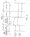
- the optical signal is delivered through an element 1, illustrated as an optical fibre, to a light receiving surface 2 of a semiconductor body 3.
- the semiconductor body 3 has an emitter region 4 of a wider band gap semiconductor material than the base region.
- the region 4 forms an emitter-base p-n junction 5 with a graded band gap base region 6 wherein the grading is from a wider band gap at the interface 5 to a narrower band gap at the base to collector p-n junction 7.
- the collector region 8 is epitaxial at the interface 9 with the substrate 10 and may be provided with a graded band gap for carrier influencing purposes and for lattice accommodation purposes with the substrate 10.
- An external electrical connection 11 is made to the substrate 9, an external electrical connection 12 is made to the surface 2 to transmit the detected electrical signals and an external electrical connection 13 is provided to the base region 6 to drain holes from the base region and for a base contact if electrical signals are being converted.
- the band energy diagram correlated with the regions of the device of FIG. 1.
- the wide band gap coupled with the smaller band gap in the base region provides high emitter injection efficiency.
- the graded band gap in the base region 6 provides a field to accelerate injected carriers to the collection p-n junction and to reduce carrier recombination at dislocations whose density is intolerably large for large lattice mismatch materials.
- the graded band gap in the collector reduces misfit dislocations at the interface 9 with the substrate 10.
- a four-layer structure is provided.
- a wider band gap semiconductor emitter region than the band gap of the base region is employed so that the light will penetrate to the base region without significant absorption yet the injection efficiency of carriers onto the base and potential current gain of the device will be high.
- the material in the base region is selected for optical conversion properties at the selected wavelength and will be provided with a graded band gap so as to produce a strong effective drift field in the base to accelerate carriers toward the collector and to reduce carrier recombination at dislocations where density is intolerably high in large lattice mismatched materials.
- Materials with large lattice mismatches are those which exhibit a change of more than 1% in lattice constant over the entire range of allowed composition change for the material.
- the lattice constants of GaAs and GaP are 5.663 and 5.451, respectively.
- the percent difference in lattice constant for this system is 3.6% and therefore GaAs 1-x P x would be a large lattice mismatch system.
- materials with large dislocation densities, i.e., >10 -10 cm 2 exhibit enhanced carrier recombination at dislocation sites with recombination lifetimes of ⁇ 10 -9 to 10 -10 sec.
- the steeply graded base layer overcomes this limitation. If the base layer contains a high density of dislocations, the drift field produced by grading is sufficient to sweep the carriers across the base-collector junction reducing the recombination by the mechanism involving dislocation sites.
- the transit time for a carrier transversing a 1 ⁇ graded base at a velocity of ⁇ 10 sec is 10 - 11 sec.
- the dislocation recombination lifetime is about 10 -9 to 10 - 10
- the ratio of transit time to carrier recombination lifetime is 0.1 to 0.01 which means that 10 to 100 times more carriers will cross the base-collector junction than will recombine at dislocation sites.
- grading composition in both the base and collector region reduces the detrimental effects of lattice mismatch, i.e., grading reduces the dislocation density. Reducing the dislocation density reduces noise due to carrier generation-recombination centres associated with those dislocations.
- the material In the collector region the material varies in composition so as to accommodate lattice differences between the material of the base and a substrate material.
- the structure of the invention will provide strong absorption in the base region for any light for the photon energies between the smallest band gap of the base region and the band gap of the emitter and the effective drift field will be such that electrons will move at something approaching the peak electron velocity of around 5x10 7 centimeters per second with a base transit time of around one picosecond. As a result, for a given base transit time, the gain obtained will be larger than that obtainable without a graded base.
- a preferred embodiment of the invention would involve the delivery of the optical signal by way of an optical fibre and to use selective grading of the ingredients of binary to ternary semiconductors in the base and collector regions to produce the drift field for the carriers and to accommodate the lattice matching with the substrate.
- the optical fibre I would be of a material which would have low absorption at the light wavelength involved.
- the light signal generator is preferably a solid state electrical to light converting device such as a laser.
- In,Ga In,Ga
- InP InP
- Examples of optical fibre materials suitable for operation at this wavelength are Si0 2 , Ge0 2 and a glassy mixture of germanium and silicon oxides.
- the optimum wavelength is somewhat influenced by the length of the link between the signal generator and the detector. The optimum wavelength for low absorption criteria will be less essential at short link lengths.
- the speed and sensitivity to the light delivered by the fibre 1 will be the main considerations. It is generally always desirable to have a semiconductor material with a low density of defects in order to reduce leakage currents and resulting noise.
- the semiconductor materials involved should have a high band to band absorption coefficient such that much of the light delivered by the fibre through the surface 2 can be absorbed in a base layer 6 which is of the order of 0.25 to 1 micrometers thick.
- FIGS. 1 and 2 While the illustration of FIGS. 1 and 2 is spread out for ease of illustration of the band energy gradients, it will be clear to one skilled in the art that there are semiconductor layer thicknesses which will optimize the light absorption characteristics, the minority carrier transit time, the noise control and the gain of the device.
- Semiconductor materials having a direct energy band gap below the energy of the photons they are absorbing will have higher absorption properties for photon energies.
- the measure is called the absorption coefficient.
- a desirable high absorption coefficient will be 10 4 cm -1 for photon energies of 0.1 electron volts or more greater than the band gap.
- Suitable direct band gap materials will include many of the III-V intermetallic semiconductors such as GaAs, InP, GaSb, InAs, InSb and their alloys.
- the contact 12 should be able to penetrate through the emitter region 4 to region 6 in which the absorption is to take place without first being significantly absorbed in any contacting layer.
- the contact layer material it is desirable that where the contact 12 is a layer that is transparent to the light involved it is preferable that the contact layer material have a larger band gap energy than the wave amplitude of the light.
- the region 4 will be of GaAlAs which has a band gap of about 1.7 electron volts (eV). Since the band gap of the GaAIAs will be larger than 1.4 eV which is the band gap of the GaAs base region 6 at the interface 5 so that the injection efficiency and potential current gain will be high.
- the lattice spacing of Ga 1-x Al x As is matched to that of GaAs in order to minimize the formation of defects which may act as recombination centres.
- a third ingredient, In is progressively introduced producing the semiconductor Ga In As with x progressively increasing so that a narrower band gap is produced at the base to collector p-n junction 7.
- the variation of the crystal composition is employed for band gap and lattice spacing adjustment and appropriate impurity concentration is introduced to provide the desired conductivity type.
- the structure will provide strong absorption in the base region for any light with a photon energy between 0.4 and 1.7 electron volts which translates to a wavelength of between 0.7 and 3 micrometers.
- An effective drift field in the base for a base that is 0.5 to 1 micrometer wide will be roughly 10 4 volts per centimeter. With such a field electrons produced will move at something approaching peak electron velocity which is in the vicinity of 5x10 7 centimeters per second and thus will have a transit time of about 1 picosecond. For a response time of 10 -10 seconds, the device could have a gain of " 100.
- a lattice spacing adjustment may be made by progressively decreasing x which is to decrease the quantity of the ingredient In so as to return to GaAs at interface 9 with a substrate which may be n-conductivity type GaAs.
- GaAlAs As the emitter material and GaInAs as the base-collector material
- IR infrared
- AlSb will serve as the emitter material, with a band gap of 1.6 eV
- Ga 1-x In x Sb will serve as the base-collector material, with a band gap of 0.18 to .7 eV.
- Ga 0.9 In 0.1 Sb can be lattice matched to AlSb and since the band gap of Ga 1-x In x Sb decreases with increasing x, a substrate of GaSb is satisfactory.
- Table I there is provided an illustrative system of a list of various emitter, base-collector and substrate materials which can be used in the practice of this invention.
- graded intermetallic semiconductor alloys permits the tailoring of the properties of the semiconductor in various regions without obtaining a high density of misfit dislocations in spite of a significant lattice mismatch between the various binary semiconductors.
- optical signal detection wherein through a combination of materials selection and of grading a third ingredient into a binary semiconductor optimum optical and structural properties are achieved.
Abstract
Description
- The invention relates to a semiconductor device and a method of forming thereof.
- The technical field of the invention is in the transmission and detection of signals in a semiconductor device wherein internal losses of carriers produced by the signal are minimized within the device. Where the signals are in the optical range, the semiconductor device may be optimized for the system in which it operates. As an illustration, it is desirable for optical signals to perform the conversion at an optical signal wavelength at which the absorption during transmission of the optical signal is very low. However, in optical signal conversion, there are limitations on efficiency by the available light output frequencies of the signal generating equipment, by the attenuation of the light signal by the transmission medium and by the detector which re-converts the optical signal.
- Most work in this field has been directed to the conversion of electrical to optical signals, transmission in air or along quartz based optical fibre materials and reconversion of the optical signal to an electrical signal. As the art is developing, there are advantages in being able to have flexibility in optimizing various aspects of the system.
- It has been known that photodetectors having a rapid response time and sensitivity in the wavelength region of around 1 micron or 1 to 1.4 electron volts are desirable and that these par; meters can be somewhat achieved by having a photodetector with a wide band gap emitter region. Such a structure is shown in U.S. Patent 4,122,476.
- The material InAs has been shown to be a good detector material for wavelengths above .86 micrometers as described in U.S. Patent 4,096,511.
- In general semiconductor practice, the advantages of providing a wide band gap emitter together with a gradient field in the crystal by doping to enhance carrier transport is illustratively described in U.S. Patent 3,081,370.
- According to the invention there is provided a semiconductor device comprising emitter, base and collector regions, characterised in that said emitter region has an energy gap of a first magnitude and forms a first junction with a base region having an energy gap of a second magnitude narrower than said emitter energy gap, said collector region forming a second junction with said base region and said base energy gap decreasing with distance from said first junction to said second junction.
- Further according to the invention there is provided a method of forming a semiconductor device characterised in that the method comprises the steps of providing a substrate layer of n conductivity type monocrystalline AB semiconductor material having two essentially parallel broad area surfaces, forming on a first said broad area surface to be exposed to an optical signal an epitaxial collector layer of A1xCxB wherein x increases with distance from said substrate layer, forming on said collector layer an epitaxial base layer forming a base-collector p-n junction with said base layer, said base layer being of AlxCxB semiconductor material wherein x decreases with distance from said p-n junction, forming an emitter epitaxial layer on said base layer at an emitter-base p-n junction, said emitter layer being of A1xDxB semiconductor material having a higher band gap and lattice matched to said base semiconductor material at said emitter-base p-n junction, and applying an electrical contact to each said substrate, said base and said emitter layers.
- FIG. 1 is a schematic illustration of the regions of a semiconductor device embodying the invention.
- FIG. 2 is a dimensionally correlated energy diagram for the device of FIG. 1.
- The invention involves a signal conversion semiconductor structure wherein through the use of layers of multiple elemental semiconductor materials with common elements, signal transfer gains, lattice mismatch accommodation and carrier transport gains are achieved. The variation of elements provides lattice accommodation which minimizes carrier traps due to dislocations and a graded band gap which due to the accelerating effect on the carriers minimizes the effect of any dislocation carrier traps that do occur.
- The structure and advantages will be explained in connection with the conversion of optical signals although in the light of the principles set forth, use of the structure of the invention for electrical signal conversion will be readily apparent.
- Referring to FIG. 1, the optical signal is delivered through an element 1, illustrated as an optical fibre, to a light receiving surface 2 of a semiconductor body 3. The semiconductor body 3 has an emitter region 4 of a wider band gap semiconductor material than the base region. The region 4 forms an emitter-
base p-n junction 5 with a graded bandgap base region 6 wherein the grading is from a wider band gap at theinterface 5 to a narrower band gap at the base to collector p-n junction 7. Thecollector region 8 is epitaxial at the interface 9 with thesubstrate 10 and may be provided with a graded band gap for carrier influencing purposes and for lattice accommodation purposes with thesubstrate 10. An externalelectrical connection 11 is made to the substrate 9, an externalelectrical connection 12 is made to the surface 2 to transmit the detected electrical signals and an externalelectrical connection 13 is provided to thebase region 6 to drain holes from the base region and for a base contact if electrical signals are being converted. - Referring to FIG. 2, there is shown the band energy diagram correlated with the regions of the device of FIG. 1. In the emitter region 4 the wide band gap coupled with the smaller band gap in the base region provides high emitter injection efficiency. The graded band gap in the
base region 6 provides a field to accelerate injected carriers to the collection p-n junction and to reduce carrier recombination at dislocations whose density is intolerably large for large lattice mismatch materials. In certain embodiments, the graded band gap in the collector reduces misfit dislocations at the interface 9 with thesubstrate 10. - A four-layer structure is provided. A wider band gap semiconductor emitter region than the band gap of the base region is employed so that the light will penetrate to the base region without significant absorption yet the injection efficiency of carriers onto the base and potential current gain of the device will be high.
- The material in the base region is selected for optical conversion properties at the selected wavelength and will be provided with a graded band gap so as to produce a strong effective drift field in the base to accelerate carriers toward the collector and to reduce carrier recombination at dislocations where density is intolerably high in large lattice mismatched materials.
- Materials with large lattice mismatches are those which exhibit a change of more than 1% in lattice constant over the entire range of allowed composition change for the material. For example, the lattice constants of GaAs and GaP are 5.663 and 5.451, respectively. Thus, the percent difference in lattice constant for this system is 3.6% and therefore GaAs1-xPxwould be a large lattice mismatch system. It is known that materials with large dislocation densities, i.e., >10 -10 cm2 exhibit enhanced carrier recombination at dislocation sites with recombination lifetimes of ≈ 10-9 to 10-10 sec. It is also known that materials with a large lattice mismatch, e.g., GaAs1-xPx exhibit enhanced dislocation type carrier recombination especially for material grown on lattice mismatched substrates, e. g. , GaAs.
- In this invention, the steeply graded base layer overcomes this limitation. If the base layer contains a high density of dislocations, the drift field produced by grading is sufficient to sweep the carriers across the base-collector junction reducing the recombination by the mechanism involving dislocation sites. For example, the transit time for a carrier transversing a 1µ graded base at a velocity of ≈ 10 sec is 10 -11 sec. The dislocation recombination lifetime is about 10-9 to 10 -10 Thus, the ratio of transit time to carrier recombination lifetime is 0.1 to 0.01 which means that 10 to 100 times more carriers will cross the base-collector junction than will recombine at dislocation sites.
- In addition, grading composition in both the base and collector region reduces the detrimental effects of lattice mismatch, i.e., grading reduces the dislocation density. Reducing the dislocation density reduces noise due to carrier generation-recombination centres associated with those dislocations.
- In the collector region the material varies in composition so as to accommodate lattice differences between the material of the base and a substrate material.
- The structure of the invention will provide strong absorption in the base region for any light for the photon energies between the smallest band gap of the base region and the band gap of the emitter and the effective drift field will be such that electrons will move at something approaching the peak electron velocity of around 5x10⁷ centimeters per second with a base transit time of around one picosecond. As a result, for a given base transit time, the gain obtained will be larger than that obtainable without a graded base.
- A preferred embodiment of the invention would involve the delivery of the optical signal by way of an optical fibre and to use selective grading of the ingredients of binary to ternary semiconductors in the base and collector regions to produce the drift field for the carriers and to accommodate the lattice matching with the substrate. In such a system, the optical fibre I would be of a material which would have low absorption at the light wavelength involved. The light signal generator is preferably a solid state electrical to light converting device such as a laser.
- A local minimum in light absorption occurs at a 1.3 micrometer wavelength. There are available (In,Ga) (As,P) InP lasers which radiate at such wavelengths. It has also been found that there is a better absorption band around 1.59 to 1.60 micrometers and tailored light sources coupled with optical fibres operating in this region will produce less loss. Examples of optical fibre materials suitable for operation at this wavelength are Si02, Ge02 and a glassy mixture of germanium and silicon oxides. The optimum wavelength is somewhat influenced by the length of the link between the signal generator and the detector. The optimum wavelength for low absorption criteria will be less essential at short link lengths.
- In the body 3 of the detector structure of the invention, the speed and sensitivity to the light delivered by the fibre 1 will be the main considerations. It is generally always desirable to have a semiconductor material with a low density of defects in order to reduce leakage currents and resulting noise.
- The semiconductor materials involved should have a high band to band absorption coefficient such that much of the light delivered by the fibre through the surface 2 can be absorbed in a
base layer 6 which is of the order of 0.25 to 1 micrometers thick. - While the illustration of FIGS. 1 and 2 is spread out for ease of illustration of the band energy gradients, it will be clear to one skilled in the art that there are semiconductor layer thicknesses which will optimize the light absorption characteristics, the minority carrier transit time, the noise control and the gain of the device.
- Semiconductor materials having a direct energy band gap below the energy of the photons they are absorbing will have higher absorption properties for photon energies. The measure is called the absorption coefficient. A desirable high absorption coefficient will be104cm-1 for photon energies of 0.1 electron volts or more greater than the band gap. Suitable direct band gap materials will include many of the III-V intermetallic semiconductors such as GaAs, InP, GaSb, InAs, InSb and their alloys. With respect to the

contact 12, the light should be able to penetrate through the emitter region 4 toregion 6 in which the absorption is to take place without first being significantly absorbed in any contacting layer. Thus, it is desirable that where thecontact 12 is a layer that is transparent to the light involved it is preferable that the contact layer material have a larger band gap energy than the wave amplitude of the light. - Referring to FIG. 1, for a silicon based optical fibre such as quartz, the region 4 will be of GaAlAs which has a band gap of about 1.7 electron volts (eV). Since the band gap of the GaAIAs will be larger than 1.4 eV which is the band gap of the GaAs
base region 6 at theinterface 5 so that the injection efficiency and potential current gain will be high. At theinterface 5, the lattice spacing of Ga1-xAlxAs is matched to that of GaAs in order to minimize the formation of defects which may act as recombination centres. In theregion 6, a third ingredient, In, is progressively introduced producing the semiconductor Ga In As with x progressively increasing so that a narrower band gap is produced at the base to collector p-n junction 7. In theregions - The structure will provide strong absorption in the base region for any light with a photon energy between 0.4 and 1.7 electron volts which translates to a wavelength of between 0.7 and 3 micrometers. An effective drift field in the base for a base that is 0.5 to 1 micrometer wide will be roughly 104 volts per centimeter. With such a field electrons produced will move at something approaching peak electron velocity which is in the vicinity of 5x10⁷ centimeters per second and thus will have a transit time of about 1 picosecond. For a response time of 10-10 seconds, the device could have a gain of "100.
- In the
collector region 8, if needed, a lattice spacing adjustment may be made by progressively decreasing x which is to decrease the quantity of the ingredient In so as to return to GaAs at interface 9 with a substrate which may be n-conductivity type GaAs. - While the above discussion has been directed toward the use of GaAlAs as the emitter material and GaInAs as the base-collector material, there are other exemplary systems available. For example, for infrared (IR) signal detection, AlSb will serve as the emitter material, with a band gap of 1.6 eV and Ga1-xInxSb will serve as the base-collector material, with a band gap of 0.18 to .7 eV. Since Ga0.9In0.1Sb can be lattice matched to AlSb and since the band gap of Ga1-xInxSb decreases with increasing x, a substrate of GaSb is satisfactory.
- In Table I there is provided an illustrative system of a list of various emitter, base-collector and substrate materials which can be used in the practice of this invention.

- Thus, the use of graded intermetallic semiconductor alloys permits the tailoring of the properties of the semiconductor in various regions without obtaining a high density of misfit dislocations in spite of a significant lattice mismatch between the various binary semiconductors.
- What has been described is optical signal detection wherein through a combination of materials selection and of grading a third ingredient into a binary semiconductor optimum optical and structural properties are achieved.
Claims (6)
Applications Claiming Priority (2)
| Application Number | Priority Date | Filing Date | Title |
|---|---|---|---|
| US06/393,923 US4518979A (en) | 1982-06-30 | 1982-06-30 | Semiconductor transistor with graded base and collector |
| US393923 | 1989-08-16 |
Publications (3)
| Publication Number | Publication Date |
|---|---|
| EP0097767A2 true EP0097767A2 (en) | 1984-01-11 |
| EP0097767A3 EP0097767A3 (en) | 1986-04-30 |
| EP0097767B1 EP0097767B1 (en) | 1989-08-09 |
Family
ID=23556804
Family Applications (1)
| Application Number | Title | Priority Date | Filing Date |
|---|---|---|---|
| EP83102549A Expired EP0097767B1 (en) | 1982-06-30 | 1983-03-15 | A semiconductor device |
Country Status (4)
| Country | Link |
|---|---|
| US (1) | US4518979A (en) |
| EP (1) | EP0097767B1 (en) |
| JP (1) | JPS599979A (en) |
| DE (1) | DE3380385D1 (en) |
Cited By (2)
| Publication number | Priority date | Publication date | Assignee | Title |
|---|---|---|---|---|
| EP0453945A1 (en) * | 1990-04-18 | 1991-10-30 | Fujitsu Limited | Heterojunction bipolar transistor |
| US5150186A (en) * | 1991-03-06 | 1992-09-22 | Micron Technology, Inc. | CMOS output pull-up driver |
Families Citing this family (11)
| Publication number | Priority date | Publication date | Assignee | Title |
|---|---|---|---|---|
| US4794440A (en) * | 1983-05-25 | 1988-12-27 | American Telephone And Telegraph Company, At&T Bell Laboratories | Heterojunction bipolar transistor |
| US5214297A (en) * | 1984-11-19 | 1993-05-25 | Fujitsu Limited | High-speed semiconductor device |
| JPH0669222A (en) * | 1992-08-17 | 1994-03-11 | Matsushita Electric Ind Co Ltd | Hetero-junction bipolar transistor and its production |
| JP2771423B2 (en) * | 1993-05-20 | 1998-07-02 | 日本電気株式会社 | Bipolar transistor |
| US5576559A (en) * | 1994-11-01 | 1996-11-19 | Intevac, Inc. | Heterojunction electron transfer device |
| FR2780203B1 (en) * | 1998-06-23 | 2003-07-04 | Thomson Csf | QUANTUM WELL DETECTOR WITH PHOTOEXCITED ELECTRON STORAGE LAYER |
| US6847060B2 (en) * | 2000-11-27 | 2005-01-25 | Kopin Corporation | Bipolar transistor with graded base layer |
| US7345327B2 (en) | 2000-11-27 | 2008-03-18 | Kopin Corporation | Bipolar transistor |
| JP2004521485A (en) * | 2000-11-27 | 2004-07-15 | コピン コーポレーション | Bipolar transistor with lattice matched base layer |
| US6800879B2 (en) * | 2001-01-08 | 2004-10-05 | Kopin Corporation | Method of preparing indium phosphide heterojunction bipolar transistors |
| US7566948B2 (en) * | 2004-10-20 | 2009-07-28 | Kopin Corporation | Bipolar transistor with enhanced base transport |
Citations (2)
| Publication number | Priority date | Publication date | Assignee | Title |
|---|---|---|---|---|
| US4096511A (en) * | 1971-11-29 | 1978-06-20 | Philip Gurnell | Photocathodes |
| DE2847451A1 (en) * | 1978-11-02 | 1980-06-04 | Licentia Gmbh | Semiconductor drift transistor with different accelerations of charge - has tapered gap between valency band and conducting band in semiconductor zone |
Family Cites Families (9)
| Publication number | Priority date | Publication date | Assignee | Title |
|---|---|---|---|---|
| US3081370A (en) * | 1961-07-17 | 1963-03-12 | Raytheon Co | Solar cells |
| US3995303A (en) * | 1975-06-05 | 1976-11-30 | Bell Telephone Laboratories, Incorporated | Growth and operation of a step-graded ternary III-V heterojunction p-n diode photodetector |
| US4075651A (en) * | 1976-03-29 | 1978-02-21 | Varian Associates, Inc. | High speed fet employing ternary and quarternary iii-v active layers |
| US4122476A (en) * | 1976-11-22 | 1978-10-24 | International Business Machines Corporation | Semiconductor heterostructure |
| JPS53135290A (en) * | 1977-04-28 | 1978-11-25 | Uni Konechikatsuto | Improved hetero junction and method of producing same |
| US4160258A (en) * | 1977-11-18 | 1979-07-03 | Bell Telephone Laboratories, Incorporated | Optically coupled linear bilateral transistor |
| JPS561578A (en) * | 1979-06-18 | 1981-01-09 | Shunpei Yamazaki | Manufacture of semiconductor device |
| US4275404A (en) * | 1979-10-05 | 1981-06-23 | Bell Telephone Laboratories, Incorporated | Monolithic opto-isolator |
| US4383269A (en) * | 1980-09-19 | 1983-05-10 | Bell Telephone Laboratories, Incorporated | Graded bandgap photodetector |
-
1982
- 1982-06-30 US US06/393,923 patent/US4518979A/en not_active Expired - Lifetime
-
1983
- 1983-03-15 DE DE8383102549T patent/DE3380385D1/en not_active Expired
- 1983-03-15 EP EP83102549A patent/EP0097767B1/en not_active Expired
- 1983-04-20 JP JP58068508A patent/JPS599979A/en active Granted
Patent Citations (2)
| Publication number | Priority date | Publication date | Assignee | Title |
|---|---|---|---|---|
| US4096511A (en) * | 1971-11-29 | 1978-06-20 | Philip Gurnell | Photocathodes |
| DE2847451A1 (en) * | 1978-11-02 | 1980-06-04 | Licentia Gmbh | Semiconductor drift transistor with different accelerations of charge - has tapered gap between valency band and conducting band in semiconductor zone |
Non-Patent Citations (1)
| Title |
|---|
| IBM TECHNICAL DISCLOSURE BULLETIN, vol. 22, no. 8B, January 1980, page 3875, New York, US; H.J. HOVEL: "Graded bandgap heterojunction bipolar transistor" * |
Cited By (2)
| Publication number | Priority date | Publication date | Assignee | Title |
|---|---|---|---|---|
| EP0453945A1 (en) * | 1990-04-18 | 1991-10-30 | Fujitsu Limited | Heterojunction bipolar transistor |
| US5150186A (en) * | 1991-03-06 | 1992-09-22 | Micron Technology, Inc. | CMOS output pull-up driver |
Also Published As
| Publication number | Publication date |
|---|---|
| EP0097767A3 (en) | 1986-04-30 |
| JPS6329423B2 (en) | 1988-06-14 |
| DE3380385D1 (en) | 1989-09-14 |
| EP0097767B1 (en) | 1989-08-09 |
| US4518979A (en) | 1985-05-21 |
| JPS599979A (en) | 1984-01-19 |
Similar Documents
| Publication | Publication Date | Title |
|---|---|---|
| US3821777A (en) | Avalanche photodiode | |
| Pearsall et al. | Avalanche gain in Ge x Si 1-x/Si infrared waveguide detectors | |
| US4383269A (en) | Graded bandgap photodetector | |
| EP0097767B1 (en) | A semiconductor device | |
| US4119994A (en) | Heterojunction and process for fabricating same | |
| EP0159544B1 (en) | Avalanche photodiode and its manufacturing method | |
| US6326654B1 (en) | Hybrid ultraviolet detector | |
| Capasso | New multilayer and graded gap optoelectronic and high speed devices by band gap engineering | |
| CA1192976A (en) | Majority carrier photodetector | |
| Stillman et al. | Long-wavelength (1.3-to 1.6-µm) detectors for fiber-optical communications | |
| US4160258A (en) | Optically coupled linear bilateral transistor | |
| EP0304048B1 (en) | A planar type heterostructure avalanche photodiode | |
| Diadiuk et al. | Low dark-current, high gain GaInAs/InP avalanche photodetectors | |
| Jang et al. | Metamorphic graded bandgap InGaAs-InGaAlAs-InAlAs double heterojunction PiIN photodiodes | |
| EP0115591B1 (en) | Photodiode and photodetector comprising an integrated series of photodiodes | |
| EP0113074B1 (en) | Method of logically combining optical signals | |
| Capasso | New heterojunction devices by band-gap engineering | |
| Yeats et al. | Long‐wavelength InGaAsP avalanche photodiodes | |
| GB2083699A (en) | Phototransistor having an emitter-base heterojunction | |
| JPS63955B2 (en) | ||
| Kim et al. | Barrier height enhancement of InP-based n-Ga0. 47In0. 53As Schottky-barrier diodes grown by molecular beam epitaxy | |
| JPS63108782A (en) | Semiconductor photodetector | |
| JP2703167B2 (en) | Light receiving element and method of manufacturing the same | |
| JPH0437591B2 (en) | ||
| Ashley et al. | Diffusion lengths in amphoteric GaAs heteroface solar cells |
Legal Events
| Date | Code | Title | Description |
|---|---|---|---|
| PUAI | Public reference made under article 153(3) epc to a published international application that has entered the european phase |
Free format text: ORIGINAL CODE: 0009012 |
|
| AK | Designated contracting states |
Designated state(s): DE FR GB |
|
| 17P | Request for examination filed |
Effective date: 19840426 |
|
| PUAL | Search report despatched |
Free format text: ORIGINAL CODE: 0009013 |
|
| AK | Designated contracting states |
Kind code of ref document: A3 Designated state(s): DE FR GB |
|
| 17Q | First examination report despatched |
Effective date: 19880217 |
|
| GRAA | (expected) grant |
Free format text: ORIGINAL CODE: 0009210 |
|
| AK | Designated contracting states |
Kind code of ref document: B1 Designated state(s): DE FR GB |
|
| REF | Corresponds to: |
Ref document number: 3380385 Country of ref document: DE Date of ref document: 19890914 |
|
| ET | Fr: translation filed | ||
| PLBE | No opposition filed within time limit |
Free format text: ORIGINAL CODE: 0009261 |
|
| STAA | Information on the status of an ep patent application or granted ep patent |
Free format text: STATUS: NO OPPOSITION FILED WITHIN TIME LIMIT |
|
| 26N | No opposition filed | ||
| PGFP | Annual fee paid to national office [announced via postgrant information from national office to epo] |
Ref country code: GB Payment date: 19920210 Year of fee payment: 10 |
|
| PGFP | Annual fee paid to national office [announced via postgrant information from national office to epo] |
Ref country code: FR Payment date: 19920227 Year of fee payment: 10 |
|
| PGFP | Annual fee paid to national office [announced via postgrant information from national office to epo] |
Ref country code: DE Payment date: 19920321 Year of fee payment: 10 |
|
| PG25 | Lapsed in a contracting state [announced via postgrant information from national office to epo] |
Ref country code: GB Effective date: 19930315 |
|
| GBPC | Gb: european patent ceased through non-payment of renewal fee |
Effective date: 19930315 |
|
| PG25 | Lapsed in a contracting state [announced via postgrant information from national office to epo] |
Ref country code: FR Effective date: 19931130 |
|
| PG25 | Lapsed in a contracting state [announced via postgrant information from national office to epo] |
Ref country code: DE Effective date: 19931201 |
|
| REG | Reference to a national code |
Ref country code: FR Ref legal event code: ST |