EP0103138A2 - Semiconductor rectifier diode - Google Patents
Semiconductor rectifier diode Download PDFInfo
- Publication number
- EP0103138A2 EP0103138A2 EP83107656A EP83107656A EP0103138A2 EP 0103138 A2 EP0103138 A2 EP 0103138A2 EP 83107656 A EP83107656 A EP 83107656A EP 83107656 A EP83107656 A EP 83107656A EP 0103138 A2 EP0103138 A2 EP 0103138A2
- Authority
- EP
- European Patent Office
- Prior art keywords
- layer
- impurity concentration
- rectifier diode
- base layer
- semiconductor rectifier
- Prior art date
- Legal status (The legal status is an assumption and is not a legal conclusion. Google has not performed a legal analysis and makes no representation as to the accuracy of the status listed.)
- Granted
Links
- 239000004065 semiconductor Substances 0.000 title claims abstract description 38
- 239000012535 impurity Substances 0.000 claims abstract description 60
- 230000000903 blocking effect Effects 0.000 claims description 18
- 239000000758 substrate Substances 0.000 claims description 9
- 238000011084 recovery Methods 0.000 abstract description 22
- 230000004044 response Effects 0.000 abstract description 6
- 239000010410 layer Substances 0.000 description 124
- 230000009467 reduction Effects 0.000 description 9
- 239000000969 carrier Substances 0.000 description 7
- 230000003247 decreasing effect Effects 0.000 description 6
- 238000004519 manufacturing process Methods 0.000 description 6
- 230000004888 barrier function Effects 0.000 description 5
- 238000009792 diffusion process Methods 0.000 description 4
- VYPSYNLAJGMNEJ-UHFFFAOYSA-N silicon dioxide Inorganic materials O=[Si]=O VYPSYNLAJGMNEJ-UHFFFAOYSA-N 0.000 description 4
- WSNMPAVSZJSIMT-UHFFFAOYSA-N COc1c(C)c2COC(=O)c2c(O)c1CC(O)C1(C)CCC(=O)O1 Chemical class COc1c(C)c2COC(=O)c2c(O)c1CC(O)C1(C)CCC(=O)O1 WSNMPAVSZJSIMT-UHFFFAOYSA-N 0.000 description 3
- 229910052681 coesite Inorganic materials 0.000 description 3
- 229910052906 cristobalite Inorganic materials 0.000 description 3
- 230000000694 effects Effects 0.000 description 3
- 238000000034 method Methods 0.000 description 3
- 229910052682 stishovite Inorganic materials 0.000 description 3
- 229910052905 tridymite Inorganic materials 0.000 description 3
- ZOXJGFHDIHLPTG-UHFFFAOYSA-N Boron Chemical compound [B] ZOXJGFHDIHLPTG-UHFFFAOYSA-N 0.000 description 2
- XUIMIQQOPSSXEZ-UHFFFAOYSA-N Silicon Chemical compound [Si] XUIMIQQOPSSXEZ-UHFFFAOYSA-N 0.000 description 2
- 229910052796 boron Inorganic materials 0.000 description 2
- 230000015556 catabolic process Effects 0.000 description 2
- 230000001143 conditioned effect Effects 0.000 description 2
- 238000013461 design Methods 0.000 description 2
- 230000007935 neutral effect Effects 0.000 description 2
- 229910052710 silicon Inorganic materials 0.000 description 2
- 239000010703 silicon Substances 0.000 description 2
- 229910000789 Aluminium-silicon alloy Inorganic materials 0.000 description 1
- OAICVXFJPJFONN-UHFFFAOYSA-N Phosphorus Chemical compound [P] OAICVXFJPJFONN-UHFFFAOYSA-N 0.000 description 1
- 238000013459 approach Methods 0.000 description 1
- 238000005229 chemical vapour deposition Methods 0.000 description 1
- 230000007547 defect Effects 0.000 description 1
- 230000005684 electric field Effects 0.000 description 1
- 238000010438 heat treatment Methods 0.000 description 1
- 238000005259 measurement Methods 0.000 description 1
- 238000012986 modification Methods 0.000 description 1
- 230000004048 modification Effects 0.000 description 1
- 229910021421 monocrystalline silicon Inorganic materials 0.000 description 1
- 238000005036 potential barrier Methods 0.000 description 1
- 239000000377 silicon dioxide Substances 0.000 description 1
- 239000002356 single layer Substances 0.000 description 1
- 230000007704 transition Effects 0.000 description 1
Images


Classifications
-
- H—ELECTRICITY
- H01—ELECTRIC ELEMENTS
- H01L—SEMICONDUCTOR DEVICES NOT COVERED BY CLASS H10
- H01L29/00—Semiconductor devices adapted for rectifying, amplifying, oscillating or switching, or capacitors or resistors with at least one potential-jump barrier or surface barrier, e.g. PN junction depletion layer or carrier concentration layer; Details of semiconductor bodies or of electrodes thereof ; Multistep manufacturing processes therefor
- H01L29/66—Types of semiconductor device ; Multistep manufacturing processes therefor
- H01L29/86—Types of semiconductor device ; Multistep manufacturing processes therefor controllable only by variation of the electric current supplied, or only the electric potential applied, to one or more of the electrodes carrying the current to be rectified, amplified, oscillated or switched
- H01L29/861—Diodes
-
- H—ELECTRICITY
- H01—ELECTRIC ELEMENTS
- H01L—SEMICONDUCTOR DEVICES NOT COVERED BY CLASS H10
- H01L29/00—Semiconductor devices adapted for rectifying, amplifying, oscillating or switching, or capacitors or resistors with at least one potential-jump barrier or surface barrier, e.g. PN junction depletion layer or carrier concentration layer; Details of semiconductor bodies or of electrodes thereof ; Multistep manufacturing processes therefor
- H01L29/02—Semiconductor bodies ; Multistep manufacturing processes therefor
- H01L29/06—Semiconductor bodies ; Multistep manufacturing processes therefor characterised by their shape; characterised by the shapes, relative sizes, or dispositions of the semiconductor regions ; characterised by the concentration or distribution of impurities within semiconductor regions
- H01L29/0684—Semiconductor bodies ; Multistep manufacturing processes therefor characterised by their shape; characterised by the shapes, relative sizes, or dispositions of the semiconductor regions ; characterised by the concentration or distribution of impurities within semiconductor regions characterised by the shape, relative sizes or dispositions of the semiconductor regions or junctions between the regions
- H01L29/0688—Semiconductor bodies ; Multistep manufacturing processes therefor characterised by their shape; characterised by the shapes, relative sizes, or dispositions of the semiconductor regions ; characterised by the concentration or distribution of impurities within semiconductor regions characterised by the shape, relative sizes or dispositions of the semiconductor regions or junctions between the regions characterised by the particular shape of a junction between semiconductor regions
-
- H—ELECTRICITY
- H01—ELECTRIC ELEMENTS
- H01L—SEMICONDUCTOR DEVICES NOT COVERED BY CLASS H10
- H01L29/00—Semiconductor devices adapted for rectifying, amplifying, oscillating or switching, or capacitors or resistors with at least one potential-jump barrier or surface barrier, e.g. PN junction depletion layer or carrier concentration layer; Details of semiconductor bodies or of electrodes thereof ; Multistep manufacturing processes therefor
- H01L29/02—Semiconductor bodies ; Multistep manufacturing processes therefor
- H01L29/36—Semiconductor bodies ; Multistep manufacturing processes therefor characterised by the concentration or distribution of impurities in the bulk material
Abstract
Description
- The present invention relates to a semiconductor device, and in particular to a semiconductor rectifier diode.
- In recent years, IC's and LSI's have been rapidly introduced into a computer and associated various terminal units or various system apparatuses. A low voltage stabilized DC power supply is demanded to feed such an apparatus. Among-various methods for obtaining a low voltage stabilized DC power supply from the commercial AC power source, the switching regulator system is excellent in its small size and high efficiency.
- Properties demanded for a rectifier diode to be used in the above described power supply are low loss, high stability and quick response. Diodes heretofore known did not fully satisfy these requirements. For example, a Shottky barrier diode described in the Japanese Patent Application Laid-open No. 107272/80 has a large reverse leak current and a rather large thermal instability.
- A p-i-n junction diode does not fully satisfy the low loss requirement. It has been proposed to make the p-type layer or n-type layer of a p-i-n diode extremely thin to improve the low-loss property as described in IEEE Transactions on Electron Devices, Vol. ED-23, No. 8, August 1976, p.p. 945 to 949. Similarly to the Schottky barrier diode, however, this approach does not always facilitate production of the p-i-n diode and has often brought about a difficulty in obtaining high fabrication yield due to variation in blocking voltage.
- An object of the present invention is to provide a semiconductor rectifier diode wherein the above described drawbacks are obviated. In other words, the object of the present invention is to provide a semiconductor rectifier diode which meets low loss, high stability and quick response requirements and is easily produced.
- Another object of the present invention is to provide a semiconductor rectifier diode having a soft reverse recovery characteristic.
- One feature of the semiconductor rectifier diode according to the present invention for attaining the above described object is that the diode has a first emitter layer of a first conductivity type, a base layer of a second conductivity type which is adjacent to the first emitter layer, and a second emitter layer of the second conductivity type which is adjacent to the base layer, and the first emitter layer is composed of a first portion and second portions surrounding the first portion, the second portions being formed deeper than the first portion and having a higher impurity concentration as compared with the first portions. Here, the emitter layer refers to a region wherein the impurity concentration is higher than the carrier concentration at the time of its forward operation. The base layer refers to a region wherein the impurity concentration is lower than the carrier concentration at the time of its forward operation. Owing to such a structure, it becomes possible to realize a semiconductor rectifier diode which excels a p-i-n junction diode in low loss and quick response properties and excels a Schottky barrier diode in stability, high voltage blocking capability and fabrication readiness.
- Another feature of a semiconductor rectifier diode according to the present invention is that the distance between second portions across a first portion in the first emitter layer, i.e., the width of the first portion therebetween is set at a sufficient value for pinching off the base region under the first portion by depletion layers extending from p-n junctions between the second portions and the base when a p-n junction existing between the first emitter layer and the base layer is reverse-biased with the rated voltage of the diode. This structure brings about a blocking voltage which is equivalent to that of the p-i-n junction diode.
- Still another feature of a semiconductor rectifier diode according to the present invention is that the impurity concentration in the base region is made to, as a whole, increase with the increase in distance from the p-n junction. Specifically, the base layer is constituted either from a plurality of layer portions respectively having different impurity concentrations or a single layer having an impurity concentration which continuously varies therein. This structure results in a semiconductor rectifier diode having a soft reverse recovery characteristic.
- The present invention will be apparent from the following detailed description taken in conjunction with the accompanying drawings, in which:
- Fig. 1 is a schematic oblique view of an embodiment of a semiconductor rectifier diode according to the present invention;
- Fig. 2 is a plan view of a semiconductor substrate of the device illustrated in Fig. 1;
- Fig. 3 is an enlarged view of the principal part of the device illustrated in Fig. 1;
- Fig. 4 shows the distribution of the impurity concentration within the device illustrated in Fig. 1;
- Fig. 5 shows characteristic curves illustrating the relationship between the width of the first portion of the p-type emitter layer and the forward voltage drop in the device illustrated in Fig. 1;
- Fig. 6 shows characteristic curves illustrating the relationship between the width of the first portion of the p-type emitter layer and the blocking voltage in the device illustrated in Fig. 1;
- Fig. 7 shows characteristic curves illustrating the relationship between the surface impurity concentration of the first portion of the p-type emitter layer and the forward voltage drop in the device illustrated in Fig. 1;
- Fig. 8 shows a characteristic curve illustrating the relationship between the surface impurity concentration of the first portion of the p-type emitter layer and the reverse recovery time in the device illustrated in Fig. 1;
- Fig. 9 shows characteristic curves illustrating the relationship between the surface impurity concentration of the first portion of the p-type emitter layer and the reduction rate of the reverse recovery current in the device illustrated in Fig. 1;
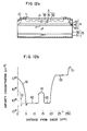
- Fig. 10 is a schematic sectional view of another embodiment of a semiconductor rectifier diode according to the present invention;
- Figs. lla and llb respectively illustrate the structure and the impurity concentration profile of still another embodiment of a semiconductor rectifier diode according to the present invention; and
- Figs. 12a and 12b respectively illustrate the structure and the impurity concentration profile of still another embodiment of a semiconductor rectifier diode according to the present invention.
- Hereafter, embodiments of the present invention will be described in detail by referring to drawings.
- In Fig. 1, Fig. 2 and Fig. 3, a
semiconductor substrate 100 has a pair ofmain surfaces main surfaces type emitter layer 5 composed of an n++-type layer portion 51 which is adjacent to themain surface 102 and an n+-type layer portion 52 which is adjacent to thelayer portion 51 and is lower than thatlayer portion 51 in concentration, an n-type base layer 4 which is adjacent to thelayer 5 and is lower than thelayer 5 in concentration, and a p-type emitter layer 3 which is adjacent to themain surface 101 and is adjacent to thelayer 4 to form a p-n junction Jl. Thus, thesemiconductor substrate 100 has a structure composed of consecutive layers. The n-type base layer 4 is composed of afirst layer portion 41 which is adjacent to thelayer 5 and asecond layer portion 42 which is placed between thelayer portion 41 and thelayer 3 and is lower than theportion 41 in concentration. The p-type emitter layer 3 is composed of afirst portion 31 which is thin in thickness and low in concentration andsecond portions 32 which have a higher concentration than thefirst portion 31 and is formed more deeply than thefirst portion 31. Thefirst portion 31 and thesecond portions 32 and formed in stripe-shape and are alternately arranged so that they face one another lengthwise. On themain surface 101, thefirst portion 31 is surrounded bv thesecond portions 32 as illustrated in Fig. 2. Fig. 1 and Fig. 3 are sectional views viewed from the direction perpendicular to the length of the stripes. Thus, the p-n junction J1 is composed of a first portion J11 formed between theportions portions main surface 102. Symbol II denotes a second laminated structure, each layer of which overlaps with the junction J12 when projected onto themain surface 102. - On a portion of the
main surface 101 whereon the p-n junction is exposed, an Si02 film 10 is formed. On the exposed portion of the p-type emitter layer 3, ananode electrode 1 which is in ohmic contact with the p-type emitter layer 3 is formed. On themain surface 102, acathode electrode 2 which is in ohmic contact with the n-type emitter layer is formed. On the SiO2 film, theanode electrode 1 is extended outward from the end of the exposed portion of the p-n junction J1 to serve as a field plate. - A solid line in Fig. 4 illustrates the distribution of impurity concentrations within the second laminated structure II of the semiconductor substrate taken in a direction which is denoted by x in Fig. 3. In Fig. 4, the distribution of impurity concentrations within the first laminated structure I taken in a direction which is denoted by y in Fig. 3 is also illustrated. For the first laminated structure I, however, only a portion of the distribution which differs from that of the second laminated structure II is illustrated in Fig. 4 by with a broken line.
- A diode of this embodiment may be fabricated by using a well known semiconductor fabrication technique. An example of the fabrication is described in the following.
- At first, on one face of an n -type monocrystalline silicon wafer, an n-type layer and an n -type layer are successively formed by epitaxial growth technique to yield a silicon substrate. Phosphor is diffused selectively from one main surface and entirely from the other main surface. Thus, an n++-type layer 6 which is exposed to a periphery of one
main surface 101 at the chip end and an n++-type layer 51 which is exposed to the othermain surface 102 are formed. Subsequently, boron is selectively diffused from themain surface 101 by using an oxide film as a mask, thesecond portions 32 being formed. From themain surface 101, boron is ion-implanted and subjected to heat treatment to form thefirst portion 31. Onto predetermined portions ofmain surfaces 101 and.102 of the silicon substrate, laminated films made of AlSi, Cr-Ni-Ag or the like are evaporated to form theanode electrode 1 and thecathode electrode 2. The Si02 film 10 is deposited during the above described diffusion process or by the CVD method or the like. - The function and effect of the above described diode will now be described.
- Under a so-called forward bias state wherein a positive voltage is applied to the
anode electrode 1 with respect to thecathode electrode 2, the impurity concentration in thefirst portion 31 in the p-type emitter layer 3 is lower than that in thesecond portion 32 thereof. As a result, the diffusion potential of the first,portion Jli within the p-n junction J1 becomes lower than that of the second portion J12. Accordingly, the main current flows mainly through the first laminated structure I wherein thefirst portion 31 serves as one of the emitters. When the first laminated structure I thus becomes the main current path, minority carriers contribute to operation between thefirst portion 31 and theanode electrode 1 because the diffusion potential is low and thefirst portion 31 is thin. And the barrier between thefirst portion 31 and the anode electrode is not an obstacle to the carrier movement. As a result, the forward voltage may be made smaller than that in the case where the second laminated structure II is the main current path. In addition, the total amount of impurities included in thefirst portion 31 of the p-type emitter layer 3 is less than that included in thesecond portions 32 since thefirst portion 31 of the p-type emitter layer 3 is thinner than thesecond portions 32 thereof and the former has a lower impurity concentration as compared with the latter. Under the forward bias state, therefore, the amount of carriers injected from the p-type emitter layer 3 into the n-type base layer 4 is small. Thus, it becomes possible to reduce the reverse recovery time required for transition from the forward bias state to the reverse bias state. - Under a so-called reverse bias state wherein a negative voltage is applied to the
anode electrode 1 with respect to thecathode electrode 2, a depletion layer formed near the p-n junction J1 extends mainly in the n-type base layer 4 in the vicinity of the second portion J12 due to the difference between the impurity concentration in thesecond portion 32 within the p-type emitter layer 3 and that in the n-type base layer 4. Therefore, thesecond layer portion 42 of the n-type base layer 4 located between the second portiions 32 and under thefirst portion 31 is pinched off by the depletion layer extending from the second portion J12 of the p-n junction. Accordingly, the strength of the electric field in the first portion J11 of the p-n junction is weakened. Since thefirst portion 31 is thin and has a low impurity concentration, the first portion J11 of the p-n junction tends to be easily punched through to the surface by the depletion layer extending in the p-type emitter layer side and therefore has a low blocking voltage. Owing to the depletion layer caused by the existence of thesecond portions 32, however, the voltage is blocked and the first portion J11 is prevented from being punched through. As a result, it becomes possible to obtain a blocking voltage which is equivalent to that obtained when the p-type emitter layer is composed of only thesecond portions 32. - At this time, the depletion layer extending from the second portion J12 of the p-n junction J toward the other
main surface 102,is prevented from further widening beyond the vicinity of the boundary between thefirst layer portion 41 and thesecond layer portion 42 included in the n-type base layer 4 or beyond thefirst layer portion 41. When the diode is switched from the forward conduction state to the reverse blocking state, thefirst layer portion 41 which is filled with injected carriers remains as a neutral region within the n-type base layer 4 even after the depletion layer has been formed. From the time when the reverse current reaches its peak value until the time when the carriers in the neutral region disappear, the reverse current flows while decreasing gradually, whereby the reverse recovery characteristic being softened. The "soft" reverse recovery characteristic means that the reduction rate diR/dt of the reverse current iR after it has reached its peak value is rather small. Should the reverse current decrease rapidly, a large voltage L diR/dt is induced by the inductance L included in the circuit comprising the diode, noises being incurred. - As described above, embodiments of the present invention illustrated in Figs. 1, 2, and 3 yield a semiconductor rectifier diode which excels a conventional junction diode in low loss, quick response and soft recovery properties and excels a Schottky barrier diode in stability and high breakdown voltage properties. The p-
type emitter layer 3 is divided into thefirst portion 31 and thesecond portions 32, and design objectives which are incompatible with each other such as a lowered loss and a raised breakdown voltage are separately achieved by the first and second portions, respectively. Accordingly, the design of the p-type emitter becomes easy. In addition, the blocking voltage is not lowered even if a defect such as a pinhole exists in thefirst portion 31. Thus, the fabrication yield may also be improved. - Fig. 5 shows the dependence of the forward voltage drop upon the width Wch of the
first portion 31 within the diode illustrated in Figs. 1, 2 and 3. Fig. 6 shows the dependence of the blocking voltage upon the width Wch. In these cases, the current density is approximately 60 A/cm2, the thickness Lp of thefirst portion 31 is approximately 2 µm, the thickness of thesecond portion 32 is approximately 5 µm, the thickness of thesecond layer portion 42 existing between the bottom portion of thefirst portion 31 and thefirst layer portion 41 is approximately 6 µm, the thickness of thefirst layer portion 41 is approximately 12 µm, the impurity concentration in thefirst layer portion 41 is approximately 3 x 1015 cm-3, and the surface impurity concentration in thefirst portion 31 taken on themain surface 101 is approximately 5 x 1015 cm-3. Symbols A and O in Fig. 5 and Fig. 6 correspond to impurity concentrations of approximately 3 x 10 13 cm-3 and approximately 1 x 10 14 cm-3 in thesecond layer portion 42, respectively. - As seen from Fig. 5 and Fig. 6, reducing the width of the
first portion 31 from 10 µm to 2 µm raises the blocking voltage by approximately 70 V only at a cost of increase in the forward voltage drop of approximately 0.02 V even when the surface impurity concentration in thefirst portion 31 is as low as approximately 5 x 1015 cm-3 and the thickness thereof is as thin as approximately 2 µm. - The effect of the surface impurity concentration in the
first portion 31 upon the characteristics of the diode in this embodiment will now be described. - Fig. 7 and Fig. 8 respectively illustrate the forward voltage drop and reverse recovery time trr when the thickness Lp of the
first portion 31 is chosen to be 1 µm (represented by Lpl) or 2 µm (represented by Lp2). The forward current density was conditioned to be approximately 60 A/cm2. The reduction rate of the forward current during reverse recovery was conditioned to be approximately 30 A/µs. - Fig. 7 and Fig. 8 indicate that it becomes possible to lower the forward voltage and quicken the reverse recovery by decreasing the thickness of the
first portion 31 to 1 to 2 µm and lowering the surface impurity concentration thereof. For example, when the thickness of the first-portion 31 is 1 to 2 µm and the surface impurity concentration is below 1 x 1016 cm-3, the forward voltage drop is approximately 0.7 V and the reverse recovery time trr is as low as 50 to 60 ns, a diode presenting a low loss and fast response being obtained. As the impurity concentration in thefirst portion 31 is lowered, reverse recovery is quickened because holes injected from thefirst portion 31 into the n-type base layer 4 under the forward bias state are decreased and whereby the amount of stored carriers is decreased. When the impurity concentration in thefirst portion 31 is lowered, the forward voltage is also lowered because the diffusion potential at the p-n junction J11 is lowered. - Fig. 9 shows the reduction rate diR/dt of the reverse recovery current when the thickness Lp of the
first portion 31 is chosen to be approximately 2 µm. The impurity concentration in thesecond layer portion 42 is chosen to be approximately 3 x 1013 cm-3. In Fig. 9, curve A represents the reduction rate when the impurity concentration in thefirst layer portion 41 is approximately 3 x 1015 cm-3. In case of curve B, the impurity concentration in thefirst layer portion 41 is approximately 3 x 1013 cm-3 which is equal to that of thesecond layer portion 42. In this case, the impurity concentration in the n-type base layer 4 is chosen to be uniform in the layer-stacking direction. As the surface impurity concentration in thefirst portion 31 is decreased, the reduction rate diR/dt is lowered as illustrated in Fig. 9, resulting in a soft reverse recovery characteristic. If the impurity concentrations in the n-type base layer 4 are made to distribute over the layer so that a portion located near the n+-type emitter layer 5 will have a higher concentration, the reduction rate diR/dt is further decreased as represented by the curve A instead of the curve B. - As illustrated in Fig. 6 as well, the lower the impurity concentration in a portion of the n-
type base layer 4, which is located near the p-n junction J1, is, the higher the resulting blocking voltage is. Thus, it is possible to obtain the soft reverse recovery and high blocking voltage properties simultaneously by establishing the impurity concentration distribution in the n-type base 4 wherein a portion located near the p-n junction Jl has a lower impurity concentration and another portion located far from the p-n junction J1 has a higher concentration. - The effect of the present invention will now be described referring to a numerical example.
- Table 1 shows measured values of forward voltage drop, blocking voltage, reverse recovery time and reduction rate of the reverse recovery current both for a conventional junction diode and a diode fabricated according to the present invention. The conventional junction diode used for the measurement is composed of p-type emitter layer having an impurity concentration of 1 x 1019 cm-3 and a thickness of 5 µm, an n-type base layer having an impurity concentration of 5 x 10 14 cm-3 and a thickness of 7 µm, and an n-type emitter layer having an impurity concentration of 5 x 10 18 cm-3 and a thickness of 300 µm. And the diode fabricated according to the present invention is composed of a p-type emitter layer which includes the first portion having an impurity concentration of 5 x 1015 cm-3, a thickness of 2 µm and a width of 4 µm and the second portion having an impurity concentration of 1 x 1018 cm-3 and a thickness of 5 µm, the n-type base layer which includes the first layer portion having an impurity concentration of 3 x 1015 cm and a thickness of 10 µm and the second layer portion having an impurity concentration of 3 x 1013 cm-3 and a thickness measured between the second portion of the p-type emitter layer and the first layer portion of 3 µm, and an n-type emitter layer which includes the n++-type layer portion having an impurity concentration of 1 x 1021 cm-3 and a thickness of 5 µm and the n+-type layer portion having an impurity concentration of 5 x 1018 cm and a thickness of 295 µm.

- As evident from Table 1, the diode fabricated according to the present invention excels the conventional junction diode in all properties of forward voltage, blocking voltage, reverse recovery time and reduction rate of reverse recovery current.
- Fig. 10 shows another embodiment of a semiconductor rectifier diode according to the present invention. The diode illustrated in Fig. 10 differs from the embodiment illustrated in Fig. 1 to Fig. 3 in the fact that the
second portions 32 of the p-type emitter layer 3 is in contact with thefirst layer portion 41 of the n-type base layer 4 and thesecond layer portion 42 is not provided between each of thesecond portions 32 and thefirst layer portion 41. Although the blocking voltage of the diode thus constructed is slightly lowered as compared with the diode illustrated in Fig. 1 to Fig. 3, other properties are slightly improved. - Figs. lla and llb show still another embodiment of a semiconductor rectifier diode according to the present invention. The semiconductor illustrated in Figs. lla and llb differs from the embodiment illustrated in Fig. 1 to Fig. 3 in the fact that the n-
type base layer 4 is composed of a single region wherein the impurity concentration therein is continuously increased with the increase in the distance from the p-n junction J1. The diode thus constructed has characteristics which lie between those of the embodiment illustrated in Fig. 1 to Fig. 3 and those of the embodiment illustrated in Fig. 10. - Figs. 12a and 12b illustrate still another embodiment of a semiconductor rectifier diode according to the present invention. The diode illustrated in Figs. 12a and 12b differs from the embodiment illustrated in Fig. 1 to Fig. 3 in the fact that a
third layer portion 43 having an impurity concentration which is lower than that in thefirst layer portion 41 is provided between thefirst layer portion 41 of the n-type base layer 4 and the n'-type layer portion of the n-type emitter layer 5. In such a structure, thefirst layer portion 41 and the n+-type layer portion 52 which are adjacent to thethird layer portion 43 and have high impurity concentrations serve as potential barriers for carriers existing in thethird layer portion 43. When the diode is switched from the forward conduction state to the reverse blocking state, therefore, carriers are trapped in thethird layer portion 43 and can not disappear quickly. Thus, the reverse recovery characteristic is softened as compared with the embodiment illustrated in Fig. 1 to Fig. 3. The important condition of this embodiment is that the impurity concentration in the n-type base layer 4 is, as a whole, increased with the increase in the distance from the p-n junction Jl. In Fig. 12, the above described condition has been satisfied by choosing the thickness of thethird layer portion 43 to be smaller than that of thesecond layer portion 42. When the thickness of thesecond layer portion 42 is set to be equal to that of thethird layer portion 43, the above described condition may be satisfied by making the impurity concentration of thethird layer portion 43 higher than that of thesecond layer portion 42. - Typical embodiments of the present invention have heretofore been described. However, the present invention is not restricted to those embodiments and various modifications may be applied to them. For example, the conductivity types of illustrated devices may be inverted. In addition, the first portion of the p-type emitter may also be formed in a shape other than the stripe, such as a circle, square or curve.
Claims (8)
Applications Claiming Priority (2)
| Application Number | Priority Date | Filing Date | Title |
|---|---|---|---|
| JP138584/82 | 1982-08-11 | ||
| JP13858482A JPS5929469A (en) | 1982-08-11 | 1982-08-11 | Semiconductor device |
Publications (3)
| Publication Number | Publication Date |
|---|---|
| EP0103138A2 true EP0103138A2 (en) | 1984-03-21 |
| EP0103138A3 EP0103138A3 (en) | 1985-09-11 |
| EP0103138B1 EP0103138B1 (en) | 1987-11-19 |
Family
ID=15225529
Family Applications (1)
| Application Number | Title | Priority Date | Filing Date |
|---|---|---|---|
| EP19830107656 Expired EP0103138B1 (en) | 1982-08-11 | 1983-08-03 | Semiconductor rectifier diode |
Country Status (3)
| Country | Link |
|---|---|
| EP (1) | EP0103138B1 (en) |
| JP (1) | JPS5929469A (en) |
| DE (1) | DE3374627D1 (en) |
Cited By (12)
| Publication number | Priority date | Publication date | Assignee | Title |
|---|---|---|---|---|
| EP0350816A2 (en) * | 1988-07-14 | 1990-01-17 | SEMIKRON Elektronik GmbH | Fast power diode and process for manufacturing |
| EP0372428A1 (en) * | 1988-12-02 | 1990-06-13 | Kabushiki Kaisha Toshiba | Semiconductor device having intermediate layer for pinching off conductive path during reverse bias application |
| EP0551625A1 (en) * | 1992-01-17 | 1993-07-21 | eupec Europäische Gesellschaft für Leistungshalbleiter mbH & Co. KG | Power diode |
| US5294843A (en) * | 1991-10-25 | 1994-03-15 | Semikron Elektronik Gmbh | Freewheeling diode circuit |
| DE4236557A1 (en) * | 1992-10-29 | 1994-05-11 | Semikron Elektronik Gmbh | Power semiconductor component with soft-recovery and abrupt diodes - features unequal division of current between differently dimensioned soft-recovery and fast-switching free-wheel diode portions |
| DE4336663A1 (en) * | 1993-10-27 | 1995-05-04 | Daimler Benz Ag | Method for producing a sequence of regions and diode structure which can be produced by this method |
| DE4342482A1 (en) * | 1993-12-13 | 1995-06-14 | Siemens Ag | Fast power semiconductor components with a structured base |
| EP0749166A1 (en) * | 1995-05-18 | 1996-12-18 | Mitsubishi Denki Kabushiki Kaisha | Diode and method of manufacturing the same |
| US6737731B1 (en) | 2000-06-26 | 2004-05-18 | Fairchild Semiconductor Corporation | Soft recovery power diode |
| DE102005032074A1 (en) * | 2005-07-08 | 2007-01-18 | Infineon Technologies Austria Ag | Semiconductor element and production process especially for an insulated gate bipolar transistor has very highly doped region between low and highly oppositely doped regions |
| EP1779430A2 (en) * | 2004-07-15 | 2007-05-02 | Fairchild Semiconductor Corporation | Schottky diode structure to reduce capacitance and switching losses and method of making same |
| DE102017131354A1 (en) * | 2017-12-27 | 2019-06-27 | Infineon Technologies Ag | A wide bandgap semiconductor device and a method of forming a wide bandgap semiconductor device |
Families Citing this family (2)
| Publication number | Priority date | Publication date | Assignee | Title |
|---|---|---|---|---|
| JPS6226184A (en) * | 1985-07-26 | 1987-02-04 | 佐藤 政太郎 | Brake gear for car |
| DE4135258C2 (en) * | 1991-10-25 | 1996-05-02 | Semikron Elektronik Gmbh | Fast power diode |
Citations (5)
| Publication number | Priority date | Publication date | Assignee | Title |
|---|---|---|---|---|
| FR2288390A1 (en) * | 1974-10-18 | 1976-05-14 | Thomson Csf | PROCESS FOR MAKING A SEMI-CONDUCTIVE STRUCTURE FOR HYPERFREQUENCY AND ELECTRONIC COMPONENT THUS OBTAINED |
| FR2456389A1 (en) * | 1979-05-07 | 1980-12-05 | Nippon Telegraph & Telephone | ELECTRODES STRUCTURE FOR SEMICONDUCTOR DEVICES |
| DE3231676A1 (en) * | 1981-08-31 | 1983-03-17 | Tokyo Shibaura Denki K.K., Kawasaki, Kanagawa | LOW LOSS PIN DIODE |
| EP0077004A2 (en) * | 1981-10-07 | 1983-04-20 | Hitachi, Ltd. | Semiconductor rectifier diode |
| EP0090722A1 (en) * | 1982-03-30 | 1983-10-05 | Thomson-Csf | Fast diode |
-
1982
- 1982-08-11 JP JP13858482A patent/JPS5929469A/en active Pending
-
1983
- 1983-08-03 EP EP19830107656 patent/EP0103138B1/en not_active Expired
- 1983-08-03 DE DE8383107656T patent/DE3374627D1/en not_active Expired
Patent Citations (5)
| Publication number | Priority date | Publication date | Assignee | Title |
|---|---|---|---|---|
| FR2288390A1 (en) * | 1974-10-18 | 1976-05-14 | Thomson Csf | PROCESS FOR MAKING A SEMI-CONDUCTIVE STRUCTURE FOR HYPERFREQUENCY AND ELECTRONIC COMPONENT THUS OBTAINED |
| FR2456389A1 (en) * | 1979-05-07 | 1980-12-05 | Nippon Telegraph & Telephone | ELECTRODES STRUCTURE FOR SEMICONDUCTOR DEVICES |
| DE3231676A1 (en) * | 1981-08-31 | 1983-03-17 | Tokyo Shibaura Denki K.K., Kawasaki, Kanagawa | LOW LOSS PIN DIODE |
| EP0077004A2 (en) * | 1981-10-07 | 1983-04-20 | Hitachi, Ltd. | Semiconductor rectifier diode |
| EP0090722A1 (en) * | 1982-03-30 | 1983-10-05 | Thomson-Csf | Fast diode |
Cited By (22)
| Publication number | Priority date | Publication date | Assignee | Title |
|---|---|---|---|---|
| EP0350816A3 (en) * | 1988-07-14 | 1990-12-27 | SEMIKRON Elektronik GmbH | Fast power diode and process for manufacturing |
| EP0350816A2 (en) * | 1988-07-14 | 1990-01-17 | SEMIKRON Elektronik GmbH | Fast power diode and process for manufacturing |
| EP0372428A1 (en) * | 1988-12-02 | 1990-06-13 | Kabushiki Kaisha Toshiba | Semiconductor device having intermediate layer for pinching off conductive path during reverse bias application |
| US5017976A (en) * | 1988-12-02 | 1991-05-21 | Kabushiki Kaisha Toshiba | Semiconductor device having intermediate layer for pinching off conductive path during reverse bias application |
| US5294843A (en) * | 1991-10-25 | 1994-03-15 | Semikron Elektronik Gmbh | Freewheeling diode circuit |
| US5773858A (en) * | 1992-01-17 | 1998-06-30 | Eupec Europaeische Gesellschaft Fuer Leistungshalbleiter Mbh & Co. Kg. | Power diode |
| EP0551625A1 (en) * | 1992-01-17 | 1993-07-21 | eupec Europäische Gesellschaft für Leistungshalbleiter mbH & Co. KG | Power diode |
| DE4236557C2 (en) * | 1992-10-29 | 2002-08-01 | Semikron Elektronik Gmbh | Power semiconductor device |
| DE4236557A1 (en) * | 1992-10-29 | 1994-05-11 | Semikron Elektronik Gmbh | Power semiconductor component with soft-recovery and abrupt diodes - features unequal division of current between differently dimensioned soft-recovery and fast-switching free-wheel diode portions |
| DE4336663A1 (en) * | 1993-10-27 | 1995-05-04 | Daimler Benz Ag | Method for producing a sequence of regions and diode structure which can be produced by this method |
| DE4342482A1 (en) * | 1993-12-13 | 1995-06-14 | Siemens Ag | Fast power semiconductor components with a structured base |
| EP0749166A1 (en) * | 1995-05-18 | 1996-12-18 | Mitsubishi Denki Kabushiki Kaisha | Diode and method of manufacturing the same |
| US5811873A (en) * | 1995-05-18 | 1998-09-22 | Mitsubishi Denki Kabushiki Kaisha | Diode having soft recovery characteristics over a wide range of operating conditions |
| US6737731B1 (en) | 2000-06-26 | 2004-05-18 | Fairchild Semiconductor Corporation | Soft recovery power diode |
| EP1779430A4 (en) * | 2004-07-15 | 2013-05-01 | Fairchild Semiconductor | Schottky diode structure to reduce capacitance and switching losses and method of making same |
| EP1779430A2 (en) * | 2004-07-15 | 2007-05-02 | Fairchild Semiconductor Corporation | Schottky diode structure to reduce capacitance and switching losses and method of making same |
| DE102005032074A1 (en) * | 2005-07-08 | 2007-01-18 | Infineon Technologies Austria Ag | Semiconductor element and production process especially for an insulated gate bipolar transistor has very highly doped region between low and highly oppositely doped regions |
| DE102005032074B4 (en) * | 2005-07-08 | 2007-07-26 | Infineon Technologies Austria Ag | Semiconductor device with field stop |
| DE102017131354A1 (en) * | 2017-12-27 | 2019-06-27 | Infineon Technologies Ag | A wide bandgap semiconductor device and a method of forming a wide bandgap semiconductor device |
| CN110034173A (en) * | 2017-12-27 | 2019-07-19 | 英飞凌科技股份有限公司 | Wide bandgap semiconductor device and the method for forming wide bandgap semiconductor device |
| US10700168B2 (en) | 2017-12-27 | 2020-06-30 | Infineon Technologies Ag | Wide band gap semiconductor device and a method for forming a wide band gap semiconductor device |
| CN110034173B (en) * | 2017-12-27 | 2022-02-11 | 英飞凌科技股份有限公司 | Wide bandgap semiconductor device and method of forming wide bandgap semiconductor device |
Also Published As
| Publication number | Publication date |
|---|---|
| EP0103138B1 (en) | 1987-11-19 |
| DE3374627D1 (en) | 1987-12-23 |
| EP0103138A3 (en) | 1985-09-11 |
| JPS5929469A (en) | 1984-02-16 |
Similar Documents
| Publication | Publication Date | Title |
|---|---|---|
| US4982260A (en) | Power rectifier with trenches | |
| US8071450B2 (en) | Method for forming voltage sustaining layer with opposite-doped islands for semiconductor power devices | |
| US7572683B2 (en) | Semiconductor device, the method of manufacturing the same, and two-way switching device using the semiconductor devices | |
| US7847345B2 (en) | Insulated gate semiconductor device and method for manufacturing the same | |
| CN108074924B (en) | Semiconductor device with a semiconductor device having a plurality of semiconductor chips | |
| EP0103138B1 (en) | Semiconductor rectifier diode | |
| EP0345435B2 (en) | Semiconductor device with a high breakdown voltage and method for its manufacture | |
| JPH03250670A (en) | Semiconductor device and its manufacture | |
| EP0077004B1 (en) | Semiconductor rectifier diode | |
| KR100514398B1 (en) | Silicon carbide field controlled bipolar switch | |
| EP0646964B1 (en) | Integrated structure active clamp for the protection of power devices against overvoltages, and manufacturing process thereof | |
| US4901120A (en) | Structure for fast-recovery bipolar devices | |
| JP2003303965A (en) | Semiconductor element and its fabricating method | |
| US4994883A (en) | Field controlled diode (FCD) having MOS trench gates | |
| KR0163875B1 (en) | A semiconductor device and method for fabricating thereof | |
| US4807012A (en) | IC which eliminates support bias influence on dielectrically isolated components | |
| JPH0846221A (en) | Semiconductor device and manufacture thereof | |
| JPH0324767A (en) | Semiconductor rectifier | |
| JP2934606B2 (en) | Semiconductor device | |
| US7332750B1 (en) | Power semiconductor device with improved unclamped inductive switching capability and process for forming same | |
| JP2003124478A (en) | Semiconductor device | |
| US4586070A (en) | Thyristor with abrupt anode emitter junction | |
| JP3791854B2 (en) | Semiconductor device and manufacturing method thereof | |
| WO2000035018A1 (en) | Sidewall junction for bipolar semiconductor devices | |
| WO1999046821A2 (en) | Semiconductor switch devices and their manufacture |
Legal Events
| Date | Code | Title | Description |
|---|---|---|---|
| PUAI | Public reference made under article 153(3) epc to a published international application that has entered the european phase |
Free format text: ORIGINAL CODE: 0009012 |
|
| AK | Designated contracting states |
Designated state(s): DE FR GB |
|
| PUAL | Search report despatched |
Free format text: ORIGINAL CODE: 0009013 |
|
| AK | Designated contracting states |
Designated state(s): DE FR GB |
|
| 17P | Request for examination filed |
Effective date: 19850912 |
|
| 17Q | First examination report despatched |
Effective date: 19860513 |
|
| RBV | Designated contracting states (corrected) |
Designated state(s): DE FR |
|
| GRAA | (expected) grant |
Free format text: ORIGINAL CODE: 0009210 |
|
| AK | Designated contracting states |
Kind code of ref document: B1 Designated state(s): DE FR |
|
| REF | Corresponds to: |
Ref document number: 3374627 Country of ref document: DE Date of ref document: 19871223 |
|
| ET | Fr: translation filed | ||
| PLBE | No opposition filed within time limit |
Free format text: ORIGINAL CODE: 0009261 |
|
| STAA | Information on the status of an ep patent application or granted ep patent |
Free format text: STATUS: NO OPPOSITION FILED WITHIN TIME LIMIT |
|
| 26N | No opposition filed | ||
| PGFP | Annual fee paid to national office [announced via postgrant information from national office to epo] |
Ref country code: FR Payment date: 19930617 Year of fee payment: 11 |
|
| PGFP | Annual fee paid to national office [announced via postgrant information from national office to epo] |
Ref country code: DE Payment date: 19931028 Year of fee payment: 11 |
|
| PG25 | Lapsed in a contracting state [announced via postgrant information from national office to epo] |
Ref country code: FR Effective date: 19950428 |
|
| PG25 | Lapsed in a contracting state [announced via postgrant information from national office to epo] |
Ref country code: DE Effective date: 19950503 |
|
| REG | Reference to a national code |
Ref country code: FR Ref legal event code: ST |