EP0103488A2 - Method and apparatus for encoding and decoding video - Google Patents
Method and apparatus for encoding and decoding video Download PDFInfo
- Publication number
- EP0103488A2 EP0103488A2 EP83305384A EP83305384A EP0103488A2 EP 0103488 A2 EP0103488 A2 EP 0103488A2 EP 83305384 A EP83305384 A EP 83305384A EP 83305384 A EP83305384 A EP 83305384A EP 0103488 A2 EP0103488 A2 EP 0103488A2
- Authority
- EP
- European Patent Office
- Prior art keywords
- signal
- output
- difference
- sum
- frame
- Prior art date
- Legal status (The legal status is an assumption and is not a legal conclusion. Google has not performed a legal analysis and makes no representation as to the accuracy of the status listed.)
- Granted
Links
Images


Classifications
-
- H—ELECTRICITY
- H04—ELECTRIC COMMUNICATION TECHNIQUE
- H04N—PICTORIAL COMMUNICATION, e.g. TELEVISION
- H04N9/00—Details of colour television systems
- H04N9/79—Processing of colour television signals in connection with recording
- H04N9/87—Regeneration of colour television signals
-
- H—ELECTRICITY
- H04—ELECTRIC COMMUNICATION TECHNIQUE
- H04N—PICTORIAL COMMUNICATION, e.g. TELEVISION
- H04N11/00—Colour television systems
- H04N11/24—High-definition television systems
-
- H—ELECTRICITY
- H04—ELECTRIC COMMUNICATION TECHNIQUE
- H04N—PICTORIAL COMMUNICATION, e.g. TELEVISION
- H04N5/00—Details of television systems
- H04N5/76—Television signal recording
- H04N5/765—Interface circuits between an apparatus for recording and another apparatus
- H04N5/77—Interface circuits between an apparatus for recording and another apparatus between a recording apparatus and a television camera
- H04N5/772—Interface circuits between an apparatus for recording and another apparatus between a recording apparatus and a television camera the recording apparatus and the television camera being placed in the same enclosure
-
- H—ELECTRICITY
- H04—ELECTRIC COMMUNICATION TECHNIQUE
- H04N—PICTORIAL COMMUNICATION, e.g. TELEVISION
- H04N7/00—Television systems
- H04N7/01—Conversion of standards, e.g. involving analogue television standards or digital television standards processed at pixel level
-
- H—ELECTRICITY
- H04—ELECTRIC COMMUNICATION TECHNIQUE
- H04N—PICTORIAL COMMUNICATION, e.g. TELEVISION
- H04N7/00—Television systems
- H04N7/01—Conversion of standards, e.g. involving analogue television standards or digital television standards processed at pixel level
- H04N7/0117—Conversion of standards, e.g. involving analogue television standards or digital television standards processed at pixel level involving conversion of the spatial resolution of the incoming video signal
- H04N7/012—Conversion between an interlaced and a progressive signal
-
- H—ELECTRICITY
- H04—ELECTRIC COMMUNICATION TECHNIQUE
- H04N—PICTORIAL COMMUNICATION, e.g. TELEVISION
- H04N9/00—Details of colour television systems
- H04N9/79—Processing of colour television signals in connection with recording
- H04N9/797—Processing of colour television signals in connection with recording for recording the signal in a plurality of channels, the bandwidth of each channel being less than the bandwidth of the signal
-
- F—MECHANICAL ENGINEERING; LIGHTING; HEATING; WEAPONS; BLASTING
- F02—COMBUSTION ENGINES; HOT-GAS OR COMBUSTION-PRODUCT ENGINE PLANTS
- F02B—INTERNAL-COMBUSTION PISTON ENGINES; COMBUSTION ENGINES IN GENERAL
- F02B75/00—Other engines
- F02B75/02—Engines characterised by their cycles, e.g. six-stroke
- F02B2075/022—Engines characterised by their cycles, e.g. six-stroke having less than six strokes per cycle
- F02B2075/027—Engines characterised by their cycles, e.g. six-stroke having less than six strokes per cycle four
-
- H—ELECTRICITY
- H04—ELECTRIC COMMUNICATION TECHNIQUE
- H04N—PICTORIAL COMMUNICATION, e.g. TELEVISION
- H04N5/00—Details of television systems
- H04N5/76—Television signal recording
- H04N5/91—Television signal processing therefor
- H04N5/92—Transformation of the television signal for recording, e.g. modulation, frequency changing; Inverse transformation for playback
- H04N5/9201—Transformation of the television signal for recording, e.g. modulation, frequency changing; Inverse transformation for playback involving the multiplexing of an additional signal and the video signal
- H04N5/9205—Transformation of the television signal for recording, e.g. modulation, frequency changing; Inverse transformation for playback involving the multiplexing of an additional signal and the video signal the additional signal being at least another television signal
Abstract
Description
- This invention relates to video signals and, more particularly, to apparatus and method for encoding and decoding video signals for use in a compatible high definition television system as well as in other applications.
- It is well recognized that it would be desirable to have television exhibit higher definition for the viewer. The Society of Motion Picture and Television Engineers ("SMPTE") convened a study group to study various aspects of high definition television systems, including such systems for use in the home. The SMPTE study group concluded, among other things, that any new service which provides higher definition television than is conventionally broadcast (i.e., more elements per line and lines per frame, and thus a wider bandwith necessary for transmission) should serve existing home television receivers with essentially all the picture attributes and quality of which the receivers are capable (see SMPTE Journal, Volume 89, No.3, pp.153-161, March, 1980). As an example , the study group cited the instance when the NTSC compatible colour service was first introduced. Monochrome receivers then in the hands of the public reproduced from the colour broadcasts a monochrome version of the broadcast, essentially without compromise either in electronic performance of the receivers or in the quality of the reproduction. The SMPTE study group also noted that receivers designed for new (high definition) service, should be capable of operating using the pre-existing transmissionsand derive from them a result not inferior to that provided by pre-existing receivers.
- The reports of the SMPTE study group indicated the difficulty of identifying the means by which an acceptable compatible system can be achieved. To applicant's knowledge, no such system has been developed. It is an object of the present invention to set forth methods and apparatus for encoding and decoding video signals for use in a high definition television system or in other applicationswhich is believed to meet practical requirements of performance and compatibility, and have operating parameters sufficiently flexible to fit within standards that are ultimately adopted by television industry.
- It is a further object of the present invention to provide an encoding and decoding technique that is useful for transmitting or storing video information in a form that requires reduced bandwith channels or reduced storage size, as the case may be.
- A method of encoding a video signal for subsequent decoding and video image reproduction comprises the steps of; deriving a representation of low spatial frequency components of the images represented by the video signal; deriving a representation which includes high spatial frequency components of the images represented by the video signal; producing output frames of the low spatial frequency component representation at a first frame refresh rate; and producing output frames of the high spatial frequency component representation at a second frame refresh rate which is slower than the first frame refresh rate.
- The invention makes use, inter alia, of certain characteristics of human vision. In particular, it has been found that two different types of neurons are used in vision. One type of neuron, which detects low resolution imagery is relatively sensitive to temporal transients and has a time constant for build-up and decay of information that is believed to be about 40 to 80 milliseconds. A second type of neuron is apparently used for transmitting relatively high resolution information from the fovea. This type of neuron is believed to have a time constant of about 200 to 350 milliseconds. Also, it is believed that stimulation of the first type of neuron by a transient will inhibit reception of information from the second type of neuron for a period of 150 to 300 milliseconds. These characteristics of human visual perception allow development of an image transmission system in which the transmission bandwidth can be substantially reduced without degradation of the image as perceived by the viewer. Since rapidly changing information is, as explained, perceived at lower resolution, it is only necessary to transmit this information with the bandwith necessary to transmit a relatively low (e.g. conventional television) resolution image at, say 30 frames per second. Since relatively high resolution information can only be perceived in approximately one-fifth to one-third of a second, the bandwidth required to transmit the relatively higher resolution information can be effectively reduced, since an appropriately lower effective frame refresh rate is all that is necessary for its transmission. Since the relatively higher resolution imagery is inhibited after a transient, the eye is not expected to be able to detect the fact that it takes a longer time (e.g. one-fifth to one-third of a second) to present the higher resolution image.
- It is generally known that video transmission systems can be provided with a frame store at the transmitting and receiving ends, and certain portions of the video information can-be transmitted and stored at the receiver less frequently and then repeated during generation of the video signal at the receiver. The present invention, in addition to improving over such systems by making maximum use of observed human visual perception characteristics, also has the advantage of providing high and low definition versions of the video, if desired, and the further advantage of having the lower definition video be compatible with existing television standards.
- one In accordance with / form of the invention, there is provided an encoder which includes means for storing an input frame as an array of pixel values (which are preferably, although not necessarily, digital pixel values), and means for interrogating the stored array and for generating a sum signal and at least one difference signal. The sum signal is representative of the sum of the pixel values in a group of pixels. The difference signal is representative of the difference between the total of the pixel values in some of the pixels in the group and the total of the pixel values of other pixels in the group. The sum signal and the difference signal are generated for a multiplicity of groups which cover the video frame. The sum signal is generated at a relatively high information refresh rate (e.g. once each conventional television frame) and the difference signal is generated at a relatively low information refresh rate (e.g. once every three or more television frames). In an illustrated embodiment of this form the invention, the sum signal is generated for each frame of a series of frames, and a distinct difference signal is generated for each frame of the series.
- The encoded sum signal and the encoded difference signals may be converted into analog signals and modulated onto separate carriers for transmission, or transmitted in other ways. At a receiver, the sum and difference signals can be recovered from the carriers and digitized before the decoding thereof. In accordance with a feature of this form of the invention, the recoder includes means for storing the sum signal and each of the difference signals, and means for combining the sum and difference signals to obtain an output pixel value for each pixel of an output video frame. The number of pixels in the output video frames of the decoder is substantially the same as the number of pixels in the original high definition digitized video frame arrays, and the pixel values of pixels of the output video frames correspond to pixel values of the corresponding pixels of the input video frame array. In the preferred embodiment, the means in the decoder for storing the sum and difference signals comprise digital memories which are clocked in at a relatively slow clock rate and clocked out, to the combining means, at a relatively fast clock rate. The pixels output from the combining means can be converted into an output analog video signal for display.
- In a disclosed embodiment of this form of the invention, each group of pixels of the stored array, as a group, covers approximately the same area as an individual pixel of conventional television resolution element. Accordingly, the sum signal, which is generated during each conventional, television frame, can be adapted for use by a conventional television ` receiver and would be viewed with the same resolution as existing television. For receivers which are equipped with means for recovering the difference signals and performing the decoding, improved picture resolution (s;uch as improvement by a factor of two in each dimension for one of the exemplary embodiments hereof) can be achieved. It will be understood, however, that different pixel group configurations can be employed to achieve different levels of visual definition improvement as compared to the lower resolution sum signal when taken alone. It will also be understood that the invention has application in systems wherein it is desirable to have video signals transmitted or stored with the same perceived resolution as in an existing system, but requiring less bandwidth due to the lower overall information rate with which it is necessary to send the higher definition information.
- In a motion picture or film application of the present invention, the intermixing of encoded higher and lower resolution frames can be utilized to record video information on a relatively smaller film area than was previously required for recording of information having the same effective resolution. Also, in such applications, it may again be desirable to have the information available in both relatively low and relatively high resolution formats, as provided by the invention.
- In another form of the invention, electronic processing is performed to obtain low and high spatial frequency representations of an image before storage of frames in digital form. In particular, there is provided an apparatus and method for encoding and decoding a video signal, wherein the encoder includes means responsive to the video signal for deriving a representation of low spatial frequency components of the images represented by the video signal. Also derived is a representation which includes high spatial frequency components of the images represented by the video signal. Means are provided for.producing output frames of the low spatial frequency component representation at a fast frame refresh rate, such as the standard NTSC frame rate of 30 frames per second. Means are also provided for producing output frames of the high spatial frequency component representation at a slow frame refresh rate, preferably in the range of 3 to 15 frames per second. A rate of about 5 frames per second is considered to be suitable for maximizing the bandwidth saving while substantially maintaining the high resolution integrity. In the decoder, means are provided for combining the low spatial frequency component representation with the high spatial frequency component representation to obtain a decoded video signal.
- preferred In a/form of the invention, means are provided for delaying the output frames of low spatial frequency component representation with respect to the output frames of high spatial frequency component representation. It was determined from human visual psychophysical measurements, that the more rapidly changing low definition portions of an image tend to have a masking effect on the high resolution portions both before and after the time of the transient caused by motion. By delaying the output frames of the low spatial frequency component representation with respect to the output frames of high spatial frequency component representation (which can be thought of as effectively accelerating the high spatial frequency component represenation) the masking effect can be used to obscure, for a longer period of time, the slow presentation of detail information.
- Inone embodiment of the invention, the deriving of the representation of low spatial frequency components of the images represented by the video signal is implemented by low pass filtering the video signal and forming weighted sums of corresponding elements of three consecutive scanlines, centered around every other scanline of a frame. Also, in this embodiment, the means for deriving a representation which includes high spatial frequency components of the images represented by the video signal is implemented by selecting alternately the high frequency signal components of said every 'other scanlines, and the low and high frequency signal components of the scanlines between said every other scanlines. In this manner, averaging is achieved in the vertical direction while reducing an artifact that can result from using an unweighted sum of lines. Also, a saving in the bandwidth of the signals representative of the high frequency components of said every other scanlines is achieved by not including these signal components in the high resolution channel.
- Further features and advantages of the invention will become more readily apparent from the following detailed description when taken in conjunction with the accompanying drawings.
- FIG. 1 is a block diagram of compatible high definition television system in accordance with an embodiment of the invention and which can be used to practice the method of the invention.
- FIG. 2 illustrates scanlines and pixel groups of a high resolution digitized frame of a described embodiment.
- FIG. 3 is a block diagram of the encoding circuitry of FIG. 1.
- FIG. 4 is a block diagram of a portion of the encoder memory subsystem, showing the input control and addressing thereof.
- FIG. 5 is a block diagram of a portion of the encoder memory subsystem showing the output control and addressing thereof.
- FIG. 6 is a block diagram of the sum signal generation portion of the sum and difference signal generation circuitry of the encoder.
- FIG. 7 is a flow diagram for controlling the ROM sequencer of the sum signal generation circuitry of the encoder.
- FIG. 8 is a-block diagram of the difference signal generation portion of the sum and difference signal generation circuitry of the encoder.
- FIG. 9 is a flow diagram for controlling the ROM sequencer of the difference signal generation circuitry of the encoder.
- FIG. 10 is a block diagram of the decoding circuitry of FIG. 1.
- i FIG. 11 is a block diagram of a portion of the decoder memory subsystem, showing the input control and addressing thereof.
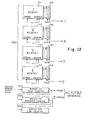
- FIG. 12 is a block diagram of a portion of the decoder memory subsystem, showing the output control and addressing threof.
- FIG. 13 is a block diagram of the pixel value generation circuitry of the decoder.
- FIG. 14 is a flow diagram for controlling the ROM sequencer of the decoder pixel value generation circuitry.
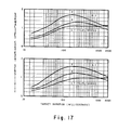
- FIG. 15 shows steady state contrast sensitivity curves of the eye.
- FIG. 16 shows relative sensitivity of the eye to luminosity gratings as a function of the duration of presentation of the grating.
- FIG. 17 shows curves for isoluminance chromaticity gratings as a function of duration.
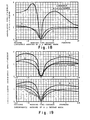
- FIG. 18 shows a plot of the relative response of the eye to masking.
- FIG. 19 illustrates relative response to masking for isoluminance chromaticity gratings.
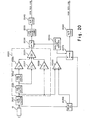
- FIG. 20 is a block diagram of the luminance processor portion of encoding circuitry in accordance with an embodiment of a further form of the invention.
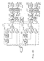
- FIG. 21 shows a block diagram of the chrominance processor portion of the encoding circuitry in accordance with an embodiment of the further form of the invention.
- FIG. 22 shows a block diagram of memory and output circuitry portions of an embodiment of the further form of the invention.
- FIG. 23 is a block diagram of decoding circuitry in accordance with the further form of the invention.
- Referring to FIG. 1, there is shown a block diagram of a high definition television system in accordance with a first embodiment of the invention. A high resolution television camera 10, which is assumed for ease of explanation to be a monochrome camera, generates television video signals which are coupled to encoding
circuitry 20. The encoding circuitry operates, in accordance with principles to be described, to digitize the video - frames into arrays of pixels and produce a sum or "intensity" signal I, and three difference signals designated at the X, Y and Z difference signals. The I signal contains information in a frequency bandwidth that is substantially equivalent to conventional television luminance bandwidth. The encoding circuitry also produces a plurality of auxiliary signals, called "difference signals", which, when taken in conjunction with the sum signal, can later be used to obtain substantially the high resolution information contained in the original digitized frames of video. The sum signal and the difference signals are converted to analog form and coupled to transmittingcircuitry 30 which may include means for modulating carriers with the sum and difference signals and transmitting the modulated characters. - At the receiver end, receiving
circuitry 40 recovers the sum and difference signals, which are in turn, coupled to decodingcircuitry 50. Thedecoding circuitry 50, digitizes the sum and difference signals and combines them to obtain a pixel value for each pixel of an output video frame that is equivalent to the 'pixel value of the corresponding pixel of the original high resolution frame digitized at the encoder. The high resolution digital video signal is converted to analog form and displayed on thedisplay 60. A feature of the invention is that the sum signal I is compatible with conventional'broadcast television and can be employed by home receivers which are not equipped with the decoder circuitry necessary to obtain the higher resolution video. - FIG. 2 is useful in understanding the manner in which the sum (or intensity) and difference signals can be generated for an array of pixels. In the FIGURE, the pixels are represented by the small dots, there being 1152 in a line, and 964 viewable lines per frame in the present example. The pixels of FIG. 2 can be thought of as "high resolution" pixels, in that there are approximately twice as many horizontal and vertical elements or pixels per frame as compared to conventional broadcast television. The pixels of the present embodiment are divided into groups of four pixels each, as shown. Therefore, the groups can be designated horizontally as
group 1 through group 576, and the lines of groups can be designated asgroup line 1 throughgroup line 482. Accordingly, the number of pixel groups approximately corresponds to the number of resolution elements in conventional broadcast television. In the present embodiment, a sum or intensity signal I is formed of the four pixels in each group, this sum signal (when properly scaled) being representative of the average intensity (or luminance) level in the elemental area defined by the pixel group. If the pixels in a given group n, falling on an adjacent line pair designated as line A and line B, are designated as A0n, A1n, B0n, and B1n, as illustrated in FIG. 2, then the sum or intensity signal, In, is expressed as:
- The difference signals of the present embodiment, expressed as Xn, Yn and Zn, and taken by subtracting the sum of the columns, the sum of the rows, and the sum of the diagonals, respectively, are as follows:


- The signs could, of course, be reversed for all difference signals. When the independent equations (1) through (4) are solved for A0n, B0n, A1n and Cln, the following solutions are obtained:


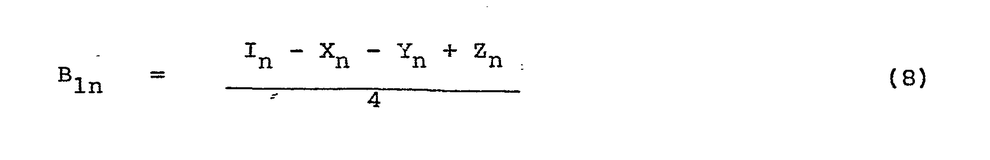
- Relationships (5) through (8) are used in the decoding circuitry at the receiver end to recover the pixel values originally stored at the encoder.
- In the present illustrative embodiment of the invention, the "low resolution" intensity signal I (which will be understood hereinafter to be at substantially conventional broadcast television resolution) is generated at the conventional television video frame rate, and a full complement of difference signals is generated at one-third the conventional television video frame rate. It will be understood, however, that various rates can be employed, as described further hereinbelow. In the present embodiment the difference signals X, Y and Z are formed in sequence, one frame of a single difference signal being formed during the period of a conventional television video frame.
- Referring to FIG. 3, there is shown a simplified block diagram of the
encoding circuitry 20 of the first embodiment. The video signal from camera 10 (FIG. 1) is coupled to an analog-to-digital converter 210 which conventionally operates to convert the television signal to digital form. In the present embodiment, each video pixel of a frame is represented by an 8- bit binary signal that is determined by the instantaneous luminance level of the video signal at the particular pixel position. The analog-to-digital converter 210 operates to digitize each pixel at the encoder input clock rate, and couple the 8-bit pixel values to theencoder memory subsystem 300. Reference can also be made to FIG.s 4 and 5 for further detail. In particular, the output of analog-to-digital converter 210 is coupled to the input of a 24-stage serial-in-parallel-outbuffer register 310, which is also clocked at the encoder input clock rate. Thebuffer register 310 is operative to receive twenty- four 8-bit pixel values from the analog-to-digital converter and, when full, the buffer register contents are strobed into the input port of therandom access memory 320. In the present embodiment thememory 320 stores one frame of 8-bit pixels of the high resolution video. Thememory 320 has a pair of output ports respectively designated as an A port and a B port. The A port is used to output the pixel values of an odd-numbered line, and the B port is used to output the pixel values of the adjacent even- numbered line. In this manner, the pixels of the groups of FIG. 2 are conveniently accessed to produce the desired sum and difference signals. To facilitate fast processing, and as will -be described further hereinbelow, the sum and difference signals are formed using sum and difference signal generationdigital circuitry 600 that simultaneously processes pixel values from the A and B ports. [An independent pair of ports, designated as an A' port and a B' port can be used for difference signal formation, as will be described hereinbelow.] The output ofcircuitry 600 is coupled to digital-to-analog converters 301, which convert the sum and difference signals to analog signals that are coupled to the transmit circuitry 30 (FIG. 1). - FIG. 4 illustrates the input control and addressing of the
encoder memory subsystem 300. As previously described, pixels are clocked into thebuffer register 310 at the encoder input clock rate. A modulo 24pixel counter 330 is provided to count clock pulses and generate an output when theinput buffer register 310 is loaded with the latest 24 8-bit pixel values. The output ofcounter 330 is applied to strobe the 24 pixel values into thememory 320 via its input port. The output ofcounter 330 is also coupled to a modulo 48counter 340 that keeps track of the number of 24-pixel sequences that have been read in per line. Accordingly, the count ofsequence counter 340 is a "sequence address"; i.e., a number from 0 to 47 that designates a portion of the address where the latest 24-pixel sequence is to be stored in the memory. The output ofsequence counter 340 is also coupled to a modulo 964 line counter that is, accordingly, stepped at the end of each line and which theeby generates the portion of the address which designates the line of pixels being read in. In this manner, it will be understood that a composite address is generated for each sequence of 24 high resolution pixels, so that a full frame of high resolution pixels can be stored at readily retrievable locations of the memory 320. - FIG. 5 illustrates the output control and addressing of the encoder memory subsystem. As noted above, the memory has output ports, designated as port A and port B. When the port A output is operating to read out pixel values of a particular scanline, the port B is used to read out pixel values of the corresponding pixels of the next scanline. This facilitates the generation of the sum and difference signals. Output from each port, in parallel, are twelve consecutive pixel values of a scanline; i.e., one-half of a 24-pixel sequence as described in conjunction with the encoder memory input addressing and control. A port A
output buffer register 360 and a port Boutput buffer register 365 are each 12-stage parallel-in-serial-out registers which operate under control of the encoder output clock. - A modulo 12
counter 370 counts encoder output clock pulses, and thereby generates an output that is used to strobe a sequence of 12 pixels of each of two consecutive scanlines into the parallel-in-serial-out output buffer registers 360 and 365 for port A and port B, respectively. The output ofcounter 370 is coupled to amodulo 2sub-sequence counter 375 that keeps track of which half of the originally stored 24 pixel sequence is being addressed. Accordingly, the single bit output ofcounter 375 is a part of the address input to encoder memory output ports. Thecounter 375 output is coupled to a modulo 48sequence counter 380, whose output count is another portion of the address; i.e., 'the designation of the particular 24-pixel sequence being addressed at both ports. The output ofcounter 380 is coupled to a modulo 241line counter 385 whose output is coupled to a multiply-by-fourcircuit 386. The output ofmultiplier 386 is coupled to one input ofadder 387. The other input to adder 387 is the output ofgate 388. Thegate 388 has an input representative of thenumber 2, and is enabled during generation of an odd television field. The output ofadder 387 is the line number portion of the port A address, and it is also coupled to anotheradder 389 which adds 1. The output ofaddder 389 is the line number portion of the port B address. In operation, the line addressing circuitry just described operates such that the port A line addresses designate the odd lines and the port B addresses designate the even lines. During an even field, the line pairs 0,1 then 4,5 then 8;9... are addressed, and during the odd field thelines - FIG. 6 illustrates the portion of the sum and difference
signal generation circuitry 600 used for generating the intensity signal I from the port A and port B outputs as they are clocked serially out of the buffer registers 360 and 365, respectively. The circuitry includesarithmetic logic units storage registers arithmetic logic unit 610 receives the port A and port B outputs. The output ofarithmetic logic unit 610 is coupled tostorage registers 615 and 620 whose outputs are, in turn, coupled to thearithmetic logic unit 625. The output ofarithmetic logic unit 625 is, in turn, coupled tostorage register 630, whose output is the desired sum signal, I, in accordance with the relationship (1) above. - The described arithmetic logic units and storage registers are under control of
ROM sequencer 605 which receives the vertical and horizontal synchronizing signals and the encoder output clock signal and generates the control sequence illustrated by the flow diagram of FIG. 7 to obtain the sum set forth in relationships (1). In particular, the first pixel pair from port A and port B is input to thearithmetic logic unit 610, as represented by theblock 721. Thearithmetic logic unit 610 is controlled to form the sum of this first pixel pair; i.e., to form (AO + B ) as illustrated in the group of FIG. 2, and as represented by theblock 722. The output ofarithmetic logic unit 610 is stored in register 615 (block 723). The second pixel pair of the group is then input to arithmetic logic unit 610 (block 724) which is again controlled to form an addition function (block 725). The result is stored in register 621 (block 725). The outputs ofregisters arithmetic logic unit 625 is stored in register 630 (block 729) and output from register 630 (block 730) to serve as the sum signal output I that is coupled to transmit circuitry 30 '(e.g. FIG. 1). - FIG.--8 illustrates the portion of the sum and difference signal generation circuitry 600 (FIG. 3) used for generating the difference signals X, Y and Z from the port A and port B outputs as they are clocked serially out of the buffer registers 360 and 365, respectively. The circuitry includes
arithmetic logic units storage registers arithmetic logic unit 660 receives the port A and port B pixel streams. The output ofarithmetic logic unit 660 is coupled tostorage registers arithmetic logic unit 675. The output ofarithmetic logic unit 675 is, in turn, coupled tostorage register 680, whose output is, depending upon time, either the X, Y, or Z difference signal in accordance with relationships (2), (3) or (4) above. The described arithmetic logic units and storage registers are under control ofROM sequencer 655, which receives the vertical and horizontal synchronizing signals and the encoder output clock signal, and generates the control sequence illustrated by the flow diagram of FIG. 9 to obtain the desired difference signals. A modulo 3counter 690 is responsive to alternate vertical synchronizing signals to produce one of three output counts that serve as the code to determine which of the X, Y or Z difference signals is to be generated for a particular frame. This output code is also coupled to the transmitcircuitry 30 so that it can be transmitted and used in the decoder circuitry of the receiver in order to distinguish between the difference signals at the decoder. - In FIG. 9,
decision diamond 905 represents determination of which difference signal code, X, Y or Z, is active. If the X code is active, theblock 911 is entered, this block representing the inputting of the first pixel pair from port A and port B to thearithmetic logic unit 660. Thearithmetic logic unit 660 is controlled to form the sum of this pixel pair, as represented by theblock 912. The output ofarithmetic logic unit 660 is stored in register 665 (block 913). The second pixel pair of the group is then input to arithmetic logic unit 660 (block 914), which is again controlled to form an addition function (block 915). The result is stored in register 670 (block 916). The output ofregisters arithmetic logic unit 675 is stored in register 680 (block 921), and output from register 680 (block 922) as the difference signal X that is coupled totransmitter circuitry 30. The process is then repeated for the two pixel pairs of the next group, and the procedure is continued for each scanline pair of the frame. In this manner, it is seen that the X difference signal is formed in accordance with the relationship (2) above. - During the next frame, when the Y code is active, the branch beginning with
block 931 is operative. In particular, the first pixel pair is input to the arithmetic logic unit 660 (block 931) which is controlled to form the difference of this pixel pair, i.e. (AO - BO) as represented byblock 932. The output ofarithmetic logic unit 660 is stored in register 665 (block 934). The second pixel pair of the group is then input to arithmetic logic unit 660 (block 934) which is again controlled to perform a subtraction (block 935). The result is stored in register 670 (block 936). The output ofregisters arithmetic logic unit 675 which is controlled to form a sum (block 938).Blocks register 680 and the output fromregister 680 of the Y difference signal, consistent with the relationship set forth above in equation (3). - During the next frame, when the Z code is active, the branch beginning with
block 941 is operative. The first pixel pair is input to the arithmetic logic unit 660 (block 941) which is controlled to form the difference of this pixel pair, i.e. (A0 - B0) as represented byblock 942. The output ofarithmetic logic unit 660 is stored in register 665 (block 943). The second pixel pair of the group is then input to arithmetic logic unit 660 (block 944) which is again controlled to perform a subtraction (block 945). The result is stored in register 670 (block 946). The output ofregisters arithmetic logic unit 675 which is controlled to perform a subtraction (block 948).Blocks register 680 and the output fromregister 680 of the Z difference signal, consistent with the relationship set forth above in equation (4). - Referring to FIG. 10, there is shown a simplified block diagram of the decoding circuitry 50 (FIG. 1). The sum and difference signals,recovered by receiver circuity 40 (FIG. 1) are coupled to analog-to-
digital converters 1010 which operate to convert the sum and difference signals to digital form. The digitized signals are coupled to the decoder memory subsystem 1100 which is operative in the present embodiment to produce simultaneously, at four output ports, the latest digital information representative of the sum signal (I) and the three difference signals (X, Y and Z). These signals are combined by pixelvalue generation circuitry 1300, in accordance with the relationships (5), (6), (7) and (8), to recover the high resolution pixel values originally stored at the encoder. The output ofcircuitry 1300 is coupled to digital-to-analog converter 1015 which converts the digital signal output fromcircuitry 1300 into analog form suitable for display onhigh resolution monitor 1018. - FIG. 11 illustrates the input control and addressing of the
decoder memory subsystem 1100. The memory portion thereof is organized in the present embodiment as four two-port memory blocks of random access memory, each capable of storing 576 (12 x 48) 8-bit pixel values per line, by 482 lines. The four portions of the decoder memory are called theintensity memory 1121, the X difference-signal.memory 1122, Ydifference signal memory 1123, and the Zdifference signal memory 1124. These portions of the memory are operative to respectively store, via their input ports, the signals designated I, X, Y and Z, these signals then being read out at the respective output ports of the memory portions and combined in a manner to be described. - The intensity channel signal I is received by analog-to-digital converter 1010a which converts the analog signal to 8-bit digital pixel values at a decoder intensity channel clock rate that is typically the same as the encoder output clock rate. An
input buffer register 1130 is a serial-in-parallel-out register that receives twelve 8-bit pixel values which are strobed in parallel into thememory 1121. A modulo 12counter 1135 counts the clock pulses and produces a strobe signal that is operative to strobe twelve pixels of information from thebuffer 1130 into thememory 1121. The output of modulo 12counter 1135 is counted by a modulo 48counter 1140, the count of which comprises the sequence address portion of the address coupled tomemory 1121. The output of modulo 48counter 1140 is coupled to a modulo 482counter 1141 whose count constitutes the line address input tomemory 1121. Accordingly, each group of twelve 8-bit pixels is strobed into an appropriate sequence address and line address in thedecoder intensity memory 1121. - The difference channel signal is coupled to an analog-to-digital converter 1010b which converts the difference channel signal to 8-bit pixel values at a decoder difference channel clock rate that may be the same or different than the decoder intensity channel clock rate. The difference channel signal is also coupled to a
decoder 1155 which detects the difference process code (X, Y or Z), as previously described, to determine which of the X, Y or Z difference signals is active during the present frame. The output ofdecoder 1155 couples an enabling signal to one of three gates; i.e., anX gate 1156, aY gate 1157 of aZ gate 1158, depending upon which difference signal is active. The decoded signal is also coupled to the X, Y and Z memories as an address select indication. The 8-bit pixel value output from the analog-to-digital converter 1010b is coupled through theenabled gate buffer register - The input address generation for the X, Y, and Z portions of the
decoder memory intensity memory section 1121. (If the input clocks are selected as being the same, the input address generation for the X, Y and Z memory sections may be in common with the input address generation for the intensity memory section.) The clock signal is coupled to a modulo 12counter 1181 whose output is the strobe signal used to strobe the contents ofbuffers counter 1181 is coupled to a modulo 48'counter 1182 whose count constitutes the sequence address for the sequence of twelve pixels being strobed in, as described above. Also, the output of the modulo 48counter 1182 is coupled to a modulo 482 counter 1183 whose output, again, serves as a line address. The strobe and address signals are coupled to each of thememories decoder memory section 1121 and sequentially stores frames of the X difference signal, the Y difference signal and the Z difference signal in thememory sections - Referring to FIG. 12, there is shown the receiver memory output ports and output addressing. The
memory portions - A modulo 24
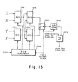
counter 1231 counts decoder memory output clock pulses, which are at a higher rate (for example, twice the rate in this embodiment) than the decoder memory input clocks. The output of the modulo 24counter 1231 is used as a strobe signal to strobe the 24 pixels in parallel from thememories output buffer registers counter 1231 is also coupled to the input of the modulo 24counter 1232 whose count is utilized as the sequence address to the fourmemories counter 1232 is coupled to a modulo 482 counter 1233 whose count is utilized as a line address to thememories memories - Referring to FIG. 13, there is shown a block diagram of the pixel value generation circuitry 1300 (FIG. 10) of the decoder which operates on the outputs of the decoder memory subsystem to reproduce the original pixel values in accordance with relationships (1) through (4) above. Four
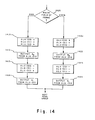
arithmetic logic units 1310, 1311, 1312 and 1313 are employed, under control ofROM sequencer 1305. Thearithmetic logic unit 1310 receives the sum signal I and one of the difference signals X, and thearithmetic logic unit 1311 receives the difference signals Y and Z. The output ofarithmetic logic unit 1310 is coupled to an input of each of thearithmetic logic units arithmetic logic unit 1311 is coupled to the other input of each of thearithmetic logic units arithmetic logic units solid state switch 1320, the output ofswitch 1320 being coupled to the input of digital-to-analog converter 1350. The output ofconverter 1350 is coupled to a summingcircuit 1375 which also receives locally generated composite sync and blanking (which, as previously noted, is synchronized with the received television signal) to produce a composite output high definition television signal. Theswitch 1320 and the digital-to-analog converter 1350 operate at the decoder video output clock rate which is typically the same clock rate as the encoder input clock rate that was used to originally clock in the high resolution pixel information.ROM sequencer 1305, which receives sync and the video output clock, controls the status of the arithmetic logic units. - FIG. 14 illustrates the routine of the
ROM sequencer 1305.Decision diamond 1405 represents an inquiry as to which field of a frame is being generated, the field information being available to the ROM sequencer from the sync and blanking circuitry of the receiver. If it is the first field of the frame (an odd field), and odd output lines are to be generated, it will be understood that pixels A0 and A1 of each pixel group are to be generated (see FIG. 2). Pixel A0 is generated in accordance with relationships (5). Theblock 1411 represents the control of thearithmetic logic units arithmetic logic unit 1312 represents A0 in accordance with relationship (5) (block 1412). Thesolid state switch 1320, which is clocked at the same rate as the ROM sequencer by the decoder video output clock, is synchronized to sample the output of thearithmetic logic unit 1312 for pixel A of each group and to sample the output of thearithmetic logic unit 1313 for pixel Al of each group. To process the next pixel, upon occurrence of the next clock pulse, thearithmetic logic units arithmetic logic unit 1313 is controlled to perform an addition (block 1413), so that the output of the arithmetic logic unit (block 1414) is consistent with the desired expression for A in accordance with relationship (6). This signal is output fromarithmetic logic unit 1313 as thesolid state switch 1320 samples the output ofarithmetic logic unit 1313. The adjacent pixel pairs of each odd line continue to be processed in this way. When the second (even) field of the frame is being generated, the outputs ofarithmetic logic units solid state switch 1320, are used to generate signals for B0 and B1 respectively, consistent with relationships (7) and (8). - In particular, for the pixel B0, the
arithmetic logic units arithmetic logic unit 1312 is controlled to perform a subtraction (block 1421), so that the output BO pixel from arithmetic logic unit 1312 (block 1422) is in accordance with the expression (7). As described above, this pixel value is output to thesolid state switch 1320 in synchronism with the switch sampling the output fromarithmetic logic unit 1312. When the solid state switch is receiving the output ofarithmetic logic unit 1313, thearithmetic logic units - In the described exemplary embodiment, the encoder generates a full complement of difference signals at one-third the rate at which the low resolution intensity (sum) signal is generated. Since different individual ones of the difference signals are generated concurrently with the intensity signal, the signals from the output ports A and B (FIG. 5) can be utilized to generate both the sum and the difference signals (using the combining circuitry of FIG.s 6 and 8). However, it may be preferable to save additional bandwidth by further slowing down the rate of generation of the difference signals to the full extent allowed by visual perception considerations, as described further hereinbelow. In FIG. 5, the ports designated A' and B', and their associated clocks, allow independent generation of the difference signals at any desired rate.
- Also, in the described first embodiment hereof, the decoder is implemented using memories which store the incoming intensity (sum) and difference signals, and then read out the stored signals (redundantly, at least in the case of the difference signals) to combining circuitry which generates the high resolution pixel values. It is important to note, however, that the decoder could alternatively be implemented by combining previously stored high resolution pixel values (i.e., from a previous frame) with the sum and difference signals as they are received.
- The exemplary first embodiment hereof has been described in terms of a monochrome system, but principles of the invention apply to color systems, as well, as disclosed further hereinbelow. For a broadcast television application, color can be encoded on the 525 line carrier in the usual way. For high definition reception a higher resolution chroma signal is used. For example, quadrature chroma coordinates can be transmitted at 525 line resolution both horizontally and vertically. The information need not be generated (or transmitted) at 30 frames per second, lower chromaticity frame rates being preferred to save bandwidth, as will be further described. Difference signals containing the high resolution chromaticity information can be employed and sent frame sequentially.
- As noted above, various pixel group configurations, which may be square, rectangular, linear, or irregular, can be used, consistent with the principles of the present invention. The number of difference signals necessary in each case will be a function of the number of pixels in a group.
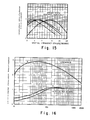
- Before describing a further embodiment of the invention, psychophysical measurements conducted by applicant, and upon which certain aspects of the invention are based, will be reviewed. The threshold of contrast sensitivity for monochrome luminance gratings and isoluminance chromaticity gratings were measured at a number of temporal frequencies over the spatial frequency range of importance in television at normal viewing distances. This provided a series of modulation transfer functions of the eye at these spatial and temporal frequencies. The measurements provide some,of the information required in determining the time constants of the eye to both luminance and chrominance - and also can be used in re-evaluation of the desired proportions in resolution required for luminance and the primary color difference signals.
- An abridged version of the steady state contrast sensitivity curves of the eye is shown in FIG. 15. This figure shows response of the eye for luminance and for isoluminance complementary color pairs on lines on the CIE diagram which go through luminance C white and the three NTSC primary colors. The color curves have been normalized so that the peak sensitivity of all four curves is equal. This normalization makes the minimum perceptible color difference equal in contrast to the minimum perceptible luminance contrast for all three primaries at low spatial frequencies. The curves are terminated at the spatial frequency at which color is no longer perceived. Gratings above this spatial frequency are still visible but appear to be monochrome at all color contrasts. From these curves and termination points, it is evident that the color difference signals should be about half the luminance bandwidth for R-Y and one-quarter that bandwidth for B-Y.
- A second series of measurements were made to determine the perception of spatial frequencies as a function of duration. Durations were used that were 1, 2, 4, 8, 16, 32, 64 and 128 fields (17 milliseconds per field.) FIG. 16 shows the relative sensitivity of the eye to luminosity gratings as a function of the duration of presentation of the grating. This is shown at .6, 4 and 12 cycles per degree. At low spatial frequencies in both luminance and chrominance, the eye adapts in time to the grating, making it appear less visible. For short duration presentations at about .1 second, these spatial frequencies are greatly enhanced in visibility compared with the steady state visibility of the grating. For very short presentations, all spatial frequencies are suppressed. FIG. 17 shows the corresponding curves for isoluminance chromaticity gratings as a function of duration at .2, .9 and 2.7 cycles per degree.
- In the presence of motion there is generally a low spatial frequency brightness change which suppresses reception for a period of time. The suppression of the grating (target) actually precedes the mask for a short time. The target was presented before the mask (backward masking) as well as after the mask (forward masking). The degree of suppression by a .1 second mask was measured using off-the-air television as signal during the mask. The spatial frequencies (target grating) were presented for various intervals either immediately preceding or immediately succeeding the mask.
- FIG. 18 shows a plot of the relative response of the eye to these stimuli as the grating duration was changed either immediately preceding or succeeding the mask. This experiment combines the effects of duration (FIG.s 16 and 17) and masking. It represents what would happen to the sensitivity of the eye in detail information in the scene that was just uncovered by a moving object in the image.
- FIG. 19 shows the corresponding curve to FIG. 18 for isoluminance chromaticity gratings. As one can see, the suppression is significant in excess of 200 millisecond period above 4 cycles per degree in luminance and above .9 cycle per degree in chrominance. The masking is primarily forward masking for both luminance and chrominance. The suppression of low Spatial frequency luminance information in the target occurs only for about 50 milliseconds before or after the mask. From this one would conclude that a frame rate of about 20 frames per second is necessary to depict motion at low spatial frequencies, as is known in motion picture technology.
- In a further form of the invention, electronic processing is performed to obtain low and high spatial frequency Component representations of an image before storage of frames in digital form. The low spatial frequency representations can be used for the compatible standard resolution transmission.
- Referring to FIG. 20, there is shown a block diagram of the luminance processor portion of an encoding circuitry (20) embodiment in accordance with the further form of the invention. The high resolution video signal from
camera 10 is coupled to a low pass filter 2010 whose output, which is used to obtain the standard resolution video, is coupled to 3-linevertical Gaussian averager 2020. Thecircuit 2020 includes two series one line delays 2021 and 2022,weighting amplifiers amplifier 2029. Corresponding vertical elements of three successive scanlines are coupled to theweighting amplifiers summer 2029. Applicant found that a spatial frequency aliasing artifact can occur on a standard resolution receiver if alternate high resolution lines are used to generate the standard resolution signal, due to the rectangular pulse nature of the sampling window used. By summing proportionally weighted values of elements from at least three successive lines, the artifact can be substantially eliminated. - The output of
circuit 2020 is coupled to solidstate switching circuit 2030, which is responsive to an odd/even line indicator 2040 to pass an output signal only during occurrence of odd lines of the high resolution video signal. Before coupling of the output of switchingcircuit 2030 to an analog-to-digital converter 2045, an optional timebase corrector circuit 2035 can be used (since there is an output only every other line) to reduce the sampling speed requirements of the analog-to-digital 'converter 2045 and the size of the memory in which the standard resolution luminance is to be stored. - In order to ultimately reconstruct the high resolution image luminance, the even line signals, as well as the high frequency components of the odd line signals, are used to obtain a high band luminance signal. In the illustrated embodiment, the high resolution video from
camera 10 is also coupled to adelay equalizer 2050, an output of which is coupled to the positive input terminal of adifference amplifier 2060. Thedifference amplifier 2060 subtracts low band components from high band components of the odd line signals, the selection of odd lines from the difference amplifier output being achieved by anotherswitching circuit 2070 under control of odd/evenline indicator 2040. The other input to switchingcircuit 2070 is the high band even line luminance signal. Accordingly, the output of switchingcircuit 2070, which is coupled to analog-to-digital converter 2080, contains the luminance components of the high resolution video signal, except for the low resolution components associated 'with the odd lines, which are used in generating the standard resolution signal (to avoid redundancy of this information, and save bandwidth, as in the previous embodiment). - The present embodiment illustrates the handling of color, and FIG. 21 shows a block diagram of the chrominance processor portion of the encoding circuitry. In this embodiment, color difference signals designated B-Y and R-Y are illustrated as being output from
high resolution camera 10, although these can be selected at particular orthogonal reference positions of a color vectorscope that do not necessarily correspond to B-Y and R-Y. The chrominance processing of this embodiment has a number of aspects that are similar to the luminance processing described in conjunction with FIG. 20. Vertical spatial filtering is again provided by using two 1-line delays for each of the color component signals. In this case, however, standard NTSC chrominance vertical spatial frequency characteristics are adequate for high resolution color, so only the odd-line information is processed to obtain both the standard resolution color component signals and the high resolution color component signals. The R-Y and B-Y signals are respectively coupled tocircuits Gaussian averaging circuit 2020 of FIG. 20. In particular, each of these circuits includes a pair of 1-line delay circuits weighting amplifiers amplifier 2119. The outputs of thecircuits circuits line indicator 2040 to pass an output signal only during occurrence of the odd lines of the high resolution video signal. The output of switchingcircuit 2115 is coupled to alow pass filter 2130 and is also coupled, viadelay equalizer 2131, to the positive input of adifference amplifier 2132. The negative input of thedifference amplifier 2132 receives the output oflow pass filter 2130. The outputs oflow pass filter 2130 anddifference amplifier 2132 are respectively coupled to optional timebase corrector circuits base corrector circuits digital converters - In the B-Y channel, the output of switching
circuit 2125 is coupled to circuits having substantially the same functions as those set forth with respect to the R-Y channel. However, prime designations are used in indicating the reference numerals of the circuits. In this channel, the low pass filter 2130' and analog-to-digital converter 2144' can operate at lower frequency (e.g. half the frequency and half the line rate) than their counterparts in the R-Y channel. This is because of the lower bandwidth requirement of the standard resolution B-Y signal. - Referring to FIG. 22, there is shown a block diagram of memory and output embodiments of the encoding circuitry (20) of the further form of the invention. The six outputs of the FIG. 21 circuitry (standard resolution luminance, R-Y, and B-Y, and high resolution luminance, R-Y and B-Y) are coupled to six memories 2211-2216, the memories being provided with independent input and output port capabilities, as described, for example, in conjunction with above first embodiment, to allow for adjustability of the input and/or output rate of the digital information stored in the memories. In an example of the present embodiment, the inputs to the memories are at the nominal rate of 30 frames per second, and the outputs of the memories holding the standard resolution signals are also at 30 frames per second (although it will be understood, throughout, that other rates can be used). The high resolution luminance output of
memory 2214 has an output frame rate preferably between 3 and 15 frames per second. A rate of about 5 frames per second is considered to be suitable for maximizing the bandwidth saving while substantially maintaining high resolution integrity. In the present embodiment the high resolution R-Y frame rate is the same as the high resolution luminance frame rate, and the high resolution B-Y frame rate is preferably in the range between 3 and 30 frames per second (and can be at the nominal 30 frame per second rate without significant compromise of bandwidth, since the B-Y signal can be transmitted with only one-quarter the R-Y bandwidth, consistent with NTSC standard television). - The outputs of the memories 2211-2216 are coupled to digital-to-analog converters 2221-2217, respectively. The standard resolution color difference signals can be quadrature modulated onto a color subcarrier signal (block 2230) and the resultant chrominance signal can be combined with the luminance signal, using
summer 2240, to obtain a color video signal at substantially standard resolution. The video signal is delayed bydelay circuit 2250 and then transmitted and/or recorded. The high resolution signals can also be transmitted and/or recorded, such as by transmit circuitry 30 (FIG. 1). The purpose of the delay (which may alternatively be individual delays in the separate channels) is to maximize the masking of the slow buildup of the high resolution information in the ultimately displayed image, as described above, by effectively accelerating the high resolution portions of the image with respect to low resolution portions thereof. The delay is preferably in the range of 30 to '200 milliseconds. If the delay is too long, detail will appear before it is supposed to be visible. - Referring to FIG. 23, there is shown a block diagram of an embodiment of a decoder in accordance with the further form of the invention. It will be understood that the standard resolution video signal can be utilized by a standard resolution receiver (e.g. as illustrated in FIG. 1) after reception by receiver circuitry (40). In the high resolution decoder of FIG. 23, the standard resolution channel is coupled to a
low pass filter 2305 which removes the chrominance, and also to aquadrature detector 2306 which operates in conjunction withlow pass filters digital converters digital converters circuit 2340 to "unaverage" in a vertical direction. An odd line from standardresolution luminance memory 2321, and adjacent even lines from highresolution luminance memory 2324 are coupled through respective digital-to-analog converters weighting amplifiers summer 2344 whose output is, in turn, low pass filtered byfilter 2345. The odd line output from highresolution luminance memory 2324 is coupled to digital-to-analog converter 2334, whose output is high pass filtered byfilter 2346, and then coupled to one input ofsummer :2347, the other input to which is the output oflow pass filter 2345. Accordingly, the output ofsummer 2347 is the recovered high resolution odd line information. [It will be understood that odd and even lines can be obtained using appropriate line delays with respect to the memory outputs, or by providing appropriate output port access for the different line information.] - The output of digital-to-
analog converter 2333, which is high resolution even line information, is one input tosolid state switch 2350, the other input to which is the high resolution odd line information output ofsummer 2347. Theswitch 2350 is under control of an odd/even line indicator 2351 to select either the high resolution odd line information or the high resolution even line information, depending upon the current line status. - The high resolution color difference signals are recovered in a similar manner. In this case, the low and high resolution R-Y signals from
memories analog converters filters filters summer 2358 whose output will therefore constitute the odd line R-Y signal (remembering that the color difference signals were obtained only from the odd lines). The output ofsummer 2358 is coupled to a oneline delay 2361 whose output is one input to anothersummer 2362. The other input tosummer 2362 is the output ofsummer 2358. Thesummer 2362 has an inherent weighting factor of 1/2, so that its output is an average of successive odd lines. Asolid state switch 2363 is then used to alternate between the odd line output ofsummer 2358, and the even line output ofsummer 2362 that is derived from averaging odd lines. The output of the solid state switch contains the high resolution R-Y signal. - The high resolution B-Y signal is recovered in the same manner as the R-Y signal. In particular, the outputs of high resolution and standard resolution B-Y memories are coupled to digital-to-
analog converters filters high resolution display 60. - It will be recognized by those skilled in the art that further variations can be implemented within the spirit and scope of the invention. For example, if required by broadcast standards a "high resolution signal killer" could be utilized in high definition receivers when low resolution broadcasts are being received. Also, while a double interlace scheme has been illustrated, it will be understood that alternatives, such as triple interlace, can be used. Further, and as referred to above, the standard frame rate can be other than the 30 frames per second NTSC rate used in the U.S., and the invention has applicability to any type of video system. Finally, it is noted that integrated circuit technology can be employed to implement some or all of the encoder or the decoder, such as for home receiver use.
Claims (23)
Applications Claiming Priority (6)
| Application Number | Priority Date | Filing Date | Title |
|---|---|---|---|
| US41805382A | 1982-09-14 | 1982-09-14 | |
| US418053 | 1982-09-14 | ||
| US06/418,055 US4517597A (en) | 1982-09-14 | 1982-09-14 | Method and apparatus for encoding and decoding video |
| US06/483,126 US4628344A (en) | 1982-09-14 | 1983-04-08 | Method and apparatus for encoding and decoding video |
| US483126 | 1983-04-08 | ||
| US418055 | 2006-05-05 |
Publications (3)
| Publication Number | Publication Date |
|---|---|
| EP0103488A2 true EP0103488A2 (en) | 1984-03-21 |
| EP0103488A3 EP0103488A3 (en) | 1986-06-25 |
| EP0103488B1 EP0103488B1 (en) | 1991-03-27 |
Family
ID=27411167
Family Applications (1)
| Application Number | Title | Priority Date | Filing Date |
|---|---|---|---|
| EP83305384A Expired - Lifetime EP0103488B1 (en) | 1982-09-14 | 1983-09-14 | Method and apparatus for encoding and decoding video |
Country Status (2)
| Country | Link |
|---|---|
| EP (1) | EP0103488B1 (en) |
| DE (1) | DE3382229D1 (en) |
Cited By (9)
| Publication number | Priority date | Publication date | Assignee | Title |
|---|---|---|---|---|
| FR2539570A1 (en) * | 1983-01-19 | 1984-07-20 | Rca Corp | COMPATIBLE HIGH-DEFINITION TELEVISION SYSTEM USING THE BASIC FUNCTIONS OF HADAMARD |
| EP0178938A2 (en) * | 1984-10-17 | 1986-04-23 | New York Institute Of Technology | Television apparatus and method |
| EP0284427A2 (en) * | 1987-03-26 | 1988-09-28 | New York Institute Of Technology | Method and apparatus for video signal processing |
| US4794457A (en) * | 1986-10-31 | 1988-12-27 | Thomson-Csf | Video signal mixer circuit for high-resolution imaging with solid-state matrix sensor cameras |
| WO1990005430A1 (en) * | 1988-11-11 | 1990-05-17 | General Electric Company | Quadruplex encoding for actv |
| DE10349437B3 (en) * | 2003-10-21 | 2005-02-10 | Werkzeugmaschinenbau Sinsheim Gmbh | Central drive rotary machine tool for machining workpieces has a machine bed arranged vertically with transverse carriage on upper guide track |
| WO2013086169A1 (en) * | 2011-12-06 | 2013-06-13 | Dolby Laboratories Licensing Corporation | Device and method of improving the perceptual luminance nonlinearity - based image data exchange across different display capabilities |
| US9202438B2 (en) | 2011-09-26 | 2015-12-01 | Dolby Laboratories Licensing Corporation | Image formats and related methods and apparatuses |
| US10242650B2 (en) | 2011-12-06 | 2019-03-26 | Dolby Laboratories Licensing Corporation | Perceptual luminance nonlinearity-based image data exchange across different display capabilities |
Citations (1)
| Publication number | Priority date | Publication date | Assignee | Title |
|---|---|---|---|---|
| US2686831A (en) * | 1950-10-31 | 1954-08-17 | Gen Electric | High-definition television system and method |
-
1983
- 1983-09-14 DE DE8383305384T patent/DE3382229D1/en not_active Expired - Lifetime
- 1983-09-14 EP EP83305384A patent/EP0103488B1/en not_active Expired - Lifetime
Patent Citations (1)
| Publication number | Priority date | Publication date | Assignee | Title |
|---|---|---|---|---|
| US2686831A (en) * | 1950-10-31 | 1954-08-17 | Gen Electric | High-definition television system and method |
Cited By (27)
| Publication number | Priority date | Publication date | Assignee | Title |
|---|---|---|---|---|
| FR2539570A1 (en) * | 1983-01-19 | 1984-07-20 | Rca Corp | COMPATIBLE HIGH-DEFINITION TELEVISION SYSTEM USING THE BASIC FUNCTIONS OF HADAMARD |
| EP0178938A2 (en) * | 1984-10-17 | 1986-04-23 | New York Institute Of Technology | Television apparatus and method |
| EP0178938A3 (en) * | 1984-10-17 | 1986-07-16 | New York Institute Of Technology | Television apparatus and method |
| US4794457A (en) * | 1986-10-31 | 1988-12-27 | Thomson-Csf | Video signal mixer circuit for high-resolution imaging with solid-state matrix sensor cameras |
| EP0284427A2 (en) * | 1987-03-26 | 1988-09-28 | New York Institute Of Technology | Method and apparatus for video signal processing |
| EP0284427A3 (en) * | 1987-03-26 | 1989-08-23 | New York Institute Of Technology | Method and apparatus for video signal processing |
| WO1990005430A1 (en) * | 1988-11-11 | 1990-05-17 | General Electric Company | Quadruplex encoding for actv |
| DE10349437B3 (en) * | 2003-10-21 | 2005-02-10 | Werkzeugmaschinenbau Sinsheim Gmbh | Central drive rotary machine tool for machining workpieces has a machine bed arranged vertically with transverse carriage on upper guide track |
| US9685120B2 (en) | 2011-09-26 | 2017-06-20 | Dolby Laboratories Licensing Corporation | Image formats and related methods and apparatuses |
| US9420196B2 (en) | 2011-09-26 | 2016-08-16 | Dolby Laboratories Licensing Corporation | Image formats and related methods and apparatuses |
| US9202438B2 (en) | 2011-09-26 | 2015-12-01 | Dolby Laboratories Licensing Corporation | Image formats and related methods and apparatuses |
| AU2016203100B2 (en) * | 2011-12-06 | 2016-08-04 | Dolby Laboratories Licensing Corporation | Device and Method of Improving the Perceptual Luminance Nonlinearity-Based Image Data Exchange Across Different Display Capabilities |
| AU2016203103B2 (en) * | 2011-12-06 | 2018-04-19 | Dolby Laboratories Licensing Corporation | Device and Method of Improving the Perceptual Luminance Nonlinearity-Based Image Data Exchange Across Different Display Capabilities |
| US9077994B2 (en) | 2011-12-06 | 2015-07-07 | Dolby Laboratories Licensing Corporation | Device and method of improving the perceptual luminance nonlinearity-based image data exchange across different display capabilities |
| US9521419B2 (en) | 2011-12-06 | 2016-12-13 | Dolby Laboratories Licensing Corproation | Perceptual luminance nonlinearity-based image data exchange across different display capabilities |
| WO2013086169A1 (en) * | 2011-12-06 | 2013-06-13 | Dolby Laboratories Licensing Corporation | Device and method of improving the perceptual luminance nonlinearity - based image data exchange across different display capabilities |
| US9685139B2 (en) | 2011-12-06 | 2017-06-20 | Dolby Laboratories Licensing Corporation | Perceptual luminance nonlinearity-based image data exchange across different display capabilities |
| US9697799B2 (en) | 2011-12-06 | 2017-07-04 | Dolby Laboratories Licensing Corporation | Perceptual luminance nonlinearity-based image data exchange across different display capabilities |
| US9288499B2 (en) | 2011-12-06 | 2016-03-15 | Dolby Laboratories Licensing Corporation | Device and method of improving the perceptual luminance nonlinearity-based image data exchange across different display capabilities |
| AU2016204177B2 (en) * | 2011-12-06 | 2018-04-26 | Dolby Laboratories Licensing Corporation | Device and method of improving the perceptual luminance nonlinearity - based image data exchange across different display capabilities |
| US9959837B2 (en) | 2011-12-06 | 2018-05-01 | Dolby Laboratories Licensin Corporation | Perceptual luminance nonlinearity-based image data exchange across different display capabilities |
| US10242650B2 (en) | 2011-12-06 | 2019-03-26 | Dolby Laboratories Licensing Corporation | Perceptual luminance nonlinearity-based image data exchange across different display capabilities |
| US10621952B2 (en) | 2011-12-06 | 2020-04-14 | Dolby Laboratories Licensing Corporation | Perceptual luminance nonlinearity-based image data exchange across different display capabilities |
| US10957283B2 (en) | 2011-12-06 | 2021-03-23 | Dolby Laboratories Licensing Corporation | Perceptual luminance nonlinearity-based image data exchange across different display capabilities |
| US11587529B2 (en) | 2011-12-06 | 2023-02-21 | Dolby Laboratories Licensing Corporation | Perceptual luminance nonlinearity-based image data exchange across different display capabilities |
| US11600244B2 (en) | 2011-12-06 | 2023-03-07 | Dolby Laboratories Licensing Corporation | Perceptual luminance nonlinearity-based image data exchange across different display capabilities |
| US11887560B2 (en) | 2011-12-06 | 2024-01-30 | Dolby Laboratories Licensing Corporation | Perceptual luminance nonlinearity-based image data exchange across different display capabilities |
Also Published As
| Publication number | Publication date |
|---|---|
| EP0103488A3 (en) | 1986-06-25 |
| DE3382229D1 (en) | 1991-05-02 |
| EP0103488B1 (en) | 1991-03-27 |
Similar Documents
| Publication | Publication Date | Title |
|---|---|---|
| US4628344A (en) | Method and apparatus for encoding and decoding video | |
| US4517597A (en) | Method and apparatus for encoding and decoding video | |
| US4701783A (en) | Technique for encoding and decoding video with improved separation of chrominance and luminance | |
| US4941045A (en) | Method and apparatus for improving vertical definition of a television signal by scan conversion | |
| WO1983000975A1 (en) | Television system | |
| JPH01265683A (en) | Television system with improved visibility | |
| CA1311836C (en) | Enhanced tv system using transmitted error signals | |
| US4266240A (en) | Television system | |
| EP0103488B1 (en) | Method and apparatus for encoding and decoding video | |
| US4683490A (en) | Video signal processing apparatus | |
| EP0781493B1 (en) | Packed yuv9 format for interleaved storage and efficient processing of digital video data | |
| US5457498A (en) | Television signal digitizing method dividing progressive-scanned signal into two complementary interlace signals | |
| US4651195A (en) | Monochrome-compatible color slow scan television system | |
| US4517592A (en) | Television system | |
| GB2157124A (en) | Compatible high definition television system | |
| GB2195061A (en) | Improvements relating to television | |
| US4523220A (en) | Compatible high-definition television system utilizing Hadamard basis functions | |
| KR0166348B1 (en) | Extended aspect ratio tv signal encoder and reproducing decoder | |
| JPS6314587A (en) | Television transmission system | |
| CA2079318C (en) | Video processing method and apparatus | |
| JPS63316583A (en) | Method and apparatus for transmitting expanded panel component on one channel of 2-channel wide aspect ratio television signal transmission system | |
| GB2223143A (en) | Apparatus for converting an RGB signal into a composite video signal and its use in providing computer generated video overlays | |
| CA2332185C (en) | Video processing method and apparatus | |
| Haskell et al. | Video Basics | |
| Xu et al. | The algorithms of sub-Nyquist sampling on TV |
Legal Events
| Date | Code | Title | Description |
|---|---|---|---|
| PUAI | Public reference made under article 153(3) epc to a published international application that has entered the european phase |
Free format text: ORIGINAL CODE: 0009012 |
|
| AK | Designated contracting states |
Designated state(s): DE FR GB NL SE |
|
| PUAL | Search report despatched |
Free format text: ORIGINAL CODE: 0009013 |
|
| AK | Designated contracting states |
Kind code of ref document: A3 Designated state(s): DE FR GB NL SE |
|
| 17P | Request for examination filed |
Effective date: 19861212 |
|
| 17Q | First examination report despatched |
Effective date: 19881102 |
|
| GRAA | (expected) grant |
Free format text: ORIGINAL CODE: 0009210 |
|
| AK | Designated contracting states |
Kind code of ref document: B1 Designated state(s): DE FR GB NL SE |
|
| PG25 | Lapsed in a contracting state [announced via postgrant information from national office to epo] |
Ref country code: SE Effective date: 19910327 Ref country code: NL Effective date: 19910327 Ref country code: FR Effective date: 19910327 |
|
| REF | Corresponds to: |
Ref document number: 3382229 Country of ref document: DE Date of ref document: 19910502 |
|
| EN | Fr: translation not filed | ||
| PG25 | Lapsed in a contracting state [announced via postgrant information from national office to epo] |
Ref country code: GB Effective date: 19910914 |
|
| NLV1 | Nl: lapsed or annulled due to failure to fulfill the requirements of art. 29p and 29m of the patents act | ||
| PLBE | No opposition filed within time limit |
Free format text: ORIGINAL CODE: 0009261 |
|
| STAA | Information on the status of an ep patent application or granted ep patent |
Free format text: STATUS: NO OPPOSITION FILED WITHIN TIME LIMIT |
|
| 26N | No opposition filed | ||
| GBPC | Gb: european patent ceased through non-payment of renewal fee | ||
| PG25 | Lapsed in a contracting state [announced via postgrant information from national office to epo] |
Ref country code: DE Effective date: 19920602 |