EP0123587A1 - Carrier and clocking frequency recovery for digital transmission systems with phase or amplitude modulation and coherent demodulation - Google Patents
Carrier and clocking frequency recovery for digital transmission systems with phase or amplitude modulation and coherent demodulation Download PDFInfo
- Publication number
- EP0123587A1 EP0123587A1 EP84400604A EP84400604A EP0123587A1 EP 0123587 A1 EP0123587 A1 EP 0123587A1 EP 84400604 A EP84400604 A EP 84400604A EP 84400604 A EP84400604 A EP 84400604A EP 0123587 A1 EP0123587 A1 EP 0123587A1
- Authority
- EP
- European Patent Office
- Prior art keywords
- signal
- frequency
- carrier
- modulation
- phase
- Prior art date
- Legal status (The legal status is an assumption and is not a legal conclusion. Google has not performed a legal analysis and makes no representation as to the accuracy of the status listed.)
- Granted
Links
Images


Classifications
-
- H—ELECTRICITY
- H04—ELECTRIC COMMUNICATION TECHNIQUE
- H04L—TRANSMISSION OF DIGITAL INFORMATION, e.g. TELEGRAPHIC COMMUNICATION
- H04L27/00—Modulated-carrier systems
- H04L27/18—Phase-modulated carrier systems, i.e. using phase-shift keying
- H04L27/20—Modulator circuits; Transmitter circuits
- H04L27/2032—Modulator circuits; Transmitter circuits for discrete phase modulation, e.g. in which the phase of the carrier is modulated in a nominally instantaneous manner
- H04L27/2053—Modulator circuits; Transmitter circuits for discrete phase modulation, e.g. in which the phase of the carrier is modulated in a nominally instantaneous manner using more than one carrier, e.g. carriers with different phases
- H04L27/206—Modulator circuits; Transmitter circuits for discrete phase modulation, e.g. in which the phase of the carrier is modulated in a nominally instantaneous manner using more than one carrier, e.g. carriers with different phases using a pair of orthogonal carriers, e.g. quadrature carriers
- H04L27/2067—Modulator circuits; Transmitter circuits for discrete phase modulation, e.g. in which the phase of the carrier is modulated in a nominally instantaneous manner using more than one carrier, e.g. carriers with different phases using a pair of orthogonal carriers, e.g. quadrature carriers with more than two phase states
- H04L27/2071—Modulator circuits; Transmitter circuits for discrete phase modulation, e.g. in which the phase of the carrier is modulated in a nominally instantaneous manner using more than one carrier, e.g. carriers with different phases using a pair of orthogonal carriers, e.g. quadrature carriers with more than two phase states in which the data are represented by the carrier phase, e.g. systems with differential coding
-
- H—ELECTRICITY
- H04—ELECTRIC COMMUNICATION TECHNIQUE
- H04L—TRANSMISSION OF DIGITAL INFORMATION, e.g. TELEGRAPHIC COMMUNICATION
- H04L27/00—Modulated-carrier systems
- H04L27/18—Phase-modulated carrier systems, i.e. using phase-shift keying
- H04L27/22—Demodulator circuits; Receiver circuits
- H04L27/227—Demodulator circuits; Receiver circuits using coherent demodulation
- H04L27/2275—Demodulator circuits; Receiver circuits using coherent demodulation wherein the carrier recovery circuit uses the received modulated signals
- H04L27/2276—Demodulator circuits; Receiver circuits using coherent demodulation wherein the carrier recovery circuit uses the received modulated signals using frequency multiplication or harmonic tracking
-
- H—ELECTRICITY
- H04—ELECTRIC COMMUNICATION TECHNIQUE
- H04L—TRANSMISSION OF DIGITAL INFORMATION, e.g. TELEGRAPHIC COMMUNICATION
- H04L27/00—Modulated-carrier systems
- H04L27/32—Carrier systems characterised by combinations of two or more of the types covered by groups H04L27/02, H04L27/10, H04L27/18 or H04L27/26
- H04L27/34—Amplitude- and phase-modulated carrier systems, e.g. quadrature-amplitude modulated carrier systems
- H04L27/38—Demodulator circuits; Receiver circuits
- H04L27/3818—Demodulator circuits; Receiver circuits using coherent demodulation, i.e. using one or more nominally phase synchronous carriers
- H04L27/3836—Demodulator circuits; Receiver circuits using coherent demodulation, i.e. using one or more nominally phase synchronous carriers in which the carrier is recovered using the received modulated signal or the received IF signal, e.g. by detecting a pilot or by frequency multiplication
Definitions
- the invention relates generally to digital transmission system modems based on a phase modulation of the carrier in 2, 4 or 8 phase states, although the invention also applies to the modulation of carrier amplitude in several amplitude states.
- phase-state modulation and coherent demodulation systems of this type the carrier is produced on transmission by a local oscillator whose phase is indeterminate with respect to the signal. of rhythm.
- the carrier recovery means include a frequency multiplier by I of the modulation signal in order to eliminate the phase modulation and recover a signal at the pure frequency IP.
- a phase locking loop makes it possible to control a voltage-controlled oscillator at the frequency IP and to recover a synchronous carrier from the transmission carrier after a frequency division by I at the output of the locking loop.
- the phase of the recovered carrier is not determined with respect to the timing signal to demodulate the received signal. Indeed, the phase of the carrier recovered at the output of the frequency divider spontaneously initializes to one of the I phases defined by the modulation.
- transcoding of the J bit strings corresponding to the bits of the same rank in the streaks is used. J bits of the binary signal.
- the transcoding can be a differential phase modulation (DPSK) or a particular coding, such as delay on one of the binary trains or insertion of a particular binary word, in order to remove the phase ambiguity in a transcoder at the reception.
- DPSK differential phase modulation
- the complexity of the transcoder increases as a function of the number I of phase states and affects at least half the cost of the modem. Transcoding also multiplies the number of errors.
- the object of the present invention is to simplify the composition of known modems by making the carrier synchronous with the timing signal on transmission and consequently by recovering on reception a carrier whose the phase is consistent with the timing signal on transmission.
- Transcoding on transmission and reception according to the prior art is eliminated.
- the weight and the cost of the modem according to the invention are then reduced and consequently the reliability of the modem is increased.
- the error rate is reduced since the transcoding which multiplies the errors is eliminated.
- Noise immunity is improved because it is possible to perform coherent demodulation.
- Rhythm recovery is simplified: a single rhythm restitution is sufficient instead of J rhythm restitution, which improves the jitter behavior.
- the subject of the invention is a device for recovering the carrier and rhythm frequencies of the type defined in the introduction, characterized in that it comprises, on transmission, means for multiplying in frequency by the report n the rhythm signal in the carrier, and in that on reception, the means for recovering the carrier comprise means for delaying the modulation signal by a delay equal to half of the modulation period T , means for summing the modulation signal and the delayed modulation signal into a summation signal, and means for rectifying the summation signal at full alternation into a rectified signal in order to apply it to the input of the locking loop .
- a device for recovering carrier frequencies and timing for transmission digital with quadrivalent phase modulation and coherent demodulation is described.
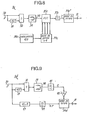
- the transmission part 1 of the device shown in FIG. 1 comprises a series-parallel converter 10, a frequency multiplication circuit 11, a phase shift circuit 12 and a modulation circuit 13.
- Two input terminals 100 and 101 of the converter 10 receive in synchronism a clock signal H and a serialized informative binary signal B shown in the first and second lines of FIG. 2.
- the clock signal H has a rhythm period T equal to that of the binary signal B.
- the converter 10 demultiplexes the binary signal B into two synchronous binary signals bl and b2 which correspond to the bits of odd and even rank of the signal B as shown in the third and fourth lines of FIG. 2.
- Each bit of the signals b 1 and b 2 occupies an elementary interval T equal to 2T, called the modulation period.
- the converter 10 also restores an H / 2 clock signal having the period 2T.
- the signals b i , b 2 and H / 2 are applied to three inputs 130, 131 and 132 of the modulation circuit 13.
- the input terminal 100 is also connected to an input of the frequency multiplication circuit 11 which multiplies the frequency 1 / T of the clock signal H by a factor n to restore a carrier P at the frequency n / T.
- circuit 11 generates carrier P in different ways.
- the circuit 11 is a conventional frequency divider in which the division is carried out by logic circuits.
- the circuit 11 contains an analog multiplier or a phase locked loop.
- the circuit It preferably contains a phase locked loop. In all cases, the carrier P is generated directly from the clock signal H and is therefore synchronous with it.
- the factor n is equal to 3/2 and that the carrier P is in the form of a pulse signal of duty cycle 0.5.
- the carrier can be a sine wave.
- the phase shifter circuit 12 produces from the carrier P delivered by the circuit 11 four digital signals ⁇ 0, ⁇ 1, 02 and ⁇ 3 which are at the same frequency n / T and which are applied to four inputs 133 to 136 of the modulation circuit 13
- the signals ⁇ 0, ⁇ 1, ⁇ 2 and ⁇ 3 are signals coming from the carrier P and phase shifted with respect to this one of 0, ⁇ / 2, ⁇ and 3 ⁇ / 2 respectively in order to produce a signal with quadrivalent modulation S in the circuit 13.
- the four pairs of bits of the signals b, and b 2 such as 00, 01, 10 and 11 correspond in the signal S to elements of the carrier P having the duration T , constituted by the respective phase-shifted signals ⁇ 0, ⁇ 1, ⁇ 2 and ⁇ 3.
- the signal S at the output 137 of the modulation circuit 13 is shown on the last line of FIG. 2.
- the receiving part of the device is designated as a whole by 2 in FIG. 3.
- the modulated signal S transmitted by the transmission part 1 is received at the input 200 of an equalization circuit 20.
- the circuit 20 in particular compensates for amplitude and phase distortions due to the transmission means conveying the signal S between parts 1 and 2, and bandpass filtering and preamplification of the channel in which the signal S is transmitted.
- the transmission means can be a cable or optical fiber link, or a radio link.
- the equalized signal S 'delivered by the output 201 of the circuit 20 is supplied to the inputs 210, 220 of two demodulation circuits 21 and 22 and to the input 30 of a circuit for recovering the carrier frequency and the frequency of rhythm 3.
- Circuit 3 extracts a carrier whose phase is perfectly known with respect to the carrier produced in the transmission part 1. From the extracted carrier, an output bus 31 of circuit 3 supplies two other inputs 211 , 221 of the demodulation circuits 21, 22 two carriers recovered in quadrature P and P - ⁇ / 2 so that the outputs 212 and 222 of the circuits 21 and 22 restore two demodulated signals which contain the binary information corresponding to the signals b and b 2 processed in the transmission part 1. The demodulated signals are then applied to two filter circuits 24 and 25 which eliminate the residues of the demodulations and filter the demodulated signals according to the Nyquist criterion.
- the regenerated binary signals b and b 2 are applied to two inputs 281, 282 of a parallel-serial converter 28, another input 283 of which receives the clock signal H at the rhythm frequency 1 / T supplied by the output bus 31 of the circuit 3.
- the converter 28 performs the reverse operation of the converter 10 and produces on a output 284 the initial informative binary signal B accompanied by the clock signal H on another output 285.
- the carrier P was produced independently of the clock signal, for example by a local oscillator, and was therefore not in synchronism with the clock signal.
- the transmission part according to the prior art included a transcoder of the binary signals b and b 2 inserted between the circuits 10 and 13 and generally allowing differential modulation.
- the carrier recovery circuit recovered only the carrier without being able to recover the clock signal H, since from the modulated signal received, a carrier can be recovered by multiplication by 4 then divide by 4 in frequency without its phase being perfectly determined with respect to that of the transmission part.
- phase shift equal to an integer multiple of ⁇ / 2 between the recovered carrier and the carrier in the transmission part.
- the phase ambiguity due to the reconstitution of the carrier was then removed by a transcoder inserted between circuits 26 and 27 and circuit 28.
- the clock signal was recovered from the demodulated signals at the outputs of circuits 24 and 25.
- the modulated signal S 'delivered by circuit 20 at input 30 is applied directly to a first input 320 of an analog summing circuit 32 and through a delay 33 at a second input 321 of circuit 32.
- the delay circuit 33 imposes a delay equal to T / 2 and supplies the signal S '+ T / 2 shown in the second line of FIG. 5.
- the summing circuit 32 is assumed here to be an analog adder which adds the signals S 'and S' + T / 2 into a summing signal S '+ (S' + T / 2) which is applied to the input 340 of a full-wave rectifier 34.
- the summation signal at the input 340 of the rectifier 34 is a three-level signal.
- the summation signal results from the sum of two carrier elements phase shifted by 0, ⁇ / 2, ⁇ or 3 ⁇ / 2.
- the summation signal results from the sum of two carrier elements phase shifted by T r thanks to the delay circuit 33.
- the signal rectified at the output 341 of the rectifier 34 shown in the fourth line of FIG. 5 thus presents in the second half-periods a constant level reduced to zero whatever the sequence of the carrier elements, that is to say of the composition of the initial binary signal B.
- the zero level is shown diagrammatically by a zero d energy in the fifth line of Fig. 5 which is recurrent in period T and whose location in each modulation period T is well determined, here three quarters from the start of period T.
- the summing circuit 32 can be constituted by an analog subtractor without modifying the principle of the recovery of the carrier according to the invention. Indeed, in an elementary modulation interval T the carrier P keeps a constant phase. Depending on whether the ratio 2n between the frequency of the carrier P and the modulation frequency 1 / T is odd or even, it is respectively necessary to operate an addition or a subtraction between the signal S 'and the delayed signal S' + T / 2. In these conditions appears a zero energy of period T , therefore a frequency component 1 / T.
- the other circuits making up the circuit for recovering carrier frequencies and timing 3a are equivalent to a slave loop which essentially aims to filter or synthesize the carrier from the zero of periodic energy at output 341, the phase of the carrier thus filtered being perfectly determined with respect to the reference phase of the carrier in the transmission part. From this recovered carrier are then produced in particular clock signals necessary for the regeneration of the binary signal B.
- a sampling circuit 35a receives the rectified signal from the output 341 of the rectifier 34 and samples the latter on either side of the energy zeros under the control of logic sampling signals E 1 and E 2 supplied. on two outputs 391 of a time base 39a and shown in the sixth and seventh lines of FIG. 5.
- the signals E 1 and E 2 are at period T and have respectively pulses having a width T / 4 on either side of the energy zeros.
- the signals E l and E 2 are obtained from the carrier recovered in the time base 39a.
- Two outputs 350 of circuit 35a establish two sample signals e 1 and e 2 shown in the last two lines of FIG.
- the signals e 1 and e 2 have a continuous component which translates the phase difference between the carrier wave established at the output 341 of the rectifier shown in the fifth line FIG. 5, and the signals E 1 and E 2 of the time base 39a.
- the differential processing in the amplifier 36a and the low-pass filtering in the filter 37a provide the error signal necessary for the operation of the slave loop.
- the sampling circuit 35a and the differential amplifier 36a carry out an analog phase comparator.
- the filtered signal leaving the filter 37a is then applied to the control input 380 of a voltage controlled oscillator (VCO) 38a which oscillates at the frequency 4 / T with a phase controlled by that of the signal at the output 341.
- VCO voltage controlled oscillator
- a signal at frequency 4 / T at output 381 of oscillator 38a is supplied to input 390 of time base 39a which, as already said, produces the control signals for sampling E and E 2 and recovered carrier and recovered rhythm signals at frequencies 1 / T , n / T, 1 / T and 2 / T on two outputs 391 connected to the sampling circuit 35a and on the bus 31 connected to the demodulation circuits 21 and 22 , to the regeneration circuits 26 and 27 and to the parallel-series converter 28 (Fig. 3).
- the signal S ' is composed of two elementary intervals with a carrier of amplitude peak to peak between -3 and +3 with two phases 0 and ⁇ and two elementary intervals with a carrier of peak-to-peak amplitude between +1 and -1 with two phases 0 and ⁇ .
- the processing of the carrier at the output 341 of the rectifier is then independent of the phase or amplitude modulation.
- the signal S ' will be independently considered in phase or amplitude modulation.
- circuits 32 to 39a are found in detailed form.
- the delay circuit 33 consists of an all-pass filter with two operational amplifiers in cascade 331 and 332, and delays the signal S 'by T / 2.
- the amplifier 331 is associated at the input with a double T cell 333 and in feedback with a T cell 334.
- the output of the amplifier 332 and the input 30 of the recovery circuit are respectively connected to the two input terminals 321 and 320 of an analog subtractor circuit with operational amplifier 322 included in the circuits 32 and 34.
- the amplifier 322 is provided with two feedback loops each composed of a set with a resistor 342 and a diode 343. The diodes are mounted head to tail.
- the amplifier circuit 322 thus operates both as a subtractor to produce the summation signal S '- (S' + T / 2) and as a monoalternation rectifier.
- the signals rectified at the common terminals of the resistors 342 and of the diodes 343 are then subtracted in a subtractor with operational amplifier 346 which produces on its output 341 the rectified signal with full alternation.
- the sampling circuit 35a of the circuit 3a includes two switches 351. Each switch 351 is in series with a resistor 352 between the output 341 of the amplifier 346 of the summing and rectifying circuit 32 - 34 and the ground. The common terminal of each resistor 352 and of the respective switch 351 is connected through an input resistor to one of the terminals 36-, 36 + of an operational amplifier 361 included in the differential amplifier 36a.
- the switches 351 carry out the sampling according to the principle of the diagrams in the last four lines of FIG. 5.
- the differential processing in amplifier 361 performs an analog phase comparison. Low-pass filtering in circuits 36a and 37a is provided before closing the servo loop on oscillator 38a.
- the frequency signal 4 / ⁇ at the output 381 of the amplifier 382 is applied to the clock inputs 390 of two flip-flops of the D type 393 and 394 included in the time base 39a.
- the complementary output Q4 of the second flip-flop 394 is connected to the input D3 of the first flip-flop 393.
- the output Q3 of the flip-flop 393 is connected to the input D4 of flip-flop 394.
- One of the inputs of each of two NAND gates 396 and 397 included in the time base 39a is connected to the output Q3 of the first flip-flop 393.
- the other inputs of the gates 396 and 397 are connected respectively to the outputs Q4 and Q4 of the second flip-flop 394.
- the outputs 391 of gates 396 and 397 deliver the two sampling control signals E and E 2 shown in the sixth and seventh lines of FIG. 5 to control the two switches 351.
- the outputs Q3 and Q4 are connected to the second inputs of the modulation circuits 21 and 22 to supply the two carriers returned in quadrature used for demodulation.
- a second example of a circuit 3b recovering the carrier frequency and the rhythm frequency from a signal modulated in phase or in amplitude S ' is shown in detail in FIG. 7.
- the rhythm frequency I / T and the frequency of the carrier P are equal to 152 kHz and 76 kHz, as for the embodiment illustrated in FIG. 6.
- the circuit 3b comprises, after the input 30, a delay circuit 33 and a full-wave summation and rectification circuit 32 - 34 identical to those already described with reference to FIG. 6.
- the circuit 3b differs from the circuit 3a essentially by the structure of the control loop 35b - 39b which includes a logic phase comparator 36b equivalent to an OR-EXCLUSIVE operator.
- the sampling circuit 35b is mainly constituted by a band-pass filter with switched capacities 353 with frequency tuned to 76 kHz.
- the filter 353 comprises an RC network whose resistor 354 is inserted between the output 341 of the amplifier 346 and the output terminal 355 of the filter 353 which is common to four parallel capacitive assemblies. Each capacitive assembly is composed of a switch 356 and a capacitor 357 in series between the terminal 355 and the ground. Sampling at the frequency 1 / T is obtained by successive closings of the four switches 354 during a period T / 4.
- the output terminal 355 of the filter 353 is connected to the second order bandpass filter with operational amplifier 358 which eliminates the sampling residues.
- a Schmitt flip-flop 359 is provided between the output of the operational amplifier of the filter 358 and an input 36 of the phase comparator 36b. The flip-flop 359 returns the filtered signal to the modulation frequency as pulses.
- the other input 36, of the phase comparator 36b is linked to the output Q4 of a flip-flop 394 of the time base 39b delivering a signal at the modulation frequency 1 / T.
- the time base 39b includes two D-type flip-flops 393 and 394 and an EXCLUSIVE door 395 which are arranged in the same way as in the time base 39a shown in FIG. 6.
- the low-pass filter 37b comprises an active filter with operational amplifier 371 which is connected to the output 360 of the phase comparator 36b, and a low-pass cell 372 which is connected to the output of the amplifier 371.
- the signal filtered error is applied to the control input 380 of the oscillator 38b which is of the conventional quartz oscillator 384 voltage controlled (VCXO) and operational amplifier 385 type.
- the output 381 of the amplifier 385 is connected to the inputs clock 390 of toggles 393 and 394 of time base 39b.
- the corresponding recovery circuits 3c and 3d are based on the same principle as that 3a in FIG. 4, namely a return of carrier by delay, addition and rectifications
- the circuits 3c and 3d therefore comprise from the input 30, the summing circuit 32, the delay circuit 33 and the full-wave rectifier 34 arranged in the same as in circuit 3a.
- the phase loop 35a to 39a of FIG. 4 is replaced by a local oscillator 38c, a time base 39c with frequency division by 4 and a filter with four switched capacitors 35c.
- the local oscillator 38c delivers a signal at the frequency 4 / T.
- the time base 39c divides by four the frequency of the signal leaving the oscillator 38c and provides four sampling control signals at the frequency 1 / T and phase shifted by ir / 2 with respect to each other.
- the filter 35c samples the rectified signal at output 341 of the rectifier 34 under the control of the time base 39c.
- the sampled signal leaving the filter 35c is filtered low pass in a filter 37c which restores the carrier P from which the signals necessary for demodulation and the rhythm signals H and H / 2 are produced in a time base 39c ' on the bus 31.
- the circuits 35c, 37c, 38c and 39c are of the same type as those 35b, 37b, 3.8b and 39b shown in detail in FIG. 7.
- the carrier wave is directly filtered.
- the first embodiment (Fig. 4) there is synthesis of the carrier wave with a phase control relative to the signal at the output 341 of the rectifier 34; under these conditions, a phase shift is always possible.
- the circuit 3c of FIG. 8 avoids this drawback.
- the production of the rhythm frequencies H and H / 2 requires a second time base 39c '.
- the circuit for recovering the carrier frequency and the 3d rhythm frequency shown in FIG. 9 presents two leads.
- the first derivation comprises, from the input 30, the assembly 32, 33 and 34, a narrow-band bandpass filter 41 and a Schmitt flip-flop 42.
- the filter 41 is tuned to the frequency P and restores the carrier P which is shaped by the rocker 42.
- the rising front of the pulses leaving the flip-flop 42 stalls in phase a frequency divider by 4 included in a time base 39d.
- the multiplier 43 eliminates the phase modulation in the signal S 'and the filter 44 restores a pure signal at the frequency 4P as a function of which the time base 39c develops by division the corresponding signals on the bus 3I.
- the fourth embodiment has the advantage that the time base 39d permanently receives a signal at the frequency IP which is independent of the state of the modulation elements in the signal S ', that is to say of the state bits of signal B. No loss of rhythm frequency takes place in the time base 39d.
- the recovery circuits 3a to 3c are dependent on the statistics of the binary signal B and more precisely on long sequences of bits of the same binary state which produce a constant energy level in the rectified signal (Fig. 5 , fourth and fifth lines) which prevents the carrier from being reconstructed by phase comparison and filtering.
- This loss of rhythm is avoided in the 3d circuit, since the carrier P formed by the flip-flop 42 only serves to stall the phase in the time base 39d.
- the implementation of the 3d circuit does not require the use of scrambler on transmission and scrambler on reception to make the modulation signal pseudo-random, as according to the prior art.
Abstract
L'invention vise à simplifier les modems en rendant la porteuse synchrone du signal de rythme à l'émission et en récupérant à la réception une porteuse dont la phase est cohérente avec le signal de rythme. Le taux d'erreurs est diminué puisque le transcodage est supprimé. L'immunité au bruit est améliorée puisqu'il est possible de réaliser une démodulation cohérente. Une seule restitution de rythme est suffisante, ce qui améliore le comportement en gigue. Le dispositif de récupération comprend un circuit (33) pour retarder le signal de modulation reçu d'un retard égal à la moitié de la période de modulation, un circuit (32) pour sommer les signaux reçu et retardé, et un redresseur (34) pour redresser à double alternance le signal de sommation en un signal redressé en vue de l'appliquer à l'appliquer à l'entrée d'une boucle de verrouillage (35a-39a) à circuit d'échantillonnage, comparateur de phase, en filtre passe-bas et oscillateur commandé en tension.The invention aims to simplify the modems by making the carrier synchronous with the rhythm signal on transmission and by recovering on reception a carrier whose phase is consistent with the rhythm signal. The error rate is reduced since transcoding is eliminated. The noise immunity is improved since it is possible to carry out a coherent demodulation. A single rhythm restitution is sufficient, which improves the jitter behavior. The recovery device comprises a circuit (33) for delaying the received modulation signal by a delay equal to half the modulation period, a circuit (32) for summing the received and delayed signals, and a rectifier (34) for rectifying the summation signal at full alternation into a rectified signal with a view to applying it to applying it to the input of a locking loop (35a-39a) with sampling circuit, phase comparator, as filter low pass and voltage controlled oscillator.
Description
L'invention a trait d'une manière générale aux modems de système de transmission numérique fondés sur une modulation de phase de la porteuse en 2, 4 ou 8 états de phase, bien que l'invention s'applique également à la modulation d'amplitude de la porteuse en plusieurs états d'amplitude.The invention relates generally to digital transmission system modems based on a phase modulation of the carrier in 2, 4 or 8 phase states, although the invention also applies to the modulation of carrier amplitude in several amplitude states.
Plus particulièrement, l'invention concerne un dispositif de récupération des fréquences de porteuse et de rythme pour des transmissions numériques comprenant à l'émission, des moyens recevant un signal binaire, un signal à la fréquence de rythme du signal binaire et une porteuse dont la fréquence P est dans un rapport n prédéterminé avec la fréquence de rythme 1/T pour moduler en phase ou en amplitude la porteuse par le signal binaire en un signal de modulation définie par I = 21 états de phases ou d'amplitude qui correspondent à des combinaisons de J bits successifs du signal binaire modulant, et ayant une fréquence de modulation 1/T égale à 1/JT, et à la réception, des moyens comprenant une boucle de verrouillage incluant en série un comparateur de phase, un filtre passe-bas et un oscillateur commandé en tension pour récupérer la fréquence P de la porteuse à partir du signal de modulation en vue de démoduler en phase ou en amplitude le signal de modulation en le signal binaire et de récupérer la fréquence de rythme.More particularly, the invention relates to a device for recovering carrier and rhythm frequencies for digital transmissions comprising on transmission, means receiving a binary signal, a signal at the rhythm frequency of the binary signal and a carrier whose frequency P is in a predetermined relationship n with the frequency of
Dans les systèmes de modulation à états de phase et de démodulation cohérente de ce type, la porteuse est produite à l'émission par un oscillateur local dont la phase est indéterminée par rapport au signal de rythme. A la réception, la plupart des moyens de récupération de la porteuse comprennent un multiplicateur de fréquence par I du signal de modulation afin d'éliminer la modulation de phase et récupérer un signal à la fréquence pure IP. Une boucle de verrouillage de phase permet d'asservir un oscillateur commandé en tension à la fréquence IP et de récupérer une porteuse synchrone de la porteuse d'émission après une division en fréquence par I en sortie de la boucle de verrouillage. Cependant, la phase de la porteuse récupérée n'est pas déterminée par rapport au signal de rythme pour procéder à la démodulation du signal reçu. En effet, la phase de la porteuse récupérée à la sortie du diviseur de fréquence s'initialise spontanément à l'une des I phases définies par la modulation.In phase-state modulation and coherent demodulation systems of this type, the carrier is produced on transmission by a local oscillator whose phase is indeterminate with respect to the signal. of rhythm. On reception, most of the carrier recovery means include a frequency multiplier by I of the modulation signal in order to eliminate the phase modulation and recover a signal at the pure frequency IP. A phase locking loop makes it possible to control a voltage-controlled oscillator at the frequency IP and to recover a synchronous carrier from the transmission carrier after a frequency division by I at the output of the locking loop. However, the phase of the recovered carrier is not determined with respect to the timing signal to demodulate the received signal. Indeed, the phase of the carrier recovered at the output of the frequency divider spontaneously initializes to one of the I phases defined by the modulation.
Pour lever l'ambiguïté de phase à la réception et donc retrouver les suites de bits du signal binaire respectivement en fonction des états de phase correspondants, il est fait appel à un transcodage des J trains binaires correspondant aux bits de même rang dans les suites à J bits du signal binaire. Le transcodage peut être une modulation de phase différentielle (DPSK) ou bien un codage particulier, tel que retard sur l'un des trains binaires ou insertion d'un mot binaire particulier, afin de lever l'ambiguïté de phase dans un transcodeur à la réception. La complexité du transcodeur augmente en fonction du nombre I d'états de phase et affecte au moins la moitié du coût du modem. Le transcodage multiplie également le nombre des erreurs.To remove the phase ambiguity on reception and therefore recover the bit streaks of the binary signal respectively as a function of the corresponding phase states, transcoding of the J bit strings corresponding to the bits of the same rank in the streaks is used. J bits of the binary signal. The transcoding can be a differential phase modulation (DPSK) or a particular coding, such as delay on one of the binary trains or insertion of a particular binary word, in order to remove the phase ambiguity in a transcoder at the reception. The complexity of the transcoder increases as a function of the number I of phase states and affects at least half the cost of the modem. Transcoding also multiplies the number of errors.
La présente invention a pour but de simplifier la composition des modems connus en rendant la porteuse synchrone du signal de rythme à l'émission et par suite, en récupérant à la réception une porteuse dont la phase est cohérente avec le signal de rythme à l'émission. Les transcodages à l'émission et à la réception selon la technique antérieure sont supprimés. Le poids et le coût du modem selon l'invention sont alors réduits et corollairement la fiabilité du modem est augmentée. Le taux d'erreurs est diminué puisque le transcodage qui multiplie les erreurs est supprimé. L'immunité au bruit est améliorée du fait qu'il est possible de réaliser une démodulation cohérente. La récupération de rythme est simplifier : une seule restitution de rythme est suffisante au lieu de J restitutions de rythme, ce qui améliore le comportement en gigue.The object of the present invention is to simplify the composition of known modems by making the carrier synchronous with the timing signal on transmission and consequently by recovering on reception a carrier whose the phase is consistent with the timing signal on transmission. Transcoding on transmission and reception according to the prior art is eliminated. The weight and the cost of the modem according to the invention are then reduced and consequently the reliability of the modem is increased. The error rate is reduced since the transcoding which multiplies the errors is eliminated. Noise immunity is improved because it is possible to perform coherent demodulation. Rhythm recovery is simplified: a single rhythm restitution is sufficient instead of J rhythm restitution, which improves the jitter behavior.
A ces fins, l'invention a pour objet un dispositif de récupération des fréquences porteuse et de rythme du type défini dans l'entrée en matière, caractérisé en ce qu'il comprend à l'émission, des moyens pour multiplier en fréquence par le rapport n le signal de rythme en la porteuse, et en ce qu'à la réception, les moyens pour récupérer la porteuse comprennent des moyens pour retarder le signal de modulation d'un retard égal à la moitié de la période de modulation T, des moyens pour sommer le signal de modulation et le signal de modulation retardé en un signal de sommation, et des moyens pour redresser à double alternance le signal de sommation en un signal redressé en vue de l'appliquer à l'entrée de la boucle de verrouillage.For these purposes, the subject of the invention is a device for recovering the carrier and rhythm frequencies of the type defined in the introduction, characterized in that it comprises, on transmission, means for multiplying in frequency by the report n the rhythm signal in the carrier, and in that on reception, the means for recovering the carrier comprise means for delaying the modulation signal by a delay equal to half of the modulation period T , means for summing the modulation signal and the delayed modulation signal into a summation signal, and means for rectifying the summation signal at full alternation into a rectified signal in order to apply it to the input of the locking loop .
D'autres caractéristiques et avantages de l'invention apparaîtront plus clairement à la lecture de la description suivante de plusieurs modes de réalisation de l'invention en référence aux dessins annexés correspondants, dans lesquels :
- - la Fig. 1 est un bloc-diagramme schématique de la partie d'émission d'un dispositif pour transmision à modulation à 4 états de phase selon l'invention ;
- - la Fig. 2 est un diagramme de formes d'onde produites dans la partie d'émission ;
- - la Fig. 3 est un bloc-diagramme schématique de la partie de réception du système de transmission ;
- - la Fig. 4 est un bloc-diagramme du circuit de récupération de la fréquence de porteuse et de la fréquence de rythme selon une première réalisation, inclus dans la partie de réception de la Fig. 3 ;
- - la Fig. 5 est un diagramme de formes d'onde produites dans le circuit de récupération de la Fig. 4 ;
- - la Fig. 6 est un bloc-diagramme plus détaillé du circuit de récupération de la Fig. 4 ;
- - La Fig. 7 est un bloc-diagramme détaillé d'un circuit de récupération de la fréquence de porteuse et de la fréquence de rythme selon une seconde réalisation quelque peu différente de la première ;
- - la Fig. 8 est un bloc-diagramme du circuit de récupération de la fréquence de porteuse et de la fréquence de rythme selon une troisième réalisation ; et
- - la Fig. 9 est un bloc-diagramme du circuit de récupération de la fréquence de porteuse et de la fréquence de rythme selon une quatrième réalisation.
- - Fig. 1 is a schematic block diagram of the transmission part of a device for modulated transmission with 4 phase states according to the invention;
- - Fig. 2 is a diagram of waveforms produced in the emission part;
- - Fig. 3 is a schematic block diagram of the reception part of the transmission system;
- - Fig. 4 is a block diagram of the circuit for recovering the carrier frequency and the rhythm frequency according to a first embodiment, included in the reception part of FIG. 3;
- - Fig. 5 is a diagram of waveforms produced in the recovery circuit of FIG. 4;
- - Fig. 6 is a more detailed block diagram of the recovery circuit of FIG. 4;
- - Fig. 7 is a detailed block diagram of a circuit for recovering the carrier frequency and the rhythm frequency according to a second embodiment somewhat different from the first;
- - Fig. 8 is a block diagram of the circuit for recovering the carrier frequency and the rhythm frequency according to a third embodiment; and
- - Fig. 9 is a block diagram of the circuit for recovering the carrier frequency and the rhythm frequency according to a fourth embodiment.
En référence aux Figs. 1 à 5 est décrit un dispositif de récupération des fréquences porteuses et de rythme pour transmission numérique à modulation de phase quadrivalente et à démodulation cohérente.With reference to Figs. 1 to 5 is described a device for recovering carrier frequencies and timing for transmission digital with quadrivalent phase modulation and coherent demodulation.
La partie d'émission 1 du dispositif montrée à la Fig. 1 comprend un convertisseur série-parallèle 10, un circuit de multiplication de fréquence 11, un circuit déphaseur 12 et un circuit de modulation 13.The
Deux bornes d'entrée 100 et 101 du convertisseur 10 reçoivent en synchronisme un signal d'horloge H et un signal binaire informatif sérialisé B montrés aux première et seconde lignes de la Fig. 2. Le signal d'horloge H a une période de rythme T égale à celle du signal binaire B. Le convertisseur 10 démultiplexe le signal binaire B en deux signaux binaires synchrones bl et b2 qui correspondent aux bits de rangs impair et pair du signal B comme montré aux troisième et quatrième lignes de la Fig. 2. Chaque bit des signaux b1 et b2 occupe un intervalle élémentaire T égal à 2T, appelé période de modulation. Le convertisseur 10 restitue également un signal d'horloge H/2 ayant la période 2T. Les signaux bi, b2 et H/2 sont appliqués à trois entrées 130, 131 et 132 du circuit de modulation 13.Two
La borne d'entrée 100 est également reliée à une entrée du circuit de multiplication de fréquence 11 qui multiplie la fréquence 1/T du signal d'horloge H par un facteur n pour restituer une porteuse P à la fréquence n/T. Suivant la valeur du facteur n, le circuit 11 engendre la porteuse P de différentes façons. Lorsque n < 1, le circuit 11 est un diviseur de fréquence classique dans lequel la division est réalisée par des circuits logiques. Lorsque n est entier et supérieur à l'unité, le circuit 11 contient un multiplicateur analogique ou une boucle à verrouillage de phase. Lorsque n est fractionnaire et supérieur à l'unité, le circuit Il contient de préférence une boucle à verrouillage de phase. Dans tous les cas, la porteuse P est engendrée directement à partir du signal d'horloge H et est donc synchrone avec celui-ci. Selon l'exemple illustré, il est présumé, comme montré à la cinquième ligne de la Fig. 2, que le facteur n est égal à 3/2 et que la porteuse P est sous la forme d'un signal d'impulsions de rapport cyclique 0,5. Cependant, la porteuse peut être une onde sinusoïdale. Ainsi selon cet exemple, la période de modulation T = 2T est égale à trois périodes p de la porteuse P.The
Le circuit déphaseur 12 produit à partir de la porteuse P délivrée par le circuit 11 quatre signaux numériques Ø0, Ø1, 02 et Ø3 qui sont à la même fréquence n/T et qui sont appliqués à quatre entrées 133 à 136 du circuit de modulation 13. Les signaux Ø0, Ø1, Ø2 et Ø3 sont des signaux issus de la porteuse P et déphasés par rapport à celle-ci de 0, π/2, π et 3π/2 respectivement afin de produire un signal à modulation quadrivalente S dans le circuit 13. Aux quatre paires de bits des signaux b, et b2 telles que 00, 01, 10 et 11 correspondent dans le signal S des éléments de la porteuse P ayant la durée T, constitués par les signaux déphasés respectifs Ø0, Ø1, Ø2 et Ø3. Le signal S à la sortie 137 du circuit de modulation 13 est montré à la dernière ligne de la Fig. 2.The phase shifter circuit 12 produces from the carrier P delivered by the
La partie de réception du dispositif est désignée dans son ensemble par 2 dans la Fig. 3. Le signal modulé S transmis par la partie d'émission 1 est reçu à l'entrée 200 d'un circuit d'égalisation 20. Le circuit 20 effectue notamment une compensation de distorsions d'amplitude et de phase dues au moyen de transmission véhiculant le signal S entre les parties 1 et 2, et un filtrage passe-bande et une préamplification du canal dans lequel est transmis le signal S. Le moyen de transmission peut être une liaison par câble ou fibre optique, ou une liaison hertzienne. Le signal égalisé S' délivré par la sortie 201 du circuit 20 est fourni aux entrées 210, 220 de deux circuits de démodulation 21 et 22 et à l'entrée 30 d'un circuit de récupération de la fréquence de porteuse et de la fréquence de rythme 3. Le circuit 3 extrait une porteuse dont la phase est parfaitement connue par rapport à la porteuse produite dans la partie d'émission 1. A partir de la porteuse extraite, un bus de sortie 31 du circuit 3 délivre à deux autres entrées 211, 221 des circuits de démodulation 21, 22 deux porteuses récupérées en quadrature P et P - π/2 afin que les sorties 212 et 222 des circuits 21 et 22 restituent deux signaux démodulés qui contiennent les informations binaires correspondant aux signaux b et b2 traités dans la partie d'émission 1. Les signaux démodulés sont appliqués ensuite à deux circuits de filtrage 24 et 25 qui éliminent les résidus des démodulations et filtrent les signaux démodulés selon le critère de Nyquist. Les signaux sortant des circuits 24 et 25 sont appliqués à des entrées 260, 270 de deux circuits de régénération 26 et 27 dont les autres entrées 261 et 271 reçoivent un signal d'horloge récupéré à la fréquence de modulation 1/T = 1/(2T) fourni par le bus de sortie 31 du circuit 3. Les signaux binaires b et b2 régénérés sont appliqués à deux entrées 281 , 282 d'un convertisseur parallèle-série 28 dont une autre entrée 283 reçoit le signal d'horloge H à la fréquence de rythme 1/T fourni par le bus de sortie 31 du circuit 3. Le convertisseur 28 effectue l'opération inverse du convertisseur 10 et produit sur une sortie 284 le signal binaire informatif initial B accompagné du signal d'horloge H sur une autre sortie 285.The receiving part of the device is designated as a whole by 2 in FIG. 3. The modulated signal S transmitted by the
Comparativement à la technique antérieure, dans la partie de réception, la porteuse P était produite indépendamment du signal d'horloge, par exemple par un oscillateur local, et n'était donc pas en synchronisme avec le signal d'horloge. Afin de connaître la phase de référence de la porteuse à la réception, la partie d'émission selon la technique antérieure comprenait un transcodeur des signaux binaires b et b2 inséré entre les circuits 10 et 13 et permettant une modulation différentielle généralement. Dans la partie de réception selon la technique antérieure, le circuit de récupération de la porteuse ne récupérait que la porteuse sans pouvoir récupérer le signal d'horloge H, puisqu'à partir du signal modulé reçu, une porteuse peut être récupérée par multiplication par 4 puis division par 4 en fréquence sans que sa phase ne soit parfaitement déterminée par rapport à celle de la partie d'émission. Cette indétermination est traduite par un déphasage égal à un multiple entier de π/2 entre la porteuse récupérée et la porteuse dans la partie d'émission. L'ambiguïté de phase due à la reconstitution de la porteuse était alors levée par un transcodeur inséré entre les circuits 26 et 27 et le circuit 28. Le signal d'horloge était récupéré à partir des signaux démodulés aux sorties des circuits 24 et 25.Compared to the prior art, in the reception part, the carrier P was produced independently of the clock signal, for example by a local oscillator, and was therefore not in synchronism with the clock signal. In order to know the reference phase of the carrier on reception, the transmission part according to the prior art included a transcoder of the binary signals b and b 2 inserted between the
En référence aux Figs. 4 et 5, on décrit maintenant le circuit de récupération de la fréquence de porteuse et de la fréquence de rythme 3a selon une première réalisation. Le signal modulé S' délivré par le circuit 20 à l'entrée 30 est appliqué directement à une première entrée 320 d'un circuit de sommation analogique 32 et à travers un circuit de retard 33 à une seconde entrée 321 du circuit 32. Le circuit de retard 33 impose un retard égal à T/2 et fournit le signal S' + T/2 montré à la seconde ligne de la Fig. 5. Le circuit de sommation 32 est supposé être ici un additionneur analogique qui additionne les signaux S' et S' + T/2 en un signal de sommation S'+ (S' + T/2) qui est appliqué à l'entrée 340 d'un redresseur à double alternance 34. Comme cela apparaît à la troisième ligne de la Fig. 5, le signal de sommation à l'entrée 340 du redresseur 34 est un signal à trois niveaux. Dans la première demi-période T/2 de chaque période de modulation, le signal de sommation résulte de la somme de deux éléments de porteuse déphasés de 0, π/2, π ou 3π/2. Dans la seconde demi-période T/2 de chaque période de modulation, le signal de sommation résulte de la somme de deux éléments de porteuse déphasés de Tr grâce au circuit de retard 33. Le signal redressé à la sortie 341 du redresseur 34 montré à la quatrième ligne de la Fig. 5 présente ainsi dans les secondes demi-périodes un niveau constant ramené à zéro quelle que soit la suite des éléments de porteuse, c'est-à-dire de la composition du signal binaire initial B. Le niveau zéro est schématisé par un zéro d'énergie dans la cinquième ligne de la Fig. 5 qui est récurrent à la période T et dont l'emplacement dans chaque période de modulation T est bien déterminé, ici aux trois quarts à partir du début de la période T.With reference to Figs. 4 and 5, the circuit for recovering the carrier frequency and the
Cependant, en dépendance du facteur n, le circuit de sommation 32 peut être constitué par un soustracteur analogique sans modifier le principe de la récupération de la porteuse selon l'invention. En effet, dans un intervalle élémentaire de modulation T la porteuse P garde une phase constante. Selon que le rapport 2n entre la fréquence de la porteuse P et la fréquence de modulation 1/T est impair ou pair, il faut respectivement opérer une addition ou une soustraction entre le signal S' et le signal retardé S' + T/2. Dans ces conditions apparaît un zéro d'énergie de période T, donc une composante de fréquence 1/T.However, depending on the factor n, the summing
Les autres circuits composant le circuit de récupération des fréquences de porteuse et de rythme 3a sont équivalents à une boucle asservie qui a pour but essentiellement de filtrer ou de synthétiser la porteuse à partir du zéro d'énergie périodique à la sortie 341, la phase de la porteuse ainsi filtrée étant parfaitement déterminée par rapport à la phase de référence de la porteuse dans la partie d'émission. A partir de cette porteuse récupérée sont ensuite produits notamment des signaux d'horloge nécessaires à la régénération du signal binaire B.The other circuits making up the circuit for recovering carrier frequencies and
Lesdits autres circuits précités sont agencés suivant une boucle à verrouillage de phase 35a à 39a selon une première réalisation montrée à la Fig. 4. Un circuit d'échantillonnage 35a reçoit le signal redressé de la sortie 341 du redresseur 34 et échantillonne celui-ci de part et d'autre des zéros d'énergie sous la commande de signaux logiques d'échantillonnage E1 et E2 fournis sur deux sorties 391 d'une base de temps 39a et montrés aux sixième et septième lignes de la Fig. 5. Les signaux E1 et E2 sont à la période T et ont respectivement des impulsions ayant une largeur T/4 de part et d'autre des zéros d'énergie. Les signaux El et E2 sont obtenus a partir de la porteuse récupérée dans la base de temps 39a. Deux sorties 350 du circuit 35a établissent deux signaux d'échantillon e1 et e2 montrés aux deux dernières lignes de la Fig. 5, qui sont appliquées aux entrées 36 et 36+ d'un amplificateur différentiel 36a ayant une sortie 360 reliée à un filtre passe-bas 37a. Les signaux e1 et e2 ont une composante continue qui traduit l'écart de phase entre l'onde porteuse établie à la sortie 341 du redresseur montrée à la cinquième ligne Fig. 5, et les signaux E1 et E2 de la base de temps 39a. Le traitement différentiel dans l'amplificateur 36a et le filtrage passe-bas dans le filtre 37a fournissent le signal d'erreur nécessaire au fonctionnement de la boucle asservie. Au total, le circuit d'échantillonnage 35a et l'amplificateur différentiel 36a réalisent un comparateur de phase analogique. Le signal filtré sortant du filtre 37a est ensuite appliqué à l'entrée de commande 380 d'un oscillateur commandé en tension (VCO) 38a qui oscille à la fréquence 4/T avec une phase asservie à celle du signal à la sortie 341. Un signal à la fréquence 4/T à la sortie 381 de l'oscillateur 38a est fourni à l'entrée 390 de la base de temps 39a qui, comme déjà dit, produit les signaux de commande pour l'échantillonnage E et E2 et des signaux de porteuse récupérée et de rythme récupéré à des fréquences 1/T, n/T, 1/T et 2/T sur deux sorties 391 reliées au circuit d'échantillonnage 35a et sur le bus 31 relié aux circuits de démodulation 21 et 22, aux circuits de régénération 26 et 27 et au convertisseur parallèle-série 28 (Fig. 3).Said other aforementioned circuits are arranged in a phase locked
On notera que le principe de la récupération de la porteuse selon l'invention, représenté essentiellement par les fonctions des circuits 32, 33 et 34, est applicable à des modulations de phase ou d'amplitude d'un signal numérique quel que soit le nombre d'états de phase ou d'amplitude. Plus précisément, le principe de l'invention s'applique à tout signal modulé produit par la modulation de phase d'une onde porteuse définie par I = 2J états de phase qui correspondent respectivement aux I combinaisons possibles de J bits successifs du signal binaire B, et s'applique également à tout signal produit par une modulation d'amplitude d'une onde porteuse définie par I = 2J états d'amplitude qui correspondent respectivement aux I combinaisons possibles de J bits successifs du signal binaire B. Par exemple, pour quatre états d'amplitude +3, -3, +1 et -1, le signal S' est composé de deux intervalles élémentaires avec une porteuse d'amplitude crête à crête entre -3 et +3 avec deux phases 0 et π et deux intervalles élementaires avec une porteuse d'amplitude crête à crête entre +1 et -1 avec deux phases 0 et π. Le traitement de la porteuse à la sortie 341 du redresseur est alors indépendant de la modulation de phase ou d'amplitude. Dans la suite, en référence aux Figs. 6 à 9, le signal S' sera indépendamment considéré en modulation de phase ou d'amplitude.It will be noted that the principle of carrier recovery according to the invention, represented essentially by the functions of
Il est également à noter que la valeur du retard R = T/2 est très différente du retard égal à T utilisé pour la démodulation différentielle connue de chacun des signaux b1 et b2.It should also be noted that the value of the delay R = T / 2 is very different from the delay equal to T used for the known differential demodulation of each of the signals b 1 and b 2 .
La Fig. 6 montre la structure détaillée du circuit de récupération de la fréquence de porteuse et de la fréquence de rythme 3a pour une fréquence de rythme 1/T = 152 kHz, un facteur n = 0,5 et donc une fréquence de porteuse P = 76 kHz. La période de modulation est donc T = 2T = p. Dans la Fig. 6, on retrouve les circuits 32 à 39a sous forme détaillée.Fig. 6 shows the detailed structure of the recovery circuit of the carrier frequency and of the
Le circuit de retard 33 est constitué par un filtre passe-tout à deux amplificateurs opérationnels en cascade 331 et 332, et retarde le signal S' de T/2. L'amplificateur 331 est associé en entrée à une cellule en double T 333 et en contre-réaction à une cellule en T 334. La sortie de l'amplificateur 332 et l'entrée 30 du circuit de récupération sont respectivement reliées aux deux bornes d'entrée 321 et 320 d'un circuit soustracteur analogique à amplificateur opérationnel 322 inclus dans les circuits 32 et 34. L'amplificateur 322 est prévu avec deux boucles de réaction composées chacune d'un ensemble à une résistance 342 et une diode 343. Les diodes sont montées tête-bêche. Le circuit à amplificateur 322 fonctionne ainsi à la fois en soustracteur pour produire le signal de sommation S' - (S' + T/2) et en redresseur monoalternance. Les signaux redressés aux bornes communes des résistances 342 et des diodes 343 sont alors soustraits dans un soustracteur à amplificateur opérationnel 346 qui produit sur sa sortie 341 le signal redressé à double alternance.The
Le circuit d'échantillonnage 35a du circuit 3a comprend deux interrupteurs 351. Chaque interrupteur 351 est en série avec une résistance 352 entre la sortie 341 de l'amplificateur 346 du circuit sommateur et redresseur 32 - 34 et la masse. La borne commune de chaque résistance 352 et de l'interrupteur respectif 351 est reliée à travers une résistance d'entrée à l'une des bornes 36-, 36+ d'un amplificateur opérationnel 361 inclus dans l'amplificateur différentiel 36a. Les interrupteurs 351 réalisent l'échantillonnage selon le principe des diagrammes aux quatre dernières lignes de la Fig. 5. Le traitement différentiel dans l'amplificateur 361 réalise une comparaison de phase analogique. Le filtrage passe-bas dans les circuits 36a et 37a est prévu avant de refermer la boucle d'asservissement sur l'oscillateur 38a.The
L'oscillateur 38a est un oscillateur à pont de Wien comprenant un amplificateur opérationnel 382 et une diode à capacité variable 383 pour l'asservissement à la fréquence 4/T = 304 kHz. Le signal de fréquence 4/τ à la sortie 381 de l'amplificateur 382 est appliqué aux entrées d'horloge 390 de deux bascules bistables du type D 393 et 394 incluses dans la base de temps 39a. La sortie complémentaire Q4 de la seconde bascule 394 est reliée à l'entrée D3 de la première bascule 393. La sortie Q3 de la bascule 393 est reliée à l'entrée D4 de la bascule 394. Les signaux de sortie tels que Q3 et Q4 ou Q3 et Q4 des deux bascules 393 et 394 sont donc en quadrature et à la fréquence 1/τ = 76 kHz. L'une des entrées de chacune de deux portes NON-ET 396 et 397 incluses dans la base de temps 39a est reliée à la sortie Q3 de la première bascule 393. Les autres entrées des portes 396 et 397 sont reliées respectivement aux sorties Q4 et Q4 de la seconde bascule 394. Les sorties 391 des portes 396 et 397 délivrent les deux signaux de commande d'échantillonnage E et E2 montrés aux sixième et septième lignes de la Fig. 5 pour commander les deux interrupteurs 351. Les sorties Q3 et Q4 sont reliées aux secondes entrées des circuits de modulation 21 et 22 pour fournir les deux porteuses restituées en quadrature utilisées pour la démodulation. Les sorties Q3 et Q4 sont reliées aux entrées d'une porte OU-EXCLUSIF 395 dont la sortie délivre le signal de rythme H à la fréquence 2/T = 1/T en vue de le transmettre conjointement au signal H/2 à la sortie Q3 aux entrées 283, 261 et 271 des circuits 28, 26 et 27 (Fig. 3).
Un second exemple d'un circuit 3b récupérant la fréquence de porteuse et la fréquence de rythme à partir d'un signal modulé en phase ou en amplitude S' est montré en détail à la Fig. 7. La fréquence de rythme I/T et la fréquence de la porteuse P sont égales à 152 kHz et 76 kHz, comme pour la réalisation illustrée à la Fig. 6. Le circuit 3b comprend à la suite de l'entrée 30 un circuit de retard 33 et un circuit de sommation et de redressement à double alternance 32 - 34 identiques à ceux déjà décrits en référence à la Fig. 6. Le circuit 3b diffère par rapport au circuit 3a essentiellement par la structure de la boucle d'asservissement 35b - 39b qui comprend un comparateur de phase logique 36b équivalent à un opérateur OU-EXCLUSIF.A second example of a circuit 3b recovering the carrier frequency and the rhythm frequency from a signal modulated in phase or in amplitude S 'is shown in detail in FIG. 7. The rhythm frequency I / T and the frequency of the carrier P are equal to 152 kHz and 76 kHz, as for the embodiment illustrated in FIG. 6. The circuit 3b comprises, after the
Le circuit d'échantillonnage 35b est constitué principalement par un filtre passe-bande à capacités commutées 353 à fréquence accordée sur 76 kHz. Le filtre 353 comprend un réseau RC dont la résistance 354 est insérée entre la sortie 341 de l'amplificateur 346 et la borne de sortie 355 du filtre 353 qui est commune à quatre ensembles capacitifs parallèles. Chaque ensemble capacitif est composé d'un interrupteur 356 et d'un condensateur 357 en série entre la borne 355 et la masse. L'échantillonnage à la fréquence 1/T est obtenu par fermetures successives des quatre interrupteurs 354 pendant une période T/4. Ces fermetures sont commandées par le bus de sortie 391 d'un décodeur 392 qui est inclus dans la base de temps 39b et qui reçoit des signaux de commande Q3 et Q4 en quadrature à la période T produits dans la base de un temps 39b. La borne de sortie 355 du filtre 353 est reliée à/filtre passe-bande du deuxième ordre a amplificateur opérationnel 358 qui élimine les résidus d'échantillonnage. L'ensemble des filtres 353 et 358 offre une bande passante étroite centrée sur la fréquence de modulation 1/T = 76 kHz, ici égale à la fréquence de la porteuse. Une bascule de Schmitt 359 est prévue entre la sortie de l'amplificateur opérationnel du filtre 358 et une entrée 36 du comparateur de phase 36b. La bascule 359 remet sous forme d'impulsions le signal filtré à la fréquence de modulation. L'autre entrée 36, du comparateur de phase 36b est réliée à la sortie Q4 d'une bascule 394 de la base de temps 39b délivrant un signal à la fréquence de modulation 1/T. La base de temps 39b comprend deux bascules du type D 393 et 394 et une porte OU-EXCLUSIF 395 qui sont agencées de la même manière que dans la base de temps 39a montrée à la Fig. 6.The sampling circuit 35b is mainly constituted by a band-pass filter with switched capacities 353 with frequency tuned to 76 kHz. The filter 353 comprises an RC network whose
Le filtre passe-bas 37b comprend un filtre actif à amplificateur opérationnel 371 qui est relié à la sortie 360 du comparateur de phase 36b, et une cellule passe-bas 372 qui est reliée à la sortie de l'amplificateur 371. Le signal d'erreur filtré est appliqué à l'entrée de commande 380 de l'oscillateur 38b qui est du type à oscillateur classique à quartz 384 commandé en tension (VCXO) et à amplificateur opérationnel 385. La sortie 381 de l'amplificateur 385 est reliée aux entrées d'horloge 390 des basculés 393 et 394 de la base de temps 39b.The low-pass filter 37b comprises an active filter with
Deux autres modes de réalisation du circuit de récupération de la frequence de porteuse et de la fréquence de rythme sont décrits en référence aux Figs. 8 et 9. Les circuits de récupération correspondants 3c et 3d sont fondés sur le même principe que celui 3a de la Fig. 4, à savoir une restitution de porteuse par retard, addition et redressements Les circuits 3c et 3d comprennent donc à partir de l'entrée 30, le circuit de sommation 32, le circuit de retard 33 et le redresseur à double alternance 34 agencés de la même manière que dans le circuit 3a.Two other embodiments of the circuit for recovering the carrier frequency and the rhythm frequency are described with reference to FIGS. 8 and 9. The corresponding
En référence à la Fig. 8, la boucle de phase 35a à 39a de la Fig. 4 est remplacée par un oscillateur local 38c, une base de temps 39c à division de fréquence par 4 et un filtre à quatre capacités commutées 35c. L'oscillateur local 38c délivre un signal à la fréquence 4/T. La base de temps 39c divise par quatre la fréquence du signal sortant de l'oscillateur 38c et fournit quatre signaux de commande d'échantillonnage à la fréquence 1/T et déphasés de ir/2 les uns par rapport aux autres. Le filtre 35c échantillonne le signal redressé en sortie 341 du redresseur 34 sous la commande de la base de temps 39c. Le signal échantillonné sortant du filtre 35c est filtré passe-bas dans un filtre 37c qui restitue la porteuse P à partir de laquelle les signaux nécessaires à la démodulation et les signaux de rythme H et H/2 sont produits dans une base de temps 39c' sur le bus 31. Les circuits 35c, 37c, 38c et 39c sont du même type que ceux 35b, 37b, 3.8b et 39b montrés en détail à la Fig. 7.With reference to FIG. 8, the
Dans le dispositif de la Fig. 8, l'onde porteuse est directement filtrée. Dans la première réalisation (Fig. 4), il y a synthèse de l'onde porteuse avec un asservissement de phase par rapport au signal à la sortie 341 du redresseur 34 ; dans ces conditions, un glissement de la phase est toujours possible. Le circuit 3c de la Fig. 8 évite cet inconvénient. Cependant, la production des fréquences de rythme H et H/2 nécessite une seconde base de temps 39c'.In the device of FIG. 8, the carrier wave is directly filtered. In the first embodiment (Fig. 4), there is synthesis of the carrier wave with a phase control relative to the signal at the
Selon la quatrième réalisation, le circuit de récupération de la fréquence de porteuse et de la fréquence de rythme 3d montré à la Fig. 9 présente deux dérivations.According to the fourth embodiment, the circuit for recovering the carrier frequency and the 3d rhythm frequency shown in FIG. 9 presents two leads.
La première dérivation comprend à partir de l'entrée 30, l'ensemble 32, 33 et 34, un filtre passe-bande à bande étroite 41 et une bascule de Schmitt 42. Le filtre 41 est accordé sur la fréquence P et restitue la porteuse P qui est mise en forme par la bascule 42. Le front montant des impulsions sortant de la bascule 42 cale en phase un diviseur de fréquence par 4 inclus dans une base de temps 39d.The first derivation comprises, from the
La seconde dérivation comprend à partir de l'entrée 30, un multiplicateur de fréquence 43 par I = 4 et un filtre passe-bande 44. Le multiplicateur 43 élimine la modulation de phase dans le signal S' et le filtre 44 restitue un signal pur à la fréquence 4P en fonction duquel la base de temps 39c élabore par division les signaux correspondants sur le bus 3I.The second derivation comprises, from
La quatrième réalisation présente l'avantage que la base de temps 39d reçoit en permanence un signal à la fréquence IP qui est indépendant de l'état des éléments de modulation dans le signal S', c'est-à-dire de l'état des bits du signal B. Aucune perte de fréquence de rythme n'a lieu dans la base de temps 39d. Au contraire, les circuits de récupération 3a à 3c sont tributaires de la statistique du signal binaire B et plus précisément de longues suites de bits d'un même état binaire qui produisent un niveau d'énergie constant dans le signal redressé (Fig.- 5, quatrième et cinquième lignes) qui empêche de reconstituer la porteuse par comparaison de phase et filtrage. Cette perte de rythme est évitée dans le circuit 3d, puisque la porteuse P mise en forme par la bascule 42 ne sert qu'à caler la phase dans la base de temps 39d. La mise en oeuvre du circuit 3d ne nécessite pas l'emploi de brouilleur à l'émission et de débrouilleur à la réception pour rendre le signal de modulation pseudo-aléatoire, comme selon la technique antérieure.The fourth embodiment has the advantage that the
Claims (8)
Applications Claiming Priority (2)
| Application Number | Priority Date | Filing Date | Title |
|---|---|---|---|
| FR8305942 | 1983-04-12 | ||
| FR8305942A FR2544571B1 (en) | 1983-04-12 | 1983-04-12 | CARRIER AND PACE FREQUENCY RECOVERY FOR DIGITAL TRANSMISSION SYSTEMS WITH PHASE OR AMPLITUDE STATE MODULATION AND CONSISTENT DEMODULATION |
Publications (2)
| Publication Number | Publication Date |
|---|---|
| EP0123587A1 true EP0123587A1 (en) | 1984-10-31 |
| EP0123587B1 EP0123587B1 (en) | 1987-08-26 |
Family
ID=9287758
Family Applications (1)
| Application Number | Title | Priority Date | Filing Date |
|---|---|---|---|
| EP84400604A Expired EP0123587B1 (en) | 1983-04-12 | 1984-03-26 | Carrier and clocking frequency recovery for digital transmission systems with phase or amplitude modulation and coherent demodulation |
Country Status (5)
| Country | Link |
|---|---|
| US (1) | US4592071A (en) |
| EP (1) | EP0123587B1 (en) |
| CA (1) | CA1220526A (en) |
| DE (1) | DE3465680D1 (en) |
| FR (1) | FR2544571B1 (en) |
Cited By (4)
| Publication number | Priority date | Publication date | Assignee | Title |
|---|---|---|---|---|
| EP0335346A2 (en) * | 1988-03-28 | 1989-10-04 | Matsushita Electric Industrial Co., Ltd. | Digital signal magnetic recording and playback apparatus employing quadrature amplitude modulation |
| WO1993006677A1 (en) * | 1991-09-26 | 1993-04-01 | Alcatel Telspace | Process for digital transmission and direct conversion receiver |
| FR2724276A1 (en) * | 1994-09-07 | 1996-03-08 | Valeo Electronique | RHYTHM RECOVERY DEVICE, RECEIVER AND TRANSMISSION DEVICE COMPRISING THE SAME, AND RADIO FREQUENCY SIGNAL USING THE SAME |
| EP0827277A1 (en) * | 1996-08-28 | 1998-03-04 | Alcatel | Base station with tuneable oscillator and method for tuning of this oscillator |
Families Citing this family (4)
| Publication number | Priority date | Publication date | Assignee | Title |
|---|---|---|---|---|
| EP0208425A3 (en) * | 1985-06-13 | 1988-01-13 | Devon County Council | Television sub-carrier transmission |
| US5109532A (en) * | 1990-01-30 | 1992-04-28 | General Instrument Corporation | Elimination of phase noise and drift incident to up and down conversion in a broadcast communication system |
| DE69232475T2 (en) * | 1991-10-21 | 2002-09-26 | Nec Corp | Optical transmission system |
| FR3085568B1 (en) * | 2018-08-31 | 2020-08-07 | Zodiac Data Systems | METHOD OF DATETING TELEMETRY SIGNALS |
Citations (1)
| Publication number | Priority date | Publication date | Assignee | Title |
|---|---|---|---|---|
| US3919651A (en) * | 1973-04-19 | 1975-11-11 | Lannionnais Electronique | Phase differential modulation frequency automatic correcting device |
Family Cites Families (5)
| Publication number | Priority date | Publication date | Assignee | Title |
|---|---|---|---|---|
| NL165624C (en) * | 1966-08-05 | 1981-04-15 | Communications Satellite Corp | COMMUNICATION RECEIVER. |
| US3828138A (en) * | 1973-05-10 | 1974-08-06 | Nasa | Coherent receiver employing nonlinear coherence detection for carrier tracking |
| FR2441298A1 (en) * | 1978-11-07 | 1980-06-06 | Cit Alcatel | RHYTHM RECOVERY DEVICE |
| US4328587A (en) * | 1979-02-19 | 1982-05-04 | Kokusai Denshin Denwa Kabushiki Kaisha | Phase slip detector and systems employing the detector |
| US4466108A (en) * | 1981-10-06 | 1984-08-14 | Communications Satellite Corporation | TDMA/PSK Carrier synchronization without preamble |
-
1983
- 1983-04-12 FR FR8305942A patent/FR2544571B1/en not_active Expired
-
1984
- 1984-03-26 EP EP84400604A patent/EP0123587B1/en not_active Expired
- 1984-03-26 DE DE8484400604T patent/DE3465680D1/en not_active Expired
- 1984-04-04 US US06/597,065 patent/US4592071A/en not_active Expired - Fee Related
- 1984-04-09 CA CA000451553A patent/CA1220526A/en not_active Expired
Patent Citations (1)
| Publication number | Priority date | Publication date | Assignee | Title |
|---|---|---|---|---|
| US3919651A (en) * | 1973-04-19 | 1975-11-11 | Lannionnais Electronique | Phase differential modulation frequency automatic correcting device |
Non-Patent Citations (3)
| Title |
|---|
| 1979 ULTRASONICS SYMPOSIUM, 26-28 septembre 1979, New Orleans, Proceedings IEEE, Cat. no. 79CH1482-9, pages 855-861, IEEE, New York, US; J. HENAFF: "Application of saw-oscillators to digital communications" * |
| IBM JOURNAL OF RESEARCH AND DEVELOPMENT, vol. 3, no. 1, janvier 1959, pages 74-84, New York, US; E. HOPNER: "An experimental modulation-demodulation scheme for high-speed data transmission" * |
| THE BELL SYSTEM TECHNICAL JOURNAL, vol. 46, no. 6, juillet/août 1967, pages 1149-1172, New York, US; W.M. HUBBARD: "The effect of intersymbol interference on error rate in binary differentially-coherent phase-shift-keyed systems" * |
Cited By (9)
| Publication number | Priority date | Publication date | Assignee | Title |
|---|---|---|---|---|
| EP0335346A2 (en) * | 1988-03-28 | 1989-10-04 | Matsushita Electric Industrial Co., Ltd. | Digital signal magnetic recording and playback apparatus employing quadrature amplitude modulation |
| EP0335346A3 (en) * | 1988-03-28 | 1991-07-17 | Matsushita Electric Industrial Co., Ltd. | Digital signal magnetic recording and playback apparatus employing quadrature amplitude modulation |
| WO1993006677A1 (en) * | 1991-09-26 | 1993-04-01 | Alcatel Telspace | Process for digital transmission and direct conversion receiver |
| FR2681994A1 (en) * | 1991-09-26 | 1993-04-02 | Alcatel Telspace | DIGITAL TRANSMISSION DEVICE COMPRISING A RECEIVER WITH CONSISTENT DEMODULATION DIRECTLY MADE IN MICROWAVE. |
| US5416803A (en) * | 1991-09-26 | 1995-05-16 | Alcatel Telspace | Process for digital transmission and direct conversion receiver |
| AU663122B2 (en) * | 1991-09-26 | 1995-09-28 | Alcatel N.V. | Process for digital transmission and direct conversion receiver |
| FR2724276A1 (en) * | 1994-09-07 | 1996-03-08 | Valeo Electronique | RHYTHM RECOVERY DEVICE, RECEIVER AND TRANSMISSION DEVICE COMPRISING THE SAME, AND RADIO FREQUENCY SIGNAL USING THE SAME |
| US5764702A (en) * | 1994-09-07 | 1998-06-09 | Valeo Electronique | Recovery of timing signals |
| EP0827277A1 (en) * | 1996-08-28 | 1998-03-04 | Alcatel | Base station with tuneable oscillator and method for tuning of this oscillator |
Also Published As
| Publication number | Publication date |
|---|---|
| FR2544571A1 (en) | 1984-10-19 |
| CA1220526A (en) | 1987-04-14 |
| US4592071A (en) | 1986-05-27 |
| FR2544571B1 (en) | 1985-06-14 |
| EP0123587B1 (en) | 1987-08-26 |
| DE3465680D1 (en) | 1987-10-01 |
Similar Documents
| Publication | Publication Date | Title |
|---|---|---|
| EP0006121B1 (en) | Method and arrangement for initiating an adaptive equalizer starting from an unknown data signal in a transmission system utilizing quadrature amplitude modulation | |
| EP0125722B1 (en) | Circuit for joint adaptive equalisation and demodulation | |
| EP0013343B1 (en) | Process and device to detect a pseudo-random sequence of 0 degree and 180 degree phase changes of the carrier in a data receiver | |
| EP0054829B1 (en) | Method and apparatus for detecting the training sequence of an autoadaptive equalizer | |
| FR2533095A1 (en) | METHOD AND DEVICE FOR DEMODULATING A PHASE-MODIFIED CARRIER WAVE BY A SUB-CARRIER WAVE WHICH IS MODULATED IN PHASE DISPLACEMENT BY BASEBAND SIGNALS | |
| JPS63160448A (en) | Carrier regenerative circuit | |
| EP0117596B1 (en) | Method of reducing the convergence time of an echo canceller, and device for performing this method | |
| EP0123587B1 (en) | Carrier and clocking frequency recovery for digital transmission systems with phase or amplitude modulation and coherent demodulation | |
| EP0017716A1 (en) | Method for initializing an adaptive equalizer starting from an unknown data signal in a transmission system using a double side band modulation with quadrature carriers | |
| EP0012884B1 (en) | Process and apparatus for detecting a pseudo-random sequence of two symbols in a data receiver using a double sideband modulation with quadrature carriers | |
| EP0003943B1 (en) | Method and device to determine the initial clock phase in a synchronous data receiver | |
| LU82859A1 (en) | PHASE NOISE CORRECTION CIRCUIT FOR A DATA TRANSMISSION SYSTEM | |
| EP0711049A1 (en) | Method for the detection of reference symbols for a digital data receiver | |
| CA1108707A (en) | Auto-adaptative equalizer | |
| FR2503498A1 (en) | TRANSMITTER FOR ANGULAR-MODULATING SIGNALS | |
| EP0333044B1 (en) | Synchronisation device for offset quadrature phase-shift keying | |
| EP0080544B1 (en) | Method for receiving a data signal with double side-band quadrature carrier modulation | |
| EP0094040B1 (en) | System for synchronous data transmission with the aid of a constant envelope amplitude-modulated carrier | |
| EP0033568B1 (en) | Echo canceller with simplified computing circuits | |
| LU82402A1 (en) | METHOD FOR REDUCING PHASE NOISE ON RECEPTION OF DATA TRANSMISSION | |
| CA2125444A1 (en) | Spread spectrum digital transmission system obtained by a low frequency pseudo-random coding of the useful information and spectrum spreading and compression process used in said system | |
| EP0031762A2 (en) | Modulator-demodulator for transmission by a four-level double amplitude modulation on quadrature carriers | |
| FR2729522A1 (en) | DEVICE AND METHOD FOR GENERATING PHASE DEMODULATION CARRIERS WITH AT LEAST TWO PHASE STATES AND THE DEMODULATION STAGE THEREOF | |
| FR2785747A1 (en) | DIGITAL FILTER WITH PARALLEL ARCHITECTURE AND SIGNAL RECEIVER WITH SPRAY OF SPECTRUM USING SUCH A FILTER | |
| EP0044230B1 (en) | Method and arrangement for phase ambiguity resolution in a quadriphase modulation link |
Legal Events
| Date | Code | Title | Description |
|---|---|---|---|
| PUAI | Public reference made under article 153(3) epc to a published international application that has entered the european phase |
Free format text: ORIGINAL CODE: 0009012 |
|
| AK | Designated contracting states |
Designated state(s): DE GB IT NL |
|
| 17P | Request for examination filed |
Effective date: 19841228 |
|
| GRAA | (expected) grant |
Free format text: ORIGINAL CODE: 0009210 |
|
| AK | Designated contracting states |
Kind code of ref document: B1 Designated state(s): DE GB IT NL |
|
| REF | Corresponds to: |
Ref document number: 3465680 Country of ref document: DE Date of ref document: 19871001 |
|
| ITF | It: translation for a ep patent filed |
Owner name: ING. PIOVESANA PAOLO |
|
| PLBE | No opposition filed within time limit |
Free format text: ORIGINAL CODE: 0009261 |
|
| STAA | Information on the status of an ep patent application or granted ep patent |
Free format text: STATUS: NO OPPOSITION FILED WITHIN TIME LIMIT |
|
| 26N | No opposition filed | ||
| PG25 | Lapsed in a contracting state [announced via postgrant information from national office to epo] |
Ref country code: GB Effective date: 19890326 |
|
| PG25 | Lapsed in a contracting state [announced via postgrant information from national office to epo] |
Ref country code: NL Effective date: 19891001 |
|
| NLV4 | Nl: lapsed or anulled due to non-payment of the annual fee | ||
| GBPC | Gb: european patent ceased through non-payment of renewal fee | ||
| PG25 | Lapsed in a contracting state [announced via postgrant information from national office to epo] |
Ref country code: DE Effective date: 19891201 |