EP0124924B1 - Semiconductor devise for generating electromagnetic radiation - Google Patents
Semiconductor devise for generating electromagnetic radiation Download PDFInfo
- Publication number
- EP0124924B1 EP0124924B1 EP84200473A EP84200473A EP0124924B1 EP 0124924 B1 EP0124924 B1 EP 0124924B1 EP 84200473 A EP84200473 A EP 84200473A EP 84200473 A EP84200473 A EP 84200473A EP 0124924 B1 EP0124924 B1 EP 0124924B1
- Authority
- EP
- European Patent Office
- Prior art keywords
- layers
- semiconductor
- active
- layer
- barrier layers
- Prior art date
- Legal status (The legal status is an assumption and is not a legal conclusion. Google has not performed a legal analysis and makes no representation as to the accuracy of the status listed.)
- Expired
Links
- 239000004065 semiconductor Substances 0.000 title claims description 55
- 230000005670 electromagnetic radiation Effects 0.000 title claims description 5
- 230000004888 barrier function Effects 0.000 claims description 31
- 239000000463 material Substances 0.000 claims description 18
- JBRZTFJDHDCESZ-UHFFFAOYSA-N AsGa Chemical compound [As]#[Ga] JBRZTFJDHDCESZ-UHFFFAOYSA-N 0.000 claims description 16
- 229910001218 Gallium arsenide Inorganic materials 0.000 claims description 16
- MDPILPRLPQYEEN-UHFFFAOYSA-N aluminium arsenide Chemical compound [As]#[Al] MDPILPRLPQYEEN-UHFFFAOYSA-N 0.000 claims description 11
- 150000001875 compounds Chemical class 0.000 claims description 8
- IHGSAQHSAGRWNI-UHFFFAOYSA-N 1-(4-bromophenyl)-2,2,2-trifluoroethanone Chemical compound FC(F)(F)C(=O)C1=CC=C(Br)C=C1 IHGSAQHSAGRWNI-UHFFFAOYSA-N 0.000 claims description 7
- HZXMRANICFIONG-UHFFFAOYSA-N gallium phosphide Chemical compound [Ga]#P HZXMRANICFIONG-UHFFFAOYSA-N 0.000 claims description 7
- 229910005540 GaP Inorganic materials 0.000 claims description 5
- 238000005253 cladding Methods 0.000 claims description 5
- 239000010410 layer Substances 0.000 description 103
- 230000005855 radiation Effects 0.000 description 21
- 230000000694 effects Effects 0.000 description 14
- 239000000758 substrate Substances 0.000 description 8
- 238000000034 method Methods 0.000 description 7
- 230000001427 coherent effect Effects 0.000 description 6
- 239000011701 zinc Substances 0.000 description 5
- 229910052725 zinc Inorganic materials 0.000 description 5
- 238000001451 molecular beam epitaxy Methods 0.000 description 4
- 239000011669 selenium Substances 0.000 description 4
- 229910052711 selenium Inorganic materials 0.000 description 4
- 239000002356 single layer Substances 0.000 description 4
- 150000001768 cations Chemical group 0.000 description 3
- 239000005952 Aluminium phosphide Substances 0.000 description 2
- VYPSYNLAJGMNEJ-UHFFFAOYSA-N Silicium dioxide Chemical compound O=[Si]=O VYPSYNLAJGMNEJ-UHFFFAOYSA-N 0.000 description 2
- PPNXXZIBFHTHDM-UHFFFAOYSA-N aluminium phosphide Chemical compound P#[Al] PPNXXZIBFHTHDM-UHFFFAOYSA-N 0.000 description 2
- 239000002800 charge carrier Substances 0.000 description 2
- 238000003776 cleavage reaction Methods 0.000 description 2
- 230000007017 scission Effects 0.000 description 2
- 229910052710 silicon Inorganic materials 0.000 description 2
- 239000010703 silicon Substances 0.000 description 2
- 229910052814 silicon oxide Inorganic materials 0.000 description 2
- 230000007704 transition Effects 0.000 description 2
- -1 1-57 eV Chemical compound 0.000 description 1
- GYHNNYVSQQEPJS-UHFFFAOYSA-N Gallium Chemical compound [Ga] GYHNNYVSQQEPJS-UHFFFAOYSA-N 0.000 description 1
- 229910052782 aluminium Inorganic materials 0.000 description 1
- XAGFODPZIPBFFR-UHFFFAOYSA-N aluminium Chemical compound [Al] XAGFODPZIPBFFR-UHFFFAOYSA-N 0.000 description 1
- 239000004411 aluminium Substances 0.000 description 1
- 230000003321 amplification Effects 0.000 description 1
- 238000006243 chemical reaction Methods 0.000 description 1
- 238000005229 chemical vapour deposition Methods 0.000 description 1
- 239000013078 crystal Substances 0.000 description 1
- 230000001419 dependent effect Effects 0.000 description 1
- 229910052733 gallium Inorganic materials 0.000 description 1
- 229910052732 germanium Inorganic materials 0.000 description 1
- GNPVGFCGXDBREM-UHFFFAOYSA-N germanium atom Chemical compound [Ge] GNPVGFCGXDBREM-UHFFFAOYSA-N 0.000 description 1
- 238000004519 manufacturing process Methods 0.000 description 1
- 238000003199 nucleic acid amplification method Methods 0.000 description 1
- 230000003287 optical effect Effects 0.000 description 1
- 238000001228 spectrum Methods 0.000 description 1
- 230000005428 wave function Effects 0.000 description 1
Images
Classifications
-
- H—ELECTRICITY
- H01—ELECTRIC ELEMENTS
- H01L—SEMICONDUCTOR DEVICES NOT COVERED BY CLASS H10
- H01L33/00—Semiconductor devices with at least one potential-jump barrier or surface barrier specially adapted for light emission; Processes or apparatus specially adapted for the manufacture or treatment thereof or of parts thereof; Details thereof
- H01L33/02—Semiconductor devices with at least one potential-jump barrier or surface barrier specially adapted for light emission; Processes or apparatus specially adapted for the manufacture or treatment thereof or of parts thereof; Details thereof characterised by the semiconductor bodies
- H01L33/04—Semiconductor devices with at least one potential-jump barrier or surface barrier specially adapted for light emission; Processes or apparatus specially adapted for the manufacture or treatment thereof or of parts thereof; Details thereof characterised by the semiconductor bodies with a quantum effect structure or superlattice, e.g. tunnel junction
- H01L33/06—Semiconductor devices with at least one potential-jump barrier or surface barrier specially adapted for light emission; Processes or apparatus specially adapted for the manufacture or treatment thereof or of parts thereof; Details thereof characterised by the semiconductor bodies with a quantum effect structure or superlattice, e.g. tunnel junction within the light emitting region, e.g. quantum confinement structure or tunnel barrier
-
- B—PERFORMING OPERATIONS; TRANSPORTING
- B82—NANOTECHNOLOGY
- B82Y—SPECIFIC USES OR APPLICATIONS OF NANOSTRUCTURES; MEASUREMENT OR ANALYSIS OF NANOSTRUCTURES; MANUFACTURE OR TREATMENT OF NANOSTRUCTURES
- B82Y20/00—Nanooptics, e.g. quantum optics or photonic crystals
-
- H—ELECTRICITY
- H01—ELECTRIC ELEMENTS
- H01L—SEMICONDUCTOR DEVICES NOT COVERED BY CLASS H10
- H01L29/00—Semiconductor devices adapted for rectifying, amplifying, oscillating or switching, or capacitors or resistors with at least one potential-jump barrier or surface barrier, e.g. PN junction depletion layer or carrier concentration layer; Details of semiconductor bodies or of electrodes thereof ; Multistep manufacturing processes therefor
- H01L29/02—Semiconductor bodies ; Multistep manufacturing processes therefor
- H01L29/12—Semiconductor bodies ; Multistep manufacturing processes therefor characterised by the materials of which they are formed
- H01L29/15—Structures with periodic or quasi periodic potential variation, e.g. multiple quantum wells, superlattices
- H01L29/151—Compositional structures
- H01L29/152—Compositional structures with quantum effects only in vertical direction, i.e. layered structures with quantum effects solely resulting from vertical potential variation
- H01L29/155—Comprising only semiconductor materials
-
- H—ELECTRICITY
- H01—ELECTRIC ELEMENTS
- H01S—DEVICES USING THE PROCESS OF LIGHT AMPLIFICATION BY STIMULATED EMISSION OF RADIATION [LASER] TO AMPLIFY OR GENERATE LIGHT; DEVICES USING STIMULATED EMISSION OF ELECTROMAGNETIC RADIATION IN WAVE RANGES OTHER THAN OPTICAL
- H01S5/00—Semiconductor lasers
- H01S5/30—Structure or shape of the active region; Materials used for the active region
- H01S5/34—Structure or shape of the active region; Materials used for the active region comprising quantum well or superlattice structures, e.g. single quantum well [SQW] lasers, multiple quantum well [MQW] lasers or graded index separate confinement heterostructure [GRINSCH] lasers
Definitions
- the invention relates to a semiconductor device for generating electromagnetic radiation in an active layer-shaped semiconductor region, in which the active region is composed of a layer structure having active layers of a first semiconductor material and of substantially equal thicknesses, which are located between and are separated by barrier layers of a second semiconductor material and of likewise substantially equal thicknesses having a larger energy gap than the first semiconductor material, both the active layers and the barrier layers consisting of either a stoichiometric semiconductor compound or a semiconductor element and together constituting a superlattice structure.
- Semiconductor devices for producing electromagnetic radiation are used in various fields. They are known in two types, i.e. devices whose emitted radiation is non-coherent and devices whose emitted radiation is coherent.
- the former devices are mostly designated as LED's (Light-Emitting Diodes), whilst the latter devices are designated as lasers.
- the wave-length of the emitted radiation can be situated in the visible part of the spectrum, but also, for example, in the infrared or ultra-violet part.
- the pn-semiconductor lasers mostly used hitherto are so-called double hetero-junction (DH) lasers having a layer-shaped active region consisting of gallium arsenide or gallium aluminum arsenide situated between two cladding layers of gallium aluminium arsenide of opposite conductivity type and having a larger energy gap (due to a higher aluminium content) than the active region.
- the gallium-aluminum arsenide used then has the composition Al x Ga,- x As, where x,---0.45. In this interval for the atomic fraction x, the material is a so-called direct-gap semiconductor, which is a requirement for the occurrence of laser amplification.
- the radiation produced by the aforementioned semiconductor lasers has (in air) a wave-length of about 800 nm, so in the infrared part.
- lasers and LED's producing radiation of a shorter wavelength for example in the green, orange or visible red part, (620 nm) are in high demand. This is especially the case with the use of lasers for optically recording information on disks ("digital optical recording" or DOR), whereby holes are burned into a reflective layer by means of a laser beam.
- the attainable density of the stored information then increases in inverse proportion to the square of the wave-length of the radiation used. A decrease of the wave-length from, for example, 800 nm to 600 nm thus causes the density of the information that can be written to be approximately doubled.
- the layer-shaped active region consists of a comparatively large number of active layers of a stoichiometric semiconductor compound having a direct band gap, such as gallium arsenide, which are located between and are mutually separated by barrier layers of a stoichiometric semiconductor compound having an indirect band gap, such as aluminium arsenide.
- a stoichiometric semiconductor compound having a direct band gap such as gallium arsenide
- barrier layers of a stoichiometric semiconductor compound having an indirect band gap such as aluminium arsenide.
- the “quantum well” occurs when a very thin layer of a first semiconductor material is enclosed between two layers of a second semiconductor material having a larger energy gap than the first semiconductor material. It results in that the effective energy gap in the very thin layer of the first material becomes larger and hence the wave- length of the radiation produced becomes smaller.
- the "zone folding” effect occurs due to the superlattice structure and results in the conversion of "indirect” semiconductor material into semiconductor material which is effectively “direct” with respect to the band transitions of charge carriers. This increases the radiating transition probability of the charge carriers so that a high radiation density can be attained.
- the superlattice structure according to the aforementioned PCT Application WO 82-03946 consists of active GaAs layers having a thickness between 2 nm and 50 nm mutually separated by barrier layers of AlAs having a thickness between 1 nm and 20 nm.
- this combination of layer thicknesses is not suitable to obtain an optimum combination of "quantum well” effect and "zone folding" effect.
- the invention has inter alia for its object to provide a superlattice structure for LED's or lasers, in which radiation of shorter wave-length is produced with a higher radiation density for a given current than in known pn-semiconductor lasers.
- a semiconductor device of the kind mentioned in the preamble is therefore characterized in that the active layers each comprise n monolayers and the barrier layers each comprise m monolayers, where n and m are integers and satisfy the conditions:
- the invention is based inter alia on the recognition of the fact that, in order to obtain an optimum combination of the "quantum well” effect and the "zone folding" effect, the active layers and the barrier layers both have to be very thin.
- the minimum permissible thickness of two monolayers is the minimum thickness at which at least part of the cation atoms in the active layers and at least part of the cation atoms in the barrier layers have as adjacent cation atoms only atoms of their own nature, as a result of which the properties of these layers are approximately equal to those of the corresponding "bulk” material.
- the maximum thickness of seven monolayers is that at which the active layers are still sufficiently thin to exhibit a strong quantum well effect, while the barrier layers are sufficiently thin to guarantee that the active layers "see” each other sufficiently to produce a pronounced "zone folding" effect.
- n+m-- ⁇ 12 is based on the consideration that with n+m>12 the wave functions of electrons in adjacent quantum wells do not overlap each other within the intermediate barrier layer to a sufficient extent so that only individual quantum wells are obtained and the desired cooperation between the quantum well effect and the zone folding effect does not occur.
- the aforementioned conditions will generally imply that the thicknesses of both the active layers and the barrier layers are at least equal to 0.6 nm and at most equal to 1.7 nm.
- the active layers consist of gallium arsenide and the barrier layers of aluminum arsenide.
- a laser having an active region composed in this manner has a radiation having a wave-length in the red of approximately 635 nm (effective energy gap 1.95 eV).
- active layers of gallium phosphide (GaP) and barrier layers of aluminum phosphide (AIP) are used.
- GaP gallium phosphide
- AIP aluminum phosphide
- the said active region 1 is composed of a layer structure shown diagrammatically in cross-section in Figure 2.
- Figure 2 shows a partofthe layer 1, which consists of active layers 4 of a first semiconductor material, in this example of undoped gallium arsenide, having approximately equal thicknesses.
- the active layers 4 lie between and are separated by barrier layers 5 of a second semiconductor material, in this example of undoped aluminium arsenide, likewise having approximately equal thicknesses.
- the energy gap of aluminum arsenide is 2.30 eV, so larger than that of the gallium arsenide layers 4 (1.35 eV).
- the active layers 4 and the barrier layers 5 together constitute a superlattice structure.
- the active layers 4 and also the barrier layers 5 each comprise at least two and at most seven monolayers of the material of which these respective layers consist.
- the active layers 4 have a thickness of 1.46 nm, which corresponds to six mono layers of GaAs.
- the barrier layers 5 in this example have a thickness of 0.97 nm, which corresponds to four layers of AlAs.
- the thickness of a GaAs monolayer is in fact 0.2444 nm and that of an AlAs mono-layer is 0.243 nm; see C. Hilsum and A.C. Rose-Innes, Semiconducting III-V Compounds, Pergamon Press, 1961, p. 6, Table 2.1.
- a total number of fourteen active layers 4 and fifteen barrier layers 5 are. These layers together constitute a superlattice of approximately 35 nm thickness.
- Eg of this superlattice is 1.95 eV.
- the layer 3 is a p-type aluminum arsenide layer having a thickness of 1.5pm and a doping concentration of 2.10" zinc atoms/cm 3.
- a further contact layer 8 of p-type gallium arsenide having a thickness of 1 ⁇ m and a doping concentration of 2.10 19 zinc atoms/cm 3 is provided on the layer 3.
- the layer 8 is coated with a layer 9 of silicon oxide, into which a strip-shaped aperture 12 is etched. Within this aperture an electrode layer 10 is in contact with the layer 3. An electrode layer 11 is provided on the lower side of the substrate 7.
- the crystal surfaces at right angles to the strip-shaped aperture 12 are cleavage surfaces and serve as mirror surfaces for the laser. With a sufficiently high current between the anode 10 and the cathode 11, a coherent radiation beam 13 is generated having a wave-length of 635 nm.
- the starting member is an n-type gallium arsenide substrate 7 having a doping concentration of 2.10 18 silicon atoms/cm' and a (100) orientation.
- an n-type AlAs layer 6 having a thickness of 2pm and a doping concentration of 2.10 17 selenium atoms/cm 3 and then an n-type layer 2 of AlAs having a doping concentration of 10 18 selenium atoms/cm 3 are grown on this substrate. Subsequently, the whole is placed in a chamber of an apparatus for MBE growth.
- a substrate temperature of approximately 600°C and a pressure of approximately 0.133x10- 8 kPa (10- 8 Torr) 0.97 nm thick barrier layers 5 of undoped AlAs and 1.46 nm thick active layers 4 of undoped GaAs are then grown alternately up to a total number of fifteen barrier layers 5 and fourteen active layers 4.
- a p-type layer 3 of AlAs having a thickness of 1.5 ⁇ m and a doping concentration of 2.10" zinc atoms/cm 3 and a p-type GaAs layer 8 having a thickness of 1pm and a doping concentration of 2.10 19 zinc atoms/cm 3 are grown successively on this super- lattice structure.
- an insulating layer 9 of, for example, silicon oxide having a thickness of 0.1 ⁇ m is deposited on the surface of the layer 8.
- an electrode layer 10 is deposited, after which the cleavage surfaces constituting the mirror surfaces of the lasers obtained are formed by scribing and breaking.
- An electrode layer 11 is deposited on the substrate 7 and the laser is provided on a heat sink with one of the electrode layers, preferably with the electrode layer 10 located closest to the active region 1, and is then finished in usual manner.
- FIG 3 shows diagrammatically in cross-section such a diode.
- the active layer-shaped region 1 also in this case is a super lattice structure having a configuration as shown in Fig 2.
- the active layers 4 consist of gallium phosphide (GaP)
- the barrier layers 5 consist of aluminium phosphide (AIP).
- the number (n) of monolayers of the active GaP layers is four and the number (m) of the AIP barrier layers is also four.
- the thickness of a GaP mono- layer is 0.236 nm and the thickness of an AIP monolayer is also 0.236 nm. Also in this case, the conditions 2 ⁇ n ⁇ 7, 2 ⁇ m ⁇ 7 and n+m ⁇ 12 are satisfied.
- the energy gap of GaP is 2.25 eV and that of AIP is 2.5 eV.
- the effective energy gap of the active region 1 is 2.34 eV.
- the total number of active layers 4 is fourteen and the total number of barrier layers is fifteen.
- the (green) light leaves the diode along the arrows via the part of the upper surface located within the annular electrode (anode) 24 with the associated annular p +- type contact zone 23.
- the active region 1 lies between a highly doped n-type substrate 21 of gallium phosphide and the p-type layer 22 of aluminium phosphide having a thickness of approximately 1 ⁇ m and a doping concentration of approximately 10" zinc atoms/cm 3 .
- On the lower side of the substrate 21 is provided an electrode layer (cathode) 25.
- the number of mono layers of which the active layers 4 and the barrier layers 5 are composed may be varied within the limits set thereto by the invention.
- the layer structure shown in Figure 1 may also be used as a source of non-coherent radiation in the absence of mirror surfaces.
- the conductivity types of the various layers may be replaced (at the same time) by the opposite types.
- the wave-length of the generated radiation may then vary of course.
- the total number of the active layers and barrier layers in the super lattice structure may be chosen larger or smaller than fifteen.
- both the aforementioned parameters n and m and the semiconductor materials of the various layers may be varied within the limits set by the invention and the technological possibilities. For example, instead of stoichiometric III-V compounds, stoichimetric II-VI compounds and/or elementary semiconductors, such as germanium, may be used.
Description
- The invention relates to a semiconductor device for generating electromagnetic radiation in an active layer-shaped semiconductor region, in which the active region is composed of a layer structure having active layers of a first semiconductor material and of substantially equal thicknesses, which are located between and are separated by barrier layers of a second semiconductor material and of likewise substantially equal thicknesses having a larger energy gap than the first semiconductor material, both the active layers and the barrier layers consisting of either a stoichiometric semiconductor compound or a semiconductor element and together constituting a superlattice structure.
- A semiconductor device as described above is known from the international (PCT) Patent Application WO 82-03946 published on November 11th, 1982.
- Semiconductor devices for producing electromagnetic radiation are used in various fields. They are known in two types, i.e. devices whose emitted radiation is non-coherent and devices whose emitted radiation is coherent. The former devices are mostly designated as LED's (Light-Emitting Diodes), whilst the latter devices are designated as lasers. The wave-length of the emitted radiation can be situated in the visible part of the spectrum, but also, for example, in the infrared or ultra-violet part.
- The pn-semiconductor lasers mostly used hitherto are so-called double hetero-junction (DH) lasers having a layer-shaped active region consisting of gallium arsenide or gallium aluminum arsenide situated between two cladding layers of gallium aluminium arsenide of opposite conductivity type and having a larger energy gap (due to a higher aluminium content) than the active region. The gallium-aluminum arsenide used then has the composition AlxGa,-xAs, where x,---0.45. In this interval for the atomic fraction x, the material is a so-called direct-gap semiconductor, which is a requirement for the occurrence of laser amplification.
- The radiation produced by the aforementioned semiconductor lasers has (in air) a wave-length of about 800 nm, so in the infrared part. However, lasers and LED's producing radiation of a shorter wavelength, for example in the green, orange or visible red part, (620 nm) are in high demand. This is especially the case with the use of lasers for optically recording information on disks ("digital optical recording" or DOR), whereby holes are burned into a reflective layer by means of a laser beam. The attainable density of the stored information then increases in inverse proportion to the square of the wave-length of the radiation used. A decrease of the wave-length from, for example, 800 nm to 600 nm thus causes the density of the information that can be written to be approximately doubled.
- In the aforementioned PCT Application WO 82-03946, a laser structure is described in which the layer-shaped active region consists of a comparatively large number of active layers of a stoichiometric semiconductor compound having a direct band gap, such as gallium arsenide, which are located between and are mutually separated by barrier layers of a stoichiometric semiconductor compound having an indirect band gap, such as aluminium arsenide. These active layers and barrier layers together constitute a so-called superlattice which has an effective energy gap lying between that of GaAs (1-35 eV) and that of AlAs (2.30 eV), i.e. 1-57 eV, so that the radiation produced has a considerably shorter wavelength than would be the case with the use of an active layer consisting solely of gallium arsenide. This effect is attained by the occurrence of the so-called "quantum well" effect and of the "zone folding" effect in the active region.
- The "quantum well" occurs when a very thin layer of a first semiconductor material is enclosed between two layers of a second semiconductor material having a larger energy gap than the first semiconductor material. It results in that the effective energy gap in the very thin layer of the first material becomes larger and hence the wave- length of the radiation produced becomes smaller. The "zone folding" effect occurs due to the superlattice structure and results in the conversion of "indirect" semiconductor material into semiconductor material which is effectively "direct" with respect to the band transitions of charge carriers. This increases the radiating transition probability of the charge carriers so that a high radiation density can be attained. For a description of the "quantum well" effect, reference is invited inter alia to the article by Holonyak et al in IEEE Journal of Quantum Electronics, Vol. QE 16, 1980, p. 170-184.
- For a description of the "zone folding" effect, reference is invited, for example, to the article by Osbourn et al in Applied Physics Letters, Vol. 41 (1982), p. 172-174.
- The superlattice structure according to the aforementioned PCT Application WO 82-03946 consists of active GaAs layers having a thickness between 2 nm and 50 nm mutually separated by barrier layers of AlAs having a thickness between 1 nm and 20 nm. However, this combination of layer thicknesses is not suitable to obtain an optimum combination of "quantum well" effect and "zone folding" effect.
- The invention has inter alia for its object to provide a superlattice structure for LED's or lasers, in which radiation of shorter wave-length is produced with a higher radiation density for a given current than in known pn-semiconductor lasers.
- According to the invention, a semiconductor device of the kind mentioned in the preamble is therefore characterized in that the active layers each comprise n monolayers and the barrier layers each comprise m monolayers, where n and m are integers and satisfy the conditions:
- 2≤n≤7, 2≤m≤7 and n+m <-12.
- The invention is based inter alia on the recognition of the fact that, in order to obtain an optimum combination of the "quantum well" effect and the "zone folding" effect, the active layers and the barrier layers both have to be very thin. The minimum permissible thickness of two monolayers is the minimum thickness at which at least part of the cation atoms in the active layers and at least part of the cation atoms in the barrier layers have as adjacent cation atoms only atoms of their own nature, as a result of which the properties of these layers are approximately equal to those of the corresponding "bulk" material. The maximum thickness of seven monolayers is that at which the active layers are still sufficiently thin to exhibit a strong quantum well effect, while the barrier layers are sufficiently thin to guarantee that the active layers "see" each other sufficiently to produce a pronounced "zone folding" effect.
- The condition n+m--<12 is based on the consideration that with n+m>12 the wave functions of electrons in adjacent quantum wells do not overlap each other within the intermediate barrier layer to a sufficient extent so that only individual quantum wells are obtained and the desired cooperation between the quantum well effect and the zone folding effect does not occur.
- For the Ai"Bv semiconductor compounds suiting the purpose, the aforementioned conditions will generally imply that the thicknesses of both the active layers and the barrier layers are at least equal to 0.6 nm and at most equal to 1.7 nm.
- According to a first preferred embodiment, the active layers consist of gallium arsenide and the barrier layers of aluminum arsenide. A laser having an active region composed in this manner has a radiation having a wave-length in the red of approximately 635 nm (effective energy gap 1.95 eV).
- According to another preferred embodiment, active layers of gallium phosphide (GaP) and barrier layers of aluminum phosphide (AIP) are used. Thus, a laser.having a radiation wave-length in the green of approximately 530 nm can be manufactured (effective energy gap 2.34 eV).
- The invention is not limited to semiconductor lasers, but can also be used in radiation-emitting diodes (LED's) producing non-coherent radiation. In this case, the layer-shaped active region need not be interposed between cladding layers having a larger energy gap. However, the invention is of particular advantage for semiconductor lasers, in which the layershaped active semiconductor region lies between two semiconductor layers having a larger energy gap than the effective energy gap of the active region. These passive semiconductor layers or cladding layers, which serve to confine the radiation to the active region, are in most of the laser structures of opposite conductivity type, but this does not apply to all lasers, for example, not to lasers of the TJS (Transverse Junction Stripe) type, as described in United States Patent Specification No. 3,961,996.
- The invention will now be described more fully with reference to a few embodiments and the drawing, in which:
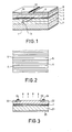
- Figure 1 shows, partly diagrammatically in cross-section and partly in perspective view, a semiconductor device according to the invention,
- Figure 2 shows diagrammatically in cross-section a detail of the device shown in Fig. 1, and
- Figure 3 shows diagrammatically in cross-section another semiconductor device according to the invention.
- The Figures are shown purely schematically and are not drawn to scale, while in particular the dimensions in the direction of thickness are strongly exaggerated.
- Corresponding parts are generally designated by the same reference numerals. Semiconductor regions of the same conductivity type are hatched in the same direction.
- Figure 1 shows, partly diagrammatically in cross-section and partly in perspective view, a semiconductor device for generating electromagnetic radiation according to the invention. The semiconductor device shown herein is a semiconductor laser and comprises an active layer-
shaped semiconductor region 1 lying between two semiconductor cladding layers 2 and 3 having a larger energy gap than the effective energy gap of theactive region 1. - The said
active region 1 is composed of a layer structure shown diagrammatically in cross-section in Figure 2. Figure 2shows apartofthe layer 1, which consists ofactive layers 4 of a first semiconductor material, in this example of undoped gallium arsenide, having approximately equal thicknesses. Theactive layers 4 lie between and are separated bybarrier layers 5 of a second semiconductor material, in this example of undoped aluminium arsenide, likewise having approximately equal thicknesses. The energy gap of aluminum arsenide is 2.30 eV, so larger than that of the gallium arsenide layers 4 (1.35 eV). Theactive layers 4 and thebarrier layers 5 together constitute a superlattice structure. - According to the invention, the
active layers 4 and also thebarrier layers 5 each comprise at least two and at most seven monolayers of the material of which these respective layers consist. In this example, theactive layers 4 have a thickness of 1.46 nm, which corresponds to six mono layers of GaAs. Thebarrier layers 5 in this example have a thickness of 0.97 nm, which corresponds to four layers of AlAs. The thickness of a GaAs monolayer is in fact 0.2444 nm and that of an AlAs mono-layer is 0.243 nm; see C. Hilsum and A.C. Rose-Innes, Semiconducting III-V Compounds, Pergamon Press, 1961, p. 6, Table 2.1. The total number of GaAs- and AlAs monolayers according to the invention does not exceed twelve, and in this example is 6+4=10. In this example, a total number of fourteenactive layers 4 and fifteenbarrier layers 5 are. These layers together constitute a superlattice of approximately 35 nm thickness. For radiation production the effective energy gap Eg of this superlattice is 1.95 eV. - This effective energy gap corresponds to a wave-length (in air or in a vacuum) of the generated radiation of 635 nm.
- The laser described in this example is, except for the
active region 1, entirely constructed as a conventional laser of the so-called double hetero-junction type. The layer-shapedregions 2, 1 and 3 are provided on an epitaxial layer 6 of n-type aluminum arsenide having a thickness of 2µm and a doping concentration of 2·1017 selenium atoms/cm3, which in turn is provided on a (100) orientatedsubstrate 7 of n-type gallium arsenide having a doping concentration of 2.1018 silicon atoms/cm3. The layer 2 is a layer of n-type aluminum arsenide having a thickness of 1.5µm and a doping concentration of 1018selenium atoms/cm3. The layer 3 is a p-type aluminum arsenide layer having a thickness of 1.5pm and a doping concentration of 2.10" zinc atoms/cm3. Finally, a further contact layer 8 of p-type gallium arsenide having a thickness of 1µm and a doping concentration of 2.1019 zinc atoms/cm3 is provided on the layer 3. - In order to form a strip-shaped active region in the
layer 1 in the operating condition, in the laser according to this example the layer 8 is coated with alayer 9 of silicon oxide, into which a strip-shapedaperture 12 is etched. Within this aperture anelectrode layer 10 is in contact with the layer 3. Anelectrode layer 11 is provided on the lower side of thesubstrate 7. - The crystal surfaces at right angles to the strip-shaped
aperture 12 are cleavage surfaces and serve as mirror surfaces for the laser. With a sufficiently high current between theanode 10 and thecathode 11, acoherent radiation beam 13 is generated having a wave-length of 635 nm. - The semiconductor layer shown in Figures 1 and 2 can be realized by means of different methods of epitaxial growth. The methods of "molecular beam epitaxy" (MBE) and of "metallo- organic chemical vapour deposition" (MOCVD) are particularly suitable. The former of these methods is described inter alia in United States Patent Specification 4,261,771 and the latter method in the article of Kasemset etal in Applied Physics Letters, Vol. 41, No. 10, November 15th 1982, p. 912-914. Thus. for example, with the use of the MBE technique, the following procedure may be applied.
- The starting member is an n-type
gallium arsenide substrate 7 having a doping concentration of 2.1018 silicon atoms/cm' and a (100) orientation. By means of known methods of epitaxial growth, an n-type AlAs layer 6 having a thickness of 2pm and a doping concentration of 2.1017 selenium atoms/cm3 and then an n-type layer 2 of AlAs having a doping concentration of 1018 selenium atoms/cm3 are grown on this substrate. Subsequently, the whole is placed in a chamber of an apparatus for MBE growth. At a substrate temperature of approximately 600°C and a pressure of approximately 0.133x10⁻⁸ kPa (10-8 Torr), 0.97 nmthick barrier layers 5 of undoped AlAs and 1.46 nm thickactive layers 4 of undoped GaAs are then grown alternately up to a total number of fifteenbarrier layers 5 and fourteenactive layers 4. Subsequently, a p-type layer 3 of AlAs having a thickness of 1.5 µm and a doping concentration of 2.10" zinc atoms/cm3 and a p-type GaAs layer 8 having a thickness of 1pm and a doping concentration of 2.1019 zinc atoms/cm3 are grown successively on this super- lattice structure. - Thereafter, an insulating
layer 9 of, for example, silicon oxide having a thickness of 0.1 µm is deposited on the surface of the layer 8. After strip-shapedwindows 12 have been etched into thisoxide layer 9, anelectrode layer 10 is deposited, after which the cleavage surfaces constituting the mirror surfaces of the lasers obtained are formed by scribing and breaking. Anelectrode layer 11 is deposited on thesubstrate 7 and the laser is provided on a heat sink with one of the electrode layers, preferably with theelectrode layer 10 located closest to theactive region 1, and is then finished in usual manner. - As has been stated already, the invention may also be used in light-emitting diodes. In the following example, such a diode will be described for generating non-coherent radiation having a wave-length of approximately 530 nm (green).
- Figure 3 shows diagrammatically in cross-section such a diode. The active layer-shaped
region 1 also in this case is a super lattice structure having a configuration as shown in Fig 2. In this case, however, theactive layers 4 consist of gallium phosphide (GaP), while the barrier layers 5 consist of aluminium phosphide (AIP). The number (n) of monolayers of the active GaP layers is four and the number (m) of the AIP barrier layers is also four. The thickness of a GaP mono- layer is 0.236 nm and the thickness of an AIP monolayer is also 0.236 nm. Also in this case, the conditions 2≤n≤7, 2≤m≤7 and n+m≤12 are satisfied. The energy gap of GaP is 2.25 eV and that of AIP is 2.5 eV. The effective energy gap of theactive region 1 is 2.34 eV. The total number ofactive layers 4 is fourteen and the total number of barrier layers is fifteen. The (green) light leaves the diode along the arrows via the part of the upper surface located within the annular electrode (anode) 24 with the associated annular p+-type contact zone 23. Theactive region 1 lies between a highly doped n-type substrate 21 of gallium phosphide and the p-type layer 22 of aluminium phosphide having a thickness of approximately 1µm and a doping concentration of approximately 10" zinc atoms/cm3. On the lower side of thesubstrate 21 is provided an electrode layer (cathode) 25. - The number of mono layers of which the
active layers 4 and the barrier layers 5 are composed, may be varied within the limits set thereto by the invention. The layer structure shown in Figure 1 may also be used as a source of non-coherent radiation in the absence of mirror surfaces. In the embodiments, the conductivity types of the various layers may be replaced (at the same time) by the opposite types. The wave-length of the generated radiation may then vary of course. Further, the total number of the active layers and barrier layers in the super lattice structure may be chosen larger or smaller than fifteen. Dependent upon the desired wave-length, both the aforementioned parameters n and m and the semiconductor materials of the various layers may be varied within the limits set by the invention and the technological possibilities. For example, instead of stoichiometric III-V compounds, stoichimetric II-VI compounds and/or elementary semiconductors, such as germanium, may be used.
Claims (6)
Applications Claiming Priority (2)
| Application Number | Priority Date | Filing Date | Title |
|---|---|---|---|
| NL8301215A NL8301215A (en) | 1983-04-07 | 1983-04-07 | SEMICONDUCTOR DEVICE FOR GENERATING ELECTROMAGNETIC RADIATION. |
| NL8301215 | 1983-04-07 |
Publications (2)
| Publication Number | Publication Date |
|---|---|
| EP0124924A1 EP0124924A1 (en) | 1984-11-14 |
| EP0124924B1 true EP0124924B1 (en) | 1987-09-02 |
Family
ID=19841666
Family Applications (1)
| Application Number | Title | Priority Date | Filing Date |
|---|---|---|---|
| EP84200473A Expired EP0124924B1 (en) | 1983-04-07 | 1984-04-04 | Semiconductor devise for generating electromagnetic radiation |
Country Status (5)
| Country | Link |
|---|---|
| US (1) | US4644378A (en) |
| EP (1) | EP0124924B1 (en) |
| JP (1) | JPS59197187A (en) |
| DE (1) | DE3465849D1 (en) |
| NL (1) | NL8301215A (en) |
Cited By (36)
| Publication number | Priority date | Publication date | Assignee | Title |
|---|---|---|---|---|
| US7926975B2 (en) | 2007-12-21 | 2011-04-19 | Altair Engineering, Inc. | Light distribution using a light emitting diode assembly |
| US7938562B2 (en) | 2008-10-24 | 2011-05-10 | Altair Engineering, Inc. | Lighting including integral communication apparatus |
| US7946729B2 (en) | 2008-07-31 | 2011-05-24 | Altair Engineering, Inc. | Fluorescent tube replacement having longitudinally oriented LEDs |
| US7976196B2 (en) | 2008-07-09 | 2011-07-12 | Altair Engineering, Inc. | Method of forming LED-based light and resulting LED-based light |
| US8118447B2 (en) | 2007-12-20 | 2012-02-21 | Altair Engineering, Inc. | LED lighting apparatus with swivel connection |
| US8214084B2 (en) | 2008-10-24 | 2012-07-03 | Ilumisys, Inc. | Integration of LED lighting with building controls |
| US8256924B2 (en) | 2008-09-15 | 2012-09-04 | Ilumisys, Inc. | LED-based light having rapidly oscillating LEDs |
| US8299695B2 (en) | 2009-06-02 | 2012-10-30 | Ilumisys, Inc. | Screw-in LED bulb comprising a base having outwardly projecting nodes |
| US8324817B2 (en) | 2008-10-24 | 2012-12-04 | Ilumisys, Inc. | Light and light sensor |
| US8330381B2 (en) | 2009-05-14 | 2012-12-11 | Ilumisys, Inc. | Electronic circuit for DC conversion of fluorescent lighting ballast |
| US8362710B2 (en) | 2009-01-21 | 2013-01-29 | Ilumisys, Inc. | Direct AC-to-DC converter for passive component minimization and universal operation of LED arrays |
| US8360599B2 (en) | 2008-05-23 | 2013-01-29 | Ilumisys, Inc. | Electric shock resistant L.E.D. based light |
| US8421366B2 (en) | 2009-06-23 | 2013-04-16 | Ilumisys, Inc. | Illumination device including LEDs and a switching power control system |
| US8444292B2 (en) | 2008-10-24 | 2013-05-21 | Ilumisys, Inc. | End cap substitute for LED-based tube replacement light |
| US8454193B2 (en) | 2010-07-08 | 2013-06-04 | Ilumisys, Inc. | Independent modules for LED fluorescent light tube replacement |
| US8523394B2 (en) | 2010-10-29 | 2013-09-03 | Ilumisys, Inc. | Mechanisms for reducing risk of shock during installation of light tube |
| US8541958B2 (en) | 2010-03-26 | 2013-09-24 | Ilumisys, Inc. | LED light with thermoelectric generator |
| US8540401B2 (en) | 2010-03-26 | 2013-09-24 | Ilumisys, Inc. | LED bulb with internal heat dissipating structures |
| US8556452B2 (en) | 2009-01-15 | 2013-10-15 | Ilumisys, Inc. | LED lens |
| US8596813B2 (en) | 2010-07-12 | 2013-12-03 | Ilumisys, Inc. | Circuit board mount for LED light tube |
| US8653984B2 (en) | 2008-10-24 | 2014-02-18 | Ilumisys, Inc. | Integration of LED lighting control with emergency notification systems |
| US8664880B2 (en) | 2009-01-21 | 2014-03-04 | Ilumisys, Inc. | Ballast/line detection circuit for fluorescent replacement lamps |
| US8674626B2 (en) | 2008-09-02 | 2014-03-18 | Ilumisys, Inc. | LED lamp failure alerting system |
| US8866396B2 (en) | 2000-02-11 | 2014-10-21 | Ilumisys, Inc. | Light tube and power supply circuit |
| US8870415B2 (en) | 2010-12-09 | 2014-10-28 | Ilumisys, Inc. | LED fluorescent tube replacement light with reduced shock hazard |
| US8901823B2 (en) | 2008-10-24 | 2014-12-02 | Ilumisys, Inc. | Light and light sensor |
| US9057493B2 (en) | 2010-03-26 | 2015-06-16 | Ilumisys, Inc. | LED light tube with dual sided light distribution |
| US9072171B2 (en) | 2011-08-24 | 2015-06-30 | Ilumisys, Inc. | Circuit board mount for LED light |
| US9163794B2 (en) | 2012-07-06 | 2015-10-20 | Ilumisys, Inc. | Power supply assembly for LED-based light tube |
| US9184518B2 (en) | 2012-03-02 | 2015-11-10 | Ilumisys, Inc. | Electrical connector header for an LED-based light |
| US9267650B2 (en) | 2013-10-09 | 2016-02-23 | Ilumisys, Inc. | Lens for an LED-based light |
| US9271367B2 (en) | 2012-07-09 | 2016-02-23 | Ilumisys, Inc. | System and method for controlling operation of an LED-based light |
| US9285084B2 (en) | 2013-03-14 | 2016-03-15 | Ilumisys, Inc. | Diffusers for LED-based lights |
| US9510400B2 (en) | 2014-05-13 | 2016-11-29 | Ilumisys, Inc. | User input systems for an LED-based light |
| US9574717B2 (en) | 2014-01-22 | 2017-02-21 | Ilumisys, Inc. | LED-based light with addressed LEDs |
| US10161568B2 (en) | 2015-06-01 | 2018-12-25 | Ilumisys, Inc. | LED-based light with canted outer walls |
Families Citing this family (27)
| Publication number | Priority date | Publication date | Assignee | Title |
|---|---|---|---|---|
| JPS6140082A (en) * | 1984-07-31 | 1986-02-26 | Sharp Corp | Semiconductor device |
| US5060234A (en) * | 1984-11-19 | 1991-10-22 | Max-Planck Gesellschaft Zur Forderung Der Wissenschaften | Injection laser with at least one pair of monoatomic layers of doping atoms |
| JPS61137383A (en) * | 1984-12-07 | 1986-06-25 | Sharp Corp | Photosemiconductor device |
| JPH0669109B2 (en) * | 1984-12-07 | 1994-08-31 | シャ−プ株式会社 | Optical semiconductor device |
| JPS61210679A (en) * | 1985-03-15 | 1986-09-18 | Sony Corp | Semiconductor device |
| JPS61220492A (en) * | 1985-03-27 | 1986-09-30 | Nec Corp | Quantum well laser |
| JPH0750795B2 (en) * | 1985-03-28 | 1995-05-31 | キヤノン株式会社 | Light emitting element |
| JPS61244086A (en) * | 1985-04-22 | 1986-10-30 | Sharp Corp | Semiconductor laser element |
| JPS6218082A (en) * | 1985-07-16 | 1987-01-27 | Sharp Corp | Semiconductor laser device |
| FR2589630B1 (en) * | 1985-07-23 | 1988-06-17 | Deveaud Benoit | SATURABLE ABSORBENT WITH VERY LOW SWITCHING TIMES |
| US4881235A (en) * | 1985-07-26 | 1989-11-14 | Hitachi, Ltd. | Semiconductor laser having a multiple quantum well structure doped with impurities |
| CA1279394C (en) * | 1985-07-26 | 1991-01-22 | Naoki Chinone | Multiple quantum well type semiconductor laser |
| JPS62165385A (en) * | 1986-01-14 | 1987-07-21 | Nec Corp | Semiconductor light emitting device |
| JPS62188295A (en) * | 1986-02-13 | 1987-08-17 | Sharp Corp | Semiconductor laser |
| JPS63153887A (en) * | 1986-08-08 | 1988-06-27 | Sharp Corp | Semiconductor laser device |
| JPS63207186A (en) * | 1987-02-24 | 1988-08-26 | Nippon Telegr & Teleph Corp <Ntt> | Material for visible-light region optical element |
| JP2544378B2 (en) * | 1987-03-25 | 1996-10-16 | 株式会社日立製作所 | Optical semiconductor device |
| ATE114386T1 (en) * | 1987-12-23 | 1994-12-15 | British Telecomm | SEMICONDUCTOR HETEROSSTRUCTURE. |
| CA1299719C (en) * | 1989-01-13 | 1992-04-28 | Hui Chun Liu | Semiconductor superlattice infrared source |
| JPH0327577A (en) * | 1989-06-23 | 1991-02-05 | イーストマン・コダックジャパン株式会社 | Light emitting diode array |
| DE69132934T2 (en) * | 1990-05-23 | 2002-08-29 | Uniphase Opto Holdings Inc | Radiation-emitting semiconductor device and method for producing the same |
| US5244749A (en) * | 1992-08-03 | 1993-09-14 | At&T Bell Laboratories | Article comprising an epitaxial multilayer mirror |
| US5362977A (en) * | 1992-12-28 | 1994-11-08 | At&T Bell Laboratories | Single mirror light-emitting diodes with enhanced intensity |
| US6603784B1 (en) * | 1998-12-21 | 2003-08-05 | Honeywell International Inc. | Mechanical stabilization of lattice mismatched quantum wells |
| US7860137B2 (en) * | 2004-10-01 | 2010-12-28 | Finisar Corporation | Vertical cavity surface emitting laser with undoped top mirror |
| CN101432936B (en) * | 2004-10-01 | 2011-02-02 | 菲尼萨公司 | Vertical cavity surface emitting laser having multiple top-side contacts |
| US20100309649A1 (en) * | 2009-06-09 | 2010-12-09 | Epistar Corporation | Photoelectronic device having a variable resistor structure |
Family Cites Families (6)
| Publication number | Priority date | Publication date | Assignee | Title |
|---|---|---|---|---|
| US3982207A (en) * | 1975-03-07 | 1976-09-21 | Bell Telephone Laboratories, Incorporated | Quantum effects in heterostructure lasers |
| US4205329A (en) * | 1976-03-29 | 1980-05-27 | Bell Telephone Laboratories, Incorporated | Periodic monolayer semiconductor structures grown by molecular beam epitaxy |
| US4261771A (en) * | 1979-10-31 | 1981-04-14 | Bell Telephone Laboratories, Incorporated | Method of fabricating periodic monolayer semiconductor structures by molecular beam epitaxy |
| US4439782A (en) * | 1980-11-21 | 1984-03-27 | University Of Illinois Foundation | Semiconductor device with heterojunction of Alx Ga1-x As--AlAs--Ga |
| JPS58500681A (en) * | 1981-05-06 | 1983-04-28 | ユニバ−シテイ オブ イリノイ フアンデ−シヨン | Manufacturing method of semiconductor device |
| JPS57187986A (en) * | 1981-05-15 | 1982-11-18 | Nippon Telegr & Teleph Corp <Ntt> | Semiconductor light emitting element |
-
1983
- 1983-04-07 NL NL8301215A patent/NL8301215A/en not_active Application Discontinuation
-
1984
- 1984-04-04 EP EP84200473A patent/EP0124924B1/en not_active Expired
- 1984-04-04 DE DE8484200473T patent/DE3465849D1/en not_active Expired
- 1984-04-06 JP JP59067779A patent/JPS59197187A/en active Granted
-
1985
- 1985-12-31 US US06/816,972 patent/US4644378A/en not_active Expired - Fee Related
Cited By (68)
| Publication number | Priority date | Publication date | Assignee | Title |
|---|---|---|---|---|
| US9752736B2 (en) | 2000-02-11 | 2017-09-05 | Ilumisys, Inc. | Light tube and power supply circuit |
| US9222626B1 (en) | 2000-02-11 | 2015-12-29 | Ilumisys, Inc. | Light tube and power supply circuit |
| US9746139B2 (en) | 2000-02-11 | 2017-08-29 | Ilumisys, Inc. | Light tube and power supply circuit |
| US8866396B2 (en) | 2000-02-11 | 2014-10-21 | Ilumisys, Inc. | Light tube and power supply circuit |
| US8870412B1 (en) | 2000-02-11 | 2014-10-28 | Ilumisys, Inc. | Light tube and power supply circuit |
| US9970601B2 (en) | 2000-02-11 | 2018-05-15 | Ilumisys, Inc. | Light tube and power supply circuit |
| US9803806B2 (en) | 2000-02-11 | 2017-10-31 | Ilumisys, Inc. | Light tube and power supply circuit |
| US9006990B1 (en) | 2000-02-11 | 2015-04-14 | Ilumisys, Inc. | Light tube and power supply circuit |
| US9777893B2 (en) | 2000-02-11 | 2017-10-03 | Ilumisys, Inc. | Light tube and power supply circuit |
| US9006993B1 (en) | 2000-02-11 | 2015-04-14 | Ilumisys, Inc. | Light tube and power supply circuit |
| US10054270B2 (en) | 2000-02-11 | 2018-08-21 | Ilumisys, Inc. | Light tube and power supply circuit |
| US9416923B1 (en) | 2000-02-11 | 2016-08-16 | Ilumisys, Inc. | Light tube and power supply circuit |
| US9759392B2 (en) | 2000-02-11 | 2017-09-12 | Ilumisys, Inc. | Light tube and power supply circuit |
| US9739428B1 (en) | 2000-02-11 | 2017-08-22 | Ilumisys, Inc. | Light tube and power supply circuit |
| US8928025B2 (en) | 2007-12-20 | 2015-01-06 | Ilumisys, Inc. | LED lighting apparatus with swivel connection |
| US8118447B2 (en) | 2007-12-20 | 2012-02-21 | Altair Engineering, Inc. | LED lighting apparatus with swivel connection |
| US7926975B2 (en) | 2007-12-21 | 2011-04-19 | Altair Engineering, Inc. | Light distribution using a light emitting diode assembly |
| US8807785B2 (en) | 2008-05-23 | 2014-08-19 | Ilumisys, Inc. | Electric shock resistant L.E.D. based light |
| US8360599B2 (en) | 2008-05-23 | 2013-01-29 | Ilumisys, Inc. | Electric shock resistant L.E.D. based light |
| US7976196B2 (en) | 2008-07-09 | 2011-07-12 | Altair Engineering, Inc. | Method of forming LED-based light and resulting LED-based light |
| US7946729B2 (en) | 2008-07-31 | 2011-05-24 | Altair Engineering, Inc. | Fluorescent tube replacement having longitudinally oriented LEDs |
| US8674626B2 (en) | 2008-09-02 | 2014-03-18 | Ilumisys, Inc. | LED lamp failure alerting system |
| US8256924B2 (en) | 2008-09-15 | 2012-09-04 | Ilumisys, Inc. | LED-based light having rapidly oscillating LEDs |
| US9635727B2 (en) | 2008-10-24 | 2017-04-25 | Ilumisys, Inc. | Light and light sensor |
| US8214084B2 (en) | 2008-10-24 | 2012-07-03 | Ilumisys, Inc. | Integration of LED lighting with building controls |
| US10342086B2 (en) | 2008-10-24 | 2019-07-02 | Ilumisys, Inc. | Integration of LED lighting with building controls |
| US8653984B2 (en) | 2008-10-24 | 2014-02-18 | Ilumisys, Inc. | Integration of LED lighting control with emergency notification systems |
| US10182480B2 (en) | 2008-10-24 | 2019-01-15 | Ilumisys, Inc. | Light and light sensor |
| US10176689B2 (en) | 2008-10-24 | 2019-01-08 | Ilumisys, Inc. | Integration of led lighting control with emergency notification systems |
| US7938562B2 (en) | 2008-10-24 | 2011-05-10 | Altair Engineering, Inc. | Lighting including integral communication apparatus |
| US8901823B2 (en) | 2008-10-24 | 2014-12-02 | Ilumisys, Inc. | Light and light sensor |
| US9353939B2 (en) | 2008-10-24 | 2016-05-31 | iLumisys, Inc | Lighting including integral communication apparatus |
| US8946996B2 (en) | 2008-10-24 | 2015-02-03 | Ilumisys, Inc. | Light and light sensor |
| US10036549B2 (en) | 2008-10-24 | 2018-07-31 | Ilumisys, Inc. | Lighting including integral communication apparatus |
| US9398661B2 (en) | 2008-10-24 | 2016-07-19 | Ilumisys, Inc. | Light and light sensor |
| US9585216B2 (en) | 2008-10-24 | 2017-02-28 | Ilumisys, Inc. | Integration of LED lighting with building controls |
| US8251544B2 (en) | 2008-10-24 | 2012-08-28 | Ilumisys, Inc. | Lighting including integral communication apparatus |
| US8444292B2 (en) | 2008-10-24 | 2013-05-21 | Ilumisys, Inc. | End cap substitute for LED-based tube replacement light |
| US9101026B2 (en) | 2008-10-24 | 2015-08-04 | Ilumisys, Inc. | Integration of LED lighting with building controls |
| US8324817B2 (en) | 2008-10-24 | 2012-12-04 | Ilumisys, Inc. | Light and light sensor |
| US8556452B2 (en) | 2009-01-15 | 2013-10-15 | Ilumisys, Inc. | LED lens |
| US8362710B2 (en) | 2009-01-21 | 2013-01-29 | Ilumisys, Inc. | Direct AC-to-DC converter for passive component minimization and universal operation of LED arrays |
| US8664880B2 (en) | 2009-01-21 | 2014-03-04 | Ilumisys, Inc. | Ballast/line detection circuit for fluorescent replacement lamps |
| US8330381B2 (en) | 2009-05-14 | 2012-12-11 | Ilumisys, Inc. | Electronic circuit for DC conversion of fluorescent lighting ballast |
| US8299695B2 (en) | 2009-06-02 | 2012-10-30 | Ilumisys, Inc. | Screw-in LED bulb comprising a base having outwardly projecting nodes |
| US8421366B2 (en) | 2009-06-23 | 2013-04-16 | Ilumisys, Inc. | Illumination device including LEDs and a switching power control system |
| US9013119B2 (en) | 2010-03-26 | 2015-04-21 | Ilumisys, Inc. | LED light with thermoelectric generator |
| US9395075B2 (en) | 2010-03-26 | 2016-07-19 | Ilumisys, Inc. | LED bulb for incandescent bulb replacement with internal heat dissipating structures |
| US8840282B2 (en) | 2010-03-26 | 2014-09-23 | Ilumisys, Inc. | LED bulb with internal heat dissipating structures |
| US8540401B2 (en) | 2010-03-26 | 2013-09-24 | Ilumisys, Inc. | LED bulb with internal heat dissipating structures |
| US8541958B2 (en) | 2010-03-26 | 2013-09-24 | Ilumisys, Inc. | LED light with thermoelectric generator |
| US9057493B2 (en) | 2010-03-26 | 2015-06-16 | Ilumisys, Inc. | LED light tube with dual sided light distribution |
| US8454193B2 (en) | 2010-07-08 | 2013-06-04 | Ilumisys, Inc. | Independent modules for LED fluorescent light tube replacement |
| US8596813B2 (en) | 2010-07-12 | 2013-12-03 | Ilumisys, Inc. | Circuit board mount for LED light tube |
| US8894430B2 (en) | 2010-10-29 | 2014-11-25 | Ilumisys, Inc. | Mechanisms for reducing risk of shock during installation of light tube |
| US8523394B2 (en) | 2010-10-29 | 2013-09-03 | Ilumisys, Inc. | Mechanisms for reducing risk of shock during installation of light tube |
| US8870415B2 (en) | 2010-12-09 | 2014-10-28 | Ilumisys, Inc. | LED fluorescent tube replacement light with reduced shock hazard |
| US9072171B2 (en) | 2011-08-24 | 2015-06-30 | Ilumisys, Inc. | Circuit board mount for LED light |
| US9184518B2 (en) | 2012-03-02 | 2015-11-10 | Ilumisys, Inc. | Electrical connector header for an LED-based light |
| US9163794B2 (en) | 2012-07-06 | 2015-10-20 | Ilumisys, Inc. | Power supply assembly for LED-based light tube |
| US9807842B2 (en) | 2012-07-09 | 2017-10-31 | Ilumisys, Inc. | System and method for controlling operation of an LED-based light |
| US9271367B2 (en) | 2012-07-09 | 2016-02-23 | Ilumisys, Inc. | System and method for controlling operation of an LED-based light |
| US9285084B2 (en) | 2013-03-14 | 2016-03-15 | Ilumisys, Inc. | Diffusers for LED-based lights |
| US9267650B2 (en) | 2013-10-09 | 2016-02-23 | Ilumisys, Inc. | Lens for an LED-based light |
| US9574717B2 (en) | 2014-01-22 | 2017-02-21 | Ilumisys, Inc. | LED-based light with addressed LEDs |
| US10260686B2 (en) | 2014-01-22 | 2019-04-16 | Ilumisys, Inc. | LED-based light with addressed LEDs |
| US9510400B2 (en) | 2014-05-13 | 2016-11-29 | Ilumisys, Inc. | User input systems for an LED-based light |
| US10161568B2 (en) | 2015-06-01 | 2018-12-25 | Ilumisys, Inc. | LED-based light with canted outer walls |
Also Published As
| Publication number | Publication date |
|---|---|
| NL8301215A (en) | 1984-11-01 |
| EP0124924A1 (en) | 1984-11-14 |
| US4644378A (en) | 1987-02-17 |
| JPH048956B2 (en) | 1992-02-18 |
| JPS59197187A (en) | 1984-11-08 |
| DE3465849D1 (en) | 1987-10-08 |
Similar Documents
| Publication | Publication Date | Title |
|---|---|---|
| EP0124924B1 (en) | Semiconductor devise for generating electromagnetic radiation | |
| US5838029A (en) | GaN-type light emitting device formed on a silicon substrate | |
| JP3425185B2 (en) | Semiconductor element | |
| US5937274A (en) | Fabrication method for AlGaIn NPAsSb based devices | |
| JP3672678B2 (en) | Quantum semiconductor device and manufacturing method thereof | |
| US6525335B1 (en) | Light emitting semiconductor devices including wafer bonded heterostructures | |
| US4439782A (en) | Semiconductor device with heterojunction of Alx Ga1-x As--AlAs--Ga | |
| EP0378919B1 (en) | High band-gap opto-electronic device and method for making same | |
| JPH0418476B2 (en) | ||
| KR910003465B1 (en) | Opto-electronic device | |
| US5687185A (en) | Laser cathode-ray tube | |
| US4365260A (en) | Semiconductor light emitting device with quantum well active region of indirect bandgap semiconductor material | |
| US5331656A (en) | Very short wavelength semiconductor laser | |
| US5812574A (en) | Quantum optical semiconductor device producing output optical emission with sharply defined spectrum | |
| US6081001A (en) | Nitride semiconductor light emitting device | |
| EP0188080B1 (en) | Light-emitting semiconductor device having a super lattice | |
| JP2969979B2 (en) | Semiconductor structures for optoelectronic components | |
| WO2001009996A1 (en) | Semiconductor structures using a group iii-nitride quaternary material system | |
| US4270094A (en) | Semiconductor light emitting device | |
| US5057881A (en) | Light emitting compositional semiconductor device | |
| GB2137812A (en) | Semiconductor Device for Producing Electromagnetic Radiation | |
| JP3364970B2 (en) | Polarized electron beam generator | |
| JPH05343796A (en) | Surface emission-type semiconductor laser | |
| Windhorn et al. | GaAs/AlGaAs diode lasers on monolithic GaAs/Si substrates | |
| JP2825957B2 (en) | Semiconductor light receiving element |
Legal Events
| Date | Code | Title | Description |
|---|---|---|---|
| PUAI | Public reference made under article 153(3) epc to a published international application that has entered the european phase |
Free format text: ORIGINAL CODE: 0009012 |
|
| AK | Designated contracting states |
Designated state(s): DE FR GB NL |
|
| 17P | Request for examination filed |
Effective date: 19841130 |
|
| 17Q | First examination report despatched |
Effective date: 19860224 |
|
| GRAA | (expected) grant |
Free format text: ORIGINAL CODE: 0009210 |
|
| AK | Designated contracting states |
Kind code of ref document: B1 Designated state(s): DE FR GB NL |
|
| REF | Corresponds to: |
Ref document number: 3465849 Country of ref document: DE Date of ref document: 19871008 |
|
| ET | Fr: translation filed | ||
| PLBE | No opposition filed within time limit |
Free format text: ORIGINAL CODE: 0009261 |
|
| STAA | Information on the status of an ep patent application or granted ep patent |
Free format text: STATUS: NO OPPOSITION FILED WITHIN TIME LIMIT |
|
| 26N | No opposition filed | ||
| PGFP | Annual fee paid to national office [announced via postgrant information from national office to epo] |
Ref country code: NL Payment date: 19900430 Year of fee payment: 7 |
|
| PG25 | Lapsed in a contracting state [announced via postgrant information from national office to epo] |
Ref country code: NL Effective date: 19911101 |
|
| NLV4 | Nl: lapsed or anulled due to non-payment of the annual fee | ||
| REG | Reference to a national code |
Ref country code: FR Ref legal event code: CD |
|
| PGFP | Annual fee paid to national office [announced via postgrant information from national office to epo] |
Ref country code: GB Payment date: 19960329 Year of fee payment: 13 |
|
| PGFP | Annual fee paid to national office [announced via postgrant information from national office to epo] |
Ref country code: FR Payment date: 19960429 Year of fee payment: 13 |
|
| PGFP | Annual fee paid to national office [announced via postgrant information from national office to epo] |
Ref country code: DE Payment date: 19960625 Year of fee payment: 13 |
|
| PG25 | Lapsed in a contracting state [announced via postgrant information from national office to epo] |
Ref country code: GB Effective date: 19970404 |
|
| GBPC | Gb: european patent ceased through non-payment of renewal fee |
Effective date: 19970404 |
|
| PG25 | Lapsed in a contracting state [announced via postgrant information from national office to epo] |
Ref country code: FR Free format text: LAPSE BECAUSE OF NON-PAYMENT OF DUE FEES Effective date: 19971231 |
|
| PG25 | Lapsed in a contracting state [announced via postgrant information from national office to epo] |
Ref country code: DE Free format text: LAPSE BECAUSE OF NON-PAYMENT OF DUE FEES Effective date: 19980101 |
|
| REG | Reference to a national code |
Ref country code: FR Ref legal event code: ST |