EP0127743A2 - Light detecting circuit - Google Patents
Light detecting circuit Download PDFInfo
- Publication number
- EP0127743A2 EP0127743A2 EP84103653A EP84103653A EP0127743A2 EP 0127743 A2 EP0127743 A2 EP 0127743A2 EP 84103653 A EP84103653 A EP 84103653A EP 84103653 A EP84103653 A EP 84103653A EP 0127743 A2 EP0127743 A2 EP 0127743A2
- Authority
- EP
- European Patent Office
- Prior art keywords
- photodiode
- light detecting
- detecting circuit
- input terminal
- bias voltage
- Prior art date
- Legal status (The legal status is an assumption and is not a legal conclusion. Google has not performed a legal analysis and makes no representation as to the accuracy of the status listed.)
- Withdrawn
Links
- 230000003071 parasitic effect Effects 0.000 claims abstract description 14
- 239000003990 capacitor Substances 0.000 claims abstract description 12
- 230000003287 optical effect Effects 0.000 claims description 8
- 230000002411 adverse Effects 0.000 description 2
- 238000010586 diagram Methods 0.000 description 2
- 230000035945 sensitivity Effects 0.000 description 2
- 230000003247 decreasing effect Effects 0.000 description 1
- 238000001514 detection method Methods 0.000 description 1
- 238000004519 manufacturing process Methods 0.000 description 1
Images

Classifications
-
- H—ELECTRICITY
- H03—ELECTRONIC CIRCUITRY
- H03F—AMPLIFIERS
- H03F3/00—Amplifiers with only discharge tubes or only semiconductor devices as amplifying elements
- H03F3/04—Amplifiers with only discharge tubes or only semiconductor devices as amplifying elements with semiconductor devices only
- H03F3/08—Amplifiers with only discharge tubes or only semiconductor devices as amplifying elements with semiconductor devices only controlled by light
- H03F3/087—Amplifiers with only discharge tubes or only semiconductor devices as amplifying elements with semiconductor devices only controlled by light with IC amplifier blocks
-
- G—PHYSICS
- G01—MEASURING; TESTING
- G01J—MEASUREMENT OF INTENSITY, VELOCITY, SPECTRAL CONTENT, POLARISATION, PHASE OR PULSE CHARACTERISTICS OF INFRARED, VISIBLE OR ULTRAVIOLET LIGHT; COLORIMETRY; RADIATION PYROMETRY
- G01J1/00—Photometry, e.g. photographic exposure meter
- G01J1/42—Photometry, e.g. photographic exposure meter using electric radiation detectors
- G01J1/44—Electric circuits
-
- H—ELECTRICITY
- H04—ELECTRIC COMMUNICATION TECHNIQUE
- H04B—TRANSMISSION
- H04B10/00—Transmission systems employing electromagnetic waves other than radio-waves, e.g. infrared, visible or ultraviolet light, or employing corpuscular radiation, e.g. quantum communication
- H04B10/60—Receivers
- H04B10/66—Non-coherent receivers, e.g. using direct detection
- H04B10/69—Electrical arrangements in the receiver
- H04B10/691—Arrangements for optimizing the photodetector in the receiver
- H04B10/6911—Photodiode bias control, e.g. for compensating temperature variations
Definitions
- the present invention relates to a light detecting circuit which can cancel or suppress a noise component superposed on a bias voltage which might otherwise adversely affect the detected light signal.
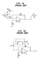
- Figs. 1A and lB shows conventional light detecting circuits.
- reference numeral 1 designates a light detecting photodiode; 2, a differential amplifier; and 3, a noise filter.
- V b bias voltage
- V b bias voltage
- the noise is applied to an input terminal of the differential amplifier 2 through a parasitic capacitor Ct, typically about 3 pF, of the photodiode 1 and is amplified together with the received optical signal by the differential amplifier 2.
- Such noise adversely affects the detection of the optical signal received by the photodiode 1. For instance, if the noise voltage is 10 mV and the parasitic capacitor Ct of the photodiode is 3 pF, the noise current flowing through the parasitic capacitor Ct is about 1.8 pA. If the optical input has a power level of 1 ⁇ W, the corresponding signal current is 0.6 pA. Therefore, it can be understood that the noise current is much larger than the signal current. Accordingly, in the conventional light detecting circuit, it is necessary to apply the bias voltage V b through the noise filter 3 which is used for a bias circuit, as shown in Fig. 1B. However, the circuit indicated in Fig. 1B is disadvantageous in that it is space consuming, particularly, in that the inductor required thereby cannot be readily fabricated in integrated circuit form.
- the invention provides a light detecting circuit including a first photodiode for receiving an optical signal and converting the optical signal into an electrical signal with the first photodiode being coupled to a bias voltage source, a main amplifier receiving the electrical signal on one of two input terminals thereof for amplifying the electrical signal, and capacitance means coupled to the other terminal of the main amplifier and to the bias voltage source for cancelling a noise -component mixed in the circuit, due to the parasitic capacitance of the first photodiode, from the bias voltage terminal.
- the main amplifier may be a differential amplifier or a comparator, and the two input terminals the inverting and noninverting terminals thereof, respectively.
- the capacitance means may be a capacitor having a capacitance value equal to the parasitic capacitance of the first photodiode, or a second photodiode having a parasitic capacitance equal to that of the first photodiode.
- Fig. 2 shows a first example of a light detecting circuit constructed according to the invention.
- a capacitor C l which is substantially equal in capacitance value to the parasitic capacitance Ct of the photodiode 1, is connected between the bias voltage V b terminal and the -noninverting input terminal of the differential amplifier 2. Therefore, a noise component mixed in the bias voltage V b applied through the parasitic capacitance Ct of the photodiode 1 to the inverting input terminal of the differential amplifier 2 is also applied through the capacitor C l to the noninverting input terminal of the differential amplifier 2.
- the common mode rejection ratio (CMMR) of the differential amplifier 2 is ideal and the capacitance value of the capacitor C l is equal to that C t of the photodiode, the noise superposed on the bias voltage V b is not outputted by the differential amplifier 2 since it is completely canceled out.
- the common mode rejection ratio of the differential amplifier 2 is of the order of 80 dB in the DC region, but in the high frequency region it is often of the order of 20 dB (at 10 MHz). Therefore, although complete cancellation is not effected in the high frequency region, the noise can be suppressed by 20 dB, that is, to one-tenth of the original level.
- a noise current of 1.8 pA as mentioned above can be reduced to 0.18 ⁇ A.
- the signal detecting sensitivity of the circuit can be markedly increased. That is, in order to successfully detect a signal, the signal -voltage must be much larger than the noise voltage, and in the light detecting circuit of the invention the value of the necessary signal voltage can be reduced by an order of magnitude. This means that the signal detecting sensitivity can be increased by an order of magnitude. If it is assumed, for instance, that the load resistance is 50 K ⁇ , and if the noise current is 1.8 ⁇ A as mentioned above, the noise voltage is 90 mV in the conventional light detecting circuit, but it is 9 mV in the light detecting circuit of the invention.
- Fig. 3 shows a second example of a light detecting circuit of the invention.
- a comparator 4 is employed as a main amplifier.
- a capacitor C l is connected to the input terminal of a photodiode 1 to cancel or suppress noise mixed in the bias voltage V b .
- Fig. 4 shows a third example of a light detecting circuit of the invention.
- a dummy photodiode 1' is provided in parallel with the photodiode 1, and the photodiode 1' is arranged so as to not receive an optical signal. If the dummy photodiode l' has the same characteristics as the photodiode 1, that is, if the parasitic capacitance of the former is equal to that of the latter, noise mixed in the bias voltage V b can be completely canceled out.
- the output characteristic of the arrangement of Fig. 4 is preferred over that of the arrangement of Fig. 2 or 3 in which the capacitor C l is employed. However, the system using the capacitor C 1 is advantageous with respect to manufacturing cost and the utilization of space.
Abstract
Description
- The present invention relates to a light detecting circuit which can cancel or suppress a noise component superposed on a bias voltage which might otherwise adversely affect the detected light signal.
- Figs. 1A and lB shows conventional light detecting circuits. In these figures, reference numeral 1 designates a light detecting photodiode; 2, a differential amplifier; and 3, a noise filter. In order to operate the light detecting photodiode 1, it is necessary to apply a bias voltage Vb thereto; however, when the light detecting photodiode 1 is operated, a noise component having a waveform as shown at the top of Fig. lA is often superposed on the bias voltage Vb. The noise is applied to an input terminal of the
differential amplifier 2 through a parasitic capacitor Ct, typically about 3 pF, of the photodiode 1 and is amplified together with the received optical signal by thedifferential amplifier 2. - Such noise adversely affects the detection of the optical signal received by the photodiode 1. For instance, if the noise voltage is 10 mV and the parasitic capacitor Ct of the photodiode is 3 pF, the noise current flowing through the parasitic capacitor Ct is about 1.8 pA. If the optical input has a power level of 1 µW, the corresponding signal current is 0.6 pA. Therefore, it can be understood that the noise current is much larger than the signal current. Accordingly, in the conventional light detecting circuit, it is necessary to apply the bias voltage Vb through the
noise filter 3 which is used for a bias circuit, as shown in Fig. 1B. However, the circuit indicated in Fig. 1B is disadvantageous in that it is space consuming, particularly, in that the inductor required thereby cannot be readily fabricated in integrated circuit form. - Accordingly, it is an object of the present invention to provide a light detecting circuit in which a noise component superposed on a bias voltage is eliminated without the use of a filter circuit.
- In accordance with the above and other objects, the invention provides a light detecting circuit including a first photodiode for receiving an optical signal and converting the optical signal into an electrical signal with the first photodiode being coupled to a bias voltage source, a main amplifier receiving the electrical signal on one of two input terminals thereof for amplifying the electrical signal, and capacitance means coupled to the other terminal of the main amplifier and to the bias voltage source for cancelling a noise -component mixed in the circuit, due to the parasitic capacitance of the first photodiode, from the bias voltage terminal. The main amplifier may be a differential amplifier or a comparator, and the two input terminals the inverting and noninverting terminals thereof, respectively. The capacitance means may be a capacitor having a capacitance value equal to the parasitic capacitance of the first photodiode, or a second photodiode having a parasitic capacitance equal to that of the first photodiode.
-
- Figs. lA and lB are circuit diagrams showing conventional light detecting circuits; and
- Figs. 2, 3 and 4 are circuit diagrams of first, second and third examples of a light detecting circuit according to the invention.
- Preferred embodiments of the invention will be described in detail with reference to Figs. 2, 3 and 4.
- Fig. 2 shows a first example of a light detecting circuit constructed according to the invention. In this example, a capacitor Cl, which is substantially equal in capacitance value to the parasitic capacitance Ct of the photodiode 1, is connected between the bias voltage Vb terminal and the -noninverting input terminal of the
differential amplifier 2. Therefore, a noise component mixed in the bias voltage Vb applied through the parasitic capacitance Ct of the photodiode 1 to the inverting input terminal of thedifferential amplifier 2 is also applied through the capacitor Cl to the noninverting input terminal of thedifferential amplifier 2. Accordingly, if the common mode rejection ratio (CMMR) of thedifferential amplifier 2 is ideal and the capacitance value of the capacitor Cl is equal to that Ct of the photodiode, the noise superposed on the bias voltage Vb is not outputted by thedifferential amplifier 2 since it is completely canceled out. In practice, the common mode rejection ratio of thedifferential amplifier 2 is of the order of 80 dB in the DC region, but in the high frequency region it is often of the order of 20 dB (at 10 MHz). Therefore, although complete cancellation is not effected in the high frequency region, the noise can be suppressed by 20 dB, that is, to one-tenth of the original level. Thus, a noise current of 1.8 pA as mentioned above can be reduced to 0.18 µA. - As the noise current is greatly decreased according to the invention as described above, the signal detecting sensitivity of the circuit can be markedly increased. That is, in order to successfully detect a signal, the signal -voltage must be much larger than the noise voltage, and in the light detecting circuit of the invention the value of the necessary signal voltage can be reduced by an order of magnitude. This means that the signal detecting sensitivity can be increased by an order of magnitude. If it is assumed, for instance, that the load resistance is 50 KΩ, and if the noise current is 1.8 µA as mentioned above, the noise voltage is 90 mV in the conventional light detecting circuit, but it is 9 mV in the light detecting circuit of the invention.
- Fig. 3 shows a second example of a light detecting circuit of the invention. In this example, instead of the
differential amplifier 2, acomparator 4 is employed as a main amplifier. In this example as well, a capacitor Cl is connected to the input terminal of a photodiode 1 to cancel or suppress noise mixed in the bias voltage Vb. - Fig. 4 shows a third example of a light detecting circuit of the invention. In the third example, a dummy photodiode 1' is provided in parallel with the photodiode 1, and the photodiode 1' is arranged so as to not receive an optical signal. If the dummy photodiode l' has the same characteristics as the photodiode 1, that is, if the parasitic capacitance of the former is equal to that of the latter, noise mixed in the bias voltage Vb can be completely canceled out. The output characteristic of the arrangement of Fig. 4 is preferred over that of the arrangement of Fig. 2 or 3 in which the capacitor Cl is employed. However, the system using the capacitor C1 is advantageous with respect to manufacturing cost and the utilization of space.
Claims (7)
Applications Claiming Priority (2)
| Application Number | Priority Date | Filing Date | Title |
|---|---|---|---|
| JP59816/83 | 1983-04-05 | ||
| JP58059816A JPS59185432A (en) | 1983-04-05 | 1983-04-05 | Optical receiving circuit |
Publications (2)
| Publication Number | Publication Date |
|---|---|
| EP0127743A2 true EP0127743A2 (en) | 1984-12-12 |
| EP0127743A3 EP0127743A3 (en) | 1987-02-25 |
Family
ID=13124126
Family Applications (1)
| Application Number | Title | Priority Date | Filing Date |
|---|---|---|---|
| EP84103653A Withdrawn EP0127743A3 (en) | 1983-04-05 | 1984-04-03 | Light detecting circuit |
Country Status (5)
| Country | Link |
|---|---|
| US (1) | US4626678A (en) |
| EP (1) | EP0127743A3 (en) |
| JP (1) | JPS59185432A (en) |
| CA (1) | CA1223938A (en) |
| DK (1) | DK178684A (en) |
Cited By (2)
| Publication number | Priority date | Publication date | Assignee | Title |
|---|---|---|---|---|
| US6751583B1 (en) | 1999-10-29 | 2004-06-15 | Vast Systems Technology Corporation | Hardware and software co-simulation including simulating a target processor using binary translation |
| DE102014103770B4 (en) | 2013-03-26 | 2018-10-31 | Excelitas Canada Inc. | Optical differential amplifier for avalanche photodiodes and SiPM |
Families Citing this family (12)
| Publication number | Priority date | Publication date | Assignee | Title |
|---|---|---|---|---|
| JPH0732261B2 (en) * | 1985-04-11 | 1995-04-10 | キヤノン株式会社 | Semiconductor light receiving device |
| US4819646A (en) * | 1986-08-18 | 1989-04-11 | Physio-Control Corporation | Feedback-controlled method and apparatus for processing signals used in oximetry |
| US4913150A (en) * | 1986-08-18 | 1990-04-03 | Physio-Control Corporation | Method and apparatus for the automatic calibration of signals employed in oximetry |
| US8352400B2 (en) | 1991-12-23 | 2013-01-08 | Hoffberg Steven M | Adaptive pattern recognition based controller apparatus and method and human-factored interface therefore |
| US10361802B1 (en) | 1999-02-01 | 2019-07-23 | Blanding Hovenweep, Llc | Adaptive pattern recognition based control system and method |
| US5479044A (en) * | 1993-06-25 | 1995-12-26 | Nec Corporation | Semiconductor circuit device capable of reducing influence of a parasitic capacitor |
| US5504456A (en) * | 1994-02-09 | 1996-04-02 | Psc, Inc. | Low noise wide band amplifier |
| JP3680303B2 (en) * | 1994-11-08 | 2005-08-10 | 住友電気工業株式会社 | Photoelectric conversion module |
| US5763873A (en) * | 1996-08-28 | 1998-06-09 | Patchen, Inc. | Photodetector circuit for an electronic sprayer |
| US7966078B2 (en) | 1999-02-01 | 2011-06-21 | Steven Hoffberg | Network media appliance system and method |
| JP4187376B2 (en) * | 2000-02-16 | 2008-11-26 | ローム株式会社 | Photoreceiver / amplifier |
| JP4611255B2 (en) * | 2006-07-18 | 2011-01-12 | ルネサスエレクトロニクス株式会社 | Semiconductor photo detector |
Citations (1)
| Publication number | Priority date | Publication date | Assignee | Title |
|---|---|---|---|---|
| US3978343A (en) * | 1975-06-30 | 1976-08-31 | National Semiconductor Corporation | Optically coupled isolator circuit having increased common mode rejection |
Family Cites Families (2)
| Publication number | Priority date | Publication date | Assignee | Title |
|---|---|---|---|---|
| CA1024239A (en) * | 1972-04-17 | 1978-01-10 | Rca Limited | Low noise detector amplifier |
| JPS57207445A (en) * | 1981-06-17 | 1982-12-20 | Hitachi Ltd | Environmental noise compensating system for optical receiver |
-
1983
- 1983-04-05 JP JP58059816A patent/JPS59185432A/en active Pending
-
1984
- 1984-04-03 EP EP84103653A patent/EP0127743A3/en not_active Withdrawn
- 1984-04-04 DK DK178684A patent/DK178684A/en not_active Application Discontinuation
- 1984-04-04 US US06/596,751 patent/US4626678A/en not_active Expired - Lifetime
- 1984-04-04 CA CA000451249A patent/CA1223938A/en not_active Expired
Patent Citations (1)
| Publication number | Priority date | Publication date | Assignee | Title |
|---|---|---|---|---|
| US3978343A (en) * | 1975-06-30 | 1976-08-31 | National Semiconductor Corporation | Optically coupled isolator circuit having increased common mode rejection |
Non-Patent Citations (2)
| Title |
|---|
| ELEKTRONIK, vol. 21, no. 5, May 1972, page 160; H. GUENTNER et al.: "Temperaturkompensierter Fotoempfaenger" * |
| PATENT ABSTRACTS OF JAPAN, vol. 7, no. 72 (E-166)[1217], 25th March 1983; & JP 58003335 A (SUMITOMO DENKI KOGYO K.K.) 10-01-1983 * |
Cited By (2)
| Publication number | Priority date | Publication date | Assignee | Title |
|---|---|---|---|---|
| US6751583B1 (en) | 1999-10-29 | 2004-06-15 | Vast Systems Technology Corporation | Hardware and software co-simulation including simulating a target processor using binary translation |
| DE102014103770B4 (en) | 2013-03-26 | 2018-10-31 | Excelitas Canada Inc. | Optical differential amplifier for avalanche photodiodes and SiPM |
Also Published As
| Publication number | Publication date |
|---|---|
| JPS59185432A (en) | 1984-10-22 |
| DK178684A (en) | 1984-10-06 |
| CA1223938A (en) | 1987-07-07 |
| DK178684D0 (en) | 1984-04-04 |
| EP0127743A3 (en) | 1987-02-25 |
| US4626678A (en) | 1986-12-02 |
Similar Documents
| Publication | Publication Date | Title |
|---|---|---|
| US4626678A (en) | Light detecting circuit | |
| US5491434A (en) | Circuit and method of differential amplitude detection | |
| KR910009088B1 (en) | Radio frequency detector | |
| US6476660B1 (en) | Fully integrated long time constant integrator circuit | |
| US5371479A (en) | Pre-amplifier with multi-stage feedback | |
| US4613769A (en) | Direct current coupled peak to peak detector circuit | |
| GB2198307A (en) | Avoiding d.c. offsets and crossover distortion in voltage-to-current converters | |
| US4975566A (en) | First stage circuit for an optical receiver | |
| US20050175359A1 (en) | Optical receiver | |
| US6552615B1 (en) | Method and system for compensation of low-frequency photodiode current in a transimpedance amplifier | |
| US4303889A (en) | Filter circuit | |
| US5212378A (en) | Optical receiver with critical damping resistor | |
| US5592155A (en) | Remote control infrared receiver with light detector and pre-amplifier | |
| US4654603A (en) | Low input-capacitance amplifier for driving guard shield conductors | |
| US2974288A (en) | D.-c. amplifier and filter therefor | |
| JPH0793540B2 (en) | Optical receiver | |
| EP0460273A1 (en) | Gain stabilizing amplifier | |
| JP3179838B2 (en) | Noise detection circuit | |
| US5104223A (en) | Optical interferometric sensor detected intensity noise reduction means | |
| GB2194406A (en) | Optical signal receiver circuits | |
| JP2597482Y2 (en) | Photoelectric switch | |
| JPS6042539Y2 (en) | Laser light receiving circuit | |
| JPH02164112A (en) | Optical receiver | |
| JPH10274665A (en) | Current detector | |
| JPH04259105A (en) | Amplifier circuit |
Legal Events
| Date | Code | Title | Description |
|---|---|---|---|
| PUAI | Public reference made under article 153(3) epc to a published international application that has entered the european phase |
Free format text: ORIGINAL CODE: 0009012 |
|
| AK | Designated contracting states |
Designated state(s): DE FR GB IT SE |
|
| PUAL | Search report despatched |
Free format text: ORIGINAL CODE: 0009013 |
|
| AK | Designated contracting states |
Kind code of ref document: A3 Designated state(s): DE FR GB IT SE |
|
| RAP1 | Party data changed (applicant data changed or rights of an application transferred) |
Owner name: SUMITOMO ELECTRIC INDUSTRIES LIMITED |
|
| 17P | Request for examination filed |
Effective date: 19870410 |
|
| 17Q | First examination report despatched |
Effective date: 19881018 |
|
| STAA | Information on the status of an ep patent application or granted ep patent |
Free format text: STATUS: THE APPLICATION IS DEEMED TO BE WITHDRAWN |
|
| 18D | Application deemed to be withdrawn |
Effective date: 19900112 |
|
| RIN1 | Information on inventor provided before grant (corrected) |
Inventor name: NISHIE, MITSUAKIC/O YOKOHAMA WORKS Inventor name: MORITA, TETSUOC/O YOKOHAMA WORKS |