EP0128559A2 - A load cell type weight measuring device and a sensitivity checking method thereof - Google Patents
A load cell type weight measuring device and a sensitivity checking method thereof Download PDFInfo
- Publication number
- EP0128559A2 EP0128559A2 EP84106584A EP84106584A EP0128559A2 EP 0128559 A2 EP0128559 A2 EP 0128559A2 EP 84106584 A EP84106584 A EP 84106584A EP 84106584 A EP84106584 A EP 84106584A EP 0128559 A2 EP0128559 A2 EP 0128559A2
- Authority
- EP
- European Patent Office
- Prior art keywords
- load cell
- output voltage
- voltage
- amplifier
- measuring device
- Prior art date
- Legal status (The legal status is an assumption and is not a legal conclusion. Google has not performed a legal analysis and makes no representation as to the accuracy of the status listed.)
- Granted
Links
Images


Classifications
-
- G—PHYSICS
- G01—MEASURING; TESTING
- G01G—WEIGHING
- G01G23/00—Auxiliary devices for weighing apparatus
- G01G23/01—Testing or calibrating of weighing apparatus
-
- G—PHYSICS
- G01—MEASURING; TESTING
- G01G—WEIGHING
- G01G3/00—Weighing apparatus characterised by the use of elastically-deformable members, e.g. spring balances
- G01G3/12—Weighing apparatus characterised by the use of elastically-deformable members, e.g. spring balances wherein the weighing element is in the form of a solid body stressed by pressure or tension during weighing
- G01G3/14—Weighing apparatus characterised by the use of elastically-deformable members, e.g. spring balances wherein the weighing element is in the form of a solid body stressed by pressure or tension during weighing measuring variations of electrical resistance
- G01G3/142—Circuits specially adapted therefor
- G01G3/147—Circuits specially adapted therefor involving digital counting
Definitions
- the present invention relates to a load cell type weight measuring device and a sensitivity checking method thereof.
- Another object of the invention is to provide a sensitivity checking method in the load cell type weight measuring device.
- a load cell type weight measuring device comprising a load cell producing an output voltage corresponding to the weight applied thereto; a rated voltage generating circuit for generating an output voltage equal to the output voltage generated by this load cell which is applied with a rated weight; an amplifier circuit; a switching circuit for selectively coupling one of the load cell, rated voltage generating circuit and reference potential terminal with the amplifier circuit; an analog/digital converter for converting an output voltage of the amplifier circuit to digital data; and a data processing unit which gives control signals to the switching circuit and inhibits the output data of the analog/digital converter from being supplied as effective weight measurement data when the data processing unit detects that the difference between two items of output digital data of the analog/digital converter which are respectively obtained when the rated voltage generating circuit and reference potential terminal are coupled with the amplifier circuit, exceeds a predetermined range.
- the rated voltage generating circuit and reference potential terminal are coupled with the amplifier circuit at different timings by the switching circuit, and the sensitivity of this load cell type weight measuring device can be easily checked on the basis of the digital data derived at this time from the analog/digital converter.
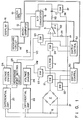
- Fig. 1 shows a circuit of a load cell type weight measuring device according to one embodiment of the present invention.
- This load cell type weight measuring device includes a load cell 2 which is constituted by connecting four strain gauge resistors in a bridge form; a driving power source E for supplying a driving voltage VE to the load cell 2; a low pass filter 4 for removing the AC component from an output signal of the load cell 2; and an amplifier circuit 6 for amplifying an output signal of the low pass filter 4.
- the amplifier circuit 6 includes an operation amplifier 6-1; and resistors Rl and R2 which are connected in series between an output terminal of the amplifier 6-1 and the ground, a junction between these resistors being coupled to an inverting input terminal of the amplifier 6-1.
- An output terminal of the amplifier 6 is coupled to an analog/digital converter 8 through a resistor R3 and a capacitor Cl.
- the A/D converter 8 is, for example, of the dual slope type and supplies to a microcomputer 12 a digital data NR corresponding to a difference between an input voltage VI and a reference voltage VR in response to an output pulse from a clock generator 10 for generating a clock pulse of a frequency f c .
- a keyboard circuit 14 which includes a sensitivity checking key and various function keys (not shown) and a display 16 are coupled to the microcomputer 12.
- Both ends of the driving power source E are coupled to respective input terminals of differential amplifier circuits 20 and 22.
- Output terminals of the differential amplifier circuits 20 and 22 are coupled to voltage dividers 24 and 26, respectively.
- the voltage divider 24 divides an output voltage of the differential amplifier circuit 20 and supplies the reference voltage VR to the A/D converter 8.
- a reference point setting circuit 28 divides the output voltage VR of the voltage divider 24 and generates an output voltage VO to set a reference operation point of the A/D converter 8.
- the voltage divider 26 divides an output voltage of the differential amplifier circuit 22 and supplies to the filter 4 a dummy rated voltage VM which is set equal to a rated output voltage generated from the load cell 2 when a rated weight is applied to the load cell 2.
- this load cell type weight measuring device includes switch control circuits 30 and 32; analog switches Sl to S3 which are controlled in response to control signals from the switch control circuit 30; and analog switches S4 to S6 which are controlled in response to control signals from the switch control circuit 32.
- the switch Sl is connected between the output terminal of the load cell 2 and the input terminal of the filter 4.
- the switch S2 is connected between the input terminal of the filter 4 and the ground.
- the switch S3 is connected between an output terminal of the voltage divider 26 and the input terminal of the filter 4.
- the switch S4 is connected between the output terminal of the filter 4 and a non-inverting input terminal of the operation amplifier 6-1.
- the switch S5 is connected between an output terminal of the reference point setting circuit 28 and the non-inverting input terminal of the operation amplifier 6-1.
- the switch S6 is connected between the input terminal of the A/D converter 8 and the ground.
- Fig. 2 shows a circuit of the differential amplifier circuits 20 and 22, the voltage dividers 24 and 26, and the reference point setting circuit 28.
- the differential amplifier circuit 20 includes buffer amplifiers 20-1 and 20-2 whose input terminals are respectively coupled to positive and negative terminals of the driving power source E; and a differential amplifier 20-3 whose inverting input terminal and non-inverting input terminal are respectively coupled to output terminals of the buffer amplifiers 20-1 and 20-2 through resistors R4 and R5. An output terminal of the differential amplifier 20-3 is connected through a resistor R6 to its inverting input terminal, while its non-inverting input terminal is grounded through a resistor R7.
- the differential amplifier circuit 22 includes buffer amplifiers 22-1 and 22-2, a differential amplifier 22-3, and resistors R8 to Rll which are connected in the same manner as the buffer amplifiers 20-1 and 20-2, differential amplifier 20-3 and resistors R4 to R7 of the differential amplifier circuit 20.
- the voltage divider 24 includes a resistor R12, a potentiometer RP1 and a resistor R13 which are connected in series between the output terminal of the differential amplifier 20-3 and the ground.
- a wiper terminal of the potentiometer RP1 is coupled to the A/D converter 8.
- the voltage divider 26 includes a resistor R14, a potentiometer RP2 and a resistor R15 which are connected in series between an output terminal of the differential amplifier 22-3 and the ground.
- a wiper terminal of the potentiometer RP2 is connected to the input terminal of the filter 4 through the switch S3.
- the reference point setting circuit 28 includes a buffer amplifier 28-1 whose input terminal is connected to the wiper terminal of the potentiometer RP1, and a resistor R16, a potentiometer RP3 and a resistor R17 which are connected in series between an output terminal of the buffer amplifier 28-1 and the ground.
- a wiper terminal of the potentiometer RP3 is connected to the non-inverting input terminal of the operation amplifier 6-1 through the switch S5.
- an output voltage V28 of the reference point setting circuit 28 is given by the following equation.
- the voltage dividing ratio k3 of the voltage divider 26 is determined so as to allow the output voltage V26 of the voltage divider 26 to be equal to the voltage V2 (N).
- a phase setting pulse signal as shown in Fig. 3A is generated in response to a clock pulse from, e.g., the clock generator 10.
- a control signal responsive to this phase setting pulse signal is supplied to the switch control circuit 32 and switch control signals shown in Figs. 3B and 3C are respectively supplied from this switch control 32 to the switch S4 and the switches S5 and S6.
- One cycle of this A/D converting operation is constituted by an offset correction phase Pl, an input signal integrating phase P2 and a reference signal integrating phase P3.
- the switch S4 is set into the OFF state and the switches S5 and S6 are set into the ON state, so that the output voltage V28 of the reference point setting circuit 28 is supplied to the operation amplifier 6-1.
- an output voltage V6 (Tl) of the amplifier circuit 6 will be given by the following equation.
- the digital output NR of the A/D converter 8 is given by the following equation.
- This equation (12) is implemented by reducing the input voltage V8 at a predetermined rate and counting the time until it reaches the reference level in the reference signal integrating phase P3.
- the interval of this reference signal integrating phase P3 is set into 2Tl.
- the microcomputer 12 gives a control signal to the switch control 30, thereby allowing this switch control 30 to supply switch control signals shown in Figs. 5A to 5C to the switches Sl to S3.
- intervals TF1 to TF13 in Figs. 5A to 5C are each equal to the interval of one operation cycle shown in Fig. 3A, and the offset correction phase Pl, input signal integrating phase P2 and reference signal integrating phase P3 are included in each interval.
- Figs. 5A to 5C when the weight measuring operation is executed for the intervals Tl and T2 and the sensitivity checking key is operated, the sensitivity checking examination is executed in the intervals TF3 to TF8. Namely, when the switch control signal shown in Fig. 5A is at a high level, the weight measuring mode is set and when the switch control signal of Fig. 5A is at a low level and when the switch Sl is closed, the sensitivity checking mode is set.
- a sensitivity data NRSP can be obtained from the difference between the digital output NR (S2) from the A/D converter 8 which is derived when the switch control signal of Fig. 5B is at a high level to keep the switch S2 ON and the digital output NR (S3) which is derived when the switch control signal of Fig. 5C is at a high level to keep the switch S3 ON.
- the switch S2 is closed in the interval TF3, so that the input voltage of 0V is supplied through the filter 4 and switch S4 to the amplifier circuit 6 in the input signal integrating phase P2 and reference signal integrating phase P3.
- This digital output NR (S2) is stored in a memory (not shown) in the microcomputer 12.
- the similar operation is executed, for example, even in the subsequent intervals T4 and T5 and the digital data derived in the respective intervals T3 to T5 are checked to see if they are stable or not.
- the output voltage of the voltage divider 26 is supplied to the amplifier circuit 6 through the filter 4 and switch S4.
- the digital output data NR (S3) from the A/D converter 8 will be given by the following equation.
- This digital output data NR (S3) is also stored in the memory in the microcomputer 12.
- the digital data derived in the intervals TF6, TF7 and TF8 in this way are checked to see if they are stable or not. After they were confirmed to be stable, the sensitivity calculation is immediately executed.
- the microcomputer 12 calculates the difference between the digital output data NR (S2) and NR (S3) stored in the memory to obtain the sensitivity data NRSP represented by the following equation.
- This sensitivity data NRSP is compared with a sensitivity reference value NRRF which has been preset by the microcomputer 12.
- a sensitivity reference value NRRF which has been preset by the microcomputer 12.
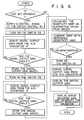
- Fig. 6 shows the flowchart to explain the operation of the load cell type weight measuring device shown in Figs. 1 and 2.
- the microcomputer 12 When it is detected that the sensitivity checking key was operated, the microcomputer 12 first turns on the switch S2 to execute the sensitivity checking examination and turns off the switches Sl and S3. In this state, the digital output data NR (S2) is generated from the A/D converter 8 as indicated in equation (16). In this embodiment, the digital output data are respectively derived in three operation cycles (e.g., intervals TF3, TF4 and TF5). In the case where the maximum error among these three digital output data is less than a predetermined value, one of the three digital output data is stored in the memory as the effective data NR (S2). Then, the switches Sl and S2 are turned off and the switch S3 is turned on.
- the switch Sl and S2 are turned off and the switch S3 is turned on.
- the digital output data NR (S3) is generated from the A/D converter 8 as indicated by equation (17). Also, in this case, the digital output data are respectively derived in three operation cycles (e.g., intervals TF6 to TF8). In the case where the maximum error among these three digital output data is less than a predetermined value, one of the three digital output data is stored in the memory as the effective data NR (S3). Subsequently, the sensitivity NRSP is calculated by subtracting the digital output data NR (S2) from the digital output data NR (S3). The difference between this sensitivity NRSP and the reference sensitivity NRRF is obtained and this difference is checked to see if it is within the permissible range ⁇ or not.
- the switches S2 and S3 are turned off and the switch Sl is turned on, thereby executing the weight measuring operation.
- the weight measurement data obtained from the A/D converter 8 in this way is displayed on the display 16.
- the microcomputer 12 executes the error indication and at the same time it interrupts the weight measuring operation.
- the present invention has been described in the above with respect to one embodiment, the invention is not limited to only this embodiment.
- the A/D converter 8 of the dual slope type has been used, any other type of A/D converter which is ordinarily well known may be also used.
- the sensitivity checking key has been used in the foregoing embodiment, it is possible to omit this sensitivity checking key and to automatically set the sensitivity checking mode and weight measuring mode alternately.
Abstract
Description
- The present invention relates to a load cell type weight measuring device and a sensitivity checking method thereof.
- Generally, a high degree of accuracy is required for load cell type weight measuring devices and, in particular, the authorized examination regarding the measurement precision is severe in West Germany and Switzerland. In this point, since the type of load cell itself has been authorized, no problem will be caused in particular. However, even when the load cell whose type has been authorized in this way is used, if the operation of the circuit section is not normal, the weight measurement cannot be performed accurately. Particularly, in the load cell type weight measuring device, to keep the relation between the weight and the measurement signal to be linear at least within a measurement range, it is necessary to always maintain the sensitivity of the load cell type weight measuring device to be a predetermined value. For this purpose, although the sensitivity checking examination is needed to be performed for the load cell type weight measuring device, the conventional load cell type weight measuring device did not have an appropriate sensitivity checking examination function.
- It is an object of the present invention to provide a load cell type weight measuring device having a sensitivity checking function.
- Another object of the invention is to provide a sensitivity checking method in the load cell type weight measuring device.
- These objects are accomplished by a load cell type weight measuring device comprising a load cell producing an output voltage corresponding to the weight applied thereto; a rated voltage generating circuit for generating an output voltage equal to the output voltage generated by this load cell which is applied with a rated weight; an amplifier circuit; a switching circuit for selectively coupling one of the load cell, rated voltage generating circuit and reference potential terminal with the amplifier circuit; an analog/digital converter for converting an output voltage of the amplifier circuit to digital data; and a data processing unit which gives control signals to the switching circuit and inhibits the output data of the analog/digital converter from being supplied as effective weight measurement data when the data processing unit detects that the difference between two items of output digital data of the analog/digital converter which are respectively obtained when the rated voltage generating circuit and reference potential terminal are coupled with the amplifier circuit, exceeds a predetermined range.
- In this invention, the rated voltage generating circuit and reference potential terminal are coupled with the amplifier circuit at different timings by the switching circuit, and the sensitivity of this load cell type weight measuring device can be easily checked on the basis of the digital data derived at this time from the analog/digital converter.
- This invention can be more fully understood from the following detailed description when taken in conjunction with the accompanying drawings, in which:
- Fig. 1 is a circuit diagram of a load cell type weight measuring device according to one embodiment of the present invention;
- Fig. 2 is a circuit diagram of differential amplifiers, voltage dividers and reference point setting circuit shown in Fig. 1;
- Figs. 3A to 3C are signal waveform diagrams to describe the operation of an A/D converter shown in Fig. 1;
- Fig. 4 shows the relation between the weight which is applied to a load cell shown in Fig. 1 and digital output data from the A/D converter;
- Figs. 5A to 5C are signal waveform diagrams to explain the sensitivity checking operation of the load cell type weight measuring device shown in Fig. 1; and
- Fig. 6 is a flowchart to explain the operation of the load cell type weight measuring device shown in Fig. 1.
- Fig. 1 shows a circuit of a load cell type weight measuring device according to one embodiment of the present invention. This load cell type weight measuring device includes a load cell 2 which is constituted by connecting four strain gauge resistors in a bridge form; a driving power source E for supplying a driving voltage VE to the load cell 2; a
low pass filter 4 for removing the AC component from an output signal of the load cell 2; and anamplifier circuit 6 for amplifying an output signal of thelow pass filter 4. Theamplifier circuit 6 includes an operation amplifier 6-1; and resistors Rl and R2 which are connected in series between an output terminal of the amplifier 6-1 and the ground, a junction between these resistors being coupled to an inverting input terminal of the amplifier 6-1. An output terminal of theamplifier 6 is coupled to an analog/digital converter 8 through a resistor R3 and a capacitor Cl. The A/D converter 8 is, for example, of the dual slope type and supplies to a microcomputer 12 a digital data NR corresponding to a difference between an input voltage VI and a reference voltage VR in response to an output pulse from aclock generator 10 for generating a clock pulse of a frequency fc. Akeyboard circuit 14 which includes a sensitivity checking key and various function keys (not shown) and adisplay 16 are coupled to themicrocomputer 12. - Both ends of the driving power source E are coupled to respective input terminals of
differential amplifier circuits differential amplifier circuits voltage dividers voltage divider 24 divides an output voltage of thedifferential amplifier circuit 20 and supplies the reference voltage VR to the A/D converter 8. A referencepoint setting circuit 28 divides the output voltage VR of thevoltage divider 24 and generates an output voltage VO to set a reference operation point of the A/D converter 8. In addition, thevoltage divider 26 divides an output voltage of thedifferential amplifier circuit 22 and supplies to the filter 4 a dummy rated voltage VM which is set equal to a rated output voltage generated from the load cell 2 when a rated weight is applied to the load cell 2. - Furthermore, this load cell type weight measuring device includes
switch control circuits switch control circuit 30; and analog switches S4 to S6 which are controlled in response to control signals from theswitch control circuit 32. The switch Sl is connected between the output terminal of the load cell 2 and the input terminal of thefilter 4. The switch S2 is connected between the input terminal of thefilter 4 and the ground. The switch S3 is connected between an output terminal of thevoltage divider 26 and the input terminal of thefilter 4. The switch S4 is connected between the output terminal of thefilter 4 and a non-inverting input terminal of the operation amplifier 6-1. The switch S5 is connected between an output terminal of the referencepoint setting circuit 28 and the non-inverting input terminal of the operation amplifier 6-1. The switch S6 is connected between the input terminal of the A/D converter 8 and the ground. - Fig. 2 shows a circuit of the
differential amplifier circuits voltage dividers point setting circuit 28. - The
differential amplifier circuit 20 includes buffer amplifiers 20-1 and 20-2 whose input terminals are respectively coupled to positive and negative terminals of the driving power source E; and a differential amplifier 20-3 whose inverting input terminal and non-inverting input terminal are respectively coupled to output terminals of the buffer amplifiers 20-1 and 20-2 through resistors R4 and R5. An output terminal of the differential amplifier 20-3 is connected through a resistor R6 to its inverting input terminal, while its non-inverting input terminal is grounded through a resistor R7. Thedifferential amplifier circuit 22 includes buffer amplifiers 22-1 and 22-2, a differential amplifier 22-3, and resistors R8 to Rll which are connected in the same manner as the buffer amplifiers 20-1 and 20-2, differential amplifier 20-3 and resistors R4 to R7 of thedifferential amplifier circuit 20. - The
voltage divider 24 includes a resistor R12, a potentiometer RP1 and a resistor R13 which are connected in series between the output terminal of the differential amplifier 20-3 and the ground. A wiper terminal of the potentiometer RP1 is coupled to the A/D converter 8. On the other hand, thevoltage divider 26 includes a resistor R14, a potentiometer RP2 and a resistor R15 which are connected in series between an output terminal of the differential amplifier 22-3 and the ground. A wiper terminal of the potentiometer RP2 is connected to the input terminal of thefilter 4 through the switch S3. - The reference
point setting circuit 28 includes a buffer amplifier 28-1 whose input terminal is connected to the wiper terminal of the potentiometer RP1, and a resistor R16, a potentiometer RP3 and a resistor R17 which are connected in series between an output terminal of the buffer amplifier 28-1 and the ground. A wiper terminal of the potentiometer RP3 is connected to the non-inverting input terminal of the operation amplifier 6-1 through the switch S5. - Assuming that R4 = R5 and R6 = R7 in the
differential amplifier circuit 20 shown in Fig. 2, an output voltage V20 represented by the following equation will be supplied from thedifferential amplifier circuit 20.
- Now, assuming that a voltage dividing ratio of the
voltage divider 24 is kl, an output voltage V24 or VR of thevoltage divider 24 is given by the following equation.
- Assuming that an amplification factor of the buffer amplifier 28-1 is 1 and a voltage dividing ratio of the voltage divider which is constituted by the resistor R16, potentiometer RP3 and resistor R17 is k2, an output voltage V28 of the reference
point setting circuit 28 is given by the following equation.
- In addition, assuming that R8 = R9 and R10 = Rll in the
differential amplifier circuit 22, an output voltage V22 of thedifferential amplifier circuit 22 is given by the following equation.
- Assuming that a voltage dividing ratio of the
voltage divider 26 is k3, an output voltage V26 of thisvoltage divider 26 is given by the following equation.
- Although an output voltage V2 in proportion to a weight FX (kg) is generated from the load cell 2, this output voltage V2 is given by the following equation when it is assumed that a rated weight of the load cell 2 is FN (kg) and a sensitivity is k (v/v) and a zero-balance is VB (V).

- In the case where FX = 0, an output voltage V2 (0) which is equal to the zero-balance voltage VB is generated from the load cell 2.
- Also, in the case where FX = FN, the output voltage V2 (N) which is equal to (k·VE + VB) is generated from the load cell 2. Therefore, a voltage span VSP of the load cell 2 is given by the following equation.

- In this embodiment, since two dummy load cell output voltages having the voltage span VSP are applied to the
filter 4 in the sensitivity checking mode, the voltage dividing ratio k3 of thevoltage divider 26 is determined so as to allow the output voltage V26 of thevoltage divider 26 to be equal to the voltage V2 (N). - The A/D converting operation of the load cell type weight measuring device shown in Figs. 1 and 2 will then be described with reference to Figs. 3A to 3C.
- In the A/
D converter 8, a phase setting pulse signal as shown in Fig. 3A is generated in response to a clock pulse from, e.g., theclock generator 10. A control signal responsive to this phase setting pulse signal is supplied to theswitch control circuit 32 and switch control signals shown in Figs. 3B and 3C are respectively supplied from thisswitch control 32 to the switch S4 and the switches S5 and S6. One cycle of this A/D converting operation is constituted by an offset correction phase Pl, an input signal integrating phase P2 and a reference signal integrating phase P3. - In the offset correction phase Pl, the switch S4 is set into the OFF state and the switches S5 and S6 are set into the ON state, so that the output voltage V28 of the reference
point setting circuit 28 is supplied to the operation amplifier 6-1. In this case, assuming that an offset voltage of the operation amplifier 6-1 is VOF, an output voltage V6 (Tl) of theamplifier circuit 6 will be given by the following equation.
- Also, in this case, since the switch S6 is in the ON state, in the case where it is possible to regard an input impedance of the A/
D converter 8 as infinity, the capacitor Cl is charged toward the voltage V6 (Tl). A charging voltage VC of the capacitor Cl while it is charging is given by the following equation.
- In the input signal integrating phase P2, since the switch S4 is set into the ON state and the switches S5 and S6 are set into the OFF state, the output voltage V4 of the
filter 4 is supplied to theamplifier circuit 6. At this time, the output voltage V6 (T2) of theamplifier circuit 6 will be given by the following equation.
- Due to this, an input voltage V8 represented by the following equation is supplied to the A/
D converter 8.
- Assuming that the digital data corresponding to an interval T2 of the input signal integrating phase P2 is NS (= fc x T2), the digital output NR of the A/
D converter 8 is given by the following equation.
- This equation (12) is implemented by reducing the input voltage V8 at a predetermined rate and counting the time until it reaches the reference level in the reference signal integrating phase P3. The interval of this reference signal integrating phase P3 is set into 2Tl.
- By substituting equation (2), (3) and (11) for this equation (12), the following equation is derived.

- Assuming now that the switch Sl is set into the ON state and the switches S2 and S3 are set into the OFF state. In this case, the output voltage V2 of the load cell 2 is supplied to the
amplifier circuit 6 through thefilter 4. When V2 = V4, by substituting equation (6) for equation (13), the following equation is derived.
- Since VB varies in proportional to VE, NR will not be subjected to the fluctuation of VE.
- Now, assuming that the digital output when FX = 0 is NR (0) and the digital output when FX = FN is NR (N), the span NSP of the digital output is given by the following equation.

- In this case, if (


D converter 8 can be doubled. Namely, as shown in Fig. 4, by setting the digital output of the A/D converter 8 into 0 when FX = FN/2 and by setting the input/output characteristics of the A/D converter 8 so that NR (N) = - NR (0), the resolution power of the A/D converter 8 can be doubled. - Next, the sensitivity checking examination of the load cell type weight measuring device shown in Figs. 1 and 2 will be described.
- The
microcomputer 12 gives a control signal to theswitch control 30, thereby allowing thisswitch control 30 to supply switch control signals shown in Figs. 5A to 5C to the switches Sl to S3. In addition, intervals TF1 to TF13 in Figs. 5A to 5C are each equal to the interval of one operation cycle shown in Fig. 3A, and the offset correction phase Pl, input signal integrating phase P2 and reference signal integrating phase P3 are included in each interval. - In Figs. 5A to 5C, when the weight measuring operation is executed for the intervals Tl and T2 and the sensitivity checking key is operated, the sensitivity checking examination is executed in the intervals TF3 to TF8. Namely, when the switch control signal shown in Fig. 5A is at a high level, the weight measuring mode is set and when the switch control signal of Fig. 5A is at a low level and when the switch Sl is closed, the sensitivity checking mode is set. A sensitivity data NRSP can be obtained from the difference between the digital output NR (S2) from the A/
D converter 8 which is derived when the switch control signal of Fig. 5B is at a high level to keep the switch S2 ON and the digital output NR (S3) which is derived when the switch control signal of Fig. 5C is at a high level to keep the switch S3 ON. - For instance, when the sensitivity checking key is operated in the interval TF2, the switch S2 is closed in the interval TF3, so that the input voltage of 0V is supplied through the
filter 4 and switch S4 to theamplifier circuit 6 in the input signal integrating phase P2 and reference signal integrating phase P3. In this case, the digital output NR (S2) of the A/D converter 8 will be given by the following equation if V4 = 0 in equation (13).
- This digital output NR (S2) is stored in a memory (not shown) in the
microcomputer 12. The similar operation is executed, for example, even in the subsequent intervals T4 and T5 and the digital data derived in the respective intervals T3 to T5 are checked to see if they are stable or not. In the interval T6 immediately after the digital data were confirmed to be stable, when the switch S2 is opened and the switch S3 is closed, the output voltage of thevoltage divider 26 is supplied to theamplifier circuit 6 through thefilter 4 and switch S4. In this case, since the output voltage V26 shown in equation (5) is generated from thevoltage divider 26, the digital output data NR (S3) from the A/D converter 8 will be given by the following equation.
- This digital output data NR (S3) is also stored in the memory in the
microcomputer 12. The digital data derived in the intervals TF6, TF7 and TF8 in this way are checked to see if they are stable or not. After they were confirmed to be stable, the sensitivity calculation is immediately executed. - As is obvious from equations (16) and (17), since both digital outputs NR (S2) and NR (S3) are independent from the voltage VE, the digital output data NR (S2) and NR (S3) do not vary in dependence upon the variation in this power source voltage VE.
- The
microcomputer 12 calculates the difference between the digital output data NR (S2) and NR (S3) stored in the memory to obtain the sensitivity data NRSP represented by the following equation. -

- This sensitivity data NRSP is compared with a sensitivity reference value NRRF which has been preset by the
microcomputer 12. When the difference between them is within a permissible range of ±a the digital output to be obtained in the weight measuring mode after, e.g., interval TF9 is displayed as the effective weight data on thedisplay 16. On the other hand, when the difference between them exceeds the permissible range of ±a, the digital output data derived during the measurement interval is made invalid and the invalid data is displayed on thedisplay 16. - Fig. 6 shows the flowchart to explain the operation of the load cell type weight measuring device shown in Figs. 1 and 2.
- When it is detected that the sensitivity checking key was operated, the
microcomputer 12 first turns on the switch S2 to execute the sensitivity checking examination and turns off the switches Sl and S3. In this state, the digital output data NR (S2) is generated from the A/D converter 8 as indicated in equation (16). In this embodiment, the digital output data are respectively derived in three operation cycles (e.g., intervals TF3, TF4 and TF5). In the case where the maximum error among these three digital output data is less than a predetermined value, one of the three digital output data is stored in the memory as the effective data NR (S2). Then, the switches Sl and S2 are turned off and the switch S3 is turned on. In this state, the digital output data NR (S3) is generated from the A/D converter 8 as indicated by equation (17). Also, in this case, the digital output data are respectively derived in three operation cycles (e.g., intervals TF6 to TF8). In the case where the maximum error among these three digital output data is less than a predetermined value, one of the three digital output data is stored in the memory as the effective data NR (S3). Subsequently, the sensitivity NRSP is calculated by subtracting the digital output data NR (S2) from the digital output data NR (S3). The difference between this sensitivity NRSP and the reference sensitivity NRRF is obtained and this difference is checked to see if it is within the permissible range ±α or not. If it is detected that the difference is within the permissible range, the switches S2 and S3 are turned off and the switch Sl is turned on, thereby executing the weight measuring operation. The weight measurement data obtained from the A/D converter 8 in this way is displayed on thedisplay 16. In contrast, in the case where it is detected that the difference between the NRSP and the NRRF is out of the permissible range of ±a, themicrocomputer 12 executes the error indication and at the same time it interrupts the weight measuring operation. - Although the present invention has been described in the above with respect to one embodiment, the invention is not limited to only this embodiment. For instance, although the A/
D converter 8 of the dual slope type has been used, any other type of A/D converter which is ordinarily well known may be also used. In addition, although the sensitivity checking key has been used in the foregoing embodiment, it is possible to omit this sensitivity checking key and to automatically set the sensitivity checking mode and weight measuring mode alternately. In such a case, for example, under the control of themicrocomputer 12, it is possible to close the switch Sl for six operation cycles and set the weight measuring mode, then to sequentially close the switches S2 and S3 in this sequence for three operation cycles, respectively, and set the sensitivity checking mode, thereby alternately setting the weight measuring mode and sensitivity checking mode.
Claims (8)
characterized by further comprising: rated voltage generating means (22, 26) for generating an output voltage equal to the output voltage generated from said load cell which is applied with a rated weight; switching means (Sl to S3, 30) for selectively connecting one of said load cell (2), said rated voltage generating means (22, 26) and said reference potential terminal to said amplifier means (6); and data processing means (12) for controlling said switching means (Sl to S3, 30), and inhibiting the output data of said analog/digital converting means (8) from being supplied as effective weight measurement data when it is detected that the difference between two items of digital data generated from said analog/digital converting means (8), one obtained when said rated voltage generating means (22, 26) is connected to said amplifier means (6) and the other obtained when said reference potential terminal is coupled to said amplifier means (6), exceeds a predetermined range.
Applications Claiming Priority (4)
| Application Number | Priority Date | Filing Date | Title |
|---|---|---|---|
| JP10348083A JPS59228120A (en) | 1983-06-09 | 1983-06-09 | Load cell scale |
| JP103480/83 | 1983-06-09 | ||
| JP10348183A JPS59228122A (en) | 1983-06-09 | 1983-06-09 | Sensitivity testing method for load cell scale |
| JP103481/83 | 1983-06-09 |
Publications (3)
| Publication Number | Publication Date |
|---|---|
| EP0128559A2 true EP0128559A2 (en) | 1984-12-19 |
| EP0128559A3 EP0128559A3 (en) | 1986-02-05 |
| EP0128559B1 EP0128559B1 (en) | 1988-09-21 |
Family
ID=26444117
Family Applications (1)
| Application Number | Title | Priority Date | Filing Date |
|---|---|---|---|
| EP84106584A Expired EP0128559B1 (en) | 1983-06-09 | 1984-06-08 | A load cell type weight measuring device and a sensitivity checking method thereof |
Country Status (3)
| Country | Link |
|---|---|
| US (1) | US4580644A (en) |
| EP (1) | EP0128559B1 (en) |
| DE (1) | DE3474210D1 (en) |
Cited By (2)
| Publication number | Priority date | Publication date | Assignee | Title |
|---|---|---|---|---|
| EP0145433A2 (en) * | 1983-12-03 | 1985-06-19 | Kabushiki Kaisha Ishida Koki Seisakusho | Electronic weigher |
| GB2238416A (en) * | 1989-11-23 | 1991-05-29 | Bosch Gmbh Robert | Circuit arrangement for detecting signal faults |
Families Citing this family (5)
| Publication number | Priority date | Publication date | Assignee | Title |
|---|---|---|---|---|
| US4705126A (en) * | 1985-09-24 | 1987-11-10 | Ishida Scales Manufacturing Company, Ltd. | Signal processing circuit and weighing apparatus incorporating same |
| JPH076823B2 (en) * | 1986-03-25 | 1995-01-30 | 東京電気株式会社 | Load cell balance resistance adjustment method |
| GB2340951B (en) * | 1998-08-20 | 2000-07-12 | Gec Avery Ltd | Weight simulation calibration rig and method |
| US6079122A (en) * | 1998-08-28 | 2000-06-27 | Rajkovich; Thomas Russell | Weighing dryer |
| US6460008B1 (en) * | 2000-07-19 | 2002-10-01 | Ivan E. Hardt | Yield monitoring system for grain harvesting combine |
Citations (5)
| Publication number | Priority date | Publication date | Assignee | Title |
|---|---|---|---|---|
| US4158396A (en) * | 1977-04-22 | 1979-06-19 | Tokyo Electric Co., Ltd. | Electronic weight measuring device |
| EP0007288A1 (en) * | 1978-07-14 | 1980-01-23 | Terraillon | Arrangement for measuring the intensity of a force which is transversally exerted on the free end of a flexion beam |
| GB2050622A (en) * | 1979-05-15 | 1981-01-07 | Tokyo Electric Co Ltd | Electronic weight measuring device |
| GB2080540A (en) * | 1980-06-21 | 1982-02-03 | Salter & Co Ltd G | Electrical apparatus for weighing animals |
| US4364027A (en) * | 1980-09-16 | 1982-12-14 | Sony/Tektronix | Calibration apparatus for analog-to-digital converter |
Family Cites Families (3)
| Publication number | Priority date | Publication date | Assignee | Title |
|---|---|---|---|---|
| US3728626A (en) * | 1971-03-25 | 1973-04-17 | Colt Ind Operating Corp | Electronic measuring system |
| EP0044707B1 (en) * | 1980-07-17 | 1987-10-14 | Kabushiki Kaisha Shimadzu Seisakusho | An electronic balance |
| US4535854A (en) * | 1982-11-16 | 1985-08-20 | Pennsylvania Scale Company | Calibration method and apparatus for an electronic weight indicator |
-
1984
- 1984-06-01 US US06/616,557 patent/US4580644A/en not_active Expired - Lifetime
- 1984-06-08 EP EP84106584A patent/EP0128559B1/en not_active Expired
- 1984-06-08 DE DE8484106584T patent/DE3474210D1/en not_active Expired
Patent Citations (5)
| Publication number | Priority date | Publication date | Assignee | Title |
|---|---|---|---|---|
| US4158396A (en) * | 1977-04-22 | 1979-06-19 | Tokyo Electric Co., Ltd. | Electronic weight measuring device |
| EP0007288A1 (en) * | 1978-07-14 | 1980-01-23 | Terraillon | Arrangement for measuring the intensity of a force which is transversally exerted on the free end of a flexion beam |
| GB2050622A (en) * | 1979-05-15 | 1981-01-07 | Tokyo Electric Co Ltd | Electronic weight measuring device |
| GB2080540A (en) * | 1980-06-21 | 1982-02-03 | Salter & Co Ltd G | Electrical apparatus for weighing animals |
| US4364027A (en) * | 1980-09-16 | 1982-12-14 | Sony/Tektronix | Calibration apparatus for analog-to-digital converter |
Cited By (3)
| Publication number | Priority date | Publication date | Assignee | Title |
|---|---|---|---|---|
| EP0145433A2 (en) * | 1983-12-03 | 1985-06-19 | Kabushiki Kaisha Ishida Koki Seisakusho | Electronic weigher |
| EP0145433A3 (en) * | 1983-12-03 | 1986-04-16 | Kabushiki Kaisha Ishida Koki Seisakusho | Electronic weigher |
| GB2238416A (en) * | 1989-11-23 | 1991-05-29 | Bosch Gmbh Robert | Circuit arrangement for detecting signal faults |
Also Published As
| Publication number | Publication date |
|---|---|
| DE3474210D1 (en) | 1988-10-27 |
| US4580644A (en) | 1986-04-08 |
| EP0128559B1 (en) | 1988-09-21 |
| EP0128559A3 (en) | 1986-02-05 |
Similar Documents
| Publication | Publication Date | Title |
|---|---|---|
| EP0144834B1 (en) | Load cell type weight-measuring device | |
| US4816745A (en) | Method and arrangement for measuring the resistance ratio in a resistance half-bridge | |
| EP0128559B1 (en) | A load cell type weight measuring device and a sensitivity checking method thereof | |
| US4294322A (en) | Electronic weight measuring device | |
| US4417631A (en) | Zero tracking circuit for electronic weighing scale | |
| US4149605A (en) | Scale with digital display | |
| EP0100103B1 (en) | A pulse width modulation circuit and an analog product forming integration circuit using such modulation circuit | |
| US4549623A (en) | Apparatus for automatically monitoring a constant current source in a measuring instrument | |
| US5014058A (en) | Method and arrangement for evaluating a measurable analog electrical quantity | |
| US4445111A (en) | Bi-polar electronic signal converters with single polarity accurate reference source | |
| EP0058050A1 (en) | Measuring method | |
| US4248316A (en) | Error detecting apparatus for a scale having a digital display | |
| JPH0365513B2 (en) | ||
| SU690504A1 (en) | Integrator | |
| SU1686314A1 (en) | Digital strain-measuring device | |
| RU2003995C1 (en) | Device for measuring and checking parameters of voltage stabilizers | |
| SU1092435A1 (en) | Method and device for locating power line damage | |
| SU1182418A2 (en) | Voltage converter | |
| SU1118939A1 (en) | Device for measuring direct current mains insulation resistance | |
| SU1231489A1 (en) | Device for determining parameters of second-order dynamic element | |
| SU994928A1 (en) | Digital measuring device for strain-gauge balance | |
| SU1167625A1 (en) | Logarithmic function generator | |
| JPS59228120A (en) | Load cell scale | |
| SU1164558A1 (en) | Digital meter for strain-measuring balance | |
| SU1476319A1 (en) | Electronic clock |
Legal Events
| Date | Code | Title | Description |
|---|---|---|---|
| PUAI | Public reference made under article 153(3) epc to a published international application that has entered the european phase |
Free format text: ORIGINAL CODE: 0009012 |
|
| AK | Designated contracting states |
Designated state(s): DE GB |
|
| PUAL | Search report despatched |
Free format text: ORIGINAL CODE: 0009013 |
|
| AK | Designated contracting states |
Designated state(s): DE GB |
|
| 17P | Request for examination filed |
Effective date: 19860724 |
|
| 17Q | First examination report despatched |
Effective date: 19870930 |
|
| GRAA | (expected) grant |
Free format text: ORIGINAL CODE: 0009210 |
|
| AK | Designated contracting states |
Kind code of ref document: B1 Designated state(s): DE GB |
|
| REF | Corresponds to: |
Ref document number: 3474210 Country of ref document: DE Date of ref document: 19881027 |
|
| PLBE | No opposition filed within time limit |
Free format text: ORIGINAL CODE: 0009261 |
|
| STAA | Information on the status of an ep patent application or granted ep patent |
Free format text: STATUS: NO OPPOSITION FILED WITHIN TIME LIMIT |
|
| 26N | No opposition filed | ||
| PGFP | Annual fee paid to national office [announced via postgrant information from national office to epo] |
Ref country code: DE Payment date: 20010605 Year of fee payment: 18 |
|
| PGFP | Annual fee paid to national office [announced via postgrant information from national office to epo] |
Ref country code: GB Payment date: 20010606 Year of fee payment: 18 |
|
| REG | Reference to a national code |
Ref country code: GB Ref legal event code: IF02 |
|
| PG25 | Lapsed in a contracting state [announced via postgrant information from national office to epo] |
Ref country code: GB Free format text: LAPSE BECAUSE OF NON-PAYMENT OF DUE FEES Effective date: 20020608 |
|
| PG25 | Lapsed in a contracting state [announced via postgrant information from national office to epo] |
Ref country code: DE Free format text: LAPSE BECAUSE OF NON-PAYMENT OF DUE FEES Effective date: 20030101 |
|
| GBPC | Gb: european patent ceased through non-payment of renewal fee |
Effective date: 20020608 |