EP0130614A2 - Semiconductor memory using multiple level storage structure - Google Patents
Semiconductor memory using multiple level storage structure Download PDFInfo
- Publication number
- EP0130614A2 EP0130614A2 EP84107724A EP84107724A EP0130614A2 EP 0130614 A2 EP0130614 A2 EP 0130614A2 EP 84107724 A EP84107724 A EP 84107724A EP 84107724 A EP84107724 A EP 84107724A EP 0130614 A2 EP0130614 A2 EP 0130614A2
- Authority
- EP
- European Patent Office
- Prior art keywords
- charge
- charge storage
- level
- row address
- voltage
- Prior art date
- Legal status (The legal status is an assumption and is not a legal conclusion. Google has not performed a legal analysis and makes no representation as to the accuracy of the status listed.)
- Granted
Links
Images


Classifications
-
- G—PHYSICS
- G11—INFORMATION STORAGE
- G11C—STATIC STORES
- G11C11/00—Digital stores characterised by the use of particular electric or magnetic storage elements; Storage elements therefor
- G11C11/21—Digital stores characterised by the use of particular electric or magnetic storage elements; Storage elements therefor using electric elements
- G11C11/34—Digital stores characterised by the use of particular electric or magnetic storage elements; Storage elements therefor using electric elements using semiconductor devices
- G11C11/40—Digital stores characterised by the use of particular electric or magnetic storage elements; Storage elements therefor using electric elements using semiconductor devices using transistors
- G11C11/401—Digital stores characterised by the use of particular electric or magnetic storage elements; Storage elements therefor using electric elements using semiconductor devices using transistors forming cells needing refreshing or charge regeneration, i.e. dynamic cells
-
- G—PHYSICS
- G11—INFORMATION STORAGE
- G11C—STATIC STORES
- G11C19/00—Digital stores in which the information is moved stepwise, e.g. shift registers
-
- G—PHYSICS
- G11—INFORMATION STORAGE
- G11C—STATIC STORES
- G11C11/00—Digital stores characterised by the use of particular electric or magnetic storage elements; Storage elements therefor
- G11C11/56—Digital stores characterised by the use of particular electric or magnetic storage elements; Storage elements therefor using storage elements with more than two stable states represented by steps, e.g. of voltage, current, phase, frequency
- G11C11/565—Digital stores characterised by the use of particular electric or magnetic storage elements; Storage elements therefor using storage elements with more than two stable states represented by steps, e.g. of voltage, current, phase, frequency using capacitive charge storage elements
-
- G—PHYSICS
- G11—INFORMATION STORAGE
- G11C—STATIC STORES
- G11C8/00—Arrangements for selecting an address in a digital store
- G11C8/04—Arrangements for selecting an address in a digital store using a sequential addressing device, e.g. shift register, counter
Definitions
- This invention relates to a semiconductor memory, and more particularly to a semiconductor integrated .circuit memory.
- a semiconductor memory having a high integration density stores data by making the existence and absence of charge inside a potential well on a semiconductor surface correspond to digital signals "1" and "0".
- this storing method involves the problem that in the case of DRAM, for example, only binary 1- digit (1-bit) data can be handled for each unit memory cell, and hence the amount of total bits per chip is limited.
- the CCD memory has a structure in which the stored charge is cycled using a transfer electrode.
- the stored charge is transferred along a CCD transfer electrode loop arranged cyclicly, and the charge must be read and written at an input-output portion disposed at a predetermined position inside the CCD loop on a certain cycle-of time.
- a great deal of power is necessary to charge and discharge the transfer electrodes for transferring the charge in order to refresh all data, and it has therefore been difficult in the past to provide a memory having low power consumption.
- DRAM semiconductor dynamic random access memory
- memory cells unit memory cells
- semiconductor memories using multiple level storage structure are believed to be effective means that can realize very high integration density semiconductor memories and are available in accordance with the existing process technique.
- the memory improves substantially the integration density by storing data of at least more than two levels per memory cell.
- CCD charge coupled device
- the multi-level storage memory using the charge coupled devices has not much been put into practical application for the following reasons.
- the present invention is therefore directed to provide a multi-level storage semiconductor memory (MLS memory) which eliminates the problems described above and can simultaneously accomplish low power consumption and large memory capacity.
- MLS memory multi-level storage semiconductor memory
- the present invention realizes a very high integration density MLS memory by introducing a novel concept that has not been known in the past.
- the present invention can provide a large capacity memory which has low power consumption but can select at random memory cells.
- the present invention introduces an entirely novel concept that a multi-level step voltage is applied to a word line or a plate so as to read the data at the timing at which stored charge flows out, and writes the data to the memory cell at the timing which corresponds to an input signal.
- the present invention can realize efficiently a very high density semiconductor memory on the basis of this novel concept.
- Figure 1 illustrates the sectional structure of a memory cell in accordance with the first principle of the invention and the kind of applied voltages.
- the memory based on the later- appearing principle will be hereinafter called a "word gate driving MLS memory".
- word gate driving MLS memory the memory based on the later- appearing principle.
- the electron is dealt with as the stored charge, the principle can be applied exactly in the same way to the positive hole by converting the conductivity type of a semiconductor and inverting the voltage for operating the memory.
- reference numeral 10 represents a p-type semiconductor layer (a substrate of a semiconductor layer disposed on the substrate), reference numeral 11 is a gate insulating film (oxidized film or the like), and reference numerals 12 and 13 are electrodes formed on the gate insulating film.
- Reference numerals 14 and 15 represents highly doped n-type semiconductor layers formed in self-alignment with the electrodes by ion implantation, or the like, respectively.
- the electrode 13 corresponds to the gate of an insulated gate field effect transistor (MOS-FET), and the n-type semiconductor layers 14 and 15 correspond to the drain or source of the transistor.
- MOS-FET insulated gate field effect transistor
- the gate 13 of MOS-FET is connected to an address decoded row line (word line) 2, and the drain 14, to an address decoded column line (bit line) 3 to form a memory matrix.
- the electrode 12 is connected in common to all the memory cells, and a positive D.C. voltage is applied to it.
- Figures 2A, 2B and 2C illustrate the surface potential to the electrons along the surface of the semiconductor layer of the memory cell shown in Figure 1.
- Figure 2A illustrates the charge storage mode.
- the stored charge 20 in the potential well 21 below the plate is isolated from the bit line 23 by a potential barrier 22 below the gate of MOS-FET, and from the other regions by the potential barrier of an isolation region disposed around the memory cell.
- multi-level step voltages ⁇ w (30, 31, 32) that shifts from a low voltage to a high voltage are applied to the word line.2 as shown in Fig. 3.
- reference numeral 30 corresponds to Figure 2A, 31 to Figure 2B, and 32 to Figure 2C.
- FIG. 2A, 2B and 2C illustrates the mode of drop of the bit line voltage VD (33, 34) caused by the outflow of the charge.
- the storage state of the charge having three or more levels can be discriminated by detecting the timing at which the difference between the potential barrier below the gate of the word line and the potential at the storage portion, when the former is gradually reduced, is inverted, as the change of the bit line voltage VD.
- Figures 4A through 4D are schematic views showing the concept of the potential on the surface of the semiconductor layer when the multi-level charge is stored, and Figure 5 shows the change, with time, of the word line and bit line.voltages when charge storage is effected.
- Figures 4A through 4D correspond to the state of application of the voltages represented by reference numerals 50 through 53 in Figure 5, respectively.
- the word line applied voltage ⁇ w is set in advance to the highest level so that the potential barrier below' the gate of the word line becomes minimal (42), while the data line voltage VD is set in advance to the lowest level 54 at which the potential well 41 of the storage portion is sulfilled by the charge 42 (for example, to the ground potential).
- the multi-level step voltage ⁇ w (50 - 53) shown in Figure 5 is applied to the word line.
- the bit line voltage VD is raised from 54 to 55 as shown in Figure 5 at the timing at which the potential barrier (43, 45, 48) below the gate of the word line is in agreement with the surface potential which corresponds to the amount of charge to be stored finally, and the charge is extracted (44) from the bit line 46 as shown in Figure 4C.
- Figure 4D shows the final charge storage state (stored charge 47).
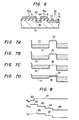
- Figure 6 illustrates the sectional structure of the memory cell and the applied voltage.
- This memory cell is not much different from the word gate driving system described in its cross-sectional structure already, and the difference is that unlike the system described already, the plate electrode 62 forming the charge storage portion is independent for each row and is disposed in parallel with the word line gate 63.
- Figures 7A, 7B, 7C and 7D illustrate the principle of discriminating the storage states of the multi-level charge in accordance with this system.
- a low voltage 80 is applied to the word line 5 in order to prevent the leakage of the charge 70 of the storage portion to the bit line during holding of the charge and to sufficiently raise the potential barrier (72) below the word line gate.
- a voltage 81 which is higher than that during data holding is applied to the selected row to reduce the potential barrier (74, 76, 78) below the word line gate so that the charge flowing out from the storing portion is caused to flow only through the bit line.
- Figures 9A through 9E illustrate the potential along the surface of the semiconductor layer of the memory cell during the storing operating
- Figure 10 illustrates the voltage waveform at each portion of the memory cell when the storing operating is conducted.
- the potential 92 of the bit line is set-to a level somewhat lower than the potential barrier (91) below the word line gate in the selected state before the storing operation is effected.
- Multi-level step voltage ⁇ pL (103 - 106) which changes from a low voltage to the high is applied to the plate.
- the potential well below the plate is thus made deeper gradually (90, 93, 97, 99).
- a pulse 108 in a negative direction is applied to the bit line while the multi-level step voltage ⁇ p L keeps a constant value 105, as shown in Fugure 10.
- the mode 94 of injection of the charge 95 in this case is shown in Figure 9C.
- the amount of charge 96 determined by the potential barrier 91 below the word line gate and the depth of the potential well below the plate can be stored inside the potential well ( Figure 9D) by returning the drain voltage to the value 107 during the same period.
- Figure 9E illustrates the charge storage state. (The word line voltage is reduced; 101 + 102.)
- Figure 11 illustrates an example of a memory using a multi-level storage structure in which a memory cell of the word gate driving system is used as each unit memory.
- a memory cell is shown constituted by n-channel MOS-FET 115 and a charge storing portion 116.
- Reference numeral 111 represents a row address select circuit, which selects only one row from a plurality of rows.
- a predetermined voltage is applied from the row address select circuit to the gate of a row address select transistor 109, which is connected to the word line 117, so as to render the transistor 109 conductive.
- Reference numeral 113 represents a multi-level step voltage generator, and the output of this generator is connected to the word line 117 through the transistor 109.
- the multi-level step generator 113 is driven by a triggering pulse ⁇ 15C.
- a high sensitive sense amplifier 120 is connected to one of the ends of a bit line 118.
- This amplifier consists of a pre-sense circuit which amplifies a minute change of the bit line potential by voltage amplification or the like, and a main sense circuit which amplifies the output of the pre-sense circuit to a logic swing inside the memory, and drives level storage cells consisting of n-channel MOS-FETs.
- the output line 133 is discharged from the power source potential V cc to the ground potential V ss at the time at which a signal is detected on the bit line.
- Eight transistors 121 through 128 constitute 4-level temporary storage cells. Two transistors store one level.
- this embodiment can discriminate and read four levels of charge storage state (2 bits).
- two signal lines for one level (or 8 signal lines in all) are disposed so as to cross the output line of the amplifier described above.
- Four lines 129 through 132 are read signal lines which operate at the time of data read, while the lines 134 through 137 are write signal lines which operate at the time of data storage, respectively.
- the read signal lines are connected to a read reference signal generator 114.
- a shift register is used as the read reference signal generator, which produces the power source voltage V cc in the time sequence of 129 - 132 in synchronism with the multi-level step voltage under the control of the triggering pulse 150.
- the logic data of the read signal lines 129 through 132 are temporarily stored as the potentials of the gate terminals of the transistors 122, 124, 126 and 128. In this manner, the mutually different multi-level charge data produced from the memory cells aligned on the same row to the respective data lines are temporarily held as the logic swing data stored in the 4-level temporary storage cells connected to the respective bit lines.
- Figure 12 illustrates the voltage waveform at each portion corresponding to the read operation.
- Figures 12(a) through 12(d) illustrate the triggering pulse ⁇ , the word line potential ⁇ R , the bit line potential, and the output voltage of the sense amplifier, respectively.
- Figures 12(e) through 12(h) illustrate the voltage of read reference signal lines.
- Figures 12(i) through 12(1) illustrate the gate potentials of the transistors 122, 124, 126 and 128 of the temporary storage cells, respectively.
- a potential 217 which is lower by the threshold voltage of the gate of the transistor 123 than the power source voltage V cc is temporarily held at the gate of the transistor 124, making the transistor 124 conductive.
- Figure 14 illustrates the potential along the memory cell section corresponding to the read operation of the 4-level charge storage state shown in this embodi - ment.
- the potential barriers below the word line gate corresponding to the word line voltages ( ⁇ R ) 201, 202, 203 and 204 are represented by 401, 402, 403 and 404, respectively.
- ⁇ R When the word line voltage ⁇ R is discharged from 401 to 402, the flow-out of charge occurs when the surface potential of the charge storing portion is higher than 411, whereby the amplifier 120 operates and a voltage lower by the threshold voltage of the transistor 121 than V cc is stored at the gate of the transistor 122.
- the flow-out of charge occurs when the surface potential of the charge storing portion is within the potential range of between 411 and 412 and between 412 and 413, and the potentials lower by the threshold voltage than V cc are stored at the gates of the transistors 124 and 126, respectively.
- the potential of the output line 133 of the amplifier is reduced so as to store a potential, which is lower by the threshold voltage than V , at the gate of the transistor 128 in synchronism with the voltage pulse 212.
- the information in which of the four ranges 420, 421, 422 and 423 in Figure 4 the surface potential of the storage portion is positioned, is transferred to the data of the temporary storage cells outside the memory cell array. These four levels can be made to correspond to the digital binary signals (1, 1), (1, 0), (0, 1) and (0, 0), respectively.
- a reset pulse s is applied to a line 162, and each data line 118 is reduced to V ss (base potential) through MOS-FET 140.
- the signal generator 151 operates in synchronism with the triggering pulse ⁇ .
- This embodiment uses a shift register as the write signal generator, which produces in a time sequence a power source potential V cc from 134 to 137 in synchronism with the multi-level step voltage ⁇ R .
- the temporary storage cell output line 138 is connected to the write signal line 136 through the transistor 124 storing temporarily V cc at its gate.
- V cc is produced to the temporary storage cell output line 138 for the first time when the write signal line 136 reaches V cc .
- cc the logic data corresponding to the 4- level voltages stored temporarily in the temporary storage cells and the 4-level logic data of the write signal lines are compared, and only when they are in agreement with one another, the temporary storage cell output line 138 shifts to the high logic level, rendering the write transistor 141 conductive through the buffer 139 and raising the potential of the bit line 118 (rises to V cc )
- the charge corresponding to the potential barrier below the 4-level word line gate is thus left in the charge storage portion, and the write operation is completed.
- this embodiment represents that the rewriting operation (refresh operation) which is essential in a charge storage type semiconductor memory can be accomplished easily.
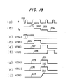
- Figure 13 illustrates the voltage waveform at each portion during the writing operation.
- Figures 13(a) and 13(b) illustrate the waveforms of the triggering pulse and the word line potential ⁇ R , respectively
- Figures 13(c) through 13(f) illustrate the waveforms of the potentials of the write reference signal lines 134 through 137, respectively
- Figure 13(g) illustrates the waveform of the potential of the temporary storage cell output line 138
- Figure 13(i) does the waveform of the bit line potential 118.
- a column address select circuit 112 is further added.
- a transistor 142 is connected to the output line of the 4-level temporary storage cell 138 selected by the select circuit 112 and to a common data line 143. Therefore, when the output line of the temporary storage cell 138 shifts to V cc during the writing operation, the common data line 143 shifts simultaneously to V cc ( Figure 13(h)).
- a 4-level to 2-bit encoder ENC is disposed inside an interface circuit. This encoder ENC produces the 4-level logic data appearing on the write signal lines 134 - 137 in synchronism with the shift of the common data line 143 to the high level as the 2-bit binary signals to input-output terminals 145 and 146.
- This rewriting operation is conducted only for the column which is selected by the column address select circuit 112.
- the output line of the amplifier 133 for the selected column is discharged to V ss by a write enable signal ⁇ WE through the transistor 149. Accordingly, the data thus read out are not held in the temporary storage cells.
- the digital binary signals corresponding to the rewrite data that are applied from outside through the terminals 145 and 146 are decoded by a decoder DEC disposed inside the interface circuit 144, and shift one of the output lines of the decoder 163 - 166 to V cc and the rest, to V .
- V cc is produced in the time sequence to the four write signal lines 134 through 137 in the same way as in the rewriting mode in the refresh cycle described already, and the signal and the previous decoder output signals are compared with each other, so that the common data line 143 is changed from V ss to V cc at the timing at which both signals coincide with each other (see Figure 15).
- EOR is an exclusive-OR circuit (EOR gate) and NOR is an inversion logic summation circuit (NOR gate).
- This signal is transmitted to the output line 138 of the temporary storage cells through the transistor 142 to actuate the write transistor 141.
- the 2-bit digital signal applied from outside the semiconductor memory can be written as a 4-level voltage state into a memory cell positioned at the point of intersection of one row address line and one column address line.
- Figure 16 illustrates an example of a semiconductor memory using the multiple level storage structure, which uses plate driving type memory cells as the unit memory cells.
- an n-channel MOS-FET 115 and a MOS type charge storing portion 175 constitute a memory'cell.
- a first row address select line (word line) 173 is connected to the gate of MOS-FET of the memory cell, while a second row address select line 174 is connected to the electrode (plate) of the MOS charge storage portion 175.
- the first and second row select lines that are parallel to each other are connected to a potential application line ⁇ WR 170 of the word line and to the output line 0 R 119 of the multi-level step wave through the row address select transistors 171 and 172, respectively.
- the row address select transistors 171 and 172 are simultaneously selected by the row address select circuit 11.
- the constructions other than the write circuit are the same as those of the embodiment 1 described already.
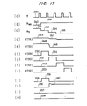
- Figure 17 illustrates the voltage waveform at each portion during the read mode.
- the process in which the charge flows onto the data lines by ⁇ WR and ⁇ R has been described in detail in the foregoing "Summary of the Invention".
- the other processes of the read mode are the same as those of the Embodiment 1 and are therefore omitted.
- Figure 18 illustrates the voltage waveform at each portion during the write mode.
- the output line 138 of the temporary storage memory cells actuates the pulse generator 176 (in Figure 16) so as to generate a potential change such as shown in Figure 18(j). Since the other operations are the same as those of the Embodiment 1, their description is hereby omitted.
Abstract
Description
- This invention relates to a semiconductor memory, and more particularly to a semiconductor integrated .circuit memory.
- As typified by a dynamic random access memory (DRAM) or a semiconductor memory using a charge coupled device (CCD memory), a semiconductor memory having a high integration density stores data by making the existence and absence of charge inside a potential well on a semiconductor surface correspond to digital signals "1" and "0".
- However, this storing method involves the problem that in the case of DRAM, for example, only binary 1- digit (1-bit) data can be handled for each unit memory cell, and hence the amount of total bits per chip is limited.
- Particularly in the charge storage type memory such as described above, charge leaks from a pn junction formed essentially in a charge storage portion so that the data can be stored only for a limited period of time. This results in another problem that a mechanism for rewriting (refreshing) the stored data on a certain cycle of time within that period is essentially necessary.
- The CCD memory has a structure in which the stored charge is cycled using a transfer electrode. In order to effect rewrite (refresh), therefore, the stored charge is transferred along a CCD transfer electrode loop arranged cyclicly, and the charge must be read and written at an input-output portion disposed at a predetermined position inside the CCD loop on a certain cycle-of time. However, a great deal of power is necessary to charge and discharge the transfer electrodes for transferring the charge in order to refresh all data, and it has therefore been difficult in the past to provide a memory having low power consumption.
- Semiconductor memories having higher integration density as exemplified by a semiconductor dynamic random access memory (hereinafter called "DRAM") have been developed every year, and miniaturization of unit memory cells (hereinafter called "memory cells") of the semiconductor memory and its peripheral circuits is ever-increasing. In order to improve the integration density by miniaturization such as described above, however, a drastic improvement must be made in device process technique such as photolithography, etching and the like, but a considerably long period of time is generally necessary before improved device process technique is developed.
- In contrast, demands for very high integration density semiconductor memories are ever-increasing, and semiconductor memories having low power consumption are earnestly required in a novel field of application such as miniature computers for office use and their peripheral terminals that have been made a remarkable progress in recent years. For these reasons, existing semiconductors are not entirely satisfactory not only in.their integration density but also in their performance such as power consumption.
- To fulfill the demands described above, semiconductor memories using multiple level storage structure (MLS memories) are believed to be effective means that can realize very high integration density semiconductor memories and are available in accordance with the existing process technique. The memory improves substantially the integration density by storing data of at least more than two levels per memory cell.
- A multi-level storage memory using charge coupled device (hereinafter called "CCD") has been known in the past. The memory is described in detail in L. Terman et al. IEEE Journal of Solid-State Circuits, Vol. sc-16, No. 5, pp. 472 - 478, October, 1981, and M. Yamada et al, Proceedings of the 9th Conference on Solid-State Devices, Tokyo,1977, pp. 263 - 268, issued on January, 1978, for example.
- However, the multi-level storage memory using the charge coupled devices (CCD) has not much been put into practical application for the following reasons.
- (1) Since signal charge transfer inefficiency is not zero in CCD, analog signal charge corresponding to multi-level data damps with the charge transfer, and hence the number of multi-level can not be increased so much.
- (2) The amplitude of a driving pulse must be increased in order to improve the signal charge transfer efficiency, and this results in extremely great power consumption in addition to the inherent property of the cell that it has originally large capacitance load.
- (3) Since A/D and D/A convertors having high accuracy are necessary for each CCD loop, the integration density can not be increased due to the limitation of peripheral circuits, even if the memory cell can be miniaturized.
- The present invention is therefore directed to provide a multi-level storage semiconductor memory (MLS memory) which eliminates the problems described above and can simultaneously accomplish low power consumption and large memory capacity. The present invention realizes a very high integration density MLS memory by introducing a novel concept that has not been known in the past.
- It is another object of the present invention to provide a multi-level storage semiconductor memory using addressing by both rows and columns.
- Since the present invention employs addressing by both rows and columns for the construction of the MLS memory, the present invention can provide a large capacity memory which has low power consumption but can select at random memory cells.
- The present invention introduces an entirely novel concept that a multi-level step voltage is applied to a word line or a plate so as to read the data at the timing at which stored charge flows out, and writes the data to the memory cell at the timing which corresponds to an input signal. The present invention can realize efficiently a very high density semiconductor memory on the basis of this novel concept.
-
- Figure 1 is a sectional view of a memory cell of a word line driving system;
- Figures 2A through 2C are schematic views showing the potential with respect to electrons along the surface of a semiconductor layer in the read mode of the memory cell of the word line driving system;
- Figure 3 is a diagram showing the change of a word line voltage and a bit line voltage in the read mode of the memory cell of the word line driving system;
- Figures 4A through 4D are schematic views showing the potential with respect to electrons along the surface of a semiconductor layer in the write mode of the memory cell of the word line driving system;
- Figure 5 is a diagram showing the change of a word line voltage and a bit line voltage in the write mode of the memory cell of the word line driving system;
- Figure 6 is a sectional view of a memory cell of a plate driving system;
- Figures 7A.through 7D are schematic views showing the potential with respect to electrons along the surface of a semiconductor layer in the read mode of the memory cell of the plate driving system;
- Figure 8 is a diagram showing the change of a word line potential, a plate voltage and a bit line voltage in the read mode of the memory cell of the plate driving system;
- Figures 9A through 9E are schematic views showing the potential along the surface of a semiconductor layer in the write mode of the memory cell of the plate driving system;
- Figure 10 is a diagram showing the change of a word line voltage, a plate voltage and a bit line voltage in the memory cell of the plate driving system;
- Figure 11 is a circuit diagram showing a memory array, a read circuit and a write circuit of a semiconductor memory using a memory cell of a word line driving system;
- Figure 12 is a pulse chart showing the voltage waveform at each portion in the read mode of the semiconductor memory shown in Figure 11;
- Figure 13 is a pulse chart showing the voltage waveform at each portion in the write mode of the semiconductor memory shown in Figure 11;
- Figure 14 is a diagram showing the surface potential of the memory cell and useful for explaining the read of 4-level charge storage state;
- Figure 15 is a circuit diagram showing an interface circuit of the semiconductor memory shown in Figure 11;
- Figure 16 is a circuit diagram showing a memory array, read circuit and write circuit of a semiconductor memory using a plate driving system;
- Figure 17 is a pulse chart showing the voltage waveform at each portion in the read mode of the semiconductor memory shown in Figure 16; and
- Figure 18 is a pulse chart showing the voltage waveform at each portion in the write mode of the semiconductor memory shown in Figure 16.
- First of all, the principle of the reading and storing operations of the multi-level (three or more levels) charge storage state as the basis of the MLS memory of the present invention will be described.
- Figure 1 illustrates the sectional structure of a memory cell in accordance with the first principle of the invention and the kind of applied voltages. For convenience' sake, the memory based on the later- appearing principle will be hereinafter called a "word gate driving MLS memory". Although the electron is dealt with as the stored charge, the principle can be applied exactly in the same way to the positive hole by converting the conductivity type of a semiconductor and inverting the voltage for operating the memory.
- In the drawing,
reference numeral 10 represents a p-type semiconductor layer (a substrate of a semiconductor layer disposed on the substrate), reference numeral 11 is a gate insulating film (oxidized film or the like), andreference numerals Reference numerals electrode 13 corresponds to the gate of an insulated gate field effect transistor (MOS-FET), and the n-type semiconductor layers plate electrode 12, an inversion layer which is induced on the surface of the semiconductor layer 1O is electrically coupled with the n-type semiconductor layer 15, thereby forming a capacitance in cooperation with theelectrode 12 and making it possible to store the electrons in the inversion layer. When this memory cell is used in a memory device consisting of a two-dimensional arragnement, thegate 13 of MOS-FET is connected to an address decoded row line (word line) 2, and thedrain 14, to an address decoded column line (bit line) 3 to form a memory matrix.Theelectrode 12 is connected in common to all the memory cells, and a positive D.C. voltage is applied to it. - Figures 2A, 2B and 2C illustrate the surface potential to the electrons along the surface of the semiconductor layer of the memory cell shown in Figure 1. Figure 2A illustrates the charge storage mode. The
stored charge 20 in thepotential well 21 below the plate is isolated from thebit line 23 by apotential barrier 22 below the gate of MOS-FET, and from the other regions by the potential barrier of an isolation region disposed around the memory cell. When read of the multi-level charge state is effected, multi-level step voltages φw (30, 31, 32) that shifts from a low voltage to a high voltage are applied to the word line.2 as shown in Fig. 3. In the drawing, reference numeral 30 corresponds to Figure 2A, 31 to Figure 2B, and 32 to Figure 2C. When the voltage øw is increased in a positive direction, the potential barrier below the gate of MOS-FET drops in the sequence of 22 → 24 → 26 as shown in Figures 2A, 2B and 2C, and when it becomes below the surface potential at a storage node 25 (the state represented by 26), the charge flows out (27) from the storage portion to the bit line. Figure 3 illustrates the mode of drop of the bit line voltage VD (33, 34) caused by the outflow of the charge. - As described above, the storage state of the charge having three or more levels can be discriminated by detecting the timing at which the difference between the potential barrier below the gate of the word line and the potential at the storage portion, when the former is gradually reduced, is inverted, as the change of the bit line voltage VD.
- Next, the principle of the writing mode of the multi-level charge storage state will be described. Figures 4A through 4D are schematic views showing the concept of the potential on the surface of the semiconductor layer when the multi-level charge is stored, and Figure 5 shows the change, with time, of the word line and bit line.voltages when charge storage is effected. Figures 4A through 4D correspond to the state of application of the voltages represented by
reference numerals 50 through 53 in Figure 5, respectively. Before writing is executed, the word line applied voltage φw is set in advance to the highest level so that the potential barrier below' the gate of the word line becomes minimal (42), while the data line voltage VD is set in advance to thelowest level 54 at which thepotential well 41 of the storage portion is sulfilled by the charge 42 (for example, to the ground potential). Next, the multi-level step voltage øw (50 - 53) shown in Figure 5 is applied to the word line. Then, the bit line voltage VD is raised from 54 to 55 as shown in Figure 5 at the timing at which the potential barrier (43, 45, 48) below the gate of the word line is in agreement with the surface potential which corresponds to the amount of charge to be stored finally, and the charge is extracted (44) from thebit line 46 as shown in Figure 4C. Figure 4D shows the final charge storage state (stored charge 47). - Next, the reading and storing operation of the multi-level (two or more levels) charge storage state in the memory cell in accordance with the second principle will be described. Hereinafter, this principle will be called a "plate electrode driving MLS memory" to distinguish it. from the word gate driving system described earlier for convenience' sake.
- Figure 6 illustrates the sectional structure of the memory cell and the applied voltage. This memory cell is not much different from the word gate driving system described in its cross-sectional structure already, and the difference is that unlike the system described already, the
plate electrode 62 forming the charge storage portion is independent for each row and is disposed in parallel with theword line gate 63. - Figures 7A, 7B, 7C and 7D illustrate the principle of discriminating the storage states of the multi-level charge in accordance with this system. A
low voltage 80 is applied to theword line 5 in order to prevent the leakage of thecharge 70 of the storage portion to the bit line during holding of the charge and to sufficiently raise the potential barrier (72) below the word line gate. During the read operation, avoltage 81 which is higher than that during data holding is applied to the selected row to reduce the potential barrier (74, 76, 78) below the word line gate so that the charge flowing out from the storing portion is caused to flow only through the bit line. Under this selected state, when the voltage φPL of the second row address line (plate) 62 disposed in parallel with the word line is decreased gradually and step-wise (82 - 85) as shown in Figure 8, the depth of the potential well on the surface of the semiconductor layer becomes smaller in response to the potential (71 → 73 → 75 → 77), and the surface potential rises. Figures 7B through 7D illustrate this state. When the surface potential at the storage node becomes higher than the potential barrier below the word line gate that is set previously, the flow ofcharge 79 to the bit line such as shown in Figure 7D occurs. Thus, the charge storage state of the multi-level (two or more levels) can be discriminated by detecting the timing of the change of the bit line voltage VD (change of 86 + 87 in Figure 8) in the same way as in the word gate driving system. - Likewise, the principle of the writing operation of the storage state of the multi-level (two or more levels) charge in this plate electrode driving system will be described. Figures 9A through 9E illustrate the potential along the surface of the semiconductor layer of the memory cell during the storing operating, and Figure 10 illustrates the voltage waveform at each portion of the memory cell when the storing operating is conducted.
- The potential 92 of the bit line is set-to a level somewhat lower than the potential barrier (91) below the word line gate in the selected state before the storing operation is effected. Multi-level step voltage φpL (103 - 106) which changes from a low voltage to the high is applied to the plate. The potential well below the plate is thus made deeper gradually (90, 93, 97, 99). When a
voltage 104 shown in Figure 10 is applied to the plate, the potential well occurs as shown in Figure 9B, but the charge is not injected. To effect the writing operation, apulse 108 in a negative direction is applied to the bit line while the multi-level step voltage ØpL keeps aconstant value 105, as shown inFugure 10. Themode 94 of injection of thecharge 95 in this case is shown in Figure 9C. The amount ofcharge 96 determined by thepotential barrier 91 below the word line gate and the depth of the potential well below the plate can be stored inside the potential well (Figure 9D) by returning the drain voltage to thevalue 107 during the same period. - Figure 9E illustrates the charge storage state. (The word line voltage is reduced; 101 + 102.)
- Hereinafter, three embodiments of the invention will be described.
- Figure 11 illustrates an example of a memory using a multi-level storage structure in which a memory cell of the word gate driving system is used as each unit memory. In the drawing, a memory cell is shown constituted by n-channel MOS-
FET 115 and a charge storing portion 116.Reference numeral 111 represents a row address select circuit, which selects only one row from a plurality of rows. In order to select aword line 117, a predetermined voltage is applied from the row address select circuit to the gate of a row address select transistor 109, which is connected to theword line 117, so as to render the transistor 109 conductive. In the case of the n-channel MOS transistor shown in this embodiment, a power source voltage V cc or a voltage higher than the former is applied to the gate.Reference numeral 113 represents a multi-level step voltage generator, and the output of this generator is connected to theword line 117 through the transistor 109. Themulti-level step generator 113 is driven by a triggering pulse Φ15C. - On the other hand, a high
sensitive sense amplifier 120 is connected to one of the ends of abit line 118. This amplifier consists of a pre-sense circuit which amplifies a minute change of the bit line potential by voltage amplification or the like, and a main sense circuit which amplifies the output of the pre-sense circuit to a logic swing inside the memory, and drives level storage cells consisting of n-channel MOS-FETs. In this embodiment, theoutput line 133 is discharged from the power source potential V cc to the ground potential Vss at the time at which a signal is detected on the bit line. Eighttransistors 121 through 128 constitute 4-level temporary storage cells. Two transistors store one level. Accordingly, this embodiment can discriminate and read four levels of charge storage state (2 bits). In the 4-level temporary storage cells, two signal lines for one level (or 8 signal lines in all) are disposed so as to cross the output line of the amplifier described above. Fourlines 129 through 132 are read signal lines which operate at the time of data read, while thelines 134 through 137 are write signal lines which operate at the time of data storage, respectively. The read signal lines are connected to a readreference signal generator 114. In this embodiment, a shift register is used as the read reference signal generator, which produces the power source voltage V cc in the time sequence of 129 - 132 in synchronism with the multi-level step voltage under the control of the triggeringpulse 150. - When the
output line 133 of the amplifier is set in advance to Vcc and when it is discharged to the ground potential Vss at the timing of the flow-out of the charge, the logic data of theread signal lines 129 through 132 are temporarily stored as the potentials of the gate terminals of thetransistors - Figure 12 illustrates the voltage waveform at each portion corresponding to the read operation. Figures 12(a) through 12(d) illustrate the triggering pulse ø, the word line potential φR, the bit line potential, and the output voltage of the sense amplifier, respectively. Figures 12(e) through 12(h) illustrate the voltage of read reference signal lines.
- Figures 12(i) through 12(1) illustrate the gate potentials of the
transistors transistor 123 than the power source voltage Vcc is temporarily held at the gate of thetransistor 124, making thetransistor 124 conductive. - Figure 14 illustrates the potential along the memory cell section corresponding to the read operation of the 4-level charge storage state shown in this embodi- ment. The potential barriers below the word line gate corresponding to the word line voltages (φR) 201, 202, 203 and 204 are represented by 401, 402, 403 and 404, respectively. When the word line voltage φR is discharged from 401 to 402, the flow-out of charge occurs when the surface potential of the charge storing portion is higher than 411, whereby the
amplifier 120 operates and a voltage lower by the threshold voltage of thetransistor 121 than V cc is stored at the gate of thetransistor 122. Similarly, with the drop of the voltage φR from 202 + 203, 203 + 204, the flow-out of charge occurs when the surface potential of the charge storing portion is within the potential range of between 411 and 412 and between 412 and 413, and the potentials lower by the threshold voltage than Vcc are stored at the gates of thetransistors - If the surface potential of the charge storage portion is below 413, the flow-out charge does not occur to the end. In such a case, the potential of the
output line 133 of the amplifier is reduced so as to store a potential, which is lower by the threshold voltage than V , at the gate of thetransistor 128 in synchronism with thevoltage pulse 212. When the operation described above is carried out, the information, in which of the four ranges 420, 421, 422 and 423 in Figure 4 the surface potential of the storage portion is positioned, is transferred to the data of the temporary storage cells outside the memory cell array. These four levels can be made to correspond to the digital binary signals (1, 1), (1, 0), (0, 1) and (0, 0), respectively. - Next, the operation at the time of charge storage (writing) will be explained. First, a reset pulse s is applied to a line 162, and each
data line 118 is reduced to Vss (base potential) through MOS-FET 140. Then, thesignal generator 151 operates in synchronism with the triggering pulse ø. This embodiment uses a shift register as the write signal generator, which produces in a time sequence a power source potential Vcc from 134 to 137 in synchronism with the multi-level step voltage φR. On the other hand, the temporary storagecell output line 138 is connected to thewrite signal line 136 through thetransistor 124 storing temporarily Vcc at its gate. Accordingly, V cc is produced to the temporary storagecell output line 138 for the first time when thewrite signal line 136 reaches Vcc. cc In other words, the logic data corresponding to the 4- level voltages stored temporarily in the temporary storage cells and the 4-level logic data of the write signal lines are compared, and only when they are in agreement with one another, the temporary storagecell output line 138 shifts to the high logic level, rendering thewrite transistor 141 conductive through thebuffer 139 and raising the potential of the bit line 118 (rises to Vcc) As already described generally, the charge corresponding to the potential barrier below the 4-level word line gate is thus left in the charge storage portion, and the write operation is completed. - As described above, this embodiment represents that the rewriting operation (refresh operation) which is essential in a charge storage type semiconductor memory can be accomplished easily.
- Figure 13 illustrates the voltage waveform at each portion during the writing operation. Figures 13(a) and 13(b) illustrate the waveforms of the triggering pulse and the word line potential φR, respectively, Figures 13(c) through 13(f) illustrate the waveforms of the potentials of the write
reference signal lines 134 through 137, respectively, Figure 13(g) illustrates the waveform of the potential of the temporary storagecell output line 138, and Figure 13(i) does the waveform of thebit line potential 118. - To produce the read data outside the semiconductor memory, a column address
select circuit 112 is further added. A transistor 142 is connected to the output line of the 4-leveltemporary storage cell 138 selected by theselect circuit 112 and to acommon data line 143. Therefore, when the output line of thetemporary storage cell 138 shifts to Vcc during the writing operation, thecommon data line 143 shifts simultaneously to V cc (Figure 13(h)). As shown in Figure 15, a 4-level to 2-bit encoder ENC is disposed inside an interface circuit. This encoder ENC produces the 4-level logic data appearing on the write signal lines 134 - 137 in synchronism with the shift of thecommon data line 143 to the high level as the 2-bit binary signals to input-output terminals - Next, the rewriting operation of the stored data will be described. This rewriting operation is conducted only for the column which is selected by the column address
select circuit 112. When the rewriting operation is made, it is necessary to make the temporary storage cells inactive before the start of the rewriting operation. For this purpose, the output line of theamplifier 133 for the selected column is discharged to Vss by a write enable signal φWE through thetransistor 149. Accordingly, the data thus read out are not held in the temporary storage cells. - The digital binary signals corresponding to the rewrite data that are applied from outside through the
terminals interface circuit 144, and shift one of the output lines of the decoder 163 - 166 to Vcc and the rest, to V . On the other hand, Vcc is produced in the time sequence to the fourwrite signal lines 134 through 137 in the same way as in the rewriting mode in the refresh cycle described already, and the signal and the previous decoder output signals are compared with each other, so that thecommon data line 143 is changed from Vss to V cc at the timing at which both signals coincide with each other (see Figure 15). - In Figure 15, EOR is an exclusive-OR circuit (EOR gate) and NOR is an inversion logic summation circuit (NOR gate). This signal is transmitted to the
output line 138 of the temporary storage cells through the transistor 142 to actuate thewrite transistor 141. As a result of the operation described above, the 2-bit digital signal applied from outside the semiconductor memory can be written as a 4-level voltage state into a memory cell positioned at the point of intersection of one row address line and one column address line. - Figure 16 illustrates an example of a semiconductor memory using the multiple level storage structure, which uses plate driving type memory cells as the unit memory cells. In the drawing, an n-channel MOS-
FET 115 and a MOS type charge storing portion 175 constitute a memory'cell. A first row address select line (word line) 173 is connected to the gate of MOS-FET of the memory cell, while a second row addressselect line 174 is connected to the electrode (plate) of the MOS charge storage portion 175. The first and second row select lines that are parallel to each other are connected to a potentialapplication line φ WR 170 of the word line and to the output line 0R 119 of the multi-level step wave through the row addressselect transistors 171 and 172, respectively. The row addressselect transistors 171 and 172 are simultaneously selected by the row address select circuit 11. The constructions other than the write circuit are the same as those of the embodiment 1 described already. - Figure 17 illustrates the voltage waveform at each portion during the read mode. The process in which the charge flows onto the data lines by φWR and ØR has been described in detail in the foregoing "Summary of the Invention". The other processes of the read mode are the same as those of the Embodiment 1 and are therefore omitted.
- Figure 18 illustrates the voltage waveform at each portion during the write mode. In the write mode, the
output line 138 of the temporary storage memory cells actuates the pulse generator 176 (in Figure 16) so as to generate a potential change such as shown in Figure 18(j). Since the other operations are the same as those of the Embodiment 1, their description is hereby omitted.
Claims (11)
Applications Claiming Priority (2)
| Application Number | Priority Date | Filing Date | Title |
|---|---|---|---|
| JP58120364A JPS6013398A (en) | 1983-07-04 | 1983-07-04 | Semiconductor multi-value storage device |
| JP120364/83 | 1983-07-04 |
Publications (3)
| Publication Number | Publication Date |
|---|---|
| EP0130614A2 true EP0130614A2 (en) | 1985-01-09 |
| EP0130614A3 EP0130614A3 (en) | 1988-08-31 |
| EP0130614B1 EP0130614B1 (en) | 1992-03-11 |
Family
ID=14784365
Family Applications (1)
| Application Number | Title | Priority Date | Filing Date |
|---|---|---|---|
| EP84107724A Expired EP0130614B1 (en) | 1983-07-04 | 1984-07-03 | Semiconductor memory using multiple level storage structure |
Country Status (6)
| Country | Link |
|---|---|
| US (1) | US4709350A (en) |
| EP (1) | EP0130614B1 (en) |
| JP (1) | JPS6013398A (en) |
| KR (1) | KR920001074B1 (en) |
| CA (1) | CA1224567A (en) |
| DE (1) | DE3485555D1 (en) |
Cited By (8)
| Publication number | Priority date | Publication date | Assignee | Title |
|---|---|---|---|---|
| EP0148488A2 (en) * | 1983-12-23 | 1985-07-17 | Hitachi, Ltd. | Semiconductor memory having multiple level storage structure |
| WO1992012518A1 (en) * | 1991-01-09 | 1992-07-23 | Siemens Aktiengesellschaft | Storage cell arrangement and process for operating it |
| WO1995020225A1 (en) * | 1994-01-21 | 1995-07-27 | Intel Corporation | Method and circuitry for storing discrete amounts of charge in a single memory element |
| US5677869A (en) * | 1995-12-14 | 1997-10-14 | Intel Corporation | Programming flash memory using strict ordering of states |
| US5701266A (en) * | 1995-12-14 | 1997-12-23 | Intel Corporation | Programming flash memory using distributed learning methods |
| US5729489A (en) * | 1995-12-14 | 1998-03-17 | Intel Corporation | Programming flash memory using predictive learning methods |
| US5737265A (en) * | 1995-12-14 | 1998-04-07 | Intel Corporation | Programming flash memory using data stream analysis |
| US5748546A (en) * | 1994-06-02 | 1998-05-05 | Intel Corporation | Sensing scheme for flash memory with multilevel cells |
Families Citing this family (19)
| Publication number | Priority date | Publication date | Assignee | Title |
|---|---|---|---|---|
| FR2580421A1 (en) * | 1985-04-12 | 1986-10-17 | Eurotechnique Sa | ELECTRICALLY PROGRAMMABLE DEAD MEMORY |
| JP2678062B2 (en) * | 1989-06-14 | 1997-11-17 | キヤノン株式会社 | Photoelectric conversion device |
| US5218569A (en) | 1991-02-08 | 1993-06-08 | Banks Gerald J | Electrically alterable non-volatile memory with n-bits per memory cell |
| US6002614A (en) | 1991-02-08 | 1999-12-14 | Btg International Inc. | Memory apparatus including programmable non-volatile multi-bit memory cell, and apparatus and method for demarcating memory states of the cell |
| JP2921812B2 (en) * | 1992-12-24 | 1999-07-19 | シャープ株式会社 | Nonvolatile semiconductor memory device |
| US5515317A (en) * | 1994-06-02 | 1996-05-07 | Intel Corporation | Addressing modes for a dynamic single bit per cell to multiple bit per cell memory |
| US6353554B1 (en) | 1995-02-27 | 2002-03-05 | Btg International Inc. | Memory apparatus including programmable non-volatile multi-bit memory cell, and apparatus and method for demarcating memory states of the cell |
| US5815434A (en) * | 1995-09-29 | 1998-09-29 | Intel Corporation | Multiple writes per a single erase for a nonvolatile memory |
| JP3613622B2 (en) * | 1996-09-27 | 2005-01-26 | 株式会社日立製作所 | Semiconductor memory |
| US5761114A (en) * | 1997-02-19 | 1998-06-02 | International Business Machines Corporation | Multi-level storage gain cell with stepline |
| JPH11178383A (en) * | 1997-12-04 | 1999-07-02 | Toshiba Corp | Motor controller |
| US6279133B1 (en) | 1997-12-31 | 2001-08-21 | Kawasaki Steel Corporation | Method and apparatus for significantly improving the reliability of multilevel memory architecture |
| JP2000116199A (en) | 1998-10-01 | 2000-04-21 | Toshiba Corp | Controller for motor |
| KR20030003312A (en) * | 2001-06-30 | 2003-01-10 | 주식회사 하이닉스반도체 | Semiconductor device with multiple bit capacitor |
| JP2009009641A (en) * | 2007-06-27 | 2009-01-15 | Elpida Memory Inc | Semiconductor memory and read method thereof |
| WO2009061532A1 (en) * | 2007-11-08 | 2009-05-14 | Rambus Inc. | Voltage-stepped low-power memory device |
| US8773925B2 (en) | 2010-02-23 | 2014-07-08 | Rambus Inc. | Multilevel DRAM |
| WO2011114905A1 (en) * | 2010-03-19 | 2011-09-22 | Semiconductor Energy Laboratory Co., Ltd. | Semiconductor memory device |
| US10985162B2 (en) | 2018-12-14 | 2021-04-20 | John Bennett | System for accurate multiple level gain cells |
Citations (2)
| Publication number | Priority date | Publication date | Assignee | Title |
|---|---|---|---|---|
| US4024512A (en) * | 1975-06-16 | 1977-05-17 | Fairchild Camera And Instrument Corporation | Line-addressable random-access memory |
| EP0031491A2 (en) * | 1979-12-27 | 1981-07-08 | International Business Machines Corporation | Sensing system for a capacitive semiconductor memory |
Family Cites Families (1)
| Publication number | Priority date | Publication date | Assignee | Title |
|---|---|---|---|---|
| US4459609A (en) * | 1981-09-14 | 1984-07-10 | International Business Machines Corporation | Charge-stabilized memory |
-
1983
- 1983-07-04 JP JP58120364A patent/JPS6013398A/en active Granted
-
1984
- 1984-07-03 EP EP84107724A patent/EP0130614B1/en not_active Expired
- 1984-07-03 KR KR1019840003829A patent/KR920001074B1/en not_active IP Right Cessation
- 1984-07-03 DE DE8484107724T patent/DE3485555D1/en not_active Expired - Lifetime
- 1984-07-04 CA CA000458113A patent/CA1224567A/en not_active Expired
- 1984-07-05 US US06/627,895 patent/US4709350A/en not_active Expired - Lifetime
Patent Citations (2)
| Publication number | Priority date | Publication date | Assignee | Title |
|---|---|---|---|---|
| US4024512A (en) * | 1975-06-16 | 1977-05-17 | Fairchild Camera And Instrument Corporation | Line-addressable random-access memory |
| EP0031491A2 (en) * | 1979-12-27 | 1981-07-08 | International Business Machines Corporation | Sensing system for a capacitive semiconductor memory |
Non-Patent Citations (1)
| Title |
|---|
| IBM TECHNICAL DISCLOSURE BULLETIN, vol. 22, no. 7, December 1979, pages 2978-2979, New York, US; L.M.TERMAN et al.: "CCD multilevel storage detection scheme" * |
Cited By (14)
| Publication number | Priority date | Publication date | Assignee | Title |
|---|---|---|---|---|
| EP0148488B1 (en) * | 1983-12-23 | 1992-03-18 | Hitachi, Ltd. | Semiconductor memory having multiple level storage structure |
| EP0148488A2 (en) * | 1983-12-23 | 1985-07-17 | Hitachi, Ltd. | Semiconductor memory having multiple level storage structure |
| WO1992012518A1 (en) * | 1991-01-09 | 1992-07-23 | Siemens Aktiengesellschaft | Storage cell arrangement and process for operating it |
| US5471417A (en) * | 1991-01-09 | 1995-11-28 | Siemens Aktiengesellschaft | Ferroelectric memory cell arrangement |
| WO1995020225A1 (en) * | 1994-01-21 | 1995-07-27 | Intel Corporation | Method and circuitry for storing discrete amounts of charge in a single memory element |
| US5566125A (en) * | 1994-01-21 | 1996-10-15 | Intel Corporation | Method and circuitry for storing discrete amounts of charge in a single memory element |
| US6091618A (en) * | 1994-01-21 | 2000-07-18 | Intel Corporation | Method and circuitry for storing discrete amounts of charge in a single memory element |
| US5892710A (en) * | 1994-01-21 | 1999-04-06 | Intel Corporation | Method and circuitry for storing discrete amounts of charge in a single memory element |
| US5748546A (en) * | 1994-06-02 | 1998-05-05 | Intel Corporation | Sensing scheme for flash memory with multilevel cells |
| US5828616A (en) * | 1994-06-02 | 1998-10-27 | Intel Corporation | Sensing scheme for flash memory with multilevel cells |
| US5677869A (en) * | 1995-12-14 | 1997-10-14 | Intel Corporation | Programming flash memory using strict ordering of states |
| US5737265A (en) * | 1995-12-14 | 1998-04-07 | Intel Corporation | Programming flash memory using data stream analysis |
| US5729489A (en) * | 1995-12-14 | 1998-03-17 | Intel Corporation | Programming flash memory using predictive learning methods |
| US5701266A (en) * | 1995-12-14 | 1997-12-23 | Intel Corporation | Programming flash memory using distributed learning methods |
Also Published As
| Publication number | Publication date |
|---|---|
| EP0130614B1 (en) | 1992-03-11 |
| US4709350A (en) | 1987-11-24 |
| KR850001612A (en) | 1985-03-30 |
| DE3485555D1 (en) | 1992-04-16 |
| JPH0557679B2 (en) | 1993-08-24 |
| KR920001074B1 (en) | 1992-02-01 |
| EP0130614A3 (en) | 1988-08-31 |
| JPS6013398A (en) | 1985-01-23 |
| CA1224567A (en) | 1987-07-21 |
Similar Documents
| Publication | Publication Date | Title |
|---|---|---|
| US4709350A (en) | Semiconductor memory using multiple level storage structure | |
| US7023721B2 (en) | Semiconductor integrated circuit device | |
| US6016268A (en) | Three transistor multi-state dynamic memory cell for embedded CMOS logic applications | |
| KR950013392B1 (en) | Semiconductor memory device and method of reading, writing and operating | |
| US7342842B2 (en) | Data storage device and refreshing method for use with such device | |
| KR100650244B1 (en) | Gated diode memory cells | |
| US7274593B2 (en) | Nonvolatile ferroelectric memory device | |
| US4725983A (en) | Nonvolatile semiconductor memory device | |
| US8035146B2 (en) | Nonvolatile ferroelectric memory device | |
| JP3781270B2 (en) | Semiconductor integrated circuit device | |
| JP2000113683A (en) | Semiconductor device | |
| US3876993A (en) | Random access memory cell | |
| KR100674105B1 (en) | Multiple valued dram | |
| US3706079A (en) | Three-line cell for random-access integrated circuit memory | |
| KR100714823B1 (en) | Mutiple valued SRAM | |
| US4484312A (en) | Dynamic random access memory device | |
| US3997883A (en) | LSI random access memory system | |
| JP2509764B2 (en) | Dynamic memory cell and dynamic memory | |
| US4308594A (en) | MOS Memory cell | |
| US3908182A (en) | Non-volatile memory cell | |
| US3781831A (en) | Read only memory utilizing floating gate transistors and method of programming | |
| US3651491A (en) | Memory device having common read/write terminals | |
| US4004285A (en) | Read-write circuitry for one transistor per bit random access memory | |
| JPH05291534A (en) | Semiconductor device having electric charge storage device | |
| JPS6342097A (en) | Multi-level logic storage circuit |
Legal Events
| Date | Code | Title | Description |
|---|---|---|---|
| PUAI | Public reference made under article 153(3) epc to a published international application that has entered the european phase |
Free format text: ORIGINAL CODE: 0009012 |
|
| AK | Designated contracting states |
Designated state(s): DE FR GB NL |
|
| 17P | Request for examination filed |
Effective date: 19841220 |
|
| PUAL | Search report despatched |
Free format text: ORIGINAL CODE: 0009013 |
|
| AK | Designated contracting states |
Kind code of ref document: A3 Designated state(s): DE FR GB NL |
|
| 17Q | First examination report despatched |
Effective date: 19900216 |
|
| GRAA | (expected) grant |
Free format text: ORIGINAL CODE: 0009210 |
|
| AK | Designated contracting states |
Kind code of ref document: B1 Designated state(s): DE FR GB NL |
|
| REF | Corresponds to: |
Ref document number: 3485555 Country of ref document: DE Date of ref document: 19920416 |
|
| ET | Fr: translation filed | ||
| PLBE | No opposition filed within time limit |
Free format text: ORIGINAL CODE: 0009261 |
|
| STAA | Information on the status of an ep patent application or granted ep patent |
Free format text: STATUS: NO OPPOSITION FILED WITHIN TIME LIMIT |
|
| 26N | No opposition filed | ||
| PGFP | Annual fee paid to national office [announced via postgrant information from national office to epo] |
Ref country code: GB Payment date: 19950623 Year of fee payment: 12 |
|
| PGFP | Annual fee paid to national office [announced via postgrant information from national office to epo] |
Ref country code: FR Payment date: 19950718 Year of fee payment: 12 |
|
| PGFP | Annual fee paid to national office [announced via postgrant information from national office to epo] |
Ref country code: NL Payment date: 19950728 Year of fee payment: 12 |
|
| PGFP | Annual fee paid to national office [announced via postgrant information from national office to epo] |
Ref country code: DE Payment date: 19950926 Year of fee payment: 12 |
|
| PG25 | Lapsed in a contracting state [announced via postgrant information from national office to epo] |
Ref country code: GB Effective date: 19960703 |
|
| PG25 | Lapsed in a contracting state [announced via postgrant information from national office to epo] |
Ref country code: NL Effective date: 19970201 |
|
| GBPC | Gb: european patent ceased through non-payment of renewal fee |
Effective date: 19960703 |
|
| PG25 | Lapsed in a contracting state [announced via postgrant information from national office to epo] |
Ref country code: FR Effective date: 19970328 |
|
| NLV4 | Nl: lapsed or anulled due to non-payment of the annual fee |
Effective date: 19970201 |
|
| PG25 | Lapsed in a contracting state [announced via postgrant information from national office to epo] |
Ref country code: DE Effective date: 19970402 |
|
| REG | Reference to a national code |
Ref country code: FR Ref legal event code: ST |