EP0140809A1 - Echo correction apparatus, particularly for a television data transmission system - Google Patents
Echo correction apparatus, particularly for a television data transmission system Download PDFInfo
- Publication number
- EP0140809A1 EP0140809A1 EP84460007A EP84460007A EP0140809A1 EP 0140809 A1 EP0140809 A1 EP 0140809A1 EP 84460007 A EP84460007 A EP 84460007A EP 84460007 A EP84460007 A EP 84460007A EP 0140809 A1 EP0140809 A1 EP 0140809A1
- Authority
- EP
- European Patent Office
- Prior art keywords
- output
- input
- transversal filter
- coefficients
- analog
- Prior art date
- Legal status (The legal status is an assumption and is not a legal conclusion. Google has not performed a legal analysis and makes no representation as to the accuracy of the status listed.)
- Granted
Links
Images

Classifications
-
- H—ELECTRICITY
- H04—ELECTRIC COMMUNICATION TECHNIQUE
- H04B—TRANSMISSION
- H04B3/00—Line transmission systems
- H04B3/02—Details
- H04B3/20—Reducing echo effects or singing; Opening or closing transmitting path; Conditioning for transmission in one direction or the other
- H04B3/23—Reducing echo effects or singing; Opening or closing transmitting path; Conditioning for transmission in one direction or the other using a replica of transmitted signal in the time domain, e.g. echo cancellers
- H04B3/238—Reducing echo effects or singing; Opening or closing transmitting path; Conditioning for transmission in one direction or the other using a replica of transmitted signal in the time domain, e.g. echo cancellers using initial training sequence
Definitions
- the present invention relates to an echo correction device in digital transmission, that is to say interference correction between symbols, the correction being carried out on the received demodulated analog signal. More particularly, the invention relates to an echo correction device intervening in a data broadcasting system, such as that which is described in patent FR-2 313 825 and which is implemented under the name of "DIDON network "by the public broadcasting establishment known as” Telecommunicationdiffusion de France ".
- the DIDON network binary data is transmitted in amplitude modulation in NRZ code in packets on television image lines broadcast in particular by radio channels and the bit frequency is 6.2 MHz.
- the broadcasting channel brings a number of disturbances to the video signal, such as selective fading, noise and echoes resulting from reflections close to the reception site.
- the impulse response is therefore distorted and, given the high bit frequency which is used, this results in a phenomenon of overlapping of the pulses, that is to say a phenomenon of interference between symbols.
- the phenomena of echoes increase the sensitivity of the signal to noise and noise, it is important to provide an echo corrector in the DIDON network data receivers.
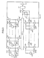
- Fig. 1 shows the diagram of a linear self-adjusting corrector of a known type which comprises, on the one hand, a recursive transversal filter 1 and, on the other hand, a calculation circuit 2, 3 and 4.
- the filter 1 is similar to that shown in FIG. A.2. from page 489 of the already cited work.
- the signal to be corrected x (t) is applied to the input of a first chain of r cells connected in series and each providing a delay equal to T where T is the inverse of the bit frequency.
- the outputs of the r cells are connected to the first inputs of r multipliers whose multiplication coefficients are respectively al to ar.
- the outputs of the r multipliers are connected to corresponding inputs of a summator S.
- the output of the summator S which delivers the corrected signal y (t), is also connected to a chain of m cells connected in series and each providing a delay T.
- the outputs of the m cells are connected to the inputs of m multipliers whose multiplier coefficients are respectively bl to bm.
- the outputs of the m multipliers are connected to corresponding inputs of the summator S.
- the calculation circuit 2 delivers the coefficients al to ar and bl to bm which are applied, in filter 1, to the corresponding inputs of the multipliers.
- the input of the calculation circuit 2 is connected to the output of a comparator 3, one input of which is connected directly to the output of the filter 1 and the other input of which is connected to the output of a threshold detector 4, the l the signal input is also connected to the output of the filter 1.
- the threshold detector 4 has a control input 5 to which a reference voltage defining the thresholds is applied.
- the filter 1 is a direct and non-recursive filter, which amounts to canceling the coefficients bl to bm.
- the threshold detector 4 is added in the recursive part. If a reference signal is directly applied to the second input of comparator 3, the filter then being only adaptive instead of being self-adaptive.
- the reference voltage applied to the control input 5 of the threshold detector 4 is generally equal to the average value of the amplitude of the output signal of the filter 1.
- the output signal of the threshold detector 4 therefore corresponds to a value estimated (t) of the output signal y (t).
- the correcting criterion is that of the mean square error: where a k is the transmitted signal, which is replaced by an estimated value in the case of a self-adaptive filter. In an autoadaptive filter, one seeks the coefficients composing the vector H which minimize this expression.
- An object of the invention is to provide a correction device comprising an analog linear filter whose coefficients can be determined by applying digital calculation techniques.
- a correction device comprising an analog transverse filter and a calculation circuit delivering the coefficients al to ar and, optionally, bl to bm of the analog transversal filter, the input of the calculation circuit being connected to the input of the analog transversal filter and the calculation circuit comprising an analog / digital converter whose output is connected to a self-adapting digital transversal filter, some, at least, of the coefficients of the multipliers of the digital transversal filter being applied to the multipliers of the analog cross filter.
- the analog transversal filter is of the same type as the digital transversal filter.
- the optimization criterion is that of the mean square error and the convergence algorithm is that of the gradient, the iterative correction being carried out at each step on the set of coefficients of the filter.
- the optimization criterion is that of the mean square error and the convergence algorithm is that of the gradient, the iterative correction being cyclically performed on each of the coefficients.
- the video signal carrying the data is applied to the input E which is connected in parallel, on the one hand, to a transverse filter 6 and, on the other hand, to a calculation circuit 7.
- the filter 6 operates directly on the analog signal applied to the input El and delivers a corrected analog signal which is applied to a DIDON 8 demodulator which is preferably of the type of receiver described in patent FR-2 313 825.
- the calculation circuit 7 comprises a clamping circuit 9, the output of which is connected in parallel to a mean value calculation circuit 10, a synchronization circuit 11 and to an analog-digital converter 12, the output of which is connected to a memory 13
- the calculation circuit 7 also comprises a microprocessor 14.
- the software of the microprocessor 14 is provided so that the calculation circuit 7 functions, for example, as a recursive self-adapting transverse filter with decision in the loop.
- the sampling frequency is equal to the bit frequency, the sampling instant being centered in each elementary time.
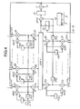
- the diagram in FIG. 3 symbolizes the filter constituted by the calculation circuit 7.
- the samples X (t), coming from the analog-digital converter 12, are applied to the input of a chain of 1 registers RD1 to RD1.
- the outputs of registers RD1 to RD1 are respectively connected to the first inputs of 1 digital multipliers Al to Al whose outputs are connected to the first 1 inputs of a digital summator SOM1.
- the registers RD1 to RD1 can operate in shift register with a clock of period T.
- the output of the summator SOM1 is connected, on the one hand, to the input of a threshold detector DS and, on the other hand, to the input - of a summator SOM2 whose input + is connected to the DS detector output.
- the output of the detector DS is connected to the input of a chain of p shift registers RR1 to RRp.
- the outputs of the registers RR1 to RRp are respectively connected to the first inputs of p multipliers B1 to B1 whose outputs are connected to p inputs of the summator SOM1.
- the registers RR1 to RR1 can form a shift register with a clock of period T.
- the input for controlling the threshold level in the detector DS is connected to the output of the average value calculation circuit 10.
- the elements of the diagram in FIG. 3 which have just been described constitute a part of a recursive transverse digital filter with decision in the loop.
- the other part of the filter must include a circuit for calculating the coefficients of the multipliers Al to Al and Bl to Bp. We will now describe this calculation circuit.
- the output of the summator SOM2 is connected to an estimation circuit CE, the output of which is connected to a multiplier C at the second input from which the value of a coefficient u is applied.
- the output of the multiplier C is connected to the first inputs of a first series of multipliers Dl to Dl and of a second series of multipliers El to Ep.
- the second inputs of the multipliers Dl to Dl are respectively connected to the outputs of the registers RD1 to RD1 .
- the second inputs of multipliers El to Ep are respectively connected to the outputs of registers RR1 to RRp.
- the outputs of the multipliers Dl to Dl are respectively connected to the inputs - of summers ADD1 to ADDl whose outputs are respectively connected, on the one hand, to the second inputs of the multipliers A1 to Al and, on the other hand, to the memory inputs MD1 to MD1.
- the outputs of memories MD1 to MD1 are respectively connected to the inputs + of summers ADD1 to ADD1.
- the outputs of the multipliers El to Ep are respectively connected to the inputs - of summers ADR1 to ADRp whose outputs are respectively connected, on the one hand, to the second inputs of the multipliers B1 to Bp and, on the other hand, to the memory inputs MR1 at MRp.
- the outputs of memories MR1 to MRp are respectively connected to the inputs + of summers ADR1 to ADRp.
- the memories MD1 to MD1 present at their outputs, at the sampling instant k, the values H1 k to Hl k which have been written there at the sampling instant (k-1). Under the same conditions, the memories MR1 to MRp deliver the values Jl k to J p k .
- the output signal from the summator SOM2 corresponds to the difference e between the estimated signal a k delivered by the detector DS and the output signal y k from the summator SOM1.
- the indices k indicate the rank of the digital samples considered.
- the signal e is therefore an error signal which is processed in the estimation circuit CE.
- the quadratic mean error is used as the optimization criterion for the corrector. If F (H) represents the mean square error, we have: where the vector H is the vector corresponding to the coefficients Hl to Hl.
- the algorithm chosen to minimize the criterion F (H) is, in an exemplary embodiment according to the invention, the gradient algorithm which is defined below.
- the first member of the equal The above is a positive quantity.
- the second member being the scalar product of two vectors, it is necessary that is of opposite direction to ⁇ .F ( H k ) and that it be parallel to it to increase this scalar product, which implies: Is:
- the convergence step of the algorithm is a constant value u which is chosen to be close to the value ⁇ defined above.
- the circuit CE is designed to deliver the signal sg (e k ). We therefore have, on the first inputs of the multipliers Dl to Dl, the signal u.sg (e k ) and, like the second inputs of the summers ADD1 to ADDl form the components of the vector H k , we have at the output of the same summers the components of the vector H k + 1 .
- the different operations - additions, multiplications, delays - which are carried out by the corresponding elements - summers, multipliers, registers - shown in FIG. 3 can also be carried out using appropriate software of the microprocessor 14 of FIG. 2. Indeed, all the samples X k , Y k , H1 k to Hl k , il k to Jp are available in memory 13, which also contains the value of u and possibly of u '. Finally, for the operation of the threshold decision circuit DS, the mean value calculation circuit 9 periodically supplies this value which is also stored in memory 13.
- the calculation circuit 7 of FIG. 2 also includes a buffer register 15 in which the vector coefficients are stored H k , that is to say the output coefficients of the memories MD1 to MD1.
- the outputs of the buffer register are respectively connected to control inputs of the analog linear filter 6, these control inputs delivering the coefficients of the multipliers of the filter 6.
- the filter 6 can be constituted by a series of delay cells, each cell providing a delay T.
- an analog multiplier circuit is inserted, an input of which is connected at the end of the length of upstream cable and the outlet at the input of the downstream cable length.
- the other input of the multiplier is connected to the output of a digital-analog converter whose digital input is connected to the corresponding output of the buffer register 15.
- the content of the buffer register 15 is refreshed only periodically, for example every ten seconds. After each new loading of the register 15, the coefficients already calculated are kept in the memory 13. On the other hand, the samples present in this memory are replaced by the new incoming samples.
- one of the coefficients Hl to Hl takes the value 1 while the other coefficients are zero, as well as the coefficients J1 to Jp.
- the rank of the coefficient initially set to 1 defines what is known as the central coefficient. The choice of the central coefficient makes it possible to define the maximum temporal deviation of the echoes that the filter can correct.
Abstract
Description
La présente invention concerne un dispositif de correction d'échos en transmission numérique, c'est-à-dire de correction d'interférence entre symboles, la correction étant effectuée sur le signal analogique démodulé reçu. Plus particulièrement, l'invention concerne un dispositif de correction d'échos intervenant dans un système de télédiffusion de données, tel que celui qui est décrit dans le brevet FR-2 313 825 et qui est mis en oeuvre sous le nom de "Réseau DIDON" par l'Etablissement public de diffusion dit "Télédiffusion de France".The present invention relates to an echo correction device in digital transmission, that is to say interference correction between symbols, the correction being carried out on the received demodulated analog signal. More particularly, the invention relates to an echo correction device intervening in a data broadcasting system, such as that which is described in patent FR-2 313 825 and which is implemented under the name of "DIDON network "by the public broadcasting establishment known as" Télédiffusion de France ".
Dans le réseau DIDON, les données binaires sont transmises en modulation d'amplitude en code NRZ par paquets sur des lignes d'image de télévision diffusées notamment par voies hertzienne et la fréquence bit est de 6,2 MHz. Le canal de télédiffusion apporte un certain nombre de perturbations au signal vidéo, tels que des évanouissements sélectifs, du bruit et des échos résultant de réflexions proches du lieu de réception. La réponse impulsionnelle se trouve donc déformée et, compte tenu de la fréquence bit élevée qui est utilisée, il en résulte un phénomène de chevauchement des impulsions, c'est-à-dire un phénomène d'interférence entre symboles. Comme les phénomènes d'échos accroissent la sensibilité du signal au bruit et aux parasites, il est important de prévoir, dans les récepteurs de données du réseau DIDON, un correcteur d'échos.In the DIDON network, binary data is transmitted in amplitude modulation in NRZ code in packets on television image lines broadcast in particular by radio channels and the bit frequency is 6.2 MHz. The broadcasting channel brings a number of disturbances to the video signal, such as selective fading, noise and echoes resulting from reflections close to the reception site. The impulse response is therefore distorted and, given the high bit frequency which is used, this results in a phenomenon of overlapping of the pulses, that is to say a phenomenon of interference between symbols. Like the phenomena of echoes increase the sensitivity of the signal to noise and noise, it is important to provide an echo corrector in the DIDON network data receivers.
Dans l'ouvrage "TELEINFORMATIQUE transport et traitement de l'information dans les réseaux et systèmes téléinformatiques" par C. Macchi et J-F. Guilbert (Ed. DUNOD 1979), le phénomène des interférences entre symboles est traité au § 3.1.4. Pour réduire ces interférences, on prévoit un récepteur linéaire à filtre numérique, éventuellement adaptatif, comme cela est indiqué au § 3.3.3.F. Un filtre numérique linéaire est décrit au § A.2.2 de ce même ouvrage.In the book "TELEINFORMATIQUE transport and processing of information in networks and teleinformatic systems" by C. Macchi and J-F. Guilbert (Ed. DUNOD 1979), the phenomenon of interference between symbols is dealt with in § 3.1.4. To reduce this interference, a linear receiver with digital filter, possibly adaptive, is provided, as indicated in § 3.3.3.F. A linear digital filter is described in § A.2.2 of this same book.
La Fig. 1 montre le schéma d'un correcteur autoadaptatif linéaire d'un type connu qui comprend, d'une part, un filtre transversal récursif 1 et, d'autre part, un circuit de calcul 2, 3 et 4. Le filtre 1 est semblable à celui qui est montré à la Fig. A.2. de la page 489 de l'ouvrage déjà cité. Dans le filtre 1, le signal à corriger x(t) est appliqué à l'entrée d'une première chaîne de r cellules montées en série et apportant chacune un retard égal à T où T est l'inverse de la fréquence bit. Les sorties des r cellules sont reliées aux premières entrées de r multiplicateurs dont les coefficients de multiplication sont respectivement al à ar. Les sorties des r multiplicateurs sont reliées à des entrées correspondantes d'un sommateur S. La sortie du sommateur S, qui délivre le signal corrigé y(t), est également reliée à une chaîne de m cellules montées en série et apportant chacune un retard T. Les sorties des m cellules sont reliées aux entrées de m multiplicateurs dont les coefficients multiplicateurs sont respectivement bl à bm. Les sorties des m multiplicateurs sont reliées à des entrées correspondantes du sommateur S. Le circuit de calcul 2 délivre les coefficients al à ar et bl à bm qui sont appliqués, dans le filtre 1, aux entrées correspondantes des multiplicateurs. L'entrée du circuit de calcul 2 est reliée à la sortie d'un comparateur 3 dont une entrée est reliée directement à la sortie du filtre 1 et dont l'autre entrée est reliée à la sortie d'un détecteur à seuils 4 dont l'entrée de signal est également reliée à la sortie du filtre 1. Le détecteur à seuils 4 a une entrée de commande 5 à laquelle est appliquée une tension de référence définissant les seuils.Fig. 1 shows the diagram of a linear self-adjusting corrector of a known type which comprises, on the one hand, a recursive
Il existe des variantes du correcteur de la Fig. 1. Dans une première variante, le filtre 1 est un filtre direct et non récursif, ce qui revient à annuler les coefficients bl à bm. Dans une seconde variante, le détecteur à seuil 4 est ajouté dans la partie récursive. Si un signal de référence est directement appliqué à la seconde entrée du comparateur 3, le filtre étant alors uniquement adaptatif au lieu d'être autoadaptatif.There are variants of the corrector in FIG. 1. In a first variant, the
La tension de référence appliquée à l'entrée de commande 5 du détecteur à seuil 4 est généralement égale à la valeur moyenne de l'amplitude du signal de sortie du filtre 1. Le signal de sortie du détecteur à seuil 4 correspond donc à une valeur estimée (t) du signal de sortie y(t). Le comparateur 3 délivre donc l'erreur e(t) = y(t) - y(t). Dans le circuit de calcul 2, on utilise comme critère d'optimisation du correcteur celui de l'erreur quadratique moyenne:![]()
![]()
Un objet de l'invention consiste à prévoir un dispositif de correction comprenant un filtre linéaire analogique dont les coefficients peuvent être déterminés en appliquant des techniques de calcul numérique.An object of the invention is to provide a correction device comprising an analog linear filter whose coefficients can be determined by applying digital calculation techniques.
Suivant une caractéristique de l'invention, il est prévu un dispositif de correction comprenant un filtre transversal analogique et un circuit de calcul délivrant les coefficients al à ar et, éventuellement, bl à bm du filtre transversal analogique, l'entrée du circuit de calcul étant reliée à l'entrée du filtre transversal analogique et le circuit de calcul comprenant un convertisseur analogique/numérique dont la sortie est reliée à un filtre transversal numérique autoadaptatif, certains, au moins, des coefficients des multiplicateurs du filtre transversal numérique étant appliqués aux multiplicateurs du filtre transversal analogique.According to a characteristic of the invention, there is provided a correction device comprising an analog transverse filter and a calculation circuit delivering the coefficients al to ar and, optionally, bl to bm of the analog transversal filter, the input of the calculation circuit being connected to the input of the analog transversal filter and the calculation circuit comprising an analog / digital converter whose output is connected to a self-adapting digital transversal filter, some, at least, of the coefficients of the multipliers of the digital transversal filter being applied to the multipliers of the analog cross filter.
Suivant une autre caractéristique, le filtre transversal analogique est du même type que le filtre transversal numérique.According to another characteristic, the analog transversal filter is of the same type as the digital transversal filter.
Suivant une autre caractéristique, dans le circuit de calcul, le critère d'optimisation est celui de l'erreur quadratique moyenne et l'algorithme de convergence est celui du gradient, la correction itérative étant effectuée à chaque pas sur l'ensemble des coefficients du filtre.According to another characteristic, in the calculation circuit, the optimization criterion is that of the mean square error and the convergence algorithm is that of the gradient, the iterative correction being carried out at each step on the set of coefficients of the filter.
Suivant une autre caractéristique, le critère d'optimisation est celui de l'erreur quadratique moyenne et l'algorithme de convergence est celui du gradient, la correction itérative étant cycliquement effectuée sur chacun des coefficients.According to another characteristic, the optimization criterion is that of the mean square error and the convergence algorithm is that of the gradient, the iterative correction being cyclically performed on each of the coefficients.
Les caractéristiques de l'invention mentionnées ci-dessus, ainsi que d'autres, apparaîtront plus clairement à la lecture de la description suivante d'un exemple de réalisation, ladite description étant faite en relation avec les dessins joints, parmi lesquels:
- la Fig. 1 est le schéma d'un dispositif de correction faisant partie de l'état de la technique,
- la Fig. 2 est un bloc-diagramme d'un dispositif de correction suivant l'invention,
- la Fig. 3 est un bloc-diagramme schématique d'un circuit de calcul formé de circuits discrets fonctionnant comme le circuit de calcul de la Fig. 2, et
- la Fig. 4 est un bloc-diagramme d'une variante du circuit de calcul de la Fig. 3.
- Fig. 1 is the diagram of a correction device forming part of the state of the art,
- Fig. 2 is a block diagram of a correction device according to the invention,
- Fig. 3 is a schematic block diagram of a calculation circuit formed by discrete circuits operating like the calculation circuit of FIG. 2, and
- Fig. 4 is a block diagram of a variant of the calculation circuit of FIG. 3.
Dans le circuit de correction de la Fig. 2, le signal' vidéo portant les données est appliqué à l'entrée E qui est reliée en parallèle, d'une part, à un filtre transversal 6 et, d'autre part, à un circuit de calcul 7. Le filtre 6 fonctionne directement sur le signal analogique appliqué à l'entrée El et délivre un signal analogique corrigé lequel est appliqué à un démodulateur DIDON 8 qui est, de préférence, du type du récepteur décrit dans le brevet FR-2 313 825.In the correction circuit of FIG. 2, the video signal carrying the data is applied to the input E which is connected in parallel, on the one hand, to a transverse filter 6 and, on the other hand, to a calculation circuit 7. The filter 6 operates directly on the analog signal applied to the input El and delivers a corrected analog signal which is applied to a DIDON 8 demodulator which is preferably of the type of receiver described in patent FR-2 313 825.
Le circuit de calcul 7 comprend un circuit de clampage 9 dont la sortie est reliée en parallèle à un circuit de calcul de valeur moyenne 10, un circuit de synchronisation 11 et à un convertisseur analogique-numérique 12 dont la sortie est reliée à une mémoire 13. Le circuit de calcul 7 comprend encore un microprocesseur 14. Le logiciel du microprocesseur 14 est prévu de manière que le circuit de calcul 7 fonctionne, par exemple, comme un filtre transversal récursif autoadaptatif avec décision dans la boucle.The calculation circuit 7 comprises a clamping circuit 9, the output of which is connected in parallel to a mean
Dans le convertisseur analogique-numérique 12, la fréquence d'échantillonnage est égale à la fréquence bit, l'instant d'échantillonnage étant centré dans chaque temps élémentaire.In the analog-
Le schéma de la Fig. 3 symbolise le filtre constitué par le circuit de calcul 7. Les échantillons X(t), provenant du convertisseur analogique-numérique 12, sont appliqués à l'entrée d'une chaîne de 1 registres RD1 à RD1. Les sorties des registres RD1 à RD1 sont respectivement reliées aux premières entrées de 1 multiplicateurs numériques Al à Al dont les sorties sont reliées aux 1 premières entrées d'un sommateur numérique SOM1. Les registres RD1 à RD1 peuvent fonctionner en registre à décalage avec une horloge de période T.The diagram in FIG. 3 symbolizes the filter constituted by the calculation circuit 7. The samples X (t), coming from the analog-
La sortie du sommateur SOM1 est reliée, d'une part, à l'entrée d'un détecteur à seuil DS et, d'autre part, à l'entrée - d'un sommateur SOM2 dont l'entrée + est reliée à la sortie du détecteur DS.The output of the summator SOM1 is connected, on the one hand, to the input of a threshold detector DS and, on the other hand, to the input - of a summator SOM2 whose input + is connected to the DS detector output.
La sortie du détecteur DS est reliée à l'entrée d'une chaîne de p registres à décalages RR1 à RRp. Les sorties des registres RR1 à RRp sont respectivement reliées aux premières entrées de p multiplicateurs B1 à Bl dont les sorties sont reliées à p entrées du sommateur SOM1. Les registres RR1 à RR1 peuvent former un registre à décalage avec une horloge de période T. L'entrée de commande du niveau du seuil dans le détecteur DS est reliée à la sortie du circuit de calcul de valeur moyenne 10.The output of the detector DS is connected to the input of a chain of p shift registers RR1 to RRp. The outputs of the registers RR1 to RRp are respectively connected to the first inputs of p multipliers B1 to B1 whose outputs are connected to p inputs of the summator SOM1. The registers RR1 to RR1 can form a shift register with a clock of period T. The input for controlling the threshold level in the detector DS is connected to the output of the average
Les éléments du schéma de la Fig. 3 qui viennent d'être décrits constituent une partie d'un filtre numérique transversal récursif avec décision dans la boucle. L'autre partie du filtre doit comprendre un circuit de calcul des coefficients des multiplicateurs Al à Al et Bl à Bp. On va maintenant décrire ce circuit de calcul.The elements of the diagram in FIG. 3 which have just been described constitute a part of a recursive transverse digital filter with decision in the loop. The other part of the filter must include a circuit for calculating the coefficients of the multipliers Al to Al and Bl to Bp. We will now describe this calculation circuit.
La sortie du sommateur SOM2 est reliée à un circuit d'estimation CE dont la sortie est reliée à un multiplicateur C à la seconde entrée duquel est appliquée la valeur d'un coefficient u.The output of the summator SOM2 is connected to an estimation circuit CE, the output of which is connected to a multiplier C at the second input from which the value of a coefficient u is applied.
La sortie du multiplicateur C est reliée aux premières entrées d'une première série de multiplicateurs Dl à Dl et d'une seconde série de multiplicateurs El à Ep. Les secondes entrées des multiplicateurs Dl à Dl sont respectivement reliées aux sorties des registres RD1 à RD1. Les secondes entrées des multiplicateurs El à Ep sont respectivement reliées aux sorties des registres RR1 à RRp.The output of the multiplier C is connected to the first inputs of a first series of multipliers Dl to Dl and of a second series of multipliers El to Ep. The second inputs of the multipliers Dl to Dl are respectively connected to the outputs of the registers RD1 to RD1 . The second inputs of multipliers El to Ep are respectively connected to the outputs of registers RR1 to RRp.
Les sorties des multiplicateurs Dl à Dl sont respectivement reliées aux entrées - de sommateurs ADD1 à ADDl dont les sorties sont respectivement reliées, d'une part, aux secondes entrées des multiplicateurs A1 à Al et, d'autre part, aux entrées de mémoires MD1 à MD1. Les sorties des mémoires MD1 à MD1 sont respectivement reliées aux entrées + des sommateurs ADD1 à ADD1.The outputs of the multipliers Dl to Dl are respectively connected to the inputs - of summers ADD1 to ADDl whose outputs are respectively connected, on the one hand, to the second inputs of the multipliers A1 to Al and, on the other hand, to the memory inputs MD1 to MD1. The outputs of memories MD1 to MD1 are respectively connected to the inputs + of summers ADD1 to ADD1.
Les sorties des multiplicateurs El à Ep sont respectivement reliées aux entrées - de sommateurs ADR1 à ADRp dont les sorties sont respectivement reliées, d'une part, aux secondes entrées des multiplicateurs Bl à Bp et, d'autre part, aux entrées de mémoires MR1 à MRp. Les sorties des mémoires MR1 à MRp sont respectivement reliées aux entrées + des sommateurs ADR1 à ADRp.The outputs of the multipliers El to Ep are respectively connected to the inputs - of summers ADR1 to ADRp whose outputs are respectively connected, on the one hand, to the second inputs of the multipliers B1 to Bp and, on the other hand, to the memory inputs MR1 at MRp. The outputs of memories MR1 to MRp are respectively connected to the inputs + of summers ADR1 to ADRp.
Les mémoires MD1 à MD1 présentent à leurs sorties, à l'instant d'échantillonnage k, les valeurs H1k à Hlk qui y ont été écrites à l'instant d'échantillonnage (k-1). Dans les mêmes conditions, les mémoires MR1 à MRp délivrent les valeurs Jl k à Jpk.The memories MD1 to MD1 present at their outputs, at the sampling instant k, the values H1 k to Hl k which have been written there at the sampling instant (k-1). Under the same conditions, the memories MR1 to MRp deliver the values Jl k to J p k .
Dans la pratique, le signal de sortie du sommateur SOM2 correspond à l'écart e entre le signal estimé ak délivré par le détecteur DS et le signal de sortie yk du sommateur SOM1. Les indices k indiquent le rang des échantillons numériques considérés.In practice, the output signal from the summator SOM2 corresponds to the difference e between the estimated signal a k delivered by the detector DS and the output signal y k from the summator SOM1. The indices k indicate the rank of the digital samples considered.
Le signal e est donc un signal d'erreur qui est traité dans le circuit d'estimation CE.The signal e is therefore an error signal which is processed in the estimation circuit CE.
Comme on l'a mentionné plus haut, on utilise, comme critère d'optimisation du correcteur, celui de l'erreur quadratique moyenne. Si F(H) représente l'erreur quadratique moyenne, on a:![]()
![]()
L'algorithme choisi pour minimiser le critère F(H) est, dans un exemple de réalisation suivant l'invention, l'algorithme du gradient qui est défini ci-dessous.The algorithm chosen to minimize the criterion F (H) is, in an exemplary embodiment according to the invention, the gradient algorithm which is defined below.
On désire obtenir que la différence (F(Hk) - F(Hk+1)) soit minimale. Si l'on pose:![]()
![]()
![]()
![]()
Dans le sens d'une minimalisation, le premier membre de l'égalité ci-dessus est une grandeur positive. Le second membre étant le produit scalaire de deux vecteurs, il faut que soit de sens opposé à Δ .F(![]()
![]()
![]()
![]()
D'autre part: avec:![]()
![]()
![]()
![]()
On a donc:
Le pas de convergence de l'algorithme est une valeur constante u que l'on choisit voisine de la valeur µ définie ci-dessus.The convergence step of the algorithm is a constant value u which is chosen to be close to the value µ defined above.
Dans la pratique, on peut négliger la valeur de ek, et ne conserver que son signe sg(ek), la valeur de u est ajustée en conséquence.In practice, we can neglect the value of e k , and keep only its sign sg (e k ), the value of u is adjusted accordingly.
Dans l'exemple de réalisation de la Fig. 3, le circuit CE est prévu pour délivrer le signal sg(ek). On a donc, sur les premières entrées des multiplicateurs Dl à Dl, le signal u.sg(ek) et, comme les secondes entrées des sommateurs ADD1 à ADDl forment les composantes du vecteur
Dans la description qui précède, on n'a considéré que le vecteur
Dans la pratique, les différentes opérations - additions, multiplications, retards - qui sont effectuées par les éléments correspondants - sommateurs, multiplicateurs, registres - montrés à la Fig. 3 peuvent également être effectuées à l'aide d'un logiciel approprié du microprocesseur 14 de la Fig. 2. En effet, tous les échantillons Xk, Y k, H1 k à Hlk, ilk à Jp sont disponibles dans la mémoire 13, qui contient également la valeur de u et éventuellement de u'. Enfin, pour le fonctionnement du circuit de décision à seuil DS, le circuit de calcul de la valeur moyenne 9 fournit périodiquement cette valeur qui est aussi mémorisée dans la mémoire 13.In practice, the different operations - additions, multiplications, delays - which are carried out by the corresponding elements - summers, multipliers, registers - shown in FIG. 3 can also be carried out using appropriate software of the
Le circuit de calcul 7 de la Fig. 2 comprend encore un registre tampon 15 dans lequel sont mémorisés les coefficients du vecteur
Le filtre 6 peut être constitué par une série de cellules à retard, chaque cellule apportant un retard T. Au point de jonction entre deux longueurs de câble, est inséré un circuit multiplicateur analogique, dont une entrée est reliée à la fin de la longueur de câble amont et la sortie à l'entrée de la longueur de câble aval. L'autre entrée du multiplieur est reliée à la sortie d'un convertisseur numérique-analogique dont l'entrée numérique est reliée à la sortie correspondante du registre tampon 15.The filter 6 can be constituted by a series of delay cells, each cell providing a delay T. At the junction between two lengths of cable, an analog multiplier circuit is inserted, an input of which is connected at the end of the length of upstream cable and the outlet at the input of the downstream cable length. The other input of the multiplier is connected to the output of a digital-analog converter whose digital input is connected to the corresponding output of the
En pratique, le contenu du registre tampon 15 n'est rafraîchi que périodiquement, par exemple toutes les dix secondes. Après chaque nouveau chargement du registre 15, les coefficients déjà calculés sont conservés dans la mémoire 13. Par contre, les échantillons présents dans cette mémoire sont remplacés par les nouveaux échantillons entrants.In practice, the content of the
Dans le bloc-diagramme de la Fig. 4, on retrouve tous les éléments de celui de la Fig. 3. Il comporte, en supplément, un compteur cyclique CC à 1+p étages dont les 1+p sorties sont respectivement reliées aux premières entrées de portes ET ETD1 à ETD1 et ETR1 à ETRp dont les secondes entrées sont reliées à la sortie du multiplicateur C et les sorties sont' respectivement reliées aux premières entrées des multiplicateurs Dl à Dl et El à Ep.In the block diagram of FIG. 4, we find all the elements of that of FIG. 3. It includes, in addition, a cyclic counter CC with 1 + p stages whose 1 + p outputs are respectively connected to the first door inputs ET ETD1 to ETD1 and ETR1 to ETRp whose second inputs are connected to the output of the multiplier C and the outputs are respectively connected to the first inputs of the multipliers Dl to Dl and El to Ep.
Dans le circuit de la Fig. 4, on utilise l'algorithme:![]()
![]()
A l'instant initial, du fonctionnement du filtre de l'invention, l'un des coefficients Hl à Hl prend la valeur 1 tandis que les autres coefficients sont nuls, ainsi que les coefficients J1 à Jp. Le rang du coefficient mis initialement à 1 définit ce qu'il est convenu d'appeler le coefficient central. Le choix du coefficient central permet de définir l'écart maximal temporel des échos que le filtre peut corriger.At the initial instant, during the operation of the filter of the invention, one of the coefficients Hl to Hl takes the
L'expérience a montré que l'on obtenait, dans le cas de la télédiffusion de données DIDON, de bons résultats en utilisant un filtre transversal numérique, non récursif, comprenant dix cellules de retard, dans lequel le coefficient central est affecté à la quatrième cellule.Experience has shown that in the case of DIDON data broadcasting, good results are obtained by using a non-recursive digital transversal filter comprising ten delay cells, in which the central coefficient is assigned to the fourth cell.
Claims (7)
Priority Applications (1)
| Application Number | Priority Date | Filing Date | Title |
|---|---|---|---|
| AT84460007T ATE34495T1 (en) | 1983-10-28 | 1984-10-09 | DEVICE FOR ECHO CORRECTION, PARTICULARLY FOR A TELEVISION DATA TRANSMISSION SYSTEM. |
Applications Claiming Priority (2)
| Application Number | Priority Date | Filing Date | Title |
|---|---|---|---|
| FR8317438 | 1983-10-28 | ||
| FR8317438A FR2556530B1 (en) | 1983-10-28 | 1983-10-28 | ECHO CORRECTION DEVICE, ESPECIALLY FOR A DATA BROADCASTING SYSTEM |
Publications (2)
| Publication Number | Publication Date |
|---|---|
| EP0140809A1 true EP0140809A1 (en) | 1985-05-08 |
| EP0140809B1 EP0140809B1 (en) | 1988-05-18 |
Family
ID=9293722
Family Applications (1)
| Application Number | Title | Priority Date | Filing Date |
|---|---|---|---|
| EP84460007A Expired EP0140809B1 (en) | 1983-10-28 | 1984-10-09 | Echo correction apparatus, particularly for a television data transmission system |
Country Status (12)
| Country | Link |
|---|---|
| US (1) | US4696015A (en) |
| EP (1) | EP0140809B1 (en) |
| JP (1) | JPS60111537A (en) |
| AT (1) | ATE34495T1 (en) |
| AU (1) | AU566962B2 (en) |
| BR (1) | BR8405550A (en) |
| CA (1) | CA1217856A (en) |
| DE (1) | DE3471414D1 (en) |
| ES (1) | ES8507300A1 (en) |
| FR (1) | FR2556530B1 (en) |
| MX (1) | MX155974A (en) |
| PT (1) | PT79396B (en) |
Cited By (1)
| Publication number | Priority date | Publication date | Assignee | Title |
|---|---|---|---|---|
| EP0409756A1 (en) * | 1989-07-18 | 1991-01-23 | France Telecom | Data reception device with delayed equalizing and retroactive clock recovery |
Families Citing this family (13)
| Publication number | Priority date | Publication date | Assignee | Title |
|---|---|---|---|---|
| US4811261A (en) * | 1985-03-04 | 1989-03-07 | Oki Electric Industry Co., Ltd. | Adaptive digital filter for determining a transfer equation of an unknown system |
| EP0231854B1 (en) * | 1986-01-30 | 1991-04-03 | Siemens Aktiengesellschaft | Echo compensator |
| US5058047A (en) * | 1989-05-30 | 1991-10-15 | Advanced Micro Devices, Inc. | System and method for providing digital filter coefficients |
| US5535150A (en) * | 1993-04-20 | 1996-07-09 | Massachusetts Institute Of Technology | Single chip adaptive filter utilizing updatable weighting techniques |
| US6542611B1 (en) * | 1998-07-31 | 2003-04-01 | Circuit Research Labs, Inc. | Multi-state echo suppressor |
| DE19925046A1 (en) * | 1999-06-01 | 2001-05-03 | Alcatel Sa | Method and device for suppressing noise and echoes |
| US6480532B1 (en) * | 1999-07-13 | 2002-11-12 | Stmicroelectronics, Inc. | Echo cancellation for an ADSL modem |
| FR2801753B1 (en) * | 1999-11-25 | 2002-05-03 | Groupe Ecoles Telecomm | IMPROVEMENTS ON ADAPTIVE EQUALIZATION DEVICES FOR RECOVERIES OF DIGITAL COMMUNICATION SYSTEMS |
| US8295475B2 (en) * | 2006-01-13 | 2012-10-23 | Microsoft Corporation | Selective glitch detection, clock drift compensation, and anti-clipping in audio echo cancellation |
| US7831035B2 (en) * | 2006-04-28 | 2010-11-09 | Microsoft Corporation | Integration of a microphone array with acoustic echo cancellation and center clipping |
| US7773743B2 (en) * | 2006-04-28 | 2010-08-10 | Microsoft Corporation | Integration of a microphone array with acoustic echo cancellation and residual echo suppression |
| US8380253B2 (en) | 2008-02-15 | 2013-02-19 | Microsoft Corporation | Voice switching for voice communication on computers |
| US8369251B2 (en) * | 2008-06-20 | 2013-02-05 | Microsoft Corporation | Timestamp quality assessment for assuring acoustic echo canceller operability |
Citations (2)
| Publication number | Priority date | Publication date | Assignee | Title |
|---|---|---|---|---|
| US3787645A (en) * | 1971-05-19 | 1974-01-22 | Nippon Electric Co | Echo canceller having two echo path models |
| EP0052362A1 (en) * | 1980-11-17 | 1982-05-26 | Nec Corporation | Fast start-up system for transversal equalizers |
Family Cites Families (7)
| Publication number | Priority date | Publication date | Assignee | Title |
|---|---|---|---|---|
| NL171215C (en) * | 1973-03-09 | 1983-02-16 | Trt Telecom Radio Electr | AUTOMATIC EQUALIZATION DEVICE FOR A DATA TRANSMISSION CHANNEL. |
| FR2370396A1 (en) * | 1976-11-09 | 1978-06-02 | Cit Alcatel | SELF-ADAPTIVE EQUALIZATION KIT |
| FR2410917A1 (en) * | 1977-11-30 | 1979-06-29 | Cit Alcatel | SELF-ADAPTIVE EQUALIZER |
| US4321686A (en) * | 1980-01-24 | 1982-03-23 | Communications Satellite Corporation | Correction processor of self-adaptive filters |
| FR2479617A1 (en) * | 1980-03-26 | 1981-10-02 | Trt Telecom Radio Electr | ECHO CANCELLATOR FOR ECHO SIGNAL WITH VARIABLE PHASE |
| JPS56169919A (en) * | 1980-06-03 | 1981-12-26 | Toshiba Corp | Automatic equalizer |
| FR2541837A1 (en) * | 1983-02-25 | 1984-08-31 | Trt Telecom Radio Electr | METHOD FOR REDUCING THE CONVERGENCE TIME OF AN ECHO CANCER AND DEVICE FOR CARRYING OUT SAID METHOD |
-
1983
- 1983-10-28 FR FR8317438A patent/FR2556530B1/en not_active Expired
-
1984
- 1984-10-09 EP EP84460007A patent/EP0140809B1/en not_active Expired
- 1984-10-09 DE DE8484460007T patent/DE3471414D1/en not_active Expired
- 1984-10-09 AT AT84460007T patent/ATE34495T1/en active
- 1984-10-19 US US06/662,961 patent/US4696015A/en not_active Expired - Fee Related
- 1984-10-19 CA CA000465957A patent/CA1217856A/en not_active Expired
- 1984-10-24 PT PT79396A patent/PT79396B/en unknown
- 1984-10-26 MX MX203190A patent/MX155974A/en unknown
- 1984-10-26 BR BR8405550A patent/BR8405550A/en unknown
- 1984-10-26 ES ES537153A patent/ES8507300A1/en not_active Expired
- 1984-10-26 AU AU34756/84A patent/AU566962B2/en not_active Ceased
- 1984-10-29 JP JP59225996A patent/JPS60111537A/en active Pending
Patent Citations (2)
| Publication number | Priority date | Publication date | Assignee | Title |
|---|---|---|---|---|
| US3787645A (en) * | 1971-05-19 | 1974-01-22 | Nippon Electric Co | Echo canceller having two echo path models |
| EP0052362A1 (en) * | 1980-11-17 | 1982-05-26 | Nec Corporation | Fast start-up system for transversal equalizers |
Non-Patent Citations (3)
| Title |
|---|
| IEEE TRANSACTIONS ON CONSUMER ELECTRONICS, vol. CE-27, no. 3, août 1981, pages 512-529, New York, US; J.O. VOORMAN et al.: "A one-chip automatic equalizer for echo reduction in teletext" * |
| IEEE TRANSACTIONS ON CONSUMER ELECTRONICS, vol. CE-28, no. 3, août 1982, pages 447-452, New York, US; M. OBARA et al.: "A digital time domain equalizer for teletext" * |
| NATIONAL TELECOMMUNICATIONS CONFERENCE, Houston, 30 novembre - 4 décembre 1980, vol. 3, pages 56.4.1 - 56.4.4, IEEE, New York, US; E.J. McDEVITT: "A microprocessor based adaptive digital echo canceller" * |
Cited By (2)
| Publication number | Priority date | Publication date | Assignee | Title |
|---|---|---|---|---|
| EP0409756A1 (en) * | 1989-07-18 | 1991-01-23 | France Telecom | Data reception device with delayed equalizing and retroactive clock recovery |
| FR2650137A1 (en) * | 1989-07-18 | 1991-01-25 | France Etat |
Also Published As
| Publication number | Publication date |
|---|---|
| US4696015A (en) | 1987-09-22 |
| AU566962B2 (en) | 1987-11-05 |
| JPS60111537A (en) | 1985-06-18 |
| DE3471414D1 (en) | 1988-06-23 |
| BR8405550A (en) | 1985-09-10 |
| PT79396A (en) | 1984-11-01 |
| EP0140809B1 (en) | 1988-05-18 |
| ES537153A0 (en) | 1985-08-16 |
| CA1217856A (en) | 1987-02-10 |
| MX155974A (en) | 1988-06-03 |
| FR2556530B1 (en) | 1986-04-04 |
| PT79396B (en) | 1986-07-22 |
| FR2556530A1 (en) | 1985-06-14 |
| ES8507300A1 (en) | 1985-08-16 |
| ATE34495T1 (en) | 1988-06-15 |
| AU3475684A (en) | 1985-05-09 |
Similar Documents
| Publication | Publication Date | Title |
|---|---|---|
| EP0140809B1 (en) | Echo correction apparatus, particularly for a television data transmission system | |
| EP0576359B1 (en) | Method and apparatus for decision feedback equalisation for the block transmission of information symbols | |
| EP0146979B1 (en) | Method and system for determining the optimum position of the reference coefficient of an adaptive equalizer | |
| EP0174678B1 (en) | Echo canceller using delta modulation | |
| EP0692883B1 (en) | Blind equalisation method, and its application to speech recognition | |
| FR2674710A1 (en) | METHOD AND SYSTEM FOR PROCESSING PREECHOS OF AUDIO-DIGITAL SIGNAL CODE BY FREQUENCY TRANSFORMATION | |
| EP0039980B1 (en) | Adaptive digital data receiving system with compensation of the amplitude and phase distortions introduced by the data transmission channel | |
| EP0599722B1 (en) | Apparatus for band clock recovery in a modem receiver | |
| EP0127544B1 (en) | Echo canceller with an adaptive digital filter for a transmission system | |
| EP0275790B1 (en) | Terminal for data transmission over an analogous bidirectional line with echo cancellation coupled to the reception clock | |
| EP0511698B1 (en) | Semi-recursive adaptive equalizer | |
| EP0970562B1 (en) | Fractional delay digital filter | |
| EP1438815B1 (en) | Inter-symbol interference canceller | |
| EP0632589B1 (en) | Method of calculating the weighting coefficients for an analytic digitizer for signal processing and analytic digitizer | |
| EP0528738B1 (en) | Method and circuit for adapting the coefficients in the equalizer of a modem | |
| EP1478096B1 (en) | Self-adaptive method and device for the rejection of interference | |
| EP1155497B1 (en) | Antenna treatment method and system | |
| EP0648037A1 (en) | Baseband phase tracking | |
| EP1206045A1 (en) | Method of correcting frequency error | |
| FR2669493A1 (en) | Equalisation device for correcting long echoes | |
| EP0652663B1 (en) | Frequency domain equaliser | |
| EP0860963B1 (en) | Method and apparatus for the automatic equalisation of transmission channels, which carry signals of substantially constant modulus | |
| EP1826973A1 (en) | Method and device to estimate the transfer function of the transmission channel for a COFDM modulator | |
| EP0944211B1 (en) | Method and apparatus for the adaptive, predictive equalisation of a radio broadcast transmission channel | |
| EP1826974A1 (en) | Method and device to estimate the channel transfer function for a COFDM demodulator |
Legal Events
| Date | Code | Title | Description |
|---|---|---|---|
| PUAI | Public reference made under article 153(3) epc to a published international application that has entered the european phase |
Free format text: ORIGINAL CODE: 0009012 |
|
| AK | Designated contracting states |
Designated state(s): AT BE CH DE GB IT LI LU NL SE |
|
| RTI1 | Title (correction) | ||
| 17P | Request for examination filed |
Effective date: 19851028 |
|
| 17Q | First examination report despatched |
Effective date: 19870408 |
|
| ITF | It: translation for a ep patent filed |
Owner name: ORGANIZZAZIONE D'AGOSTINI |
|
| GRAA | (expected) grant |
Free format text: ORIGINAL CODE: 0009210 |
|
| AK | Designated contracting states |
Kind code of ref document: B1 Designated state(s): AT BE CH DE GB IT LI LU NL SE |
|
| REF | Corresponds to: |
Ref document number: 34495 Country of ref document: AT Date of ref document: 19880615 Kind code of ref document: T |
|
| GBT | Gb: translation of ep patent filed (gb section 77(6)(a)/1977) | ||
| REF | Corresponds to: |
Ref document number: 3471414 Country of ref document: DE Date of ref document: 19880623 |
|
| PG25 | Lapsed in a contracting state [announced via postgrant information from national office to epo] |
Ref country code: LU Free format text: LAPSE BECAUSE OF NON-PAYMENT OF DUE FEES Effective date: 19881031 |
|
| PLBE | No opposition filed within time limit |
Free format text: ORIGINAL CODE: 0009261 |
|
| STAA | Information on the status of an ep patent application or granted ep patent |
Free format text: STATUS: NO OPPOSITION FILED WITHIN TIME LIMIT |
|
| 26N | No opposition filed | ||
| PG25 | Lapsed in a contracting state [announced via postgrant information from national office to epo] |
Ref country code: AT Effective date: 19891009 |
|
| PG25 | Lapsed in a contracting state [announced via postgrant information from national office to epo] |
Ref country code: BE Effective date: 19891031 |
|
| BERE | Be: lapsed |
Owner name: TELEDIFFUSION DE FRANCE Effective date: 19891031 |
|
| PGFP | Annual fee paid to national office [announced via postgrant information from national office to epo] |
Ref country code: GB Payment date: 19910814 Year of fee payment: 8 |
|
| PGFP | Annual fee paid to national office [announced via postgrant information from national office to epo] |
Ref country code: SE Payment date: 19910829 Year of fee payment: 8 |
|
| PGFP | Annual fee paid to national office [announced via postgrant information from national office to epo] |
Ref country code: CH Payment date: 19910917 Year of fee payment: 8 |
|
| ITTA | It: last paid annual fee | ||
| PGFP | Annual fee paid to national office [announced via postgrant information from national office to epo] |
Ref country code: NL Payment date: 19911031 Year of fee payment: 8 |
|
| PGFP | Annual fee paid to national office [announced via postgrant information from national office to epo] |
Ref country code: DE Payment date: 19911207 Year of fee payment: 8 |
|
| PG25 | Lapsed in a contracting state [announced via postgrant information from national office to epo] |
Ref country code: GB Effective date: 19921009 |
|
| PG25 | Lapsed in a contracting state [announced via postgrant information from national office to epo] |
Ref country code: SE Effective date: 19921010 |
|
| PG25 | Lapsed in a contracting state [announced via postgrant information from national office to epo] |
Ref country code: LI Effective date: 19921031 Ref country code: CH Effective date: 19921031 |
|
| PG25 | Lapsed in a contracting state [announced via postgrant information from national office to epo] |
Ref country code: NL Effective date: 19930501 |
|
| GBPC | Gb: european patent ceased through non-payment of renewal fee |
Effective date: 19921009 |
|
| NLV4 | Nl: lapsed or anulled due to non-payment of the annual fee | ||
| REG | Reference to a national code |
Ref country code: CH Ref legal event code: PL |
|
| PG25 | Lapsed in a contracting state [announced via postgrant information from national office to epo] |
Ref country code: DE Effective date: 19930701 |
|
| EUG | Se: european patent has lapsed |
Ref document number: 84460007.2 Effective date: 19930510 |