EP0143539A2 - Digital demodulator arrangement for quadrature signals - Google Patents
Digital demodulator arrangement for quadrature signals Download PDFInfo
- Publication number
- EP0143539A2 EP0143539A2 EP84307025A EP84307025A EP0143539A2 EP 0143539 A2 EP0143539 A2 EP 0143539A2 EP 84307025 A EP84307025 A EP 84307025A EP 84307025 A EP84307025 A EP 84307025A EP 0143539 A2 EP0143539 A2 EP 0143539A2
- Authority
- EP
- European Patent Office
- Prior art keywords
- digital
- signal
- signals
- analogue
- logic
- Prior art date
- Legal status (The legal status is an assumption and is not a legal conclusion. Google has not performed a legal analysis and makes no representation as to the accuracy of the status listed.)
- Withdrawn
Links
Images


Classifications
-
- H—ELECTRICITY
- H03—ELECTRONIC CIRCUITRY
- H03D—DEMODULATION OR TRANSFERENCE OF MODULATION FROM ONE CARRIER TO ANOTHER
- H03D3/00—Demodulation of angle-, frequency- or phase- modulated oscillations
- H03D3/007—Demodulation of angle-, frequency- or phase- modulated oscillations by converting the oscillations into two quadrature related signals
-
- H—ELECTRICITY
- H04—ELECTRIC COMMUNICATION TECHNIQUE
- H04L—TRANSMISSION OF DIGITAL INFORMATION, e.g. TELEGRAPHIC COMMUNICATION
- H04L27/00—Modulated-carrier systems
- H04L27/10—Frequency-modulated carrier systems, i.e. using frequency-shift keying
- H04L27/14—Demodulator circuits; Receiver circuits
- H04L27/144—Demodulator circuits; Receiver circuits with demodulation using spectral properties of the received signal, e.g. by using frequency selective- or frequency sensitive elements
- H04L27/152—Demodulator circuits; Receiver circuits with demodulation using spectral properties of the received signal, e.g. by using frequency selective- or frequency sensitive elements using controlled oscillators, e.g. PLL arrangements
- H04L27/1525—Demodulator circuits; Receiver circuits with demodulation using spectral properties of the received signal, e.g. by using frequency selective- or frequency sensitive elements using controlled oscillators, e.g. PLL arrangements using quadrature demodulation
-
- H—ELECTRICITY
- H04—ELECTRIC COMMUNICATION TECHNIQUE
- H04L—TRANSMISSION OF DIGITAL INFORMATION, e.g. TELEGRAPHIC COMMUNICATION
- H04L27/00—Modulated-carrier systems
- H04L27/32—Carrier systems characterised by combinations of two or more of the types covered by groups H04L27/02, H04L27/10, H04L27/18 or H04L27/26
- H04L27/34—Amplitude- and phase-modulated carrier systems, e.g. quadrature-amplitude modulated carrier systems
- H04L27/38—Demodulator circuits; Receiver circuits
-
- H—ELECTRICITY
- H03—ELECTRONIC CIRCUITRY
- H03D—DEMODULATION OR TRANSFERENCE OF MODULATION FROM ONE CARRIER TO ANOTHER
- H03D2200/00—Indexing scheme relating to details of demodulation or transference of modulation from one carrier to another covered by H03D
- H03D2200/0041—Functional aspects of demodulators
- H03D2200/005—Analog to digital conversion
-
- H—ELECTRICITY
- H03—ELECTRONIC CIRCUITRY
- H03D—DEMODULATION OR TRANSFERENCE OF MODULATION FROM ONE CARRIER TO ANOTHER
- H03D2200/00—Indexing scheme relating to details of demodulation or transference of modulation from one carrier to another covered by H03D
- H03D2200/0041—Functional aspects of demodulators
- H03D2200/0052—Digital to analog conversion
-
- H—ELECTRICITY
- H03—ELECTRONIC CIRCUITRY
- H03D—DEMODULATION OR TRANSFERENCE OF MODULATION FROM ONE CARRIER TO ANOTHER
- H03D3/00—Demodulation of angle-, frequency- or phase- modulated oscillations
- H03D3/006—Demodulation of angle-, frequency- or phase- modulated oscillations by sampling the oscillations and further processing the samples, e.g. by computing techniques
Definitions
- This invention relates to digital demodulation arrangements for quadrature signals formed in a zero I.F. or direct conversion radio receiver.
- the outputs from the mixers are low-pass filtered 5,6 to select the difference frequency between the input signal and the local oscillator.
- the signals in the two channels (termed the 'I' or in-phase and the 'Q' or quadrature channels) are converted from analogue to digital form 9, 10.
- the digital signals are processed in a digital signal processing block 11, which may consist of hardwired logic or which may be a microprocessor(s) programmed with software.
- the processor performs the demodulation of the signals and may also provide filtering and other post-detection functions. It further may provide specialised outputs such as feedback to the other receiver parts to control gain or phase - such feedback being either digital or converted to analogue via a digital to analogue converter.
- the present invention provides for a simplified realisation of the digital processor demodulator using an approximation to the perfect system disclosed in the prior art and, inter alia, makes use of a particular form of analogue-to-digital converter.
- a demodulator for both amplitude and phase modulations is described, together with a number of variants to provide additional functions.
- a radio receiver having a first signal path in which a signal is mixed with a local oscillator frequency running at the main transmission frequency and then filtered to give a first mixed signal defined as an in-phase signal (I), a second signal path in which the received signal is mixed with the local oscillator frequency but with a relative phase shift and then filtered to give a second mixed signal defined as a quadrature signal (Q), characterised in that each signal path includes analogue-to-digital conversion means whereby the I and Q signals are converted into pulse density modulated (PDM) digital data streams respectively, the receiver also including a logic means to which the outputs of the PDM streams are applied, whereby the logic means output is a demodulation of the digital signals.
- I in-phase signal
- Q quadrature signal
- Fig. 2 shows the I and Q channels separately digitised as single serial data streams using analogue-to-digital converters 14, 15, which may be of the delta-sigma modulator type described OR Pulse Density Modulators as described in British patent 1450989.
- Fig. 3 shows the basic structure of such a modulator.
- the analogue input is compared with a reference voltage in comparator 20.
- the difference between the input and reference voltages sets the D input of a clocked bistable 21.
- the Q output of the bistable is applied in a negative feedback to the input.
- the outputs of the pulse density modulators are applied to a logic block 18.
- Logic block 18 produces a digital word output dependent on the states of the I & Q pulse density inputs.
- the outputs are applied to a digital-to-analogue converter 19 when necessary, and smoothed using a low-pass filter which may consist simply of an RC section, or which may be
- Fig. 4 shows a phasor diagram.
- the reference phase for this diagram is the local oscillator phase and the amplitudes of two channels are represented on the axes at right-angles.
- An input signal at any instant in time may be represented by a phasor as shown, having relative phase 8, and amplitude r l .
- a frequency modulated signal would have constant amplitude and the phase would vary as the integral of the modulating information in the usual way.
- a continuous- wave carrier would be represented by a phasor which rotated at a constant speed either clock-wise or anticlockwise depending on whether it were higher or lower in frequency than the local oscillator.
- the values of I or Q at the digital processor are constrained to be zero or one or a series of such digits since they are a digital data stream and we choose to represent all zeros at the left or bottom of the diagram and all ones at the right or top.
- the amplitude may be represented by any number of digits of the data streams and an approximation to the amplitude or phase decoded.
- the phase may clearly be deduced to be in one quadrant and assigned that value by the logic block as given in Table I.
- phase values are binarily related to 90 0 increments, this phase can be represented by a two bit data output.
- a logic circuit to implement this is given in Figure 7.
- the differential of the phase i.e. the frequency
- the demodulated outputs are also estimated. When these outputs are smoothed, an adequate approximation to the required demodulated information is obtained.
- Figs. 5 and 6 show the case where a pair of sequential samples of the I and Q data are used.
- the left and bottom is '00' the right and top 'll' and a value of 0.5 assigned to the combinations '01' or '10' at the centre - ('01' and '10' have the same significance since each data sample has equal weight).
- Correct output values may now be assigned for the intermediate samples.
- Fig. 5 shows the phase outputs.
- the data from the 'one-bit' analogue-to-digital converter may be slipped through such that each bit is used twice and the output remains at the original clock sampling rate.
- the principle may be extended to taking any number of bits of data at a time. It will also be clear that as the clock frequency is made higher, smaller analogue input signals can be demodulated with adequate resolution. That is, the dynamic range of the processor can be increased directly with the clock rate.
- Fig. 7 shows an exemplary implementation for the simplest case of the one-bit-at-a-time phase and frequency demodulator. In this case, the phase values have binary weights (i.e. 0, 45, 90) and can thus be directly assigned.
- the combinational logic shown is merely one possible way of achieving the function required.
- the differential of the phase is required and this may be obtained by subtracting each phase output word from its predecessor.
- the subtractor block 22 uses the clock input to time the storing of one word and its subtraction from the previous one.
- a 2-bit output i.e. without the most-significant bit is used.
- outputs from the processor block 18 are needed which do not have simple binary relationships.
- the digital-to-analogue converter is provided with weighted outputs (set, for example, by the ratios of resistors or capacitors or the width of pulses, etc.) which have the values of 1, ⁇ 2, etc., as necessary. This method is suitable where no further digital processing is employed.
- the second method outputs a conventional binary weighted digital word of sufficient number of bits to describe the required values to any accuracy desired.
- a 7-bit word is employed.
- only a small number of such words are needed (e.g. 3 for the two-bits-at-a-time amplitude demodulator, including all zeros and all ones as two of them).
- the simplest hardware form is a look-up table 23, Fig. 8, addressed with the I and Q values and outputting the appropriate word.
- This data word can now be further processed using conventional digital signal processing techniques.
- a number of other functions may also be needed in practical equipments. These may be derived from the fundamental data of phase and amplitude or will sometimes be more conveniently obtained directly. For example, for automatic gain control feedback, an output is needed which is derived from the square of the amplitude. This can be provided directly by (I 2 + Q 2 ). The result of this is compared with a threshold and a single bit output provided whenever the value is exceeded. Smoothing this value gives the analogue a.g.c. voltage. Table II gives the conversion values applicable to this case.
- Fig. 9 shows the required circuitry for the one-bit-at-a-time case.
- the phase is shifted by adding or subtracting a fixed number (depending on whether the signal is an upper or lower sideband) in the phase logic 24.
Abstract
Description
- This invention relates to digital demodulation arrangements for quadrature signals formed in a zero I.F. or direct conversion radio receiver.
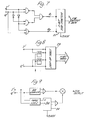
- In British patent application No. 8127797 (Serial No. 2106734A) there is described a direct conversion receiver incorporating a multi-mode digital demodulator, using the configuration shown in Fig. 1. In this receiver, the input signals from the antenna (or from the cable system or whatever) are mixed in two mixers 1, 2 with a
local oscillator 3. In either the oscillator or signal path a quadrature network is interposed 4 or 4' such that the relative phases of either the signal or the local oscillator have a phase difference of 900 at the two mixers. (As an alternative, two 450 phase shift networks of opposite sign may be used, one in the signal and one in the local oscillator). The outputs from the mixers are low-pass filtered 5,6 to select the difference frequency between the input signal and the local oscillator. Afteramplication 7,8 (if necessary) the signals in the two channels (termed the 'I' or in-phase and the 'Q' or quadrature channels) are converted from analogue todigital form 9, 10. The digital signals are processed in a digital signal processing block 11, which may consist of hardwired logic or which may be a microprocessor(s) programmed with software. The processor performs the demodulation of the signals and may also provide filtering and other post-detection functions. It further may provide specialised outputs such as feedback to the other receiver parts to control gain or phase - such feedback being either digital or converted to analogue via a digital to analogue converter. - The present invention provides for a simplified realisation of the digital processor demodulator using an approximation to the perfect system disclosed in the prior art and, inter alia, makes use of a particular form of analogue-to-digital converter. A demodulator for both amplitude and phase modulations is described, together with a number of variants to provide additional functions.
- According to the present invention there is provided a radio receiver having a first signal path in which a signal is mixed with a local oscillator frequency running at the main transmission frequency and then filtered to give a first mixed signal defined as an in-phase signal (I), a second signal path in which the received signal is mixed with the local oscillator frequency but with a relative phase shift and then filtered to give a second mixed signal defined as a quadrature signal (Q), characterised in that each signal path includes analogue-to-digital conversion means whereby the I and Q signals are converted into pulse density modulated (PDM) digital data streams respectively, the receiver also including a logic means to which the outputs of the PDM streams are applied, whereby the logic means output is a demodulation of the digital signals..
- Embodiments of the invention will now be described with reference to Figs. 2-9 of the accompanying drawings, in which:-
- Fig. 2 illustrates a demodulator arrangement according to the invention,
- Fig. 3 illustrates the principle of a delta-sigma modulator,
- Fig. 4 is a phasor diagram relating to the function of the circuitry of Fig. 2,
- Figs. 5 & 6 are further phasor diagrams,
- Fig. 7 illustrates an implementation of the demodulator logic of Fig. 1,
- Fig. 8 illustrates an alternative implementation of the demodulator logic, and
- Fig. 9 illustrates an implementation for 55B demodulation.
- In the arrangement shown in Fig. 2 the I and Q channels are separately digitised as single serial data streams using analogue-to-
digital converters 14, 15, which may be of the delta-sigma modulator type described OR Pulse Density Modulators as described in British patent 1450989. Fig. 3 shows the basic structure of such a modulator. The analogue input is compared with a reference voltage in comparator 20. The difference between the input and reference voltages sets the D input of aclocked bistable 21. The Q output of the bistable is applied in a negative feedback to the input. The outputs of the pulse density modulators are applied to alogic block 18.Logic block 18 produces a digital word output dependent on the states of the I & Q pulse density inputs. There may also be a clock input to theblock 18. The outputs are applied to a digital-to-analogue converter 19 when necessary, and smoothed using a low-pass filter which may consist simply of an RC section, or which may be a more complex filter. - The function of the circuitry may be seen with reference to Fig. 4 which shows a phasor diagram. The reference phase for this diagram is the local oscillator phase and the amplitudes of two channels are represented on the axes at right-angles. An input signal at any instant in time may be represented by a phasor as shown, having relative phase 8, and amplitude rl. Thus, for example, a frequency modulated signal would have constant amplitude and the phase would vary as the integral of the modulating information in the usual way. A continuous- wave carrier would be represented by a phasor which rotated at a constant speed either clock-wise or anticlockwise depending on whether it were higher or lower in frequency than the local oscillator.
- In the present case, the values of I or Q at the digital processor are constrained to be zero or one or a series of such digits since they are a digital data stream and we choose to represent all zeros at the left or bottom of the diagram and all ones at the right or top.

- The amplitude may be represented by any number of digits of the data streams and an approximation to the amplitude or phase decoded.
- For example, for one data bit at a time, the phase may clearly be deduced to be in one quadrant and assigned that value by the logic block as given in Table I.
- Since the phase values are binarily related to 900 increments, this phase can be represented by a two bit data output. A logic circuit to implement this is given in Figure 7.
- By subtracting one phase value from the previous phase value, the differential of the phase (i.e. the frequency) is demodulated. Thus, just as the inputs are estimated by an incremental digital stream, the demodulated outputs are also estimated. When these outputs are smoothed, an adequate approximation to the required demodulated information is obtained.
- While the approximations made above are accurate for phasors which truly lie in the 450 or 1350 positions etc, intermediate values are not so accurately demodulated, since they are formed as a linear approximation between the available outputs. The peak error in this process is half-way between the set values: for example, a phasor which actually would be represented by exact values of I equals unity and Q equals three quarters will be approximated as one half of 45°, that is, 22.50, whereas the correct output is arc tangent 0.5 which is 26.60. This is in fact the peak error and is clearly repeated at eight points around the phasor diagram and has a maximum value of about +4°. In many circumstances, this approximation is adequate. However, if greater fidelity is needed, then this can be provided by taking more than one sample of data at a time.
- Figs. 5 and 6 show the case where a pair of sequential samples of the I and Q data are used. Thus the left and bottom is '00' the right and top 'll' and a value of 0.5 assigned to the combinations '01' or '10' at the centre - ('01' and '10' have the same significance since each data sample has equal weight). Correct output values may now be assigned for the intermediate samples.
- Fig. 5 shows the phase outputs. In a similar fashion, Fig. 6 gives the amplitude values for the first quadrant, and Table II summarises the values for this case. Note that for the phase output the I=10, Q=10 case is undefined. In this case the output may be held at the previous value or an interpolation made between previous and subsequent values.
-

- In both of these cases, the output samples are only available at half the clock rate of the analogue-to-digital converters. However, this is more than compensated by the improved accuracy.
- Alternatively, the data from the 'one-bit' analogue-to-digital converter may be slipped through such that each bit is used twice and the output remains at the original clock sampling rate.
- Clearly, the principle may be extended to taking any number of bits of data at a time. It will also be clear that as the clock frequency is made higher, smaller analogue input signals can be demodulated with adequate resolution. That is, the dynamic range of the processor can be increased directly with the clock rate.
- The hardware needed for the
block 18 in Fig. 2 consists in essence of logic to implement either Table I or Table II as a truth table. Fig. 7 shows an exemplary implementation for the simplest case of the one-bit-at-a-time phase and frequency demodulator. In this case, the phase values have binary weights (i.e. 0, 45, 90) and can thus be directly assigned. The combinational logic shown is merely one possible way of achieving the function required. - For frequency demodulation the differential of the phase is required and this may be obtained by subtracting each phase output word from its predecessor. The
subtractor block 22 uses the clock input to time the storing of one word and its subtraction from the previous one. A 2-bit output (i.e. without the most-significant bit) is used. - To implement the amplitude values of Table I and the whole of Table II, outputs from the
processor block 18 are needed which do not have simple binary relationships. Two possibilities exist here: firstly, the correct values may be assigned at the point of digital-to-analogue conversion. Thus, the digital-to-analogue converter is provided with weighted outputs (set, for example, by the ratios of resistors or capacitors or the width of pulses, etc.) which have the values of 1, √2,
- The second method outputs a conventional binary weighted digital word of sufficient number of bits to describe the required values to any accuracy desired. Thus, to give a better than 1% accuracy, a 7-bit word is employed. However, only a small number of such words are needed (e.g. 3 for the two-bits-at-a-time amplitude demodulator, including all zeros and all ones as two of them). In this case, the simplest hardware form is a look-up table 23, Fig. 8, addressed with the I and Q values and outputting the appropriate word. This data word can now be further processed using conventional digital signal processing techniques.
- A number of other functions may also be needed in practical equipments. These may be derived from the fundamental data of phase and amplitude or will sometimes be more conveniently obtained directly. For example, for automatic gain control feedback, an output is needed which is derived from the square of the amplitude. This can be provided directly by (I2 + Q2). The result of this is compared with a threshold and a single bit output provided whenever the value is exceeded. Smoothing this value gives the analogue a.g.c. voltage. Table II gives the conversion values applicable to this case.
- Single-sideband demodulation requires a special configuration as given in patent application No. 8127797. The local oscillator is nominally placed in the centre of the sideband and the phase of the output samples then needs to be shifted at a rate which is the equivalent of the offset frequency from the originals (suppressed) carrier. Fig. 9 shows the required circuitry for the one-bit-at-a-time case. The phase is shifted by adding or subtracting a fixed number (depending on whether the signal is an upper or lower sideband) in the
phase logic 24.
Claims (4)
Applications Claiming Priority (2)
| Application Number | Priority Date | Filing Date | Title |
|---|---|---|---|
| GB8328949 | 1983-10-29 | ||
| GB08328949A GB2149244B (en) | 1983-10-29 | 1983-10-29 | Digital demodulator arrangement for quadrature signals |
Publications (2)
| Publication Number | Publication Date |
|---|---|
| EP0143539A2 true EP0143539A2 (en) | 1985-06-05 |
| EP0143539A3 EP0143539A3 (en) | 1987-06-24 |
Family
ID=10550943
Family Applications (1)
| Application Number | Title | Priority Date | Filing Date |
|---|---|---|---|
| EP84307025A Withdrawn EP0143539A3 (en) | 1983-10-29 | 1984-10-15 | Digital demodulator arrangement for quadrature signals |
Country Status (11)
| Country | Link |
|---|---|
| US (1) | US4583239A (en) |
| EP (1) | EP0143539A3 (en) |
| JP (1) | JPS60112344A (en) |
| AU (1) | AU562232B2 (en) |
| CA (1) | CA1235754A (en) |
| ES (1) | ES8606963A1 (en) |
| FI (1) | FI79430C (en) |
| GB (1) | GB2149244B (en) |
| HK (1) | HK18588A (en) |
| NO (1) | NO844289L (en) |
| NZ (1) | NZ209885A (en) |
Cited By (4)
| Publication number | Priority date | Publication date | Assignee | Title |
|---|---|---|---|---|
| EP0310796A1 (en) * | 1987-10-08 | 1989-04-12 | BBC Brown Boveri AG | FM-signal demodulation method |
| EP0335037A1 (en) * | 1988-03-26 | 1989-10-04 | Stc Plc | Direct conversion radio |
| EP0373517A2 (en) * | 1988-12-16 | 1990-06-20 | Motorola, Inc. | Digital automatic frequency control on pure sine waves |
| US8406270B2 (en) | 2005-02-17 | 2013-03-26 | Analog Devices, Inc. | Quadrature demodulation with phase shift |
Families Citing this family (42)
| Publication number | Priority date | Publication date | Assignee | Title |
|---|---|---|---|---|
| GB2155262B (en) * | 1984-03-01 | 1988-01-20 | Standard Telephones Cables Ltd | Radio receiver |
| US4731796A (en) * | 1984-10-25 | 1988-03-15 | Stc, Plc | Multi-mode radio transceiver |
| GB2192506B (en) * | 1986-07-12 | 1990-05-30 | Stc Plc | Demodulation circuit |
| US4825452A (en) * | 1987-03-04 | 1989-04-25 | National Semiconductor Corporation | Digital FSK demodulator |
| GB2219899A (en) * | 1988-06-17 | 1989-12-20 | Philips Electronic Associated | A zero if receiver |
| GB2220315A (en) * | 1988-07-01 | 1990-01-04 | Philips Electronic Associated | Signal amplitude-determining apparatus |
| US5396520A (en) * | 1992-07-29 | 1995-03-07 | Dial Page Lp | Digital RF receiver |
| GB9408759D0 (en) * | 1994-05-03 | 1994-06-22 | Texas Instruments Ltd | Using high level cad tools to design application specific standard products for tv sound decoder systems |
| US5579347A (en) * | 1994-12-28 | 1996-11-26 | Telefonaktiebolaget Lm Ericsson | Digitally compensated direct conversion receiver |
| JPH11504786A (en) * | 1996-02-29 | 1999-04-27 | フィリップス エレクトロニクス ネムローゼ フェンノートシャップ | Receiver for digitally processing phase-separated input signals |
| US6035005A (en) * | 1997-02-10 | 2000-03-07 | Motorola, Inc. | Receiver with baseband I and Q demodulator |
| US6061551A (en) | 1998-10-21 | 2000-05-09 | Parkervision, Inc. | Method and system for down-converting electromagnetic signals |
| US7515896B1 (en) * | 1998-10-21 | 2009-04-07 | Parkervision, Inc. | Method and system for down-converting an electromagnetic signal, and transforms for same, and aperture relationships |
| US6091940A (en) * | 1998-10-21 | 2000-07-18 | Parkervision, Inc. | Method and system for frequency up-conversion |
| US6694128B1 (en) | 1998-08-18 | 2004-02-17 | Parkervision, Inc. | Frequency synthesizer using universal frequency translation technology |
| US6542722B1 (en) | 1998-10-21 | 2003-04-01 | Parkervision, Inc. | Method and system for frequency up-conversion with variety of transmitter configurations |
| US6560301B1 (en) | 1998-10-21 | 2003-05-06 | Parkervision, Inc. | Integrated frequency translation and selectivity with a variety of filter embodiments |
| US6813485B2 (en) | 1998-10-21 | 2004-11-02 | Parkervision, Inc. | Method and system for down-converting and up-converting an electromagnetic signal, and transforms for same |
| US6370371B1 (en) | 1998-10-21 | 2002-04-09 | Parkervision, Inc. | Applications of universal frequency translation |
| US7039372B1 (en) | 1998-10-21 | 2006-05-02 | Parkervision, Inc. | Method and system for frequency up-conversion with modulation embodiments |
| US7236754B2 (en) | 1999-08-23 | 2007-06-26 | Parkervision, Inc. | Method and system for frequency up-conversion |
| US6049706A (en) * | 1998-10-21 | 2000-04-11 | Parkervision, Inc. | Integrated frequency translation and selectivity |
| US6061555A (en) | 1998-10-21 | 2000-05-09 | Parkervision, Inc. | Method and system for ensuring reception of a communications signal |
| EP1014637B1 (en) * | 1998-12-23 | 2006-05-03 | Asulab S.A. | Direct conversion receiver for FSK modulated signals |
| US6704558B1 (en) | 1999-01-22 | 2004-03-09 | Parkervision, Inc. | Image-reject down-converter and embodiments thereof, such as the family radio service |
| US6704549B1 (en) | 1999-03-03 | 2004-03-09 | Parkvision, Inc. | Multi-mode, multi-band communication system |
| US6879817B1 (en) | 1999-04-16 | 2005-04-12 | Parkervision, Inc. | DC offset, re-radiation, and I/Q solutions using universal frequency translation technology |
| US6853690B1 (en) * | 1999-04-16 | 2005-02-08 | Parkervision, Inc. | Method, system and apparatus for balanced frequency up-conversion of a baseband signal and 4-phase receiver and transceiver embodiments |
| US7065162B1 (en) * | 1999-04-16 | 2006-06-20 | Parkervision, Inc. | Method and system for down-converting an electromagnetic signal, and transforms for same |
| US7693230B2 (en) | 1999-04-16 | 2010-04-06 | Parkervision, Inc. | Apparatus and method of differential IQ frequency up-conversion |
| US7110444B1 (en) | 1999-08-04 | 2006-09-19 | Parkervision, Inc. | Wireless local area network (WLAN) using universal frequency translation technology including multi-phase embodiments and circuit implementations |
| US8295406B1 (en) | 1999-08-04 | 2012-10-23 | Parkervision, Inc. | Universal platform module for a plurality of communication protocols |
| CA2281236C (en) | 1999-09-01 | 2010-02-09 | Tajinder Manku | Direct conversion rf schemes using a virtually generated local oscillator |
| US7010286B2 (en) | 2000-04-14 | 2006-03-07 | Parkervision, Inc. | Apparatus, system, and method for down-converting and up-converting electromagnetic signals |
| US7454453B2 (en) | 2000-11-14 | 2008-11-18 | Parkervision, Inc. | Methods, systems, and computer program products for parallel correlation and applications thereof |
| US7072427B2 (en) * | 2001-11-09 | 2006-07-04 | Parkervision, Inc. | Method and apparatus for reducing DC offsets in a communication system |
| US7460584B2 (en) | 2002-07-18 | 2008-12-02 | Parkervision, Inc. | Networking methods and systems |
| US7379883B2 (en) | 2002-07-18 | 2008-05-27 | Parkervision, Inc. | Networking methods and systems |
| TWI280690B (en) * | 2003-03-18 | 2007-05-01 | Tdk Corp | Electronic device for wireless communications and reflector device for wireless communication cards |
| FR2873517B1 (en) * | 2004-07-20 | 2006-11-17 | Eads Telecom Soc Par Actions S | METHOD AND DEVICE FOR DIGITAL ANALOGUE CONVERSION WITH SYMMETRIC CORRECTION |
| FR2878667B1 (en) * | 2004-11-29 | 2007-08-24 | Eads Telecom Soc Par Actions S | METHOD AND DEVICE FOR DIGITAL ANALOG CONVERSION WITH DISSYMETRY CORRECTION |
| US7650084B2 (en) * | 2005-09-27 | 2010-01-19 | Alcatel-Lucent Usa Inc. | Optical heterodyne receiver and method of extracting data from a phase-modulated input optical signal |
Citations (6)
| Publication number | Priority date | Publication date | Assignee | Title |
|---|---|---|---|---|
| US3609555A (en) * | 1967-07-19 | 1971-09-28 | Ibm | Digital fm receiver |
| US3701948A (en) * | 1970-09-17 | 1972-10-31 | North American Rockwell | System for phase locking on a virtual carrier |
| US3955191A (en) * | 1974-03-05 | 1976-05-04 | International Standard Electric Corporation | Analog-to-digital converter |
| US4057759A (en) * | 1976-06-23 | 1977-11-08 | Gte Sylvania Incorporated | Communication receiving apparatus |
| EP0065805A1 (en) * | 1981-05-27 | 1982-12-01 | Koninklijke Philips Electronics N.V. | Receiver for angle-modulated carrier signals |
| EP0074858A2 (en) * | 1981-09-15 | 1983-03-23 | International Standard Electric Corporation | Radio receiver |
Family Cites Families (3)
| Publication number | Priority date | Publication date | Assignee | Title |
|---|---|---|---|---|
| US4090145A (en) * | 1969-03-24 | 1978-05-16 | Webb Joseph A | Digital quadrature demodulator |
| US3953805A (en) * | 1974-11-07 | 1976-04-27 | Texas Instruments Incorporated | DC component suppression in zero CF IF systems |
| US4509017A (en) * | 1981-09-28 | 1985-04-02 | E-Systems, Inc. | Method and apparatus for pulse angle modulation |
-
1983
- 1983-10-29 GB GB08328949A patent/GB2149244B/en not_active Expired
-
1984
- 1984-10-15 EP EP84307025A patent/EP0143539A3/en not_active Withdrawn
- 1984-10-15 NZ NZ209885A patent/NZ209885A/en unknown
- 1984-10-17 FI FI844092A patent/FI79430C/en not_active IP Right Cessation
- 1984-10-17 AU AU34444/84A patent/AU562232B2/en not_active Ceased
- 1984-10-18 US US06/662,050 patent/US4583239A/en not_active Expired - Fee Related
- 1984-10-19 CA CA000465960A patent/CA1235754A/en not_active Expired
- 1984-10-26 NO NO844289A patent/NO844289L/en unknown
- 1984-10-27 ES ES537156A patent/ES8606963A1/en not_active Expired
- 1984-10-29 JP JP59227625A patent/JPS60112344A/en active Pending
-
1988
- 1988-03-10 HK HK185/88A patent/HK18588A/en unknown
Patent Citations (6)
| Publication number | Priority date | Publication date | Assignee | Title |
|---|---|---|---|---|
| US3609555A (en) * | 1967-07-19 | 1971-09-28 | Ibm | Digital fm receiver |
| US3701948A (en) * | 1970-09-17 | 1972-10-31 | North American Rockwell | System for phase locking on a virtual carrier |
| US3955191A (en) * | 1974-03-05 | 1976-05-04 | International Standard Electric Corporation | Analog-to-digital converter |
| US4057759A (en) * | 1976-06-23 | 1977-11-08 | Gte Sylvania Incorporated | Communication receiving apparatus |
| EP0065805A1 (en) * | 1981-05-27 | 1982-12-01 | Koninklijke Philips Electronics N.V. | Receiver for angle-modulated carrier signals |
| EP0074858A2 (en) * | 1981-09-15 | 1983-03-23 | International Standard Electric Corporation | Radio receiver |
Non-Patent Citations (1)
| Title |
|---|
| IEEE TRANSACTIONS ON COMMUNICATIONS, vol. COM-28, no. 3, March 1980, pages 375-379; S.K. MULLICK "Noise study of an asynchronous delta sigma modulator" * |
Cited By (5)
| Publication number | Priority date | Publication date | Assignee | Title |
|---|---|---|---|---|
| EP0310796A1 (en) * | 1987-10-08 | 1989-04-12 | BBC Brown Boveri AG | FM-signal demodulation method |
| EP0335037A1 (en) * | 1988-03-26 | 1989-10-04 | Stc Plc | Direct conversion radio |
| EP0373517A2 (en) * | 1988-12-16 | 1990-06-20 | Motorola, Inc. | Digital automatic frequency control on pure sine waves |
| EP0373517A3 (en) * | 1988-12-16 | 1990-08-16 | Motorola, Inc. | Digital automatic frequency control on pure sine waves |
| US8406270B2 (en) | 2005-02-17 | 2013-03-26 | Analog Devices, Inc. | Quadrature demodulation with phase shift |
Also Published As
| Publication number | Publication date |
|---|---|
| FI844092L (en) | 1985-04-30 |
| ES8606963A1 (en) | 1986-05-16 |
| NO844289L (en) | 1985-04-30 |
| ES537156A0 (en) | 1986-05-16 |
| GB2149244B (en) | 1987-01-21 |
| CA1235754A (en) | 1988-04-26 |
| FI79430C (en) | 1989-12-11 |
| AU3444484A (en) | 1985-05-02 |
| FI79430B (en) | 1989-08-31 |
| NZ209885A (en) | 1988-07-28 |
| JPS60112344A (en) | 1985-06-18 |
| US4583239A (en) | 1986-04-15 |
| HK18588A (en) | 1988-03-18 |
| EP0143539A3 (en) | 1987-06-24 |
| FI844092A0 (en) | 1984-10-17 |
| GB8328949D0 (en) | 1983-11-30 |
| AU562232B2 (en) | 1987-06-04 |
| GB2149244A (en) | 1985-06-05 |
Similar Documents
| Publication | Publication Date | Title |
|---|---|---|
| US4583239A (en) | Digital demodulator arrangement for quadrature signals | |
| US5574755A (en) | I/Q quadraphase modulator circuit | |
| US5621345A (en) | In-phase and quadrature sampling circuit | |
| EP0400027B1 (en) | Method and apparatus for quadrature modulation | |
| JP3419484B2 (en) | Modulator, transmitter | |
| US4878029A (en) | Complex digital sampling converter for demodulator | |
| KR100221692B1 (en) | Transmitter with modified carrier signal generating electronic device | |
| US5473280A (en) | Modulation/demodulation method and system for realizing quadrature modulation/demodulation technique used in digital mobile radio system with complex signal processing | |
| US20040092240A1 (en) | Phase detection circuit and receiver | |
| CA1281080C (en) | Digital zero-if selectivity section | |
| EP0692867B1 (en) | FM modulation circuit and method | |
| US5295162A (en) | Digital demodulator which quantizes signal components according to different thresholds | |
| US4674105A (en) | Digital signal processor | |
| US5067140A (en) | Conversion of analog signal into i and q digital signals with enhanced image rejection | |
| EP0412291B1 (en) | Quadrature FSK receiver with compensation for frequency offset | |
| US5942955A (en) | Quasi-GMSK modulator | |
| US5586147A (en) | Demodulation method using quadrature modulation | |
| US4461011A (en) | Method and apparatus for converting binary information into a high density single-sideband signal | |
| KR100317322B1 (en) | Device of QPSK modulation using the Phase Compensator | |
| US6239666B1 (en) | Uniform amplitude modulator | |
| US5617063A (en) | Matched filters for processing related signal components | |
| US6563887B1 (en) | Direct conversion receiver for frequency-shift keying modulated signals | |
| AU642373B2 (en) | A digital quadrature phase detector for angle modulated signals | |
| US5623225A (en) | Quadrature signal demodulation using quantizing and accumulating | |
| AU660877B2 (en) | Differential detection demodulator |
Legal Events
| Date | Code | Title | Description |
|---|---|---|---|
| PUAI | Public reference made under article 153(3) epc to a published international application that has entered the european phase |
Free format text: ORIGINAL CODE: 0009012 |
|
| AK | Designated contracting states |
Designated state(s): AT BE CH DE FR IT LI LU NL SE |
|
| RAP1 | Party data changed (applicant data changed or rights of an application transferred) |
Owner name: STC PLC |
|
| RAP1 | Party data changed (applicant data changed or rights of an application transferred) |
Owner name: STC PLC |
|
| PUAL | Search report despatched |
Free format text: ORIGINAL CODE: 0009013 |
|
| AK | Designated contracting states |
Kind code of ref document: A3 Designated state(s): AT BE CH DE FR IT LI LU NL SE |
|
| 17P | Request for examination filed |
Effective date: 19871007 |
|
| 17Q | First examination report despatched |
Effective date: 19890724 |
|
| STAA | Information on the status of an ep patent application or granted ep patent |
Free format text: STATUS: THE APPLICATION IS DEEMED TO BE WITHDRAWN |
|
| 18D | Application deemed to be withdrawn |
Effective date: 19891205 |
|
| RIN1 | Information on inventor provided before grant (corrected) |
Inventor name: VANCE, IAN ALISTAIR WARD |