EP0143591A2 - Sense amplifier - Google Patents
Sense amplifier Download PDFInfo
- Publication number
- EP0143591A2 EP0143591A2 EP84308017A EP84308017A EP0143591A2 EP 0143591 A2 EP0143591 A2 EP 0143591A2 EP 84308017 A EP84308017 A EP 84308017A EP 84308017 A EP84308017 A EP 84308017A EP 0143591 A2 EP0143591 A2 EP 0143591A2
- Authority
- EP
- European Patent Office
- Prior art keywords
- transistor
- coupled
- current electrode
- amplifier
- bit line
- Prior art date
- Legal status (The legal status is an assumption and is not a legal conclusion. Google has not performed a legal analysis and makes no representation as to the accuracy of the status listed.)
- Withdrawn
Links
Images
Classifications
-
- G—PHYSICS
- G11—INFORMATION STORAGE
- G11C—STATIC STORES
- G11C11/00—Digital stores characterised by the use of particular electric or magnetic storage elements; Storage elements therefor
- G11C11/21—Digital stores characterised by the use of particular electric or magnetic storage elements; Storage elements therefor using electric elements
- G11C11/34—Digital stores characterised by the use of particular electric or magnetic storage elements; Storage elements therefor using electric elements using semiconductor devices
- G11C11/40—Digital stores characterised by the use of particular electric or magnetic storage elements; Storage elements therefor using electric elements using semiconductor devices using transistors
- G11C11/401—Digital stores characterised by the use of particular electric or magnetic storage elements; Storage elements therefor using electric elements using semiconductor devices using transistors forming cells needing refreshing or charge regeneration, i.e. dynamic cells
- G11C11/4063—Auxiliary circuits, e.g. for addressing, decoding, driving, writing, sensing or timing
- G11C11/407—Auxiliary circuits, e.g. for addressing, decoding, driving, writing, sensing or timing for memory cells of the field-effect type
-
- G—PHYSICS
- G11—INFORMATION STORAGE
- G11C—STATIC STORES
- G11C7/00—Arrangements for writing information into, or reading information out from, a digital store
- G11C7/06—Sense amplifiers; Associated circuits, e.g. timing or triggering circuits
- G11C7/065—Differential amplifiers of latching type
-
- G—PHYSICS
- G11—INFORMATION STORAGE
- G11C—STATIC STORES
- G11C11/00—Digital stores characterised by the use of particular electric or magnetic storage elements; Storage elements therefor
- G11C11/21—Digital stores characterised by the use of particular electric or magnetic storage elements; Storage elements therefor using electric elements
- G11C11/34—Digital stores characterised by the use of particular electric or magnetic storage elements; Storage elements therefor using electric elements using semiconductor devices
- G11C11/40—Digital stores characterised by the use of particular electric or magnetic storage elements; Storage elements therefor using electric elements using semiconductor devices using transistors
- G11C11/401—Digital stores characterised by the use of particular electric or magnetic storage elements; Storage elements therefor using electric elements using semiconductor devices using transistors forming cells needing refreshing or charge regeneration, i.e. dynamic cells
- G11C11/4063—Auxiliary circuits, e.g. for addressing, decoding, driving, writing, sensing or timing
- G11C11/407—Auxiliary circuits, e.g. for addressing, decoding, driving, writing, sensing or timing for memory cells of the field-effect type
- G11C11/409—Read-write [R-W] circuits
- G11C11/4091—Sense or sense/refresh amplifiers, or associated sense circuitry, e.g. for coupled bit-line precharging, equalising or isolating
-
- H—ELECTRICITY
- H03—ELECTRONIC CIRCUITRY
- H03F—AMPLIFIERS
- H03F3/00—Amplifiers with only discharge tubes or only semiconductor devices as amplifying elements
Definitions
- This invention relates to sense amplifiers, and more particularly, to clocked sense amplifiers for use in a memory which has bit line pairs.
- a typical differential amplifier is a cross-coupled pair of transistors. The offset in such a case is from two major causes which can appear together or independently. One major cause is threshold voltage differential between the two transistors. The other major cause is gain differential between the two transistors. The cause of gain differential is typically effective gate length differential.
- gains and threshold voltages vary substantially from one chip to another due to processing variations, gains and threshold voltages are matched quite closely on a given chip. Nonetheless, there is some variation even on the same chip. As the number of sense amplifiers increase as the density increases, the probability of there being enough gain and/or threshold voltage variation to cause an offset failure on at least one sense amplifier increases.
- One technique to reduce failures due to offset is to enable the cross-coupled amplifier relatively slowly. This is to avoid having large current flow. Large current flow amplifies the offset problem for the case of threshold voltage differential.
- Another variation of this approach is to enable the cross-coupled pair with a weak transistor which provides significant current limiting, then subsequently enabling the cross-coupled pair with a much higher gain transistor. These approaches are useful but do not provide much help for the gain differential situation.
- the amplifier feeds back to the bit lines. This is typically necessary to restore data in the selected storage cell.
- the sense amplifier is expected to be able to detect a voltage differential of 75 millivolts on the bit lines. For the case in which the amplifier has minimal offset, the amplifier senses the voltage differential on the bit lines and begins to further increase the voltage differential. In the case where there is significant offset, the amplifier may actually begin pulling the bit lines closer together in voltage. Once this begins the amplifier will eventually cause the voltage on the bit lines to cross-over and reverse the data. This failure mode is the kind that can occur to a single sense amplifier on the chip while there are no other failures on the chip.
- An object of the invention is to provide an improved sense amplifier.
- Another object of the invention is to provide a sense amplifier with reduced probability of failure.
- Yet another object of the invention is to provide a sense amplifier with improved offset immunity.
- a sense amplifier which has a first differential amplifier and a second differential amplifier coupled to a pair of bit lines.
- the first differential amplifier is enabled by a first signal.
- the second differential amplifier is enabled a preaetermined time duration following the occurrence of the first signal.
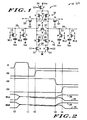
- FIG. 1 Shown in FIG. 1 is a portion of a dynamic random access memory (DRAM) 10 comprised generally of a sense amplifier 11, a storage cell 12, a storage cell 13, a storage cell 14, and a storage cell 15.
- Sense amplifier 11 is comprised of a P channel cross-coupled differential amplifier 18, an N channel cross-coupled differential amplifier 19, an N channel coupling transistor 20, an N channel coupling transistor 21, an N channel enabling transistor 22, an N channel enabling transistor 23, a P channel enabling transistor 24, and an N channel coupling transistor 25.
- Amplifier 18 comprises a P channel transistor 26 and a P channel transistor 27.
- Amplifier 19 comprises an N channel transistor 28 and an N channel transistor 29.
- Storage cells 12-15 use P channel pass transistors. Although N channel pass transistors have been commonly used in DRAMs, P channel storage cells 12-15 are well known in the art.
- P channel transistors 24, 26, and 27 are enhancement mode, P channel insulated gate field effect transistors with a threshold voltage of -0.6 to -0.9 volt.
- N channel transistors 22, 23, 25, 28, and 29 are enhancement mode, N channel insulated gate field effect transistors having a threshold voltage of 0.6 to 0.9 volt.
- Storage cells 14 and 15 are coupled between a bit line 35 and a positive power supply terminal V cc for receiving a positive power supply voltage, for example 5 volts. Storage cells 14 and 15 are enabled in response to receiving signals on word lines WL1 and WL2, respectively. Storage cells 12 and 13 are coupled between a bit line 36 and V CC , and are enabled in response to receiving signals on word lines WL3 and WL4, respectively. Sense amplifier 11 is coupled to pair of bit lines 35 and 36 for detecting a differential voltage therebetween.
- storage cells 12-15 store a logic high or a logic low.
- one of storage cells 12-15 When one of storage cells 12-15 is enabled it provides a voltage deviation, which corresponds to the stored logic state, from the bias level on the bit line (35 or 36) to which it is coupled.
- a stored logic high will cause an increase in voltage whereas a logic low will cause a decrease in voltage.
- bit line 36 If a storage cell on bit line 35 is enabled, then no storage cell on the opposite bit line, bit line 36, will be enabled. Consequently, bit line 36 provides a bias level which is approximately halfway between the voltage level of a logic high and a logic low. Regardless of the logic state of the storage cell on bit line 35, there is a voltage differential established between bit lines 35 and 36 for sense amplifier 11 to detect.
- SRAM static random access memory
- each storage cell provides a pair of outputs to a pair of bit lines for establishing a voltage differential for detection by a sense amplifier.
- ROM read only memory
- Sense amplifier 11 has a node 37 connected to bit line 36 and a node 38 connected to bit line 35.
- Transistor 29 has a drain connected to node 38, a gate connected to node 37, and a source connected to a node 39.
- Transistor 28 has a drain connected to node 37, a gate connected to node 38, and a source connected to node 39.
- Transistor 22 has a drain connected to node 39, a source connected to ground, and a gate for receiving a clock signal C1.
- Transistor 23 has a drain connected to node 39, a source connected to ground, and a gate for receiving a clock signal C3.
- Transistor 27 has a drain connected to node 38, a source connected to a node 41, and a gate connected to node 37.
- Transistor 26 has a drain connected to node 37, a source connected to node 41, and a gate connected to node 38.
- Transistor 24 has a drain connected to node 41, a source connected to V cc , and a gate for receiving a clock signal C2.
- Transistor 25 has a first current electrode connected to node 37, a second current electrode connected to node 38, and a control electrode for receiving a precharge signal P.
- Transistor 25 is for equalizing the voltage on bit lines 35 and 36 during a precharge cycle. The first and second current electrodes will vary as to functioning as a source or drain.
- Transistor 20 has a first current electrode connected to node 38, a control electrode for receiving a column decoder signal CD, and a second current electrode.
- Transistor 21 has a first current electrode conected to node 37, a control electrode for receiving column decoder signal CD, and a second current electrode.
- the second current electrodes of transistors 20 and 21 are connected to read/write circuitry (not shown) of the memory, typically via bit sense common lines. Data is coupled into or out of sense amplifier 11 when signal CD is present which is responsive to column decoding.
- sense amplifier 11 The primary advantages of sense amplifier 11 are when data is sensed as distinguished from written. In a DRAM storage cells must be refreshed periodically which requires sensing. In the write mode only one column is selected for writing while all other columns must be involved in refreshing. It is to be understood that in a memory there would be additional bit line pairs coupled to other sense amplifiers than those shown in FIG. 1, and that there would be additional storage cells coupled to bit lines 35 and 36 than those shown in FIG. 1.
- sense amplifier 11 Operation of sense amplifier 11 is explained in conjunction with signals shown in FIG. 2.
- precharge signal P switches to a logic high causing transistor 25 to equalize the voltage on bit lines 35 and-36 during the precharge cycle.
- the precharge period terminates with signal P switching to a logic low, turning off transistor 25.
- clock signals C1 and C3 are a logic low and signal C2 is a logic high, ensuring that transistors 22, 23 and 24 are turned off. With transistors 23, 24, and 25 turned off, amplifiers 18 and 19 are disabled.
- Case BL1 is the typical case when cross-coupled amplifier 19 does not have a significant offset.
- a storage cell When a storage cell is enabled, no storage cell on the opposite bit line is enabled. For example, storage cell 12 is enabled, but no storage cell coupled to bit line 35 is enabled. Regardless of the logic state of storage cell 12, there will be a voltage differential between bit lines 35 and 36, i.e., bit lines 35 and 36 will separate. The separation is nominally 200 millivolts but can be expected to be as low as 75 millivolts or even lower. Accordingly, the design goal for detection by a sense amplifier with significant offset was chosen to be 75 millivolts.
- clock signal C1 enables amplifier 19 for the purpose of amplifying the voltage differential on bit lines 35 and 36 and cause them to separate further. This is achieved by clock signal C1 switching to a logic high at time t 2 to turn on transistor 22.
- Transistor 22 is of relatively low gain so that node 39 does not quickly reach ground potential. Because of this relatively high resistance of transistor 22, amplifier 19 does not cause a rapid separation of bit lines 35 and 36. Although at this time both transistors 28 and 29 are conducting, one is receiving a higher gate voltage so that it is more conductive.
- node 37 will be at a higher voltage than node 38 in which case transistor 29 will be more conductive than transistor 28. This will cause node 38 to drop in voltage faster than node 37, thereby increasing the voltage differential between bit line 35 and 36.
- clock C2 enables amplifier 18 by switching to a logic low which turns on transistor 24.
- Transistor 24 has a higher gain than transistor 22 so that node 41 approaches the voltage at V cc faster than node 39 approached ground between times t 2 and t 3 .
- a principle ot cross-couplea amplifiers is that the gain thereof increases with voltage differential. Consequently, in case BL1 of bit lines 35 and 36 shown in FIG. 2, amplifier 19 amplifies the voltage differential between bit lines 35 and 36 from time t 2 to time t 3 . Even if amplifier 18 had a sufficiently high offset problem to be unable to amplify a 75 millivolt bit line differential or even worse if the offset would actually cause amplifier 18 to have some negative gain at a 75 millivolt bit line differential, the additional separation caused by amplifier 19 from time t 2 to time t 3 will be sufficient for amplifier 19 to have positive gain so that the voltage differential between bit lines 35 and 36 will be significantly increased.
- clock signal C3 turns on transistor 23 to pull node 39 to ground potential. This allows the bit line at the logic low to reach ground potential more rapidly, in this case bit line 35. This also helps bit line 36 reach the voltage at V . , because transistor 28 is consequently turned completely off. It is important that the bit lines reach the voltage at the power supply terminals, ground and V cc as appropriate, for refresh purposes as well as for subsequent equalization of bit lines 35 and 36 during the precharge cycle.
- amplifier 19 is assumed to have relatively significant offset.
- the circuit responds the same way as for case BL1 until time t 2 .
- amplifier 19 is enabled in response to clock C1 as in case BL1 but amplifier 18, due to offset, does not cause a further separation of bit lines 35 and 36.
- node 37 will be at a higher voltage than node 38.
- the offset which causes problems in this context is caused by transistor 29 having a lower gain than transistor 28 and transistor 29 having a higher threshold voltage than transistor 28. In one embodiment, it was assumed there could be a 50 millivolt threshold voltage variation and 10% gain differential.
- Transistor 22 was chosen to be of sufficiently low gain that the voltage differential would deteriorate to no less than 50 millivolts from time t 2 to time t 3 .
- amplifier 18 would be enabled by clock signal C2 switching to a logic low. In this case, amplifier 18 is assumed to have very little offset. Consequently, amplifier 18 amplifies the voltage differential between bit lines 35 and 36. Because transistor 24 is of relatively high gain, bit lines 35 and 36 separate more rapidly than between times t 2 and t 3 for case BL1.
- clock signal C3 enables transistor 23 at time t 4 there is already substantial bit line separation so that the bit lines are quickly pulled to the voltages at V cc and ground as appropriate.
- both amplifiers 18 and 19 have significant offset there may well be a failure. That both amplifiers would have significant offset is very unlikely because the offsets are independent of each other.
- the cause of offset for N channel amplifier 19 is substantially independent of the cause of offset of P channel amplifier 18. Additionally, the offsets would have to be in the same direction, i.e., the offset causes the amplifier to favor one logic state of a bit line over another. If the offsets of amplifiers 18 and 19 favored opposing logic states, there would not be a failure unless of course one of the offsets was extraordinarily severe in which case there would be a failure anyway.
- bit line separation would actually be greater between times t 2 and t 3 than for case BL1. Consequently, amplifier 18 would have even less difficulty in further amplifying the bit line voltage differential than in case BL1. Conversely if amplifier 19 favored node 37 at a logic low, but amplifier 18 favored node 37 at a logic high, the bit line separation between times t 2 and t 3 would be like case BL2. At time t 3 amplifier 18 would have even less difficulty, due to its offset favoring node 37 at a logic high, than in case BL2 in amplifying the bit line separation.
- amplifier 18 could also be enabled first with subsequent enabling of amplifier 19. In such a case amplifier 18 would be double clocked instead of amplifier 19 being double clocked.
- Another area of design choice is whether to have separate clocking transistors for each sense amplifier or have one transistor for many or even all of the sense amplifiers. Transistors 22, 23, and 24 could provide the necessary clocking for many sense amplifiers. In the particular embodiment chosen, each sense amplifier had a transistor analogous to transistor 24, whereas transistors 22 and 23 were common to many sense amplifiers. Typical considerations for this design choice are wave shaping, capacitive coupling and loading, and chip area.
Abstract
A sense amplifier (11) is coupled to a pair of bit lines (35, 36) for detecting and amplifying a voltage differential therebetween. The sense amplifier (10) has a first differential amplifier (18) coupled to the pair of bit lines (35, 36) enabled in response to a first signal. The sense amplifier also has a second differential amplifier (19) coupled to the pair of bit lines (35, 36) which is enabled a predetermined time duration following the occurrence of the first signal.
Description
- This invention relates to sense amplifiers, and more particularly, to clocked sense amplifiers for use in a memory which has bit line pairs.
- As memories become more and more dense, not only are there more memory cells, there are also more sense amplifiers, decoders, address buffers and other circuitry necessary for the operation of the memory. Consequently for a given probability of a failure of a single circuit type, the more of the circuit type that is present, the more likely the memory device will contain a failure, making the whole device defective. One approach is to use redundancy techniques. This of course requires additional chip area as well as requiring repair time and repair equipment which can be very expensive. Another approach is to reduce the probability of one of the circuit elements being a failure.
- In the case of sense amplifiers, the failure mode of most concern is offset of the differential amplifier. Of course other defects can cause sense amplifier failure as well, but these other defects will likely be evident at other locations on the memory chip, causing other failures. Offset of the differential amplifier can be from causes which do not result in failures anywhere else on the chip. Consequently, it is particularly desirable to avoid sense amplifier failure due to offset. A typical differential amplifier is a cross-coupled pair of transistors. The offset in such a case is from two major causes which can appear together or independently. One major cause is threshold voltage differential between the two transistors. The other major cause is gain differential between the two transistors. The cause of gain differential is typically effective gate length differential. Although gains and threshold voltages vary substantially from one chip to another due to processing variations, gains and threshold voltages are matched quite closely on a given chip. Nonetheless, there is some variation even on the same chip. As the number of sense amplifiers increase as the density increases, the probability of there being enough gain and/or threshold voltage variation to cause an offset failure on at least one sense amplifier increases.
- One technique to reduce failures due to offset is to enable the cross-coupled amplifier relatively slowly. This is to avoid having large current flow. Large current flow amplifies the offset problem for the case of threshold voltage differential. Another variation of this approach is to enable the cross-coupled pair with a weak transistor which provides significant current limiting, then subsequently enabling the cross-coupled pair with a much higher gain transistor. These approaches are useful but do not provide much help for the gain differential situation.
- In a cross-coupled pair sense amplifier, the amplifier feeds back to the bit lines. This is typically necessary to restore data in the selected storage cell. The sense amplifier is expected to be able to detect a voltage differential of 75 millivolts on the bit lines. For the case in which the amplifier has minimal offset, the amplifier senses the voltage differential on the bit lines and begins to further increase the voltage differential. In the case where there is significant offset, the amplifier may actually begin pulling the bit lines closer together in voltage. Once this begins the amplifier will eventually cause the voltage on the bit lines to cross-over and reverse the data. This failure mode is the kind that can occur to a single sense amplifier on the chip while there are no other failures on the chip.
- An object of the invention is to provide an improved sense amplifier.
- Another object of the invention is to provide a sense amplifier with reduced probability of failure.
- Yet another object of the invention is to provide a sense amplifier with improved offset immunity.
- These and other objects of the invention are provided in a sense amplifier which has a first differential amplifier and a second differential amplifier coupled to a pair of bit lines. The first differential amplifier is enabled by a first signal. The second differential amplifier is enabled a preaetermined time duration following the occurrence of the first signal.
-
- FIG. 1 is a schematic diagram of a portion of a dynamic random access memory which includes a sense amplifier according to a preferred embodiment of the invention; and
- FIG. 2 is a timing diagram of signals relevant to the memory of FIG. 1 and useful in understanding the preferred embodiment of the invention.
- Shown in FIG. 1 is a portion of a dynamic random access memory (DRAM) 10 comprised generally of a
sense amplifier 11, astorage cell 12, astorage cell 13, astorage cell 14, and astorage cell 15.Sense amplifier 11 is comprised of a P channel cross-coupleddifferential amplifier 18, an N channel cross-coupleddifferential amplifier 19, an Nchannel coupling transistor 20, an Nchannel coupling transistor 21, an Nchannel enabling transistor 22, an Nchannel enabling transistor 23, a Pchannel enabling transistor 24, and an Nchannel coupling transistor 25.Amplifier 18 comprises aP channel transistor 26 and aP channel transistor 27.Amplifier 19 comprises anN channel transistor 28 and anN channel transistor 29. - Storage cells 12-15 use P channel pass transistors. Although N channel pass transistors have been commonly used in DRAMs, P channel storage cells 12-15 are well known in the art.
P channel transistors N channel transistors -
Storage cells bit line 35 and a positive power supply terminal Vcc for receiving a positive power supply voltage, for example 5 volts.Storage cells Storage cells bit line 36 and VCC, and are enabled in response to receiving signals on word lines WL3 and WL4, respectively.Sense amplifier 11 is coupled to pair ofbit lines - In conventional fashion storage cells 12-15 store a logic high or a logic low. When one of storage cells 12-15 is enabled it provides a voltage deviation, which corresponds to the stored logic state, from the bias level on the bit line (35 or 36) to which it is coupled. A stored logic high will cause an increase in voltage whereas a logic low will cause a decrease in voltage. If a storage cell on
bit line 35 is enabled, then no storage cell on the opposite bit line,bit line 36, will be enabled. Consequently,bit line 36 provides a bias level which is approximately halfway between the voltage level of a logic high and a logic low. Regardless of the logic state of the storage cell onbit line 35, there is a voltage differential established betweenbit lines sense amplifier 11 to detect. Although dummy cell techniques are more common, this technique is well known in the art. The situation is much the same for a static random access memory (SRAM) as well. In a SRAM each storage cell provides a pair of outputs to a pair of bit lines for establishing a voltage differential for detection by a sense amplifier. In the case of a read only memory (ROM) in which the storage cell has only one output, much the same technique as for DRAMs can be used for establishing a voltage differential on a pair of bit lines for detection by a sense amplifier. -
Sense amplifier 11 has anode 37 connected to bitline 36 and anode 38 connected to bitline 35.Transistor 29 has a drain connected tonode 38, a gate connected tonode 37, and a source connected to anode 39.Transistor 28 has a drain connected tonode 37, a gate connected tonode 38, and a source connected tonode 39.Transistor 22 has a drain connected tonode 39, a source connected to ground, and a gate for receiving a clock signal C1.Transistor 23 has a drain connected tonode 39, a source connected to ground, and a gate for receiving a clock signal C3.Transistor 27 has a drain connected tonode 38, a source connected to anode 41, and a gate connected tonode 37.Transistor 26 has a drain connected tonode 37, a source connected tonode 41, and a gate connected tonode 38.Transistor 24 has a drain connected tonode 41, a source connected to Vcc, and a gate for receiving a clock signal C2.Transistor 25 has a first current electrode connected tonode 37, a second current electrode connected tonode 38, and a control electrode for receiving a prechargesignal P. Transistor 25 is for equalizing the voltage onbit lines Transistor 20 has a first current electrode connected tonode 38, a control electrode for receiving a column decoder signal CD, and a second current electrode.Transistor 21 has a first current electrode conected tonode 37, a control electrode for receiving column decoder signal CD, and a second current electrode. The second current electrodes oftransistors sense amplifier 11 when signal CD is present which is responsive to column decoding. - The primary advantages of
sense amplifier 11 are when data is sensed as distinguished from written. In a DRAM storage cells must be refreshed periodically which requires sensing. In the write mode only one column is selected for writing while all other columns must be involved in refreshing. It is to be understood that in a memory there would be additional bit line pairs coupled to other sense amplifiers than those shown in FIG. 1, and that there would be additional storage cells coupled tobit lines - Operation of
sense amplifier 11 is explained in conjunction with signals shown in FIG. 2. At a time t0, precharge signal P switches to a logichigh causing transistor 25 to equalize the voltage onbit lines 35 and-36 during the precharge cycle. At a time t1 after bit lines 35 and 36 have equalized, the precharge period terminates with signal P switching to a logic low, turning offtransistor 25. During the precharge cycle, clock signals C1 and C3 are a logic low and signal C2 is a logic high, ensuring thattransistors transistors amplifiers bit lines bit lines cross-coupled amplifier 19 does not have a significant offset. When a storage cell is enabled, no storage cell on the opposite bit line is enabled. For example,storage cell 12 is enabled, but no storage cell coupled tobit line 35 is enabled. Regardless of the logic state ofstorage cell 12, there will be a voltage differential betweenbit lines bit lines storage cell 12, clock signal C1 enablesamplifier 19 for the purpose of amplifying the voltage differential onbit lines transistor 22.Transistor 22 is of relatively low gain so thatnode 39 does not quickly reach ground potential. Because of this relatively high resistance oftransistor 22,amplifier 19 does not cause a rapid separation ofbit lines transistors storage cell 12,node 37 will be at a higher voltage thannode 38 in whichcase transistor 29 will be more conductive thantransistor 28. This will causenode 38 to drop in voltage faster thannode 37, thereby increasing the voltage differential betweenbit line amplifier 18 by switching to a logic low which turns ontransistor 24.Transistor 24 has a higher gain thantransistor 22 so thatnode 41 approaches the voltage at Vcc faster thannode 39 approached ground between times t2 and t3. Whenamplifier 18 is enabled, the bit lines have separated sufficiently that, even ifamplifier 18 has significant offset, the bit lines will be separated even further. A principle ot cross-couplea amplifiers is that the gain thereof increases with voltage differential. Consequently, in case BL1 ofbit lines amplifier 19 amplifies the voltage differential betweenbit lines amplifier 18 had a sufficiently high offset problem to be unable to amplify a 75 millivolt bit line differential or even worse if the offset would actually causeamplifier 18 to have some negative gain at a 75 millivolt bit line differential, the additional separation caused byamplifier 19 from time t2 to time t3 will be sufficient foramplifier 19 to have positive gain so that the voltage differential betweenbit lines - About 5 nanoseconds after time t3 at time t4, clock signal C3 turns on
transistor 23 to pullnode 39 to ground potential. This allows the bit line at the logic low to reach ground potential more rapidly, in this case bitline 35. This also helpsbit line 36 reach the voltage at V., becausetransistor 28 is consequently turned completely off. It is important that the bit lines reach the voltage at the power supply terminals, ground and Vcc as appropriate, for refresh purposes as well as for subsequent equalization ofbit lines - For case BL2 for
bit lines amplifier 19 is assumed to have relatively significant offset. The circuit responds the same way as for case BL1 until time t2. At time t2 amplifier 19 is enabled in response to clock C1 as in case BL1 butamplifier 18, due to offset, does not cause a further separation ofbit lines storage cell 12 is enabled and stores a logic high,node 37 will be at a higher voltage thannode 38. The offset which causes problems in this context is caused bytransistor 29 having a lower gain thantransistor 28 andtransistor 29 having a higher threshold voltage thantransistor 28. In one embodiment, it was assumed there could be a 50 millivolt threshold voltage variation and 10% gain differential.Transistor 22 was chosen to be of sufficiently low gain that the voltage differential would deteriorate to no less than 50 millivolts from time t2 to time t3. At time t3 amplifier 18 would be enabled by clock signal C2 switching to a logic low. In this case,amplifier 18 is assumed to have very little offset. Consequently,amplifier 18 amplifies the voltage differential betweenbit lines transistor 24 is of relatively high gain,bit lines transistor 23 at time t4 there is already substantial bit line separation so that the bit lines are quickly pulled to the voltages at Vcc and ground as appropriate. - In the case where both
amplifiers N channel amplifier 19 is substantially independent of the cause of offset ofP channel amplifier 18. Additionally, the offsets would have to be in the same direction, i.e., the offset causes the amplifier to favor one logic state of a bit line over another. If the offsets ofamplifiers amplifier 19 favorednode 37 at a logic high butamplifier 18 favorednode 37 at a logic low, bit line separation would actually be greater between times t2 and t3 than for case BL1. Consequently,amplifier 18 would have even less difficulty in further amplifying the bit line voltage differential than in case BL1. Conversely ifamplifier 19 favorednode 37 at a logic low, butamplifier 18 favorednode 37 at a logic high, the bit line separation between times t2 and t3 would be like case BL2. At time t3 amplifier 18 would have even less difficulty, due to its offset favoringnode 37 at a logic high, than in case BL2 in amplifying the bit line separation. - It should be pointed out that
amplifier 18 could also be enabled first with subsequent enabling ofamplifier 19. In such acase amplifier 18 would be double clocked instead ofamplifier 19 being double clocked. Another area of design choice is whether to have separate clocking transistors for each sense amplifier or have one transistor for many or even all of the sense amplifiers.Transistors transistor 24, whereastransistors
Claims (10)
1. A sense amplifier coupled to a pair of bit lines for sensing and amplifying a voltage differential between the pair of bit lines, comprising:
a first cross-coupled transistor amplifier coupled to the pair of bit lines enabled in response to a first signal;
a first transistor having a first current electrode coupled to a first bit line of the pair of bit lines, a control electrode coupled to a second bit line of the pair of bit lines, and a second current electrode;
a second transistor having a first current electrode coupled to the second bit line, a control electrode coupled to the first bit line, and a second current electrode coupled to the second current electrode of the first transistor; and
a third transistor having a first current electrode coupled to the second current electrodes of the first and second transistors, a control electrode for receiving a second signal, and a second current electrode coupled to a first power supply terminal.
2. The sense amplifier of claim 1 wherein the first amplifier comprises:
a fourth transistor having a first current electrode coupled to the first bit line, a control electrode coupled to the second bit line, and a second current electrode;
a fifth transistor having a first current electrode coupled to the second bit line, a control electrode coupled to the first bit line, and a second current electrode coupled to the second current electrode of the fourth transistor; and a sixth transistor having a first current electrode coupled to the second current electrodes of the fourth and fifth transistors, a control electrode for receiving the first signal, and a second current electrode coupled to a second power supply terminal.
3. The sense amplifier of claim 2 wherein the first, second, and third transistors are N channel transistors, and the fourth, fifth, and sixth transistors are P channel transistors.
4. The sense amplifier of claim 3 further comprising a seventh transistor having a first current electrode coupled to the first current electrode of the third transistor, a control electroae for receiving a third signal, and a second current electrode coupled to the first power supply terminal.
5. The sense amplifier of claim 4 wherein the seventh transistor is an N channel transistor.
6. The sense amplifier of claim 5 wherein the third, sixth, and seventh transistors each have a gain, the gain of the seventh transistor being greater than the gain of the sixth transistor, and the gain of the sixth transistor being greater than the gain of the third transistor.
7. In a sense amplifier having a first and a second differential amplifier, each coupled to a pair of bit lines for amplifying a voltage differential therebetween, a method comprising the steps of:
enabling the first differential amplifier; and enabling the second differential amplifier a
predetermined time duration following the enabling of the first differential amplifier.
8. A sense amplifier coupled to a pair of bit lines for sensing and amplifying a voltage differential between the pair of bit lines, comprising:
a first differential amplifier coupled to the pair of bit lines enabled in response to a first signal; and
a second differential amplifier coupled to the pair of bit lines enabled a predetermined time duration following the first signal.
9. The sense amplifier of claim 8 wherein the first amplifier comprises:
a first transistor having a first current electrode coupled to a first bit line of the pair of bit lines, a control electrode coupled to a second bit line of the pair of bit lines, and a second current electrode;
a second transistor having a first current electrode coupled to the second bit line, a control electrode coupled to the first bit line, and a second current electrode coupled to the second current electrode of the first transistor; and
a third transistor having a first current electrode coupled to the second current electrodes of the first and second transistors, a control electrode for receiving the first signal, and a second current electrode coupled to a first power supply terminal.
10. The sense amplifier of claim 9 wherein the second amplifier comprises:
a fourth transistor having a first current electrode coupled to the first bit line, a control electrode coupled to the second bit line, and a second current electrode;
a fifth transistor having a first current electrode coupled to the second bit line, a control electroce coupled to the first bit line, and a second current electrode coupled to the second current electrode of the fourth transistor; and
a sixth transistor having a first current electrode coupled to the second current electrodes of the fourth and fifth transistors, a control electrode for receiving a second signal which occurs at the predetermined time duration following the first signal, and a second current electrode coupled to a second power supply terminal.
Applications Claiming Priority (2)
| Application Number | Priority Date | Filing Date | Title |
|---|---|---|---|
| US06/554,517 US4551641A (en) | 1983-11-23 | 1983-11-23 | Sense amplifier |
| US554517 | 1983-11-23 |
Publications (2)
| Publication Number | Publication Date |
|---|---|
| EP0143591A2 true EP0143591A2 (en) | 1985-06-05 |
| EP0143591A3 EP0143591A3 (en) | 1988-01-07 |
Family
ID=24213672
Family Applications (1)
| Application Number | Title | Priority Date | Filing Date |
|---|---|---|---|
| EP84308017A Withdrawn EP0143591A3 (en) | 1983-11-23 | 1984-11-20 | Sense amplifier |
Country Status (4)
| Country | Link |
|---|---|
| US (1) | US4551641A (en) |
| EP (1) | EP0143591A3 (en) |
| JP (1) | JPS60136993A (en) |
| KR (1) | KR850003614A (en) |
Cited By (13)
| Publication number | Priority date | Publication date | Assignee | Title |
|---|---|---|---|---|
| EP0182457A2 (en) * | 1984-11-19 | 1986-05-28 | THORN EMI North America Inc. | A dynamic random access memory circuit and a method of stabilizing current surges in such a memory circuit |
| EP0185451A2 (en) * | 1984-12-13 | 1986-06-25 | Kabushiki Kaisha Toshiba | Semiconductor memory device with sense amplifiers |
| EP0205294A2 (en) * | 1985-06-03 | 1986-12-17 | Advanced Micro Devices, Inc. | Sense amplification scheme for an integrated circuit |
| EP0209051A2 (en) * | 1985-07-08 | 1987-01-21 | Nec Corporation | Sense amplifier circuit |
| EP0238180A1 (en) * | 1986-02-07 | 1987-09-23 | Advanced Micro Devices, Inc. | High gain sense amplifier for small current differential |
| EP0244628A1 (en) * | 1986-03-31 | 1987-11-11 | Kabushiki Kaisha Toshiba | Sense amplifier for a semiconductor memory device |
| FR2603414A1 (en) * | 1986-08-29 | 1988-03-04 | Bull Sa | READING AMPLIFIER |
| EP0306519A1 (en) * | 1987-03-09 | 1989-03-15 | Inmos Corp | Current sensing differential amplifier. |
| EP0350860A2 (en) * | 1988-07-11 | 1990-01-17 | Kabushiki Kaisha Toshiba | Semiconductor memory having improved sense amplifiers |
| EP0417973A2 (en) * | 1989-09-12 | 1991-03-20 | Kabushiki Kaisha Toshiba | Amplifier circuit having two inverters |
| US5293515A (en) * | 1989-09-12 | 1994-03-08 | Kabushiki Kaisha Toshiba | Amplifier circuit having two inverters |
| GB2308706A (en) * | 1995-12-29 | 1997-07-02 | Hyundai Electronics Ind | High speed sense amplifier for a semiconductor memory device |
| EP0798732A1 (en) * | 1996-03-29 | 1997-10-01 | STMicroelectronics S.r.l. | Gain modulated sense amplifier, particularly for memory devices |
Families Citing this family (38)
| Publication number | Priority date | Publication date | Assignee | Title |
|---|---|---|---|---|
| FR2528613B1 (en) * | 1982-06-09 | 1991-09-20 | Hitachi Ltd | SEMICONDUCTOR MEMORY |
| USRE34026E (en) * | 1984-08-02 | 1992-08-11 | Texas Instruments Incorporated | CMOS sense amplifier with N-channel sensing |
| DE3582376D1 (en) * | 1984-08-03 | 1991-05-08 | Toshiba Kawasaki Kk | SEMICONDUCTOR MEMORY ARRANGEMENT. |
| US4837465A (en) * | 1985-01-16 | 1989-06-06 | Digital Equipment Corp | Single rail CMOS register array and sense amplifier circuit therefor |
| US4679172A (en) * | 1985-05-28 | 1987-07-07 | American Telephone And Telegraph Company, At&T Bell Laboratories | Dynamic memory with increased data retention time |
| US4931992B1 (en) * | 1986-01-17 | 1998-03-03 | Toshiba Kk | Semiconductor memory having barrier transistors connected between sense and restore circuits |
| JPS62192997A (en) * | 1986-02-20 | 1987-08-24 | Toshiba Corp | Current mirror type sense amplifier |
| JPH07111823B2 (en) * | 1986-03-18 | 1995-11-29 | 三菱電機株式会社 | Semiconductor memory device |
| US4769564A (en) * | 1987-05-15 | 1988-09-06 | Analog Devices, Inc. | Sense amplifier |
| US4804871A (en) * | 1987-07-28 | 1989-02-14 | Advanced Micro Devices, Inc. | Bit-line isolated, CMOS sense amplifier |
| US4816706A (en) * | 1987-09-10 | 1989-03-28 | International Business Machines Corporation | Sense amplifier with improved bitline precharging for dynamic random access memory |
| JP2974678B2 (en) * | 1988-06-23 | 1999-11-10 | ソニー株式会社 | Data error detection method |
| US4910713A (en) * | 1988-06-27 | 1990-03-20 | Digital Euipment Corporation | High input impedance, strobed CMOS differential sense amplifier |
| JPH0268796A (en) * | 1988-09-02 | 1990-03-08 | Fujitsu Ltd | Semiconductor memory device |
| US4897568A (en) * | 1988-09-30 | 1990-01-30 | Micron Technology, Inc. | Active up-pump for semiconductor sense lines |
| JPH02301221A (en) * | 1989-05-15 | 1990-12-13 | Casio Comput Co Ltd | Dynamic logic circuit comprising thin film transistor |
| US5042011A (en) * | 1989-05-22 | 1991-08-20 | Micron Technology, Inc. | Sense amplifier pulldown device with tailored edge input |
| JPH03144993A (en) * | 1989-10-30 | 1991-06-20 | Matsushita Electron Corp | Semiconductor memory device |
| JP2523998B2 (en) * | 1991-01-31 | 1996-08-14 | 株式会社東芝 | Comparator |
| US5325331A (en) * | 1991-04-04 | 1994-06-28 | Micron Technology, Inc. | Improved device for sensing information store in a dynamic memory |
| US5220221A (en) * | 1992-03-06 | 1993-06-15 | Micron Technology, Inc. | Sense amplifier pulldown circuit for minimizing ground noise at high power supply voltages |
| US5343428A (en) * | 1992-10-05 | 1994-08-30 | Motorola Inc. | Memory having a latching BICMOS sense amplifier |
| KR0164385B1 (en) * | 1995-05-20 | 1999-02-18 | 김광호 | Sense amplifier circuit |
| JPH0973791A (en) * | 1995-09-06 | 1997-03-18 | Fujitsu Ltd | Amplifier |
| JP2830800B2 (en) * | 1995-09-29 | 1998-12-02 | 日本電気株式会社 | Current differential amplifier circuit |
| US5698998A (en) * | 1996-04-12 | 1997-12-16 | Hewlett-Packard Co. | Fast, low power, differential sense amplifier |
| KR100329737B1 (en) * | 1999-06-30 | 2002-03-21 | 박종섭 | Low power and high speed latch type current sense amplifier |
| KR100360405B1 (en) * | 2000-08-09 | 2002-11-13 | 삼성전자 주식회사 | Output data amplifier of semiconductor device for improving output stability and semiconductor device having the same |
| EP1371137B1 (en) * | 2001-02-27 | 2010-10-13 | Broadcom Corporation | High speed latch comparators |
| KR100587080B1 (en) * | 2004-05-17 | 2006-06-08 | 주식회사 하이닉스반도체 | A method for detecting the column fail by controlling the sense amplifier of a memory device and the devide thereof |
| US20050285631A1 (en) * | 2004-06-28 | 2005-12-29 | Intel Corporation | Data latch pre-equalization |
| EP1727147B1 (en) * | 2005-05-23 | 2011-07-13 | STMicroelectronics (Crolles 2) SAS | Sense amplifier for dynamic memory |
| US7242239B2 (en) * | 2005-06-07 | 2007-07-10 | International Business Machines Corporation | Programming and determining state of electrical fuse using field effect transistor having multiple conduction states |
| US8405165B2 (en) * | 2005-06-07 | 2013-03-26 | International Business Machines Corporation | Field effect transistor having multiple conduction states |
| US7123529B1 (en) | 2005-06-07 | 2006-10-17 | International Business Machines Corporation | Sense amplifier including multiple conduction state field effect transistor |
| KR100728571B1 (en) * | 2006-02-09 | 2007-06-15 | 주식회사 하이닉스반도체 | Apparatus for sensing data of semiconductor memory |
| US7768041B2 (en) * | 2006-06-21 | 2010-08-03 | International Business Machines Corporation | Multiple conduction state devices having differently stressed liners |
| JP2011248971A (en) * | 2010-05-28 | 2011-12-08 | Elpida Memory Inc | Semiconductor device |
Citations (3)
| Publication number | Priority date | Publication date | Assignee | Title |
|---|---|---|---|---|
| US4144590A (en) * | 1976-12-29 | 1979-03-13 | Texas Instruments Incorporated | Intermediate output buffer circuit for semiconductor memory device |
| US4169233A (en) * | 1978-02-24 | 1979-09-25 | Rockwell International Corporation | High performance CMOS sense amplifier |
| EP0056433A2 (en) * | 1981-01-19 | 1982-07-28 | Siemens Aktiengesellschaft | Reading circuit for a monolithic integrated semiconductor memory |
Family Cites Families (7)
| Publication number | Priority date | Publication date | Assignee | Title |
|---|---|---|---|---|
| US3838295A (en) * | 1973-02-05 | 1974-09-24 | Lockheed Electronics Co | Ratioless mos sense amplifier |
| US4000413A (en) * | 1975-05-27 | 1976-12-28 | Intel Corporation | Mos-ram |
| US4003035A (en) * | 1975-07-03 | 1977-01-11 | Motorola, Inc. | Complementary field effect transistor sense amplifier for one transistor per bit ram cell |
| US4081701A (en) * | 1976-06-01 | 1978-03-28 | Texas Instruments Incorporated | High speed sense amplifier for MOS random access memory |
| JPS5384636A (en) * | 1976-12-29 | 1978-07-26 | Fujitsu Ltd | Sense amplifier circuit |
| JPS54112131A (en) * | 1978-02-23 | 1979-09-01 | Nec Corp | Sense amplifier circuit of mos memory |
| JPS576492A (en) * | 1980-06-12 | 1982-01-13 | Fujitsu Ltd | Sense amplifier circuit of memory |
-
1983
- 1983-11-23 US US06/554,517 patent/US4551641A/en not_active Expired - Lifetime
-
1984
- 1984-11-20 EP EP84308017A patent/EP0143591A3/en not_active Withdrawn
- 1984-11-20 JP JP59245861A patent/JPS60136993A/en active Pending
- 1984-11-22 KR KR1019840007314A patent/KR850003614A/en not_active Application Discontinuation
Patent Citations (3)
| Publication number | Priority date | Publication date | Assignee | Title |
|---|---|---|---|---|
| US4144590A (en) * | 1976-12-29 | 1979-03-13 | Texas Instruments Incorporated | Intermediate output buffer circuit for semiconductor memory device |
| US4169233A (en) * | 1978-02-24 | 1979-09-25 | Rockwell International Corporation | High performance CMOS sense amplifier |
| EP0056433A2 (en) * | 1981-01-19 | 1982-07-28 | Siemens Aktiengesellschaft | Reading circuit for a monolithic integrated semiconductor memory |
Non-Patent Citations (3)
| Title |
|---|
| ELECTRONICS & COMMUNICATIONS IN JAPAN, vol. 66, no. 9, September 1983, pages 100-106, Scripta Publishing Co., Silver Spring, Maryland, US; T. YOSHIHARA et al.: "Influences of circuit design on the characteristics of soft error in MOS dynamic RAMs" * |
| IBM TECHNICAL DISCLOSURE BULLETIN, vol. 18, no. 4, September 1975, pages 1021-1022, New York, US; R.L. BISHOP et al.: "High-sensitivity, high-speed FET sense latch" * |
| IBM TECHNICAL DISCLOSURE BULLETIN, vol. 25, no. 10, March 1983, pages 5088-5091, New York, US; H.H. CHAO et al.: "CMOS sense-restore circuits for one-device FET dynamic RAM" * |
Cited By (25)
| Publication number | Priority date | Publication date | Assignee | Title |
|---|---|---|---|---|
| EP0182457A3 (en) * | 1984-11-19 | 1989-05-10 | Inmos Corporation | A dynamic random access memory circuit and a method of stabilizing current surges in such a memory circuit |
| EP0182457A2 (en) * | 1984-11-19 | 1986-05-28 | THORN EMI North America Inc. | A dynamic random access memory circuit and a method of stabilizing current surges in such a memory circuit |
| EP0185451A2 (en) * | 1984-12-13 | 1986-06-25 | Kabushiki Kaisha Toshiba | Semiconductor memory device with sense amplifiers |
| EP0185451A3 (en) * | 1984-12-13 | 1988-12-07 | Kabushiki Kaisha Toshiba | Semiconductor memory device with sense amplifiers |
| EP0205294A2 (en) * | 1985-06-03 | 1986-12-17 | Advanced Micro Devices, Inc. | Sense amplification scheme for an integrated circuit |
| EP0205294A3 (en) * | 1985-06-03 | 1990-04-25 | Advanced Micro Devices, Inc. | Sense amplification scheme for an integrated circuit |
| EP0209051A2 (en) * | 1985-07-08 | 1987-01-21 | Nec Corporation | Sense amplifier circuit |
| EP0209051A3 (en) * | 1985-07-08 | 1989-02-22 | Nec Corporation | Sense amplifier circuit |
| EP0238180A1 (en) * | 1986-02-07 | 1987-09-23 | Advanced Micro Devices, Inc. | High gain sense amplifier for small current differential |
| EP0244628A1 (en) * | 1986-03-31 | 1987-11-11 | Kabushiki Kaisha Toshiba | Sense amplifier for a semiconductor memory device |
| FR2603414A1 (en) * | 1986-08-29 | 1988-03-04 | Bull Sa | READING AMPLIFIER |
| EP0262013A1 (en) * | 1986-08-29 | 1988-03-30 | Bull S.A. | Sense amplifier |
| US4810910A (en) * | 1986-08-29 | 1989-03-07 | Bull, S.A. | Sense amplifier with bit-line derived clocking |
| EP0306519A1 (en) * | 1987-03-09 | 1989-03-15 | Inmos Corp | Current sensing differential amplifier. |
| EP0306519A4 (en) * | 1987-03-09 | 1990-01-29 | Inmos Corp | Current sensing differential amplifier. |
| EP0350860A3 (en) * | 1988-07-11 | 1991-11-13 | Kabushiki Kaisha Toshiba | Semiconductor memory having improved sense amplifiers |
| EP0350860A2 (en) * | 1988-07-11 | 1990-01-17 | Kabushiki Kaisha Toshiba | Semiconductor memory having improved sense amplifiers |
| EP0417973A2 (en) * | 1989-09-12 | 1991-03-20 | Kabushiki Kaisha Toshiba | Amplifier circuit having two inverters |
| EP0417973A3 (en) * | 1989-09-12 | 1992-06-03 | Kabushiki Kaisha Toshiba | Amplifier circuit having two inverters |
| US5293515A (en) * | 1989-09-12 | 1994-03-08 | Kabushiki Kaisha Toshiba | Amplifier circuit having two inverters |
| GB2308706A (en) * | 1995-12-29 | 1997-07-02 | Hyundai Electronics Ind | High speed sense amplifier for a semiconductor memory device |
| GB2308706B (en) * | 1995-12-29 | 2000-04-19 | Hyundai Electronics Ind | High-speed sense amplifier for semiconductor memory device |
| EP0798732A1 (en) * | 1996-03-29 | 1997-10-01 | STMicroelectronics S.r.l. | Gain modulated sense amplifier, particularly for memory devices |
| US5901087A (en) * | 1996-03-29 | 1999-05-04 | Sgs--Thmomson Microelectronics S.R.L. | Gain modulated sense amplifier |
| US6078523A (en) * | 1996-03-29 | 2000-06-20 | Sgs-Thomson Microelectronics S.R.L. | Gain modulated sense amplifier and method of operating the same |
Also Published As
| Publication number | Publication date |
|---|---|
| EP0143591A3 (en) | 1988-01-07 |
| JPS60136993A (en) | 1985-07-20 |
| US4551641A (en) | 1985-11-05 |
| KR850003614A (en) | 1985-06-20 |
Similar Documents
| Publication | Publication Date | Title |
|---|---|---|
| US4551641A (en) | Sense amplifier | |
| US5241503A (en) | Dynamic random access memory with improved page-mode performance and method therefor having isolator between memory cells and sense amplifiers | |
| US5724292A (en) | Static Semiconductor memory device | |
| US7453751B2 (en) | Sample and hold memory sense amplifier | |
| US4855628A (en) | Sense amplifier for high performance dram | |
| KR970001340B1 (en) | Dynamic random access memory | |
| US4397003A (en) | Dynamic random access memory | |
| KR940006994B1 (en) | Dynamic random access memory and method for writing data thereto | |
| US5138578A (en) | Semiconductor memory circuit having an improved restoring scheme | |
| US4622655A (en) | Semiconductor memory | |
| JP3399787B2 (en) | Semiconductor storage device | |
| US5289431A (en) | Semiconductor memory device divided into blocks and operable to read and write data through different data lines and operation method of the same | |
| EP1433179B1 (en) | System and method for early write to memory by holding bitline at fixed potential | |
| US20040037108A1 (en) | Semiconductor memory device storing ternary data signal | |
| US5003542A (en) | Semiconductor memory device having error correcting circuit and method for correcting error | |
| KR0121777B1 (en) | Amplifier sensing high-speed operation | |
| EP0073677B1 (en) | A mis transistor circuit including a voltage holding circuit | |
| US6404685B1 (en) | Equilibrate circuit for dynamic plate sensing memories | |
| KR100259577B1 (en) | Semiconductor memory | |
| US6385103B1 (en) | Semiconductor memory device having a circuit for testing memories | |
| EP0371459B1 (en) | Semiconductor memory device provided with an improved common data line precharge circuit | |
| US4734890A (en) | Dynamic RAM having full-sized dummy cell | |
| US5719813A (en) | Cell plate referencing for DRAM sensing | |
| US6111803A (en) | Reduced cell voltage for memory device | |
| US6246604B1 (en) | Memory array architecture, method of operating a dynamic random access memory, and method of manufacturing a dynamic random access memory |
Legal Events
| Date | Code | Title | Description |
|---|---|---|---|
| PUAI | Public reference made under article 153(3) epc to a published international application that has entered the european phase |
Free format text: ORIGINAL CODE: 0009012 |
|
| AK | Designated contracting states |
Designated state(s): DE FR GB IT NL |
|
| PUAL | Search report despatched |
Free format text: ORIGINAL CODE: 0009013 |
|
| RHK1 | Main classification (correction) |
Ipc: G11C 7/06 |
|
| AK | Designated contracting states |
Kind code of ref document: A3 Designated state(s): DE FR GB IT NL |
|
| STAA | Information on the status of an ep patent application or granted ep patent |
Free format text: STATUS: THE APPLICATION IS DEEMED TO BE WITHDRAWN |
|
| 18D | Application deemed to be withdrawn |
Effective date: 19871201 |
|
| RIN1 | Information on inventor provided before grant (corrected) |
Inventor name: PELLEY, PERRY H. III |