EP0144016A2 - Dot-matrix printer - Google Patents
Dot-matrix printer Download PDFInfo
- Publication number
- EP0144016A2 EP0144016A2 EP84113650A EP84113650A EP0144016A2 EP 0144016 A2 EP0144016 A2 EP 0144016A2 EP 84113650 A EP84113650 A EP 84113650A EP 84113650 A EP84113650 A EP 84113650A EP 0144016 A2 EP0144016 A2 EP 0144016A2
- Authority
- EP
- European Patent Office
- Prior art keywords
- pattern
- dot
- character
- data
- printing
- Prior art date
- Legal status (The legal status is an assumption and is not a legal conclusion. Google has not performed a legal analysis and makes no representation as to the accuracy of the status listed.)
- Granted
Links
- 239000011159 matrix material Substances 0.000 title claims abstract description 29
- 239000011295 pitch Substances 0.000 description 12
- 238000010586 diagram Methods 0.000 description 3
- 230000004044 response Effects 0.000 description 3
- 230000003247 decreasing effect Effects 0.000 description 1
Images


Classifications
-
- B—PERFORMING OPERATIONS; TRANSPORTING
- B41—PRINTING; LINING MACHINES; TYPEWRITERS; STAMPS
- B41J—TYPEWRITERS; SELECTIVE PRINTING MECHANISMS, i.e. MECHANISMS PRINTING OTHERWISE THAN FROM A FORME; CORRECTION OF TYPOGRAPHICAL ERRORS
- B41J2/00—Typewriters or selective printing mechanisms characterised by the printing or marking process for which they are designed
- B41J2/485—Typewriters or selective printing mechanisms characterised by the printing or marking process for which they are designed characterised by the process of building-up characters or image elements applicable to two or more kinds of printing or marking processes
- B41J2/505—Typewriters or selective printing mechanisms characterised by the printing or marking process for which they are designed characterised by the process of building-up characters or image elements applicable to two or more kinds of printing or marking processes from an assembly of identical printing elements
- B41J2/5056—Typewriters or selective printing mechanisms characterised by the printing or marking process for which they are designed characterised by the process of building-up characters or image elements applicable to two or more kinds of printing or marking processes from an assembly of identical printing elements using dot arrays providing selective dot disposition modes, e.g. different dot densities for high speed and high-quality printing, array line selections for multi-pass printing, or dot shifts for character inclination
- B41J2/5058—Typewriters or selective printing mechanisms characterised by the printing or marking process for which they are designed characterised by the process of building-up characters or image elements applicable to two or more kinds of printing or marking processes from an assembly of identical printing elements using dot arrays providing selective dot disposition modes, e.g. different dot densities for high speed and high-quality printing, array line selections for multi-pass printing, or dot shifts for character inclination locally, i.e. for single dots or for small areas of a character
-
- G—PHYSICS
- G06—COMPUTING; CALCULATING OR COUNTING
- G06K—GRAPHICAL DATA READING; PRESENTATION OF DATA; RECORD CARRIERS; HANDLING RECORD CARRIERS
- G06K15/00—Arrangements for producing a permanent visual presentation of the output data, e.g. computer output printers
- G06K15/02—Arrangements for producing a permanent visual presentation of the output data, e.g. computer output printers using printers
- G06K15/10—Arrangements for producing a permanent visual presentation of the output data, e.g. computer output printers using printers by matrix printers
-
- G—PHYSICS
- G06—COMPUTING; CALCULATING OR COUNTING
- G06K—GRAPHICAL DATA READING; PRESENTATION OF DATA; RECORD CARRIERS; HANDLING RECORD CARRIERS
- G06K2215/00—Arrangements for producing a permanent visual presentation of the output data
- G06K2215/0002—Handling the output data
- G06K2215/004—Generic data transformation
- G06K2215/0054—Geometric transformations, e.g. on rasterised data
Definitions
- the present invention relates to a dot-matrix printer of a serial type with a character generator for storing dot character patterns input by operating an external device and for generating the patterns of dot characters to be printed.
- a known dot-matrix printer of a serial type comprises a character generator, a print head-driving circuit and a print head.
- the printer receives a character code from the external device (usually a host computer).
- the character generator generates the dot character pattern corresponding to the code.
- the character patterns are supplied to the print head-driving circuit.
- This print head driving circuit drives the printing pins of the print head, thereby printing a dot character as shown in Fig. 1.
- a dot-matrix printer print dot characters of better quality.
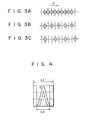
- a new dot-matrix printer has been invented which can print a character in high density as shown in Fig. 2.
- the dots forming this character are arranged at half the pitch of those forming the character of Fig. 1 in the direction F in which the print head moves to print dot characters.
- the printing speed of the dot-matrix printer is usually determined by the maximum response frequency of the print head, i.e., the frequency at which the head moves in direction F. More specifically, the speed is given as f/N [cps], where f is the maximum response frequency of the head and N is the number of dots of each row of the dot matrix. Since the dots are arranged in direction F at half the pitch of those forming the character shown in Fig. 1, the printing speed of the printer is half that of the ordinary dot-matrix printer.
- a dot-matrix printer When a dot-matrix printer prints dots at a far smaller pitch than those forming the character of Fig. 1 as shown in Fig. 3A, its printing speed is given as f/N [cps], where f is the maximum response frequency of the printer. To raise the printing speed, Nmay be decreased. Hence, when the printer prints dots at half the pitch as shown in Fig. 3B, the speed rises to 2f/N [cps]. When the it prints dots at one-third the pitch as illustrated in Fig. 3C, it rises to 3f/N [cps]. Yet the printed characters have better quality since the dots arranged at the pitches (Figs. 3B and 3C) are far smaller than the dots forming the character of Fig. 1.
- the character generated and provided in a dot-matrix printer is a ROM (read-only memory) in most cases.
- the ROM stores the dot patterns corresponding to character codes.
- To print a special character whose dot pattern is not stored in the ROM the ROM must be replaced by a ROM which stores the pattern of the special character. It is troublesome to replace one ROM with another, however.
- a dot-matrix printer has been invented which can register the dot patterns of special characters through an external device.
- This printer is equipped with a character register/generator comprising a RAM (random-access memory) which can store the dot pattern of any character other than those stored in the ROM, which has been input through the external device. The printer can thus print the dot character of any pattern input through the external device.
- the dot-matrix printer described in the preceding paragraph operates in the following manner.
- the external device supplies the printer with a pattern registration command.
- the printer therefore becomes ready to register any dot character pattern.
- a character code, and data showing character pitch Ll (Fig. 4) and character width L2, both shown in Fig. 4 are supplied from the external device to the printer.
- the character width L2 determines the number of bytes representing the dot character pattern to be registered, and the character code determines the address of the RAM in which this pattern is to be registered.
- the dot character pattern is supplied to the RAM and is thus registered therein.
- the pattern To print a dot character, whose pattern has been input through the external device, at a high speed, the pattern must be registered in the form shown in Fig. 3B. However, the more complex the dot pattern is, the more often it is registered in an erroneous form. When the pattern is erroneously registered such that some of its dots are arranged as densely as shown in Fig. 3A, the pins of the print head may be broken during high-speed printing.
- the object of the present invention is to provide a dot-matrix printer whose print head is not damaged even if a dot character is printed at a high speed, whose pattern has been registered through an external device and which is improper for high-speed printing.
- the dot-matrix printer of this invention comprises: buffer memory means for storing printing data containing a dot character pattern input through an external unit and a character code corresponding to the dot character pattern; pattern-checking means for determining whether any two adjacent dots of the pattern which are arranged in the printing direction contact; pattern-correcting means for erasing any adjacent dots if they are found to contact, thereby correcting the dot character pattern; memory means for registering the dot character pattern corrected by the pattern-connecting means or input through the external device at the address corresponding to the character code; and printing means for printing a dot character of the pattern read from the memory means in accordance with the printing data input through the external device.
- the dot character pattern registered in the memory means is checked to see if it is a correct one that can be printed at a high speed without damaging the printing means.
- the pattern is found to be incorrect, it is corrected by the pattern-correcting means.
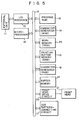
- Fig. 5 is a block diagram of this embodiment, i.e., a dot-matrix printer.
- an I/O interface circuit 10 receives printing data, i.e., a character code, and a dot character pattern to be registered, both supplied from an external unit 11, for example, a host computer.
- the printing data and the code are supplied to a bus 12 from the circuit 10.
- a buffer memory 13 temporarily stores the printing data and the code.
- a CPU 14, i.e., a microprocessor controls the other elements of the printer in accordance with the program stored in a program ROM 15.
- the CPU 14 When the printer is set to the ordinary printing mode, the CPU 14 reads the character code from the buffer memory 13 and causes a ROM 16, i.e., a character generator, to output the dot character pattern corresponding to the character code.
- the ROM 16 stores the dot patterns of ordinary characters.
- a pattern-correcting circuit 17 checks the dot character pattern stored in the buffer memory 13 to determine whether or not the pattern is appropriate for high-speed printing. If the circuit 17 finds this pattern improper for high-speed printing, it corrects the pattern. More specifically, the circuit 17 determines whether or not any two adjacent dots arranged in the printing direction contact, and erases one of these dots if they are in contact, thereby correcting the dot character pattern. The pattern is supplied from the circuit 17 to the buffer memory 13. The dot pattern corrected by the circuit 17 is stored in a RAM 18, i.e., a character register/generator, and is stored at the address corresponding to the character code.
- a RAM 18 i.e., a character register/generator
- the dot character pattern read from the ROM 16 or the RAM 18 is stored in a print buffer 19 (RAM). After storing one line of dot character patterns, the print buffer 19 outputs these patterns, one by one, to a print drive circuit 20. Under the control of the CPU 14 the circuit 20- drives a print head 21 in accordance with the dot character pattern supplied from the print buffer 19.
- a work memory 24 (RAM) is provided to temporarily store the data processed by the CPU 14.
- the circuit 17 has registers 71, 72 and 73 each for storing an 8-bit dot pattern data.
- the register 70 which is made of two chips 74LS174 of Texas Instruments Inc., is used to store nth dot pattern (1 byte) of the character pattern stored in the buffer memory 13.
- the character pattern stored in the buffer memory 13 consists of N 1-byte dot patterns.
- Dot patterns 1, 4, 7...N-1 are arranged in the horizontal direction corresponding to the printing direction F, forming the upper row.
- Dot patterns 2, 5, 8...N-1 are arranged in the same manner, thus forming the middle row.
- Dot patterns 3, 6, 9...N are also arranged horizontally, thus forming the lower row.
- the bits of any dot pattern data (1 byte) stored in the register 70 are inverted and supplied to the first input terminals of AND circuits 73a-73h.
- the register 71 which is made of one chip 74LS373 of Texas Instruments Inc., is used to store the (n+3)th dot pattern read from the buffer memory 13. 'The bits of any dot pattern data stored in the register 71 are supplied to the second input terminals of the AND circuit 73a-73h.
- the 1-byte data formed of the output signals of these AND circuits is input to the register 72 made of chip 74LS374 of Texas Instruments Inc.
- the eight output bits of the register 72 are supplied to the first input terminals of exclusive-OR circuits 74a-74h (hereinafter called EX-OR circuits).
- the bits of the (n+3)th dot pattern stored in the register 71 are supplied to the second input terminals of these EX-OR circuits.
- the output bits of the EX-OR circuits 74a-74h are supplied through inverters 76a-76b to the input terminals of a NAND circuit 75:
- the NAND circuit 75 outputs an error signal E, ⁇ which is supplied to the CPU 14.
- the CPU 14 is model 8085A of Intel Corp.
- the signal E is supplied to the SID (serial input data) terminal of the CPU 14.
- the data stored in the register 72 represents the pattern having its dot arrangement corrected. This data is thus stored in the (n+3)th address of the buffer memory 13.
- the external unit 11 supplies the printer with a pattern registration command.
- the printer therefore becomes ready to register any dot character pattern.
- a dot character pattern to be registerd and printing data containing a character code and data showing the character pitch Ll (Fig. 4) and the character width L2 (Fig. 4) are supplied from the unit 11 to the I/O interface circuit 10.
- the CPU 14 sets the printer to a pattern registration mode so that the dot character pattern defined by the pitches Ll and L2 may be stored in the register RAM 18.
- the dot character pattern and the printing data are temporarily stored in the buffer memory 13.
- the CPU 14 determines the number of bytes representing the dot character pattern, i.e., the size of data to be stored in the RAM 18, in accordance with the character pitch Ll and character width L2, thereby forming a bit pattern (Fig. 7).
- the CPU 14 instructs the pattern-correcting circuit 17 to check whether or not the dots of the input character pattern are arranged in direction F at a pitch appropriate for high-speed printing. That is, the circuit 17 determines whether any two adjacent dots arranged in the printing direction F contact or not. More precisely, the dot pattern 1 stored in the buffer memory 13 is written in the register 70 when a write pulse Rwl is supplied from the CPU 14 to the clock terminal CK of the register 70. The dot pattern 4 in the buffer memory 13 is input to the register 71 when a write pulse RW2 is supplied from the CPU 14 to the clock terminal CK of the register 71. The dot pattern data 4 represents eight dots to the right of those represented by the dot pattern data 1.
- the bits of the dot pattern data 1 are inverted and supplied from the register 70 to the first terminals of the AND circuits 73a-73h.
- the bits of the dot pattern data 4 are supplied to the second input terminals of the AND circuits 73a-73h.
- each of these AND circuit outputs "0" when the bit of the data 1 and the bit of the data 4 at the horizontally aligned position ( F ig. 7) are "1"; it outputs the bits of the data 4 when these two bits have different logical levels.
- any "0" bit shows the absence of a dot and any "1" bit shows the presence of a dot.
- This dot pattern data is stored in the register 72.
- the bits of this data are supplied to the first input terminals of the EX-OR circuits 74a-74h.
- the bits of the dot pattern data 4 stored in the register 71 are supplied to the second input terminals of these EX-OR circuits. Therefore, the NAND circuit 75 outputs an error flag signal E which is at logical "0" level when the dot pattern data in the register 71 is identical with that stored in the register 72 and at logical "1" level when the dot pattern in the register 71 is different from that stored in the register 72.
- This signal E is supplied to the CPU 14. When the signal E is at logical "1," the CPU 14 writes the dot pattern data in the register 72 in the buffer memory 13 in place of the data 4.
- the dot patterns 2 and 5 in the buffer memory 13 are written in the registers 70 and 71 in the same manner as the patterns 1 and 4
- the dot pattern data 2 represents eight dots to the right of those represented by the dot pattern data 5.
- the bits of the data 2 and those of the data 5 are processed in the same way as those representing the dot patterns 1 and 4, so that the dot pattern 5 is corrected or not corrected as the case may be.
- the dot pattern data 3 and the dot pattern data 6 are processed in the same manner. Any other two dot patterns, i.e., the nth and (n+3)th, are processed likewise.
- the dot character pattern stored in the buffer memory 13 is corrected, and no adjacent two dots arranged in direction F contact.
- the dots of the character represented by the data stored in the memory 13 are arranged in the printing direction at the pitch appropriate for high-speed printing.
- the corrected dot character pattern is stored in the register RAM 18. Accordingly, the dot character pattern shown in Fig. 8 in which two dots dl and d2 overlap the adjacent ones is corrected by deleting these dots dl and d2, and the corrected dot character pattern is stored in the register RAM 18.
- the dot character pattern data is supplied from the RAM 18 to the drive circuit 20, whereby the dot character of this pattern is printed at a high speed.
- the operation of the pattern-correcting circuit 17, i.e., the checking and correcting of the character pattern to be registered in the RAM 18, may be performed by the CPU 14 as will be explained with reference to the flow chart of Fig. 9.
- step Sl the CPU 14 loads dot pattern data n from the buffer memory 13 to an accumulator (A). Then, in step S2, the dot pattern data n is inverted and stored in a register (B). The dot pattern data (n+3) is loaded from the memory 13 to the accumulator (A) in step S3. The data (n+3) in the accumulator (A) is stored in a register (C) in step S4. Thereafter, the CPU 14 generates the logical product of the data n stored in the accumulator (A) and the data stored in the register (B) in step S5. That is, the logical product of the data n and the data (n+3) is provided.
- any dot represented by the data (n+3) is deleted if it is at the right of the corresponding dot represented by the data n, whereby the dot pattern data (n+3) is corrected, and the corrected dot pattern data (n+3) is stored in the accumulator (A).
- the CPU 14 compares the corrected data stored in accumulator (A) with the data in the register (C).
- the next dot pattern data is read from the buffer memory 13 in step S7. In this case, it is determined that the dot pattern (n+3) has no dot to the right of the corresponding dot of the pattern n.
- the data in the accumulator (A) is stored in the buffer memory 13, replacing the dot pattern data (n+3), in step S8. In this case, it is determined that the dot pattern (n+3) has at least one dot which is to the right of the corresponding dot of the pattern n.
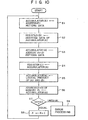
- the checking and correcting of the character pattern to be registered in the RAM 18 may be performed also by the CPU 14 in a different manner, as shown in the flow chart of Fig. 10. That is, before determining in step S7 whether or not at least one dot of the dot pattern (n+3) is positioned right to the corresponding dot of the dot pattern n, the corrected dot pattern (n+3) is stored in the buffer memory 13 in step S6. When the corrected data is different from the data (n+3) stored in the register (C), the CPU 14 performs error processing in step S9; it shows the user of the printer that the dot character pattern he or she has input cannot be registered, by flickering a display made of light-emitting diodes.
- the step S 6 (Fig.
- the user corrects the dot character pattern when he is informed of an error in the pattern, and the corrected pattern is registered in the RAM 18. Also in this case, a dot character pattern which can be printed at a high speed can be registered in the RAM 18.
Abstract
Description
- The present invention relates to a dot-matrix printer of a serial type with a character generator for storing dot character patterns input by operating an external device and for generating the patterns of dot characters to be printed.
- A known dot-matrix printer of a serial type comprises a character generator, a print head-driving circuit and a print head. The printer receives a character code from the external device (usually a host computer). The character generator generates the dot character pattern corresponding to the code. The character patterns are supplied to the print head-driving circuit. This print head driving circuit drives the printing pins of the print head, thereby printing a dot character as shown in Fig. 1.
- Recently it has been increasingly demanded that a dot-matrix printer print dot characters of better quality. To meet this demand, a new dot-matrix printer has been invented which can print a character in high density as shown in Fig. 2. The dots forming this character are arranged at half the pitch of those forming the character of Fig. 1 in the direction F in which the print head moves to print dot characters.
- The printing speed of the dot-matrix printer is usually determined by the maximum response frequency of the print head, i.e., the frequency at which the head moves in direction F. More specifically, the speed is given as f/N [cps], where f is the maximum response frequency of the head and N is the number of dots of each row of the dot matrix. Since the dots are arranged in direction F at half the pitch of those forming the character shown in Fig. 1, the printing speed of the printer is half that of the ordinary dot-matrix printer.
- When a dot-matrix printer prints dots at a far smaller pitch than those forming the character of Fig. 1 as shown in Fig. 3A, its printing speed is given as f/N [cps], where f is the maximum response frequency of the printer. To raise the printing speed, Nmay be decreased. Hence, when the printer prints dots at half the pitch as shown in Fig. 3B, the speed rises to 2f/N [cps]. When the it prints dots at one-third the pitch as illustrated in Fig. 3C, it rises to 3f/N [cps]. Yet the printed characters have better quality since the dots arranged at the pitches (Figs. 3B and 3C) are far smaller than the dots forming the character of Fig. 1.
- The character generated and provided in a dot-matrix printer is a ROM (read-only memory) in most cases. The ROM stores the dot patterns corresponding to character codes. To print a special character whose dot pattern is not stored in the ROM, the ROM must be replaced by a ROM which stores the pattern of the special character. It is troublesome to replace one ROM with another, however. To avoid this trouble, a dot-matrix printer has been invented which can register the dot patterns of special characters through an external device. This printer is equipped with a character register/generator comprising a RAM (random-access memory) which can store the dot pattern of any character other than those stored in the ROM, which has been input through the external device. The printer can thus print the dot character of any pattern input through the external device.
- The dot-matrix printer described in the preceding paragraph operates in the following manner. First, the external device supplies the printer with a pattern registration command. The printer therefore becomes ready to register any dot character pattern. Then, a character code, and data showing character pitch Ll (Fig. 4) and character width L2, both shown in Fig. 4, are supplied from the external device to the printer. The character width L2 determines the number of bytes representing the dot character pattern to be registered, and the character code determines the address of the RAM in which this pattern is to be registered. The dot character pattern is supplied to the RAM and is thus registered therein.
- To print a dot character, whose pattern has been input through the external device, at a high speed, the pattern must be registered in the form shown in Fig. 3B. However, the more complex the dot pattern is, the more often it is registered in an erroneous form. When the pattern is erroneously registered such that some of its dots are arranged as densely as shown in Fig. 3A, the pins of the print head may be broken during high-speed printing.
- Accordingly, the object of the present invention is to provide a dot-matrix printer whose print head is not damaged even if a dot character is printed at a high speed, whose pattern has been registered through an external device and which is improper for high-speed printing.
- The dot-matrix printer of this invention comprises: buffer memory means for storing printing data containing a dot character pattern input through an external unit and a character code corresponding to the dot character pattern; pattern-checking means for determining whether any two adjacent dots of the pattern which are arranged in the printing direction contact; pattern-correcting means for erasing any adjacent dots if they are found to contact, thereby correcting the dot character pattern; memory means for registering the dot character pattern corrected by the pattern-connecting means or input through the external device at the address corresponding to the character code; and printing means for printing a dot character of the pattern read from the memory means in accordance with the printing data input through the external device.
- In the dot-matrix printer of the invention, the dot character pattern registered in the memory means is checked to see if it is a correct one that can be printed at a high speed without damaging the printing means. When the pattern is found to be incorrect, it is corrected by the pattern-correcting means. Hence, even if an erroneous dot character pattern is supplied from the external device, the printer can reliably print the character.
- This invention can be more fully understood from the following detailed description when taken in conjunction with the accompanying drawings, in which:
- Figs. 1 and 2 show the patterns of the dot characters printed by the conventional dot-matrix printers;
- Figs. 3A, 3B and 3C show dot'character patterns, illustrating the operation of a conventional dot-matrix printer;
- Fig. 4 shows the items of printing data which are used in registering the dot pattern of a special character in the character generator of the known dot-matrix printer;
- Fig. 5 is a block diagram of a dot-matrix printer according to the present invention;
- Fig. 6 is a block diagram showing the pattern-correcting circuit of the printer shown in Fig. 5 and the circuits provided near the pattern-correcting circuit;
- Fig. 7 schematically shows the data stored in the print buffer memory of the printer shown in Fig. 5;
- Fig. 8 shows a dot character pattern registered in the print buffer memory; and
- Figs. 9 and 10 are flow charts explaining the operation of the printer shown in Fig. 5.
- One embodiment of the invention will be described with reference to Figs. 5 through Fig. 8. Fig. 5 is a block diagram of this embodiment, i.e., a dot-matrix printer. As shown in this figure, an I/
O interface circuit 10 receives printing data, i.e., a character code, and a dot character pattern to be registered, both supplied from an external unit 11, for example, a host computer. The printing data and the code are supplied to abus 12 from thecircuit 10. Abuffer memory 13 temporarily stores the printing data and the code. ACPU 14, i.e., a microprocessor, controls the other elements of the printer in accordance with the program stored in aprogram ROM 15. When the printer is set to the ordinary printing mode, theCPU 14 reads the character code from thebuffer memory 13 and causes aROM 16, i.e., a character generator, to output the dot character pattern corresponding to the character code. TheROM 16 stores the dot patterns of ordinary characters. - Under the control of the
CPU 14, a pattern-correctingcircuit 17 checks the dot character pattern stored in thebuffer memory 13 to determine whether or not the pattern is appropriate for high-speed printing. If thecircuit 17 finds this pattern improper for high-speed printing, it corrects the pattern. More specifically, thecircuit 17 determines whether or not any two adjacent dots arranged in the printing direction contact, and erases one of these dots if they are in contact, thereby correcting the dot character pattern. The pattern is supplied from thecircuit 17 to thebuffer memory 13. The dot pattern corrected by thecircuit 17 is stored in aRAM 18, i.e., a character register/generator, and is stored at the address corresponding to the character code. - The dot character pattern read from the
ROM 16 or theRAM 18 is stored in a print buffer 19 (RAM). After storing one line of dot character patterns, theprint buffer 19 outputs these patterns, one by one, to aprint drive circuit 20. Under the control of theCPU 14 the circuit 20- drives aprint head 21 in accordance with the dot character pattern supplied from theprint buffer 19. A work memory 24 (RAM) is provided to temporarily store the data processed by theCPU 14. - The pattern-correcting
circuit 17 and the elements connected to it will now be explained with reference to Fig. 6. As shown in this figure, thecircuit 17 hasregisters register 70, which is made of two chips 74LS174 of Texas Instruments Inc., is used to store nth dot pattern (1 byte) of the character pattern stored in thebuffer memory 13. As shown in Fig. 7, the character pattern stored in thebuffer memory 13 consists of N 1-byte dot patterns.Dot patterns Dot patterns Dot patterns - The bits of any dot pattern data (1 byte) stored in the
register 70 are inverted and supplied to the first input terminals of AND circuits 73a-73h. Theregister 71, which is made of one chip 74LS373 of Texas Instruments Inc., is used to store the (n+3)th dot pattern read from thebuffer memory 13. 'The bits of any dot pattern data stored in theregister 71 are supplied to the second input terminals of the AND circuit 73a-73h. The 1-byte data formed of the output signals of these AND circuits is input to theregister 72 made of chip 74LS374 of Texas Instruments Inc. - . The eight output bits of the
register 72 are supplied to the first input terminals of exclusive-OR circuits 74a-74h (hereinafter called EX-OR circuits). The bits of the (n+3)th dot pattern stored in theregister 71 are supplied to the second input terminals of these EX-OR circuits. The output bits of the EX-OR circuits 74a-74h are supplied through inverters 76a-76b to the input terminals of a NAND circuit 75: TheNAND circuit 75 outputs an error signal E, ` which is supplied to theCPU 14. TheCPU 14 ismodel 8085A of Intel Corp. The signal E is supplied to the SID (serial input data) terminal of theCPU 14. The data stored in theregister 72 represents the pattern having its dot arrangement corrected. This data is thus stored in the (n+3)th address of thebuffer memory 13. - The operation of the dot-matrix printer will now be explained. First, the external unit 11 supplies the printer with a pattern registration command. The printer therefore becomes ready to register any dot character pattern. Then, a dot character pattern to be registerd and printing data containing a character code and data showing the character pitch Ll (Fig. 4) and the character width L2 (Fig. 4) are supplied from the unit 11 to the I/
O interface circuit 10. Upon receipt of said command, theCPU 14 sets the printer to a pattern registration mode so that the dot character pattern defined by the pitches Ll and L2 may be stored in theregister RAM 18. The dot character pattern and the printing data are temporarily stored in thebuffer memory 13. TheCPU 14 determines the number of bytes representing the dot character pattern, i.e., the size of data to be stored in theRAM 18, in accordance with the character pitch Ll and character width L2, thereby forming a bit pattern (Fig. 7). - The
CPU 14 instructs the pattern-correctingcircuit 17 to check whether or not the dots of the input character pattern are arranged in direction F at a pitch appropriate for high-speed printing. That is, thecircuit 17 determines whether any two adjacent dots arranged in the printing direction F contact or not. More precisely, thedot pattern 1 stored in thebuffer memory 13 is written in theregister 70 when a write pulse Rwl is supplied from theCPU 14 to the clock terminal CK of theregister 70. Thedot pattern 4 in thebuffer memory 13 is input to theregister 71 when a write pulse RW2 is supplied from theCPU 14 to the clock terminal CK of theregister 71. Thedot pattern data 4 represents eight dots to the right of those represented by thedot pattern data 1. - The bits of the
dot pattern data 1 are inverted and supplied from theregister 70 to the first terminals of the AND circuits 73a-73h. The bits of thedot pattern data 4 are supplied to the second input terminals of the AND circuits 73a-73h. As a result, each of these AND circuit outputs "0" when the bit of thedata 1 and the bit of thedata 4 at the horizontally aligned position (Fig. 7) are "1"; it outputs the bits of thedata 4 when these two bits have different logical levels. Hence, in the dot pattern data formed of the outputs of the AND circuits 73a-73h, any "0" bit shows the absence of a dot and any "1" bit shows the presence of a dot. This dot pattern data is stored in theregister 72. The bits of this data are supplied to the first input terminals of the EX-OR circuits 74a-74h. The bits of thedot pattern data 4 stored in theregister 71 are supplied to the second input terminals of these EX-OR circuits. Therefore, theNAND circuit 75 outputs an error flag signal E which is at logical "0" level when the dot pattern data in theregister 71 is identical with that stored in theregister 72 and at logical "1" level when the dot pattern in theregister 71 is different from that stored in theregister 72. This signal E is supplied to theCPU 14. When the signal E is at logical "1," theCPU 14 writes the dot pattern data in theregister 72 in thebuffer memory 13 in place of thedata 4. - Thereafter, the
dot patterns buffer memory 13 are written in theregisters patterns dot pattern data 2 represents eight dots to the right of those represented by thedot pattern data 5. The bits of thedata 2 and those of thedata 5 are processed in the same way as those representing thedot patterns dot pattern 5 is corrected or not corrected as the case may be. Then, thedot pattern data 3 and thedot pattern data 6 are processed in the same manner. Any other two dot patterns, i.e., the nth and (n+3)th, are processed likewise. - When the last pair of dot patterns (N-3) and N is processed, the dot character pattern stored in the
buffer memory 13 is corrected, and no adjacent two dots arranged in direction F contact. In other words, the dots of the character represented by the data stored in thememory 13 are arranged in the printing direction at the pitch appropriate for high-speed printing. The corrected dot character pattern is stored in theregister RAM 18. Accordingly, the dot character pattern shown in Fig. 8 in which two dots dl and d2 overlap the adjacent ones is corrected by deleting these dots dl and d2, and the corrected dot character pattern is stored in theregister RAM 18. - When the dot-matrix printer is set to the high- speeding printing mode, the dot character pattern data is supplied from the
RAM 18 to thedrive circuit 20, whereby the dot character of this pattern is printed at a high speed. - The operation of the pattern-correcting
circuit 17, i.e., the checking and correcting of the character pattern to be registered in theRAM 18, may be performed by theCPU 14 as will be explained with reference to the flow chart of Fig. 9. - In step Sl, the
CPU 14 loads dot pattern data n from thebuffer memory 13 to an accumulator (A). Then, in step S2, the dot pattern data n is inverted and stored in a register (B). The dot pattern data (n+3) is loaded from thememory 13 to the accumulator (A) in step S3. The data (n+3) in the accumulator (A) is stored in a register (C) in step S4. Thereafter, theCPU 14 generates the logical product of the data n stored in the accumulator (A) and the data stored in the register (B) in step S5. That is, the logical product of the data n and the data (n+3) is provided. More precisely, any dot represented by the data (n+3) is deleted if it is at the right of the corresponding dot represented by the data n, whereby the dot pattern data (n+3) is corrected, and the corrected dot pattern data (n+3) is stored in the accumulator (A). Instep 6, theCPU 14 compares the corrected data stored in accumulator (A) with the data in the register (C). - If the data in the accumulator (A) is identical with the data (n+3) stored in the register (C), the next dot pattern data is read from the
buffer memory 13 in step S7. In this case, it is determined that the dot pattern (n+3) has no dot to the right of the corresponding dot of the pattern n. - If the corrected data is different from the data (n+3) stored in the register (C), the data in the accumulator (A) is stored in the
buffer memory 13, replacing the dot pattern data (n+3), in step S8. In this case, it is determined that the dot pattern (n+3) has at least one dot which is to the right of the corresponding dot of the pattern n. - The checking and correcting of the character pattern to be registered in the
RAM 18 may be performed also by theCPU 14 in a different manner, as shown in the flow chart of Fig. 10. That is, before determining in step S7 whether or not at least one dot of the dot pattern (n+3) is positioned right to the corresponding dot of the dot pattern n, the corrected dot pattern (n+3) is stored in thebuffer memory 13 in step S6. When the corrected data is different from the data (n+3) stored in the register (C), theCPU 14 performs error processing in step S9; it shows the user of the printer that the dot character pattern he or she has input cannot be registered, by flickering a display made of light-emitting diodes. The step S6 (Fig. 10) may be omitted. If this is the case, the user corrects the dot character pattern when he is informed of an error in the pattern, and the corrected pattern is registered in theRAM 18. Also in this case, a dot character pattern which can be printed at a high speed can be registered in theRAM 18.
Claims (6)
Applications Claiming Priority (2)
| Application Number | Priority Date | Filing Date | Title |
|---|---|---|---|
| JP225739/83 | 1983-11-30 | ||
| JP58225739A JPS60116464A (en) | 1983-11-30 | 1983-11-30 | Printer |
Publications (3)
| Publication Number | Publication Date |
|---|---|
| EP0144016A2 true EP0144016A2 (en) | 1985-06-12 |
| EP0144016A3 EP0144016A3 (en) | 1987-11-11 |
| EP0144016B1 EP0144016B1 (en) | 1990-09-05 |
Family
ID=16834073
Family Applications (1)
| Application Number | Title | Priority Date | Filing Date |
|---|---|---|---|
| EP84113650A Expired EP0144016B1 (en) | 1983-11-30 | 1984-11-12 | Dot-matrix printer |
Country Status (6)
| Country | Link |
|---|---|
| US (1) | US4629342A (en) |
| EP (1) | EP0144016B1 (en) |
| JP (1) | JPS60116464A (en) |
| AU (1) | AU551707B2 (en) |
| CA (1) | CA1217567A (en) |
| DE (1) | DE3483136D1 (en) |
Cited By (8)
| Publication number | Priority date | Publication date | Assignee | Title |
|---|---|---|---|---|
| EP0207788A2 (en) * | 1985-07-03 | 1987-01-07 | Lexmark International, Inc. | Apparatus and method for displaying dot matrix characters in enhanced form |
| FR2622838A1 (en) * | 1987-11-05 | 1989-05-12 | Canon Kk | INKJET RECORDING METHOD |
| EP0331033A2 (en) * | 1988-02-29 | 1989-09-06 | Oki Electric Industry Company, Limited | Printing system for dot-matrix printer |
| EP0359581A2 (en) * | 1988-09-16 | 1990-03-21 | Ncr Corporation | Control system for dot matrix printer |
| US4953102A (en) * | 1985-03-30 | 1990-08-28 | Mita Industrial Co., Ltd. | Method for producing character patterns |
| EP0513989A2 (en) * | 1991-04-17 | 1992-11-19 | Hewlett-Packard Company | Raster imaging device speed-resolution product multiplying method and resulting pixel image data structure |
| US5237344A (en) * | 1987-11-05 | 1993-08-17 | Canon Kabushiki Kaisha | Ink jet recording apparatus and method with dot thinning |
| EP0576261A2 (en) * | 1992-06-23 | 1993-12-29 | Tektronix, Inc. | Improved phase change ink printing on light-transmissive substrates |
Families Citing this family (17)
| Publication number | Priority date | Publication date | Assignee | Title |
|---|---|---|---|---|
| US4613945A (en) * | 1984-05-07 | 1986-09-23 | Pitney Bowes Inc. | Method and apparatus for creating fonts for an electronic character generator |
| JPH0719192B2 (en) * | 1985-02-15 | 1995-03-06 | シチズン時計株式会社 | How to use memory in printer |
| JPS6490765A (en) * | 1987-10-02 | 1989-04-07 | Fujitsu Ltd | Printing control method |
| JPH0832469B2 (en) * | 1988-01-29 | 1996-03-29 | 富士通株式会社 | Horizontal expansion method of bitmap font |
| EP0372810A3 (en) * | 1988-12-02 | 1991-07-10 | Spectra-Physics, Inc. | Inkjet printers |
| US5247609A (en) * | 1988-12-08 | 1993-09-21 | Thermo Separation Products (California) Inc. | Line density control for plotters |
| US5016195A (en) * | 1989-03-03 | 1991-05-14 | Da Vinci Graphics, Inc. | High quality plotting technique for raster printing devices |
| JPH02243373A (en) * | 1989-03-17 | 1990-09-27 | Hitachi Ltd | Print misregistration correcting method and printer for practicing same method |
| DE69122915T2 (en) * | 1990-07-13 | 1997-02-27 | Adobe Systems Inc | Process for the preparation of matrix characters with small dimensions using connected rows of pixels |
| JPH04195639A (en) * | 1990-11-28 | 1992-07-15 | Teijin Seiki Co Ltd | Multiprocessor system and control method of its output |
| US5588094A (en) * | 1994-01-03 | 1996-12-24 | Tektronix, Inc. | Post-processing bit-map decimation compensation method for printing high quality images |
| US5677714A (en) * | 1995-01-03 | 1997-10-14 | Xerox Corporation | Neighbor insentive pixel deletion method for printing high resolution image |
| US5742300A (en) * | 1995-01-03 | 1998-04-21 | Xerox Corporation | Resolution enhancement and thinning method for printing pixel images |
| US5767870A (en) * | 1995-01-03 | 1998-06-16 | Xerox Corporation | Edge insensitive pixel deletion method for printing high resolution image |
| US5719601A (en) * | 1995-01-03 | 1998-02-17 | Xerox Corporation | Intentional underthinning of 600×300 image data when printing in multi-pass mode |
| DE19724066B4 (en) * | 1997-06-07 | 2007-04-19 | Man Roland Druckmaschinen Ag | Method for correcting geometry errors when transferring information to a substrate |
| JP3954246B2 (en) * | 1999-08-11 | 2007-08-08 | 独立行政法人科学技術振興機構 | Document processing method, recording medium storing document processing program, and document processing apparatus |
Citations (2)
| Publication number | Priority date | Publication date | Assignee | Title |
|---|---|---|---|---|
| DE2515557A1 (en) * | 1975-04-09 | 1976-10-21 | Mannesmann Ag | Matrix printer with variable letter width - controlling use of gaps between matrix points varies width |
| US4347518A (en) * | 1979-09-04 | 1982-08-31 | Gould Inc. | Thermal array protection apparatus |
Family Cites Families (4)
| Publication number | Priority date | Publication date | Assignee | Title |
|---|---|---|---|---|
| DE2635398C2 (en) * | 1976-08-06 | 1982-10-14 | Philips Patentverwaltung Gmbh, 2000 Hamburg | Method and arrangement for controlling the printing magnets of a matrix printer |
| US4291992A (en) * | 1979-05-22 | 1981-09-29 | R. C. Sanders Technology Systems, Inc. | Printer pin control circuitry |
| US4339208A (en) * | 1980-09-25 | 1982-07-13 | Ncr Corporation | Optical sensing of wire matrix printers |
| JPS58145463A (en) * | 1982-02-22 | 1983-08-30 | Toshiba Corp | Printing controller |
-
1983
- 1983-11-30 JP JP58225739A patent/JPS60116464A/en active Pending
-
1984
- 1984-11-12 AU AU35334/84A patent/AU551707B2/en not_active Ceased
- 1984-11-12 EP EP84113650A patent/EP0144016B1/en not_active Expired
- 1984-11-12 DE DE8484113650T patent/DE3483136D1/en not_active Expired - Lifetime
- 1984-11-16 US US06/672,493 patent/US4629342A/en not_active Expired - Fee Related
- 1984-11-28 CA CA000468815A patent/CA1217567A/en not_active Expired
Patent Citations (2)
| Publication number | Priority date | Publication date | Assignee | Title |
|---|---|---|---|---|
| DE2515557A1 (en) * | 1975-04-09 | 1976-10-21 | Mannesmann Ag | Matrix printer with variable letter width - controlling use of gaps between matrix points varies width |
| US4347518A (en) * | 1979-09-04 | 1982-08-31 | Gould Inc. | Thermal array protection apparatus |
Cited By (17)
| Publication number | Priority date | Publication date | Assignee | Title |
|---|---|---|---|---|
| US4953102A (en) * | 1985-03-30 | 1990-08-28 | Mita Industrial Co., Ltd. | Method for producing character patterns |
| EP0207788A3 (en) * | 1985-07-03 | 1989-06-14 | International Business Machines Corporation | Apparatus and method for displaying dot matrix characters in enhanced form |
| EP0207788A2 (en) * | 1985-07-03 | 1987-01-07 | Lexmark International, Inc. | Apparatus and method for displaying dot matrix characters in enhanced form |
| FR2622838A1 (en) * | 1987-11-05 | 1989-05-12 | Canon Kk | INKJET RECORDING METHOD |
| EP0317140A2 (en) * | 1987-11-05 | 1989-05-24 | Canon Kabushiki Kaisha | Ink jet recording apparatus |
| US5237344A (en) * | 1987-11-05 | 1993-08-17 | Canon Kabushiki Kaisha | Ink jet recording apparatus and method with dot thinning |
| EP0317140A3 (en) * | 1987-11-05 | 1989-11-15 | Canon Kabushiki Kaisha | Ink jet recording method |
| US5155503A (en) * | 1987-11-05 | 1992-10-13 | Canon Kabushiki Kaisha | Ink jet recording apparatus with detection of environmental condition used to control dot thinning rate |
| EP0331033A2 (en) * | 1988-02-29 | 1989-09-06 | Oki Electric Industry Company, Limited | Printing system for dot-matrix printer |
| EP0331033A3 (en) * | 1988-02-29 | 1989-10-18 | Oki Electric Industry Company, Limited | Printing system for dot-matrix printer |
| EP0359581A3 (en) * | 1988-09-16 | 1992-03-04 | Ncr Corporation | Control system for dot matrix printer |
| EP0359581A2 (en) * | 1988-09-16 | 1990-03-21 | Ncr Corporation | Control system for dot matrix printer |
| EP0513989A2 (en) * | 1991-04-17 | 1992-11-19 | Hewlett-Packard Company | Raster imaging device speed-resolution product multiplying method and resulting pixel image data structure |
| EP0513989A3 (en) * | 1991-04-17 | 1993-07-14 | Hewlett-Packard Company | Raster imaging device speed-resolution product multiplying method and resulting pixel image data structure |
| US5270728A (en) * | 1991-04-17 | 1993-12-14 | Hewlett-Packard Company | Raster imaging device speed-resolution product multiplying method and resulting pixel image data structure |
| EP0576261A2 (en) * | 1992-06-23 | 1993-12-29 | Tektronix, Inc. | Improved phase change ink printing on light-transmissive substrates |
| EP0576261A3 (en) * | 1992-06-23 | 1994-06-01 | Tektronix Inc | Improved phase change ink printing on light-transmissive substrates |
Also Published As
| Publication number | Publication date |
|---|---|
| US4629342A (en) | 1986-12-16 |
| EP0144016A3 (en) | 1987-11-11 |
| AU3533484A (en) | 1985-06-06 |
| AU551707B2 (en) | 1986-05-08 |
| EP0144016B1 (en) | 1990-09-05 |
| CA1217567A (en) | 1987-02-03 |
| JPS60116464A (en) | 1985-06-22 |
| DE3483136D1 (en) | 1990-10-11 |
Similar Documents
| Publication | Publication Date | Title |
|---|---|---|
| US4629342A (en) | Dot-matrix printer with pattern checking and pattern correcting means | |
| EP0081653B1 (en) | Method of recording and reading optimum density bar code | |
| US3999168A (en) | Intermixed pitches in a buffered printer | |
| US4031519A (en) | Printer | |
| US4660999A (en) | Dot-matrix printer with font cartridge unit | |
| EP0217043A1 (en) | Thermal print head heating circuit fault detection device | |
| US4007442A (en) | Intermixed line heights and blank line formation in a buffered printer | |
| KR930000180B1 (en) | Thermal printer for a portable data terminal | |
| EP0211640B1 (en) | Thermal printing system | |
| US6449665B1 (en) | Means for reducing direct memory access | |
| EP0317996A2 (en) | Printer | |
| EP0145961A1 (en) | Printing apparatus | |
| JPS60129266A (en) | Line printing system for dot printer | |
| US4621343A (en) | Circuit arrangement for detecting error in print control apparatus | |
| JPH01249366A (en) | Thermal recording apparatus | |
| JPS5942357B2 (en) | Character pattern error check method | |
| KR910009064B1 (en) | Method for compensating character size of printer | |
| JPS6038167A (en) | Character or figure pattern generating circuit device | |
| JPH0211357A (en) | Printing apparatus | |
| EP0072708A2 (en) | Printer | |
| JP2566652B2 (en) | Dot line recorder | |
| JP3055738B2 (en) | Dot matrix pattern printing method and apparatus | |
| JP2907143B2 (en) | LED printer device | |
| JPH0371028B2 (en) | ||
| EP0114948A1 (en) | Control system for a line printer having an endless type carrier |
Legal Events
| Date | Code | Title | Description |
|---|---|---|---|
| PUAI | Public reference made under article 153(3) epc to a published international application that has entered the european phase |
Free format text: ORIGINAL CODE: 0009012 |
|
| 17P | Request for examination filed |
Effective date: 19841207 |
|
| AK | Designated contracting states |
Designated state(s): DE FR GB SE |
|
| PUAL | Search report despatched |
Free format text: ORIGINAL CODE: 0009013 |
|
| AK | Designated contracting states |
Kind code of ref document: A3 Designated state(s): DE FR GB SE |
|
| 17Q | First examination report despatched |
Effective date: 19880922 |
|
| GRAA | (expected) grant |
Free format text: ORIGINAL CODE: 0009210 |
|
| AK | Designated contracting states |
Kind code of ref document: B1 Designated state(s): DE FR GB SE |
|
| REF | Corresponds to: |
Ref document number: 3483136 Country of ref document: DE Date of ref document: 19901011 |
|
| ET | Fr: translation filed | ||
| PLBE | No opposition filed within time limit |
Free format text: ORIGINAL CODE: 0009261 |
|
| STAA | Information on the status of an ep patent application or granted ep patent |
Free format text: STATUS: NO OPPOSITION FILED WITHIN TIME LIMIT |
|
| 26N | No opposition filed | ||
| EAL | Se: european patent in force in sweden |
Ref document number: 84113650.0 |
|
| PGFP | Annual fee paid to national office [announced via postgrant information from national office to epo] |
Ref country code: FR Payment date: 19951109 Year of fee payment: 12 |
|
| PGFP | Annual fee paid to national office [announced via postgrant information from national office to epo] |
Ref country code: DE Payment date: 19951113 Year of fee payment: 12 |
|
| PGFP | Annual fee paid to national office [announced via postgrant information from national office to epo] |
Ref country code: SE Payment date: 19951116 Year of fee payment: 12 |
|
| PGFP | Annual fee paid to national office [announced via postgrant information from national office to epo] |
Ref country code: GB Payment date: 19961104 Year of fee payment: 13 |
|
| PG25 | Lapsed in a contracting state [announced via postgrant information from national office to epo] |
Ref country code: SE Effective date: 19961113 |
|
| PG25 | Lapsed in a contracting state [announced via postgrant information from national office to epo] |
Ref country code: FR Effective date: 19970731 |
|
| PG25 | Lapsed in a contracting state [announced via postgrant information from national office to epo] |
Ref country code: DE Effective date: 19970801 |
|
| EUG | Se: european patent has lapsed |
Ref document number: 84113650.0 |
|
| REG | Reference to a national code |
Ref country code: FR Ref legal event code: ST |
|
| PG25 | Lapsed in a contracting state [announced via postgrant information from national office to epo] |
Ref country code: GB Free format text: LAPSE BECAUSE OF NON-PAYMENT OF DUE FEES Effective date: 19971112 |
|
| GBPC | Gb: european patent ceased through non-payment of renewal fee |
Effective date: 19971112 |