EP0146032B1 - Method and apparatus for the conversion of a polyphase voltage system - Google Patents
Method and apparatus for the conversion of a polyphase voltage system Download PDFInfo
- Publication number
- EP0146032B1 EP0146032B1 EP84114357A EP84114357A EP0146032B1 EP 0146032 B1 EP0146032 B1 EP 0146032B1 EP 84114357 A EP84114357 A EP 84114357A EP 84114357 A EP84114357 A EP 84114357A EP 0146032 B1 EP0146032 B1 EP 0146032B1
- Authority
- EP
- European Patent Office
- Prior art keywords
- phase
- input
- output
- frequency
- amplitude
- Prior art date
- Legal status (The legal status is an assumption and is not a legal conclusion. Google has not performed a legal analysis and makes no representation as to the accuracy of the status listed.)
- Expired
Links
Images

Classifications
-
- H—ELECTRICITY
- H02—GENERATION; CONVERSION OR DISTRIBUTION OF ELECTRIC POWER
- H02M—APPARATUS FOR CONVERSION BETWEEN AC AND AC, BETWEEN AC AND DC, OR BETWEEN DC AND DC, AND FOR USE WITH MAINS OR SIMILAR POWER SUPPLY SYSTEMS; CONVERSION OF DC OR AC INPUT POWER INTO SURGE OUTPUT POWER; CONTROL OR REGULATION THEREOF
- H02M5/00—Conversion of ac power input into ac power output, e.g. for change of voltage, for change of frequency, for change of number of phases
- H02M5/02—Conversion of ac power input into ac power output, e.g. for change of voltage, for change of frequency, for change of number of phases without intermediate conversion into dc
- H02M5/04—Conversion of ac power input into ac power output, e.g. for change of voltage, for change of frequency, for change of number of phases without intermediate conversion into dc by static converters
- H02M5/22—Conversion of ac power input into ac power output, e.g. for change of voltage, for change of frequency, for change of number of phases without intermediate conversion into dc by static converters using discharge tubes with control electrode or semiconductor devices with control electrode
- H02M5/25—Conversion of ac power input into ac power output, e.g. for change of voltage, for change of frequency, for change of number of phases without intermediate conversion into dc by static converters using discharge tubes with control electrode or semiconductor devices with control electrode using devices of a thyratron or thyristor type requiring extinguishing means
- H02M5/27—Conversion of ac power input into ac power output, e.g. for change of voltage, for change of frequency, for change of number of phases without intermediate conversion into dc by static converters using discharge tubes with control electrode or semiconductor devices with control electrode using devices of a thyratron or thyristor type requiring extinguishing means for conversion of frequency
- H02M5/271—Conversion of ac power input into ac power output, e.g. for change of voltage, for change of frequency, for change of number of phases without intermediate conversion into dc by static converters using discharge tubes with control electrode or semiconductor devices with control electrode using devices of a thyratron or thyristor type requiring extinguishing means for conversion of frequency from a three phase input voltage
Definitions
- the present invention relates to a direct AC-AC frequency converter, i.e. a converter of electric energy able to convert a polyphase AC input supply into an equivalent polyphase AC (or possibly DC) output system with frequency, amplitude and phase independently controllable, without any intermediate conversion step through a DC system.
- a direct AC-AC frequency converter i.e. a converter of electric energy able to convert a polyphase AC input supply into an equivalent polyphase AC (or possibly DC) output system with frequency, amplitude and phase independently controllable, without any intermediate conversion step through a DC system.
- a power supply with a frequency and an amplitude that are different from those available such as the variable speed drive of induction or synchronous motors, by adjusting simultaneously both the frequency and the amplitude of the supply system, the constant frequency, variable speed generators (VSCF), whereby the variable frequency energy produced by the prime mover (typically an airplane turbine) is converted to constant frequency before use, etc.
- VSCF constant frequency, variable speed generators
- the use of higher than line, controlled frequency allows important advantages in the design of almost all electric machines.
- frequency converters are known, which, for different reasons, do not fully provide the desirable features listed above.
- existing frequency converters can be grouped into two categories: AC-DC-AC converters and direct converters.
- the converters of the former type consist of two stages; in the first, the AC input is converted into an intermediate DC bus, which is in turn converted by the second stage into an output AC system with the desired properties.
- the most common drawbacks of this type of machines are the generally unidirectional energy flow, the need for large reactive elements in the intermediate filter, and non-sinusoidal waveforms.
- Direct converters synthetize the AC output directly out of t AC input without any intermediate stage. They consist of a number of switches connecting the input phases with the output phases in different combinations and of various types of filters.
- the best known converter of this type are the cycloconverter, the UFC (Universal Frequency Changer) and SEC (Slow Frequency Changer) and the HSFC (High Speed Frequency Changer) disclosed by the first inventor in GB-A-2 048 588.
- the output waveform is a piece-wise approximation of the desired sinusoid obtained by sampling the input phases once per input cycle, by means of a matrix of switches, and according to different control methods. Consequently, the quality of the output waveform can only be improved by increasing the number of the input phases, and of the switches, with obvious cost penalties.
- the HFSC synthetizes the output waveforms by sequentially connecting all the input phases to any given output phase, at frequency substantially higher than both the input and the set output frequency, and by modulating the sampling time of each input phase proportionally to a suitable combination of two sinusoids, where such sinusoids have a frequency which is proportional to the sum of and to the difference between the set output frequency and the input frequency. Therefore, the output waveforms, and symmetrically the input waveforms, consist of a sinusoidal low frequency component, as measured with respect to the input neutral conductor, whose amplitude, frequency and phase are independently controllable, and of a cluster of high frequency harmonics, centered around and above the sampling frequency, and therefore easy to be filtered if necessary.
- the input current is also sinusoidal and the relevent phase displacement is controllable but subject to the limitation that the absolute value of the input phase angle is less than or equal to the output phase angle.
- the HSFC allows for a continuous and independent control of frequency, amplitude and phase; however, the output amplitude is intrinsecally limited to 0.5 times the input amplitude.
- the switch matrix must be designed to withstand the full input voltage, this feature implies a non optimal use of the power semiconductors in the matrix.
- the ratio between the trigonometric tangents of the input and output phase angles is limited to be no greater than 1 in module, which prevents the use of the converter in a number of applications related to reactive power compensation such as static VARs.
- a further object of the invention is to realize a method for converting a polyphase balanced system into another one, more particularly a three phase system into a three phase system having different amplitude, frequency and/or phase angle.
- the invention consists of a method for directly converting a three phase input voltage system, balanced and sinusoidal, having input amplitude v,, frequency w i /2 ⁇ and phase angle s,, into a three phase output voltage system, also balanced and sinusoidal, and having output voltage v o , frequency wo/2n and phase angle so wherein at least one of the latter quantities is different from the former, and each output waveform is obtained by sequentially sampling all the input phases and said sampling is carried out through nine modulation coefficients m k , h (t) expressing the ratios between the time that the input phase h is connected to the output phase k and the overall sampling period, whereby said modulation coefficients contain components at the frequencies 3w o ⁇ w, with the same amplitude; at the frequencies 2w, and 4w, the amplitudes of which are in a constant ratio of 7:1 and of opposite sign, and at frequencies w o ⁇ w, with the ratio of their amplitude being a function of tg(s l
- the invention further consists in a method as above indicated in which the modulation coefficients are the entries of the following matrix: where: with:
- the invention consists in a direct AC converter including three input phase conductors and a neutral conductor for a balanced three phase AC input voltage system, three output phase conductors and a neutral conductor for a three phase AC output voltage system having at least one characteristic such as frequency, amplitude, phase angle or phase displacement which is different from that of the input voltage system, the input and output neutral conductors being unconnected between them, the converter building up the output voltage through a 3x3 matrix of bidirectional electronic controlled switches subsequently connecting each output phase conductor with each input phase conductor, characterized by the fact that said switches are operated in accordance with the method.
- Such frequency converter consists of a number of bidirectional electronic switches, which connect each input conductor with each output conductor, and which are operated at a substantially higher frequency (from 5 to 20 times) than both the input and the set output frequency, driven by a logic control circuit such that for each output phase, at any given time, one and only one switch is closed.
- the control circuit drives the switches with variable duty cycle as will be detailed later on.
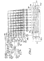
- the direct converter shown in Figure 1 comprises two main portions, more precisely a plurality of controlled electronic switches SW1...SWS arranged to form a switch matrix MU, and a control circuit supplying the necessary control or drive signals to the switches, illustrated in the remaining portion of the drawing.
- the converter is connected between a three phase input voltage system LI through a filter I, and a three phase output voltage system LU through a filter U.
- the matrix MU consists of nine switches which connect any given input conductor with all output conductors. More generally, for polyphase systems with n input lines and m output lines, the switch matrix consists of nxm switches. Such switches must be adequate to withstand the maximum supply voltage as well as the maximum load current.
- the corresponding output phase conductor can be connected with all the input conductors through the switches SW1, SW2, SW3 out of the SW1...SW9 switches of the matrix.
- Such switches are cyclically operated, i.e. closed, at a frequency f c , where f c is substantially higher (e.g. 10 times) than the highest of both the input and output frequencies, and in such a way that at any time one and only one of SW1, SW2, SW3 is closed.
- the cycle time 1/f o is very short, the three input voltages do not vary appreciably during the switching cycle.
- m 11 (t), m 12 (t), m 13 (t) be the ratios between the time during which the output conductor (1) is connected to the corresponding input conductor (1, or 3) and the overall switching cycle T c , i.e. the duty cycles of SW1, SW2, SW3 within the cycle T.
- V 11 , V 12 , V, 3 are the three input voltages during T c , as measured with respect to the neutral input conductor N, then the output waveform consists of three samples of the input voltages and will have an average amplitude, within T c , approximately equal to:
- the output waveforms amplitudes as referenced to the input neutral conductor are the following: p being a parameter that will be defined later and comprised between zero and one.
- phase to phase output voltages are: i.e. they are sinusoidal and with the correct phase relationships.
- the waveforms represented in (1) allow for maximizing the output phase to phase voltages (2) without exceeding the fundamental limitation of this type of converter, with respect to the range of the input voltages.
- any of the output voltages (e.g. V oi ) as measured between the corresponding phase conductor and the input neutral conductor, comprises the usual component at the desired output frequency (v o cos(w o (t)) with the proper phase angle, and a common term given by
- This term is formed as a linear combination of two sinusoidal waveforms, the first one at a frequency that is three times the output frequency, and the second one at a frequency that is three times the input frequency.
- the common term will be a linear combination of two sinusoidal waveforms, one having a frequency which is m times the output frequency, and the other having a frequency which is n times the input frequency.
- the converter of the present invention is therefore capable of synthesizing waveforms of the type represented in (1).
- Such waveforms are synthetized as follows:
- each of the element mk,h(t) representing the duty cycle of the corresponding switch SW is formed by a linear combination of six sinusoidal terms (as given by relationship (3)).
- Relationship (12) represents anyone of the three voltages of relationship (1) when using the compact notation given by (3).
- Relationship (13) represents, with the same notation, the input current of phase h.
- the ratio S between the trigonometrical tangents of the input and output phase displacements can be greater than 1 since this does not lead to values of the duty cycle, as expressed by mk,h(t), that are either negative or higher than 1. Therefore the controllable range of the input-output phase displacement is greatly enlarged.
- control circuit capable of generating drive signals according to (6)...(11) is now described with reference to Figure 1.
- Said control circuit converts the input control variables such as desired output frequency, amplitude and ratio between tangents of input and output phase displacement, into the appropriate drive signals for the power switches in MU.
- the control circuit in its simplest form has four input control lines and nine output control lines.
- the input control signals are the desired ratio between the output and input voltages v o /v i , the desired ratio tg(s,)/tg(s o ), the desired output frequency and the actual input frequency;
- the output control signals are the drive pulses for the matrix MU.
- said control circuit can be either an analog one ( Figure 1) or a digital one ( Figures 4A, 4B, 5A, 5B).
- the output frequency is set through the circuit Q1 comprising a voltage source and a potentiometer.
- a voltage controlled oscillator VC converts said voltage into an AC voltage having the frequency equal to the desired one (w o ) and an AC voltage having a frequency which is three times the former (3w o ).
- the input frequency is sensed on LI, shaped and squared by filter F. With this signal, the phase locked loop PL7 generates two synchronous AC voltages with frequency two and four times the input frequency (2w, and 4w,).
- phase locked loops PL1...PL6 are three phase, sinusoidal with controllable amplitude, and can be synchronized on the sum or the difference of two input frequencies.
- the so obtained signal proportional to S is fed to a comparator C1 and a rectifier R1.
- the output from R1 is therefore proportional to
- circuit Q4 comprising a voltage source and a potentiometer.
- the network comprising X1 and A1, a multiplier and an amplifier respectively, result in a signal proportional to a according to (8), while adder/amplifier A2 together with multiplier X2 provide a signal proportional to p according to (9).
- This signal is fed to amplifiers A5, A6 to control the amplitudes of PL3, PL4, while its absolute value, obtained by rectifier R2, is used to control the amplitude_of PL5 and PL6 through amplifiers A7, A8.
- the voltage gains of A5...A8 are proportional to
- signal a and the value zero are fed to multiplexer M in direct and reverse sequence, M being controlled by C1 so that signals a 1 , a 2 according to (10) are available on the multiplexed outputs of M.
- Such outputs are fed to adders A3, A4 together with signal p and the resulting outputs control PL1, PL2 amplitudes according to (6).
- the eighteen signals provided by PL1...PL6 are proportional to the sinusoidal components which form the duty cycle coefficients m k , h (t) according to (6)...(11). These signals are combined, in the correct order, by adders S1...S9 which output signals, proportional to mk,h(t) as given by (11), also providing the fixed offset required by (6). Such outputs are converted into drive pulses by programmable timers T1...T9 whose output pulse durations are proportional to the amplitude fed at the programming input.
- the timers are connected in rings of three units, where each group is connected to a single output line, in such a way that the end of each timer cycle would trigger the start of the next timer.
- Timer outputs are decoupled and amplified by driver circuits D1...D9 which drive the power switches SW1...SW9 in the power switch matrix.
- the converter can be completed by optional input and output filters I and U, capacitive and inductive respectively, which may be required with high impedance supply or with non-inductive loads.
- a digital processor is used to compute and evaluate the numerical values of matrix (11) at regular intervals, much shorter anyway than the duration of both input and output cycles. For example, in an application where both input and output frequencies are below 100 Hz, the matrix M(t) can be evaluated once every millisecond.
- the program of the processor consists of an initialization routine ( Figure 4A) which upon processor start up or on interrupt whenever the control parameters are changed, inputs the values of w,, w o , v,, v o , S and evaluates constants a,, a 2 , p according to (8) (9) (10).
- Two subroutines ( Figures 4B, 5A) can be defined to simplify the main program. The first one ( Figure 4B) generates the function ZO(y)(t) as defined by (3) whereas the second one ( Figure 5A) generates function m(x 1 ,...,x 6 ) as defined by (6). After the execution of the control is returned to the main program.
- the processor timer updates the time register t, and evaluates M(t) with the mentioned subroutines.
- the nine numbers thus obtained are then fed to digital to time duration converters or down counters, which drive in sequence, through driver circuits, the nine power switches in MU as described before.
- the power switches which form MU can be realized in many already known ways, for example as described in the cited U.S. Patent, or with newer components such as bidirectional power MOSFETs or COMFETs.
Description
- The present invention relates to a direct AC-AC frequency converter, i.e. a converter of electric energy able to convert a polyphase AC input supply into an equivalent polyphase AC (or possibly DC) output system with frequency, amplitude and phase independently controllable, without any intermediate conversion step through a DC system.
- Many applications require a power supply with a frequency and an amplitude that are different from those available, such as the variable speed drive of induction or synchronous motors, by adjusting simultaneously both the frequency and the amplitude of the supply system, the constant frequency, variable speed generators (VSCF), whereby the variable frequency energy produced by the prime mover (typically an airplane turbine) is converted to constant frequency before use, etc. As a general rule, the use of higher than line, controlled frequency allows important advantages in the design of almost all electric machines.
- By adjusting the phase angle of the energy flowing through the converter, an important optimization of the load on the supply network is also possible.
- The most desirable features of a frequency converter can be listed as follows:
- 1) Continuous control of output frequency and amplitude;
- 2) Sinusoidal input and output waveforms. In particular, subharmonics or harmonics near to the selected frequency must be minimized. Actually, any inductive load, having a low impedance at low frequency, acts as a subharmonic amplifier and would distort the current waveforms considerably.
- 3) Bidirectional energy flow (to allow for generators, braking motors, etc.);
- 4) Minimal use of reactive and dissipative elements, whose integration and scaling is impossible and whose impact on the converter cost is therefore destined to be predominant;
- 5) Maximum utilization of semiconductor technology;
- 6) Control of the input phase angle independently from the output phase angle.
- Several types of frequency converters are known, which, for different reasons, do not fully provide the desirable features listed above. In general, existing frequency converters can be grouped into two categories: AC-DC-AC converters and direct converters.
- The converters of the former type consist of two stages; in the first, the AC input is converted into an intermediate DC bus, which is in turn converted by the second stage into an output AC system with the desired properties. Among the most common drawbacks of this type of machines are the generally unidirectional energy flow, the need for large reactive elements in the intermediate filter, and non-sinusoidal waveforms.
- Direct converters, on the other hand, synthetize the AC output directly out of t AC input without any intermediate stage. They consist of a number of switches connecting the input phases with the output phases in different combinations and of various types of filters. The best known converter of this type are the cycloconverter, the UFC (Universal Frequency Changer) and SEC (Slow Frequency Changer) and the HSFC (High Speed Frequency Changer) disclosed by the first inventor in GB-A-2 048 588.
- More in detail in the first three converter quoted the output waveform is a piece-wise approximation of the desired sinusoid obtained by sampling the input phases once per input cycle, by means of a matrix of switches, and according to different control methods. Consequently, the quality of the output waveform can only be improved by increasing the number of the input phases, and of the switches, with obvious cost penalties.
- On the other hand, the HFSC synthetizes the output waveforms by sequentially connecting all the input phases to any given output phase, at frequency substantially higher than both the input and the set output frequency, and by modulating the sampling time of each input phase proportionally to a suitable combination of two sinusoids, where such sinusoids have a frequency which is proportional to the sum of and to the difference between the set output frequency and the input frequency. Therefore, the output waveforms, and symmetrically the input waveforms, consist of a sinusoidal low frequency component, as measured with respect to the input neutral conductor, whose amplitude, frequency and phase are independently controllable, and of a cluster of high frequency harmonics, centered around and above the sampling frequency, and therefore easy to be filtered if necessary.
- The input current is also sinusoidal and the relevent phase displacement is controllable but subject to the limitation that the absolute value of the input phase angle is less than or equal to the output phase angle.
- Since waveform control is obtained by high frequency averaging, a single switch matrix is required, consisting of nxm switches, wherein n is the number of input phases and m is the number of output phases. The quality of the output waveform can be improved just by increasing the sampling frequency. °
- The HSFC allows for a continuous and independent control of frequency, amplitude and phase; however, the output amplitude is intrinsecally limited to 0.5 times the input amplitude. As the switch matrix must be designed to withstand the full input voltage, this feature implies a non optimal use of the power semiconductors in the matrix.
- Moreover, the ratio between the trigonometric tangents of the input and output phase angles (i.e. tg(s,)/tg(so) where s, and so are the phase displacements between current and voltage, input and output respectively), is limited to be no greater than 1 in module, which prevents the use of the converter in a number of applications related to reactive power compensation such as static VARs.
- On the other hand it was already known in DC-AC converters to render the output neutral point floating, i.e. not connected to the ground so that the output voltage waveforms might swing in an oscillating band or range, thus allowing for a larger amplitude voltage, see for example K. G. King in "A three-phase transistor class-B inverter with sine-wave output and high efficiency", 1974 PEPSA, IEE London, and L. Hodkinson and J. Mills in "High power transistor inverters for AC drives", 1977 PEPSA, IEE London.
- Since in an AC-AC converter of the HSFC type (GB-A-2048588) this method would require the addition of a common term to each of the output voltage phases, in EP-A-124302 (prior art under the terms of Art. 54(3) EPC) it has been suggested to add a combination of the third harmonics of the input and output frequencies, both to the desired output waveforms and to the modulation of the switching pulses. Besides inconveniences in respect of the practical accomplishement of the necessary switching, this converter too would suffer the same limitation in the control of the phase displacement already pointed out for the HSFC converter.
- It is therefore an object of the invention to overcome the above mentioned inconveniences and limitations and more particularly the present invention aims to realize a direct converter which, while retaining the waveform control features typical of the HSFC, would not be subject to the said amplitude limitation, thus allowing optimal use of power semiconductors.
- It is another object of the present invention to realize an AC direct converter in which the phase angle of the input current is controllable without the above limitation.
- A further object of the invention is to realize a method for converting a polyphase balanced system into another one, more particularly a three phase system into a three phase system having different amplitude, frequency and/or phase angle.
- The invention consists of a method for directly converting a three phase input voltage system, balanced and sinusoidal, having input amplitude v,, frequency wi/2π and phase angle s,, into a three phase output voltage system, also balanced and sinusoidal, and having output voltage vo, frequency wo/2n and phase angle so wherein at least one of the latter quantities is different from the former, and each output waveform is obtained by sequentially sampling all the input phases and said sampling is carried out through nine modulation coefficients mk,h(t) expressing the ratios between the time that the input phase h is connected to the output phase k and the overall sampling period, whereby said modulation coefficients contain components at the frequencies 3wo±w, with the same amplitude; at the frequencies 2w, and 4w, the amplitudes of which are in a constant ratio of 7:1 and of opposite sign, and at frequencies wo±w, with the ratio of their amplitude being a function of tg(sl)/tg(so).
- The invention further consists in a method as above indicated in which the modulation coefficients are the entries of the following matrix:


- Finally the invention consists in a direct AC converter including three input phase conductors and a neutral conductor for a balanced three phase AC input voltage system, three output phase conductors and a neutral conductor for a three phase AC output voltage system having at least one characteristic such as frequency, amplitude, phase angle or phase displacement which is different from that of the input voltage system, the input and output neutral conductors being unconnected between them, the converter building up the output voltage through a 3x3 matrix of bidirectional electronic controlled switches subsequently connecting each output phase conductor with each input phase conductor, characterized by the fact that said switches are operated in accordance with the method.
- Such frequency converter consists of a number of bidirectional electronic switches, which connect each input conductor with each output conductor, and which are operated at a substantially higher frequency (from 5 to 20 times) than both the input and the set output frequency, driven by a logic control circuit such that for each output phase, at any given time, one and only one switch is closed. The control circuit drives the switches with variable duty cycle as will be detailed later on.
- The invention will now be disclosed with reference to non-limiting embodiments illustrated in the attached drawings in which:
- Figure 1 shows a general block diagram of a converter according to the invention wherein the control circuit is of analog type;
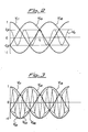
- Figure 2 illustrates the balanced three phase voltage waveforms vs time and the amplitude limit of a conventional HSFC converter;
- Figure 3 shows the output voltage waveforms of a converter according to the invention; and
- Figures 4A, 4B, 5A, 5B illustrate the flowcharts of a digital embodiment of the control circuit according to the invention.
- The direct converter shown in Figure 1 comprises two main portions, more precisely a plurality of controlled electronic switches SW1...SWS arranged to form a switch matrix MU, and a control circuit supplying the necessary control or drive signals to the switches, illustrated in the remaining portion of the drawing. The converter is connected between a three phase input voltage system LI through a filter I, and a three phase output voltage system LU through a filter U. In this case, the matrix MU consists of nine switches which connect any given input conductor with all output conductors. More generally, for polyphase systems with n input lines and m output lines, the switch matrix consists of nxm switches. Such switches must be adequate to withstand the maximum supply voltage as well as the maximum load current.
- For a better understanding of the working of the control circuit it will now be described the method according to which the apparatus works. For simplicity sake, the synthesis of one output phase voltage is considered, namely Voi.
- The corresponding output phase conductor can be connected with all the input conductors through the switches SW1, SW2, SW3 out of the SW1...SW9 switches of the matrix. Such switches are cyclically operated, i.e. closed, at a frequency fc, where fc is substantially higher (e.g. 10 times) than the highest of both the input and output frequencies, and in such a way that at any time one and only one of SW1, SW2, SW3 is closed. As the
cycle time 1/fo is very short, the three input voltages do not vary appreciably during the switching cycle. - Now let t be any given instant within a switching cycle Tc; m11(t), m12(t), m13(t) be the ratios between the time during which the output conductor (1) is connected to the corresponding input conductor (1, or 3) and the overall switching cycle Tc, i.e. the duty cycles of SW1, SW2, SW3 within the cycle T. As an example their values could be the following: m11(t)=0.4; m12(t)=0.35; m13(t)=0.25. If V11, V12, V,3 are the three input voltages during Tc, as measured with respect to the neutral input conductor N,, then the output waveform consists of three samples of the input voltages and will have an average amplitude, within Tc, approximately equal to:

- Consequently, if the above duty cycles mih(t) are modulated in a way to obtain a predetermined function Voav(t), typically sinusoidal, at frequency substantially lower than fc, the resulting actual output waveform Fourier spectrum consists of a low frequency component approximately equal to Voav(t) and of a cluster of undesired harmonics at frequencies comparable or higher than fe.
- Since such high frequency harmonics are usually acceptable and can anyway be filtered away fairly easily, the general method summarily described so far allows for the realization of a frequency converter, subject to the only limitation that output voltage Voav(t) cannot, at any time, exceed the range of the input voltage system. In fact, and with reference to the three phase system of waveforms shown in Figure 2, there is a time t in which the maximum positive voltage available is only 2 of input peak voltage. Hence the amplitude limitation of the HSFC converter that the output amplitude is lower or equal to ½ of the input amplitude.
- According the present invention, such limitation is overcome in view of the fact that the neutral conductor No of the output system must not necessarily be connected to the one N, of the input system. Consequently, it is no longer requested that outputs are sinusoidal with respect to the input system, as in the HSFC. The only condition to be met by the output waveforms is actually that the phase to phase voltages, i.e. the differences between any two output voltages, be sinusoidal and balanced.
- In particular, according to the invention, the output waveforms amplitudes as referenced to the input neutral conductor, are the following:

- These waveforms represent a sinusoidal, balanced output system since the phase to phase output voltages are:

- Contrarily to the situation of the HSFC converter wherein the synthetized waveforms are proportional to the first term only of the relationships (1), the waveforms represented in (1) allow for maximizing the output phase to phase voltages (2) without exceeding the fundamental limitation of this type of converter, with respect to the range of the input voltages.
- Namely, with reference to Figure 3, one can note that when in the (1) p is set equal to 1 and vo equal to V3/2 the waveforms (1) never exceed the range of the three input voltages, although they represent a three phase voltage system wherein the output phase to phase amplitude is V3/2 the input amplitude, i.e. considerably higher if compared with the limit of the prior art.
- With reference to the relations (1) it can be noted that anyone of the output voltages (e.g. Voi) as measured between the corresponding phase conductor and the input neutral conductor, comprises the usual component at the desired output frequency (vocos(wo(t)) with the proper phase angle, and a common term given by
-

- In the general case of an n phase input system and an m phase output system, the common term will be a linear combination of two sinusoidal waveforms, one having a frequency which is m times the output frequency, and the other having a frequency which is n times the input frequency.
- The converter of the present invention is therefore capable of synthesizing waveforms of the type represented in (1). Such waveforms are synthetized as follows:
- -Let w, v,, so be the input pulsation, amplitude and output load phase angle, respectively;
- -Let wo, vo, s, be the desired output pulsation and amplitude and the desired input phase angle respectively;
- -Let z(Y) be a function of time defined as:


- -Let M(t) be a matrix in which its elements mk,h(t) represent the duty cycle of the switch connecting the input line h with the output line k; -Define the function of time:


- Then if the nine switches SW1...SW9 (Figure 1) are driven so that:


- The so controlled converter is able to synthetize, on each output conductor a voltage waveform which, as measured with respect to the input neutral conductor, is expressed by the (1). Relationship (12) represents anyone of the three voltages of relationship (1) when using the compact notation given by (3). Relationship (13) represents, with the same notation, the input current of phase h.
- It is 'further to be pointed out that contrarily to the cited prior art, the ratio S between the trigonometrical tangents of the input and output phase displacements can be greater than 1 since this does not lead to values of the duty cycle, as expressed by mk,h(t), that are either negative or higher than 1. Therefore the controllable range of the input-output phase displacement is greatly enlarged.
- A non-limiting embodiment of the control circuit capable of generating drive signals according to (6)...(11) is now described with reference to Figure 1. Said control circuit converts the input control variables such as desired output frequency, amplitude and ratio between tangents of input and output phase displacement, into the appropriate drive signals for the power switches in MU.
- For the described embodiment providing for a three phase system both in input and output, the control circuit in its simplest form has four input control lines and nine output control lines. The input control signals are the desired ratio between the output and input voltages vo/vi, the desired ratio tg(s,)/tg(so), the desired output frequency and the actual input frequency; the output control signals are the drive pulses for the matrix MU.
said control circuit can be either an analog one (Figure 1) or a digital one (Figures 4A, 4B, 5A, 5B). - The operation of the analog control circuit is now described.
- The output frequency is set through the circuit Q1 comprising a voltage source and a potentiometer. A voltage controlled oscillator VC converts said voltage into an AC voltage having the frequency equal to the desired one (wo) and an AC voltage having a frequency which is three times the former (3wo). The input frequency is sensed on LI, shaped and squared by filter F. With this signal, the phase locked loop PL7 generates two synchronous AC voltages with frequency two and four times the input frequency (2w, and 4w,).
- The outputs of phase locked loops PL1...PL6 are three phase, sinusoidal with controllable amplitude, and can be synchronized on the sum or the difference of two input frequencies. By connecting the five mentioned AC signals (wo, 3wo, w,, 2w, and 4w,) to the inputs of the PL's, all of the sinusoidal components of M(t) can be obtained.
- The desired ratio between input and output phase displacements, S=tg(sl)/tg(so) is set by the circuit Q2 comprising two voltage sources and a potentiometer. This ratio can be negative and is not restricted in principle. The so obtained signal proportional to S is fed to a comparator C1 and a rectifier R1. The output from R1 is therefore proportional to |S|.
- The desired ratio vo/v, between output amplitude and input amplitude is set by circuit Q4 comprising a voltage source and a potentiometer. The network comprising X1 and A1, a multiplier and an amplifier respectively, result in a signal proportional to a according to (8), while adder/amplifier A2 together with multiplier X2 provide a signal proportional to p according to (9).
- This signal is fed to amplifiers A5, A6 to control the amplitudes of PL3, PL4, while its absolute value, obtained by rectifier R2, is used to control the amplitude_of PL5 and PL6 through amplifiers A7, A8. The voltage gains of A5...A8 are proportional to
-

- Moreover, signal a and the value zero are fed to multiplexer M in direct and reverse sequence, M being controlled by C1 so that signals a1, a2 according to (10) are available on the multiplexed outputs of M. Such outputs are fed to adders A3, A4 together with signal p and the resulting outputs control PL1, PL2 amplitudes according to (6).
- . The eighteen signals provided by PL1...PL6 are proportional to the sinusoidal components which form the duty cycle coefficients mk,h(t) according to (6)...(11). These signals are combined, in the correct order, by adders S1...S9 which output signals, proportional to mk,h(t) as given by (11), also providing the fixed offset required by (6). Such outputs are converted into drive pulses by programmable timers T1...T9 whose output pulse durations are proportional to the amplitude fed at the programming input.
- To obtain the required sequential operation, the timers are connected in rings of three units, where each group is connected to a single output line, in such a way that the end of each timer cycle would trigger the start of the next timer. By this arrangement, the condition that only one input conductor is connected at any given output conductor in any given time is fulfilled and overload on the switches is avoided.
- Timer outputs are decoupled and amplified by driver circuits D1...D9 which drive the power switches SW1...SW9 in the power switch matrix.
- The converter can be completed by optional input and output filters I and U, capacitive and inductive respectively, which may be required with high impedance supply or with non-inductive loads.
- An alternative embodiment of the control circuit based on a programmed digital circuit, is summarily described in the following. Reference is made to Figures 4A, 4B, 5A, 5B.
- In this type of embodiment, a digital processor is used to compute and evaluate the numerical values of matrix (11) at regular intervals, much shorter anyway than the duration of both input and output cycles. For example, in an application where both input and output frequencies are below 100 Hz, the matrix M(t) can be evaluated once every millisecond.
- The program of the processor consists of an initialization routine (Figure 4A) which upon processor start up or on interrupt whenever the control parameters are changed, inputs the values of w,, wo, v,, vo, S and evaluates constants a,, a2, p according to (8) (9) (10). Two subroutines (Figures 4B, 5A) can be defined to simplify the main program. The first one (Figure 4B) generates the function ZO(y)(t) as defined by (3) whereas the second one (Figure 5A) generates function m(x1,...,x6) as defined by (6). After the execution of the control is returned to the main program.
- In each evaluation cycle, (Figure 5B), the processor timer updates the time register t, and evaluates M(t) with the mentioned subroutines. The nine numbers thus obtained are then fed to digital to time duration converters or down counters, which drive in sequence, through driver circuits, the nine power switches in MU as described before.
- The power switches which form MU can be realized in many already known ways, for example as described in the cited U.S. Patent, or with newer components such as bidirectional power MOSFETs or COMFETs.
Claims (3)


Applications Claiming Priority (2)
| Application Number | Priority Date | Filing Date | Title |
|---|---|---|---|
| IT2400883 | 1983-12-05 | ||
| IT24008/83A IT1167285B (en) | 1983-12-05 | 1983-12-05 | METHOD AND EQUIPMENT FOR THE CONVERSION OF A POLYPHASE VOLTAGE SYSTEM |
Publications (3)
| Publication Number | Publication Date |
|---|---|
| EP0146032A2 EP0146032A2 (en) | 1985-06-26 |
| EP0146032A3 EP0146032A3 (en) | 1985-08-28 |
| EP0146032B1 true EP0146032B1 (en) | 1988-07-06 |
Family
ID=11211455
Family Applications (1)
| Application Number | Title | Priority Date | Filing Date |
|---|---|---|---|
| EP84114357A Expired EP0146032B1 (en) | 1983-12-05 | 1984-11-26 | Method and apparatus for the conversion of a polyphase voltage system |
Country Status (4)
| Country | Link |
|---|---|
| US (1) | US4628425A (en) |
| EP (1) | EP0146032B1 (en) |
| DE (1) | DE3472605D1 (en) |
| IT (1) | IT1167285B (en) |
Cited By (1)
| Publication number | Priority date | Publication date | Assignee | Title |
|---|---|---|---|---|
| EP3285386A1 (en) | 2016-08-10 | 2018-02-21 | Phase Motion Control S.p.A. | Matrix direct ac/ac converter |
Families Citing this family (9)
| Publication number | Priority date | Publication date | Assignee | Title |
|---|---|---|---|---|
| US5101899A (en) * | 1989-12-14 | 1992-04-07 | International Royal & Oil Company | Recovery of petroleum by electro-mechanical vibration |
| US5747972A (en) * | 1995-01-11 | 1998-05-05 | Microplanet Ltd. | Method and apparatus for electronic power control |
| US7315151B2 (en) * | 1995-01-11 | 2008-01-01 | Microplanet Inc. | Method and apparatus for electronic power control |
| US6328102B1 (en) | 1995-12-01 | 2001-12-11 | John C. Dean | Method and apparatus for piezoelectric transport |
| US5909367A (en) * | 1997-06-02 | 1999-06-01 | Reliance Electric Industrial Company | Modular AC-AC variable voltage and variable frequency power conveter system and control |
| US6995992B2 (en) * | 2003-06-20 | 2006-02-07 | Wisconsin Alumni Research Foundation | Dual bridge matrix converter |
| US6982890B2 (en) * | 2003-10-09 | 2006-01-03 | Wisconsin Alumni Research Foundation | Three phase isolated vector switching AC to AC frequency converters |
| DE102004004369A1 (en) * | 2004-01-29 | 2005-08-18 | Jungheinrich Ag | battery charger |
| DE102004016464A1 (en) * | 2004-03-31 | 2005-11-03 | Alstom Technology Ltd | Method for calculating and assessing the frequency spectrum of a matrix converter |
Citations (1)
| Publication number | Priority date | Publication date | Assignee | Title |
|---|---|---|---|---|
| EP0124302A2 (en) * | 1983-04-06 | 1984-11-07 | Texas Instruments Incorporated | A.C. supply converter |
Family Cites Families (9)
| Publication number | Priority date | Publication date | Assignee | Title |
|---|---|---|---|---|
| CA826777A (en) * | 1959-07-06 | 1969-11-04 | F. Blake Richard | Controlled frequency power supply system |
| US3170107A (en) * | 1960-05-02 | 1965-02-16 | Westinghouse Electric Corp | Controlled frequency alternating current system |
| US3585489A (en) * | 1969-06-20 | 1971-06-15 | Westinghouse Electric Corp | A low-frequency ac reference generator with inherently balanced controllable output voltage |
| US3999112A (en) * | 1975-05-08 | 1976-12-21 | Westinghouse Electric Corporation | Polyphase frequency converter |
| US4041368A (en) * | 1976-01-02 | 1977-08-09 | Borg-Warner Corporation | Three-phase, quasi-square wave VSCF induction generator system |
| IT1111993B (en) * | 1979-03-06 | 1986-01-13 | Venturini Marco | DIRECT AC / AC FREQUENCY CONVERTER |
| US4352155A (en) * | 1981-08-14 | 1982-09-28 | Westinghouse Electric Corp. | Variable speed constant frequency power converter with two modes of operation |
| US4439823A (en) * | 1982-01-11 | 1984-03-27 | Westinghouse Electric Corp. | Converting multiphase power from one frequency to another using current waveforms |
| GB2113485A (en) * | 1982-01-13 | 1983-08-03 | Texas Instruments Ltd | An a.c. supply converter |
-
1983
- 1983-12-05 IT IT24008/83A patent/IT1167285B/en active
-
1984
- 1984-11-26 DE DE8484114357T patent/DE3472605D1/en not_active Expired
- 1984-11-26 EP EP84114357A patent/EP0146032B1/en not_active Expired
- 1984-11-26 US US06/674,929 patent/US4628425A/en not_active Expired - Fee Related
Patent Citations (1)
| Publication number | Priority date | Publication date | Assignee | Title |
|---|---|---|---|---|
| EP0124302A2 (en) * | 1983-04-06 | 1984-11-07 | Texas Instruments Incorporated | A.C. supply converter |
Cited By (1)
| Publication number | Priority date | Publication date | Assignee | Title |
|---|---|---|---|---|
| EP3285386A1 (en) | 2016-08-10 | 2018-02-21 | Phase Motion Control S.p.A. | Matrix direct ac/ac converter |
Also Published As
| Publication number | Publication date |
|---|---|
| EP0146032A3 (en) | 1985-08-28 |
| EP0146032A2 (en) | 1985-06-26 |
| IT8324008A0 (en) | 1983-12-05 |
| IT1167285B (en) | 1987-05-13 |
| DE3472605D1 (en) | 1988-08-11 |
| US4628425A (en) | 1986-12-09 |
Similar Documents
| Publication | Publication Date | Title |
|---|---|---|
| US6154378A (en) | Polyphase inverter with neutral-leg inductor | |
| US4468725A (en) | Direct AC converter for converting a balanced AC polyphase input to an output voltage | |
| CA2174295C (en) | Voltage source type power converting apparatus | |
| EP0146032B1 (en) | Method and apparatus for the conversion of a polyphase voltage system | |
| US3775663A (en) | Inverter with electronically controlled neutral terminal | |
| EP0124302A2 (en) | A.C. supply converter | |
| EP0473257B1 (en) | Power conversion scheme employing paralleled units | |
| KR20020030261A (en) | Method for operating a matrix converter and matrix converter for implementing the method | |
| JPH07501439A (en) | VSCF device that reduces DC link ripple | |
| US20080247211A1 (en) | Active generator control sequence | |
| US5132892A (en) | PWM controller used in a multiple inverter | |
| KR890004589B1 (en) | Frequency converter apparatus | |
| EP0072527A2 (en) | Variable speed constant frequency power converter with two modes of operation | |
| GB2048588A (en) | Direct A.C. to A.C. converter | |
| US5523937A (en) | Frequency converter, procedure for controlling it and motor control using a frequency converter | |
| Watthanasam et al. | Analysis and DSP-based implementation of modulation algorithms for AC-AC matrix converters | |
| JPS6455076A (en) | Feeding system using polyphase multiple pwm inverter | |
| Zhang et al. | An efficient space vector modulation algorithm for AC-AC matrix converters: analysis and implementation | |
| US3988660A (en) | Circuit for rectifying a three-phase alternating signal | |
| Schuster | A drive-system with a digitally controlled matrix-converter feeding an AC-induction machine | |
| RU2279178C1 (en) | Three-phased controllable rectifier | |
| JP2561918B2 (en) | PWM method for transformer multiple inverter | |
| Vickers et al. | Matrix converter application for direct-drive gas turbine generator sets | |
| SU983970A1 (en) | Device for control of pulse converter | |
| Dar’enkov et al. | Matrix Converter U/f Control Method for Electric Drive of Fluid-Handling Application |
Legal Events
| Date | Code | Title | Description |
|---|---|---|---|
| PUAI | Public reference made under article 153(3) epc to a published international application that has entered the european phase |
Free format text: ORIGINAL CODE: 0009012 |
|
| PUAL | Search report despatched |
Free format text: ORIGINAL CODE: 0009013 |
|
| AK | Designated contracting states |
Designated state(s): DE FR GB |
|
| AK | Designated contracting states |
Designated state(s): DE FR GB |
|
| 17P | Request for examination filed |
Effective date: 19860217 |
|
| 17Q | First examination report despatched |
Effective date: 19870217 |
|
| GRAA | (expected) grant |
Free format text: ORIGINAL CODE: 0009210 |
|
| AK | Designated contracting states |
Kind code of ref document: B1 Designated state(s): DE FR GB |
|
| REF | Corresponds to: |
Ref document number: 3472605 Country of ref document: DE Date of ref document: 19880811 |
|
| ET | Fr: translation filed | ||
| PLBE | No opposition filed within time limit |
Free format text: ORIGINAL CODE: 0009261 |
|
| STAA | Information on the status of an ep patent application or granted ep patent |
Free format text: STATUS: NO OPPOSITION FILED WITHIN TIME LIMIT |
|
| 26N | No opposition filed | ||
| PGFP | Annual fee paid to national office [announced via postgrant information from national office to epo] |
Ref country code: GB Payment date: 19901113 Year of fee payment: 7 |
|
| PG25 | Lapsed in a contracting state [announced via postgrant information from national office to epo] |
Ref country code: GB Effective date: 19911126 |
|
| GBPC | Gb: european patent ceased through non-payment of renewal fee | ||
| PGFP | Annual fee paid to national office [announced via postgrant information from national office to epo] |
Ref country code: FR Payment date: 19931126 Year of fee payment: 10 |
|
| PGFP | Annual fee paid to national office [announced via postgrant information from national office to epo] |
Ref country code: DE Payment date: 19940126 Year of fee payment: 10 |
|
| PG25 | Lapsed in a contracting state [announced via postgrant information from national office to epo] |
Ref country code: FR Effective date: 19950731 |
|
| PG25 | Lapsed in a contracting state [announced via postgrant information from national office to epo] |
Ref country code: DE Effective date: 19950801 |
|
| REG | Reference to a national code |
Ref country code: FR Ref legal event code: ST |