EP0148687B1 - Photosensitive device with opaque radiation zones among the detectors, and method of manufacture - Google Patents
Photosensitive device with opaque radiation zones among the detectors, and method of manufacture Download PDFInfo
- Publication number
- EP0148687B1 EP0148687B1 EP84402637A EP84402637A EP0148687B1 EP 0148687 B1 EP0148687 B1 EP 0148687B1 EP 84402637 A EP84402637 A EP 84402637A EP 84402637 A EP84402637 A EP 84402637A EP 0148687 B1 EP0148687 B1 EP 0148687B1
- Authority
- EP
- European Patent Office
- Prior art keywords
- layer
- opaque
- radiation
- metal
- detected
- Prior art date
- Legal status (The legal status is an assumption and is not a legal conclusion. Google has not performed a legal analysis and makes no representation as to the accuracy of the status listed.)
- Expired
Links
- 230000005855 radiation Effects 0.000 title claims description 30
- 238000004519 manufacturing process Methods 0.000 title claims description 5
- 238000000034 method Methods 0.000 title claims 7
- 239000000758 substrate Substances 0.000 claims description 24
- 229910052751 metal Inorganic materials 0.000 claims description 20
- 239000002184 metal Substances 0.000 claims description 20
- 239000010407 anodic oxide Substances 0.000 claims description 10
- 238000000151 deposition Methods 0.000 claims description 6
- 230000008021 deposition Effects 0.000 claims description 6
- PCHJSUWPFVWCPO-UHFFFAOYSA-N gold Chemical compound [Au] PCHJSUWPFVWCPO-UHFFFAOYSA-N 0.000 claims description 5
- 229910052737 gold Inorganic materials 0.000 claims description 5
- 239000010931 gold Substances 0.000 claims description 5
- 239000011347 resin Substances 0.000 claims description 5
- 229920005989 resin Polymers 0.000 claims description 5
- PXHVJJICTQNCMI-UHFFFAOYSA-N Nickel Chemical compound [Ni] PXHVJJICTQNCMI-UHFFFAOYSA-N 0.000 claims description 4
- 239000003989 dielectric material Substances 0.000 claims description 4
- 238000001704 evaporation Methods 0.000 claims description 4
- 230000008020 evaporation Effects 0.000 claims description 4
- WPYVAWXEWQSOGY-UHFFFAOYSA-N indium antimonide Chemical compound [Sb]#[In] WPYVAWXEWQSOGY-UHFFFAOYSA-N 0.000 claims description 4
- 229910052782 aluminium Inorganic materials 0.000 claims description 3
- XAGFODPZIPBFFR-UHFFFAOYSA-N aluminium Chemical compound [Al] XAGFODPZIPBFFR-UHFFFAOYSA-N 0.000 claims description 3
- 239000000463 material Substances 0.000 claims description 3
- 230000003647 oxidation Effects 0.000 claims description 3
- 238000007254 oxidation reaction Methods 0.000 claims description 3
- JBRZTFJDHDCESZ-UHFFFAOYSA-N AsGa Chemical compound [As]#[Ga] JBRZTFJDHDCESZ-UHFFFAOYSA-N 0.000 claims description 2
- VYZAMTAEIAYCRO-UHFFFAOYSA-N Chromium Chemical compound [Cr] VYZAMTAEIAYCRO-UHFFFAOYSA-N 0.000 claims description 2
- 229910001218 Gallium arsenide Inorganic materials 0.000 claims description 2
- GPXJNWSHGFTCBW-UHFFFAOYSA-N Indium phosphide Chemical compound [In]#P GPXJNWSHGFTCBW-UHFFFAOYSA-N 0.000 claims description 2
- RTAQQCXQSZGOHL-UHFFFAOYSA-N Titanium Chemical compound [Ti] RTAQQCXQSZGOHL-UHFFFAOYSA-N 0.000 claims description 2
- 238000005119 centrifugation Methods 0.000 claims description 2
- 229910052804 chromium Inorganic materials 0.000 claims description 2
- 239000011651 chromium Substances 0.000 claims description 2
- 150000001875 compounds Chemical class 0.000 claims description 2
- 229910052759 nickel Inorganic materials 0.000 claims description 2
- OCGWQDWYSQAFTO-UHFFFAOYSA-N tellanylidenelead Chemical compound [Pb]=[Te] OCGWQDWYSQAFTO-UHFFFAOYSA-N 0.000 claims description 2
- 229910052719 titanium Inorganic materials 0.000 claims description 2
- 239000010936 titanium Substances 0.000 claims description 2
- 238000010298 pulverizing process Methods 0.000 claims 2
- UGFAIRIUMAVXCW-UHFFFAOYSA-N Carbon monoxide Chemical compound [O+]#[C-] UGFAIRIUMAVXCW-UHFFFAOYSA-N 0.000 claims 1
- XUIMIQQOPSSXEZ-UHFFFAOYSA-N Silicon Chemical compound [Si] XUIMIQQOPSSXEZ-UHFFFAOYSA-N 0.000 claims 1
- 239000004411 aluminium Substances 0.000 claims 1
- 238000007598 dipping method Methods 0.000 claims 1
- 150000002500 ions Chemical class 0.000 claims 1
- WYUZTTNXJUJWQQ-UHFFFAOYSA-N tin telluride Chemical compound [Te]=[Sn] WYUZTTNXJUJWQQ-UHFFFAOYSA-N 0.000 claims 1
- 239000004065 semiconductor Substances 0.000 description 11
- 230000000694 effects Effects 0.000 description 5
- 229910003437 indium oxide Inorganic materials 0.000 description 3
- PJXISJQVUVHSOJ-UHFFFAOYSA-N indium(iii) oxide Chemical class [O-2].[O-2].[O-2].[In+3].[In+3] PJXISJQVUVHSOJ-UHFFFAOYSA-N 0.000 description 3
- 230000015556 catabolic process Effects 0.000 description 2
- 238000009792 diffusion process Methods 0.000 description 2
- -1 ln Sb Substances 0.000 description 2
- 238000000206 photolithography Methods 0.000 description 2
- LIVNPJMFVYWSIS-UHFFFAOYSA-N silicon monoxide Chemical compound [Si-]#[O+] LIVNPJMFVYWSIS-UHFFFAOYSA-N 0.000 description 2
- 238000004544 sputter deposition Methods 0.000 description 2
- 238000007738 vacuum evaporation Methods 0.000 description 2
- MARUHZGHZWCEQU-UHFFFAOYSA-N 5-phenyl-2h-tetrazole Chemical compound C1=CC=CC=C1C1=NNN=N1 MARUHZGHZWCEQU-UHFFFAOYSA-N 0.000 description 1
- ZOKXTWBITQBERF-UHFFFAOYSA-N Molybdenum Chemical compound [Mo] ZOKXTWBITQBERF-UHFFFAOYSA-N 0.000 description 1
- KWYUFKZDYYNOTN-UHFFFAOYSA-M Potassium hydroxide Chemical compound [OH-].[K+] KWYUFKZDYYNOTN-UHFFFAOYSA-M 0.000 description 1
- ATJFFYVFTNAWJD-UHFFFAOYSA-N Tin Chemical compound [Sn] ATJFFYVFTNAWJD-UHFFFAOYSA-N 0.000 description 1
- 240000008042 Zea mays Species 0.000 description 1
- FYEOSUFWPIXZOR-UHFFFAOYSA-N [bis(selanylidene)-$l^{5}-arsanyl]selanyl-bis(selanylidene)-$l^{5}-arsane Chemical compound [Se]=[As](=[Se])[Se][As](=[Se])=[Se] FYEOSUFWPIXZOR-UHFFFAOYSA-N 0.000 description 1
- 238000010521 absorption reaction Methods 0.000 description 1
- 239000000969 carrier Substances 0.000 description 1
- 210000004027 cell Anatomy 0.000 description 1
- 230000008878 coupling Effects 0.000 description 1
- 238000010168 coupling process Methods 0.000 description 1
- 238000005859 coupling reaction Methods 0.000 description 1
- 238000005868 electrolysis reaction Methods 0.000 description 1
- 229910052738 indium Inorganic materials 0.000 description 1
- APFVFJFRJDLVQX-UHFFFAOYSA-N indium atom Chemical compound [In] APFVFJFRJDLVQX-UHFFFAOYSA-N 0.000 description 1
- 230000006698 induction Effects 0.000 description 1
- 239000011810 insulating material Substances 0.000 description 1
- QSHDDOUJBYECFT-UHFFFAOYSA-N mercury Chemical compound [Hg] QSHDDOUJBYECFT-UHFFFAOYSA-N 0.000 description 1
- 229910052753 mercury Inorganic materials 0.000 description 1
- 150000002739 metals Chemical class 0.000 description 1
- 229910052750 molybdenum Inorganic materials 0.000 description 1
- 239000011733 molybdenum Substances 0.000 description 1
- 230000003287 optical effect Effects 0.000 description 1
- BASFCYQUMIYNBI-UHFFFAOYSA-N platinum Chemical compound [Pt] BASFCYQUMIYNBI-UHFFFAOYSA-N 0.000 description 1
- 230000035945 sensitivity Effects 0.000 description 1
- 230000006641 stabilisation Effects 0.000 description 1
- 238000011105 stabilization Methods 0.000 description 1
- 229910052714 tellurium Inorganic materials 0.000 description 1
- PORWMNRCUJJQNO-UHFFFAOYSA-N tellurium atom Chemical compound [Te] PORWMNRCUJJQNO-UHFFFAOYSA-N 0.000 description 1
Images
Classifications
-
- H—ELECTRICITY
- H01—ELECTRIC ELEMENTS
- H01L—SEMICONDUCTOR DEVICES NOT COVERED BY CLASS H10
- H01L27/00—Devices consisting of a plurality of semiconductor or other solid-state components formed in or on a common substrate
- H01L27/14—Devices consisting of a plurality of semiconductor or other solid-state components formed in or on a common substrate including semiconductor components sensitive to infrared radiation, light, electromagnetic radiation of shorter wavelength or corpuscular radiation and specially adapted either for the conversion of the energy of such radiation into electrical energy or for the control of electrical energy by such radiation
- H01L27/144—Devices controlled by radiation
- H01L27/1446—Devices controlled by radiation in a repetitive configuration
-
- H—ELECTRICITY
- H01—ELECTRIC ELEMENTS
- H01L—SEMICONDUCTOR DEVICES NOT COVERED BY CLASS H10
- H01L27/00—Devices consisting of a plurality of semiconductor or other solid-state components formed in or on a common substrate
- H01L27/14—Devices consisting of a plurality of semiconductor or other solid-state components formed in or on a common substrate including semiconductor components sensitive to infrared radiation, light, electromagnetic radiation of shorter wavelength or corpuscular radiation and specially adapted either for the conversion of the energy of such radiation into electrical energy or for the control of electrical energy by such radiation
- H01L27/144—Devices controlled by radiation
- H01L27/146—Imager structures
- H01L27/14643—Photodiode arrays; MOS imagers
- H01L27/14649—Infrared imagers
-
- H—ELECTRICITY
- H01—ELECTRIC ELEMENTS
- H01L—SEMICONDUCTOR DEVICES NOT COVERED BY CLASS H10
- H01L31/00—Semiconductor devices sensitive to infrared radiation, light, electromagnetic radiation of shorter wavelength or corpuscular radiation and specially adapted either for the conversion of the energy of such radiation into electrical energy or for the control of electrical energy by such radiation; Processes or apparatus specially adapted for the manufacture or treatment thereof or of parts thereof; Details thereof
- H01L31/02—Details
- H01L31/0216—Coatings
- H01L31/02161—Coatings for devices characterised by at least one potential jump barrier or surface barrier
- H01L31/02162—Coatings for devices characterised by at least one potential jump barrier or surface barrier for filtering or shielding light, e.g. multicolour filters for photodetectors
- H01L31/02164—Coatings for devices characterised by at least one potential jump barrier or surface barrier for filtering or shielding light, e.g. multicolour filters for photodetectors for shielding light, e.g. light blocking layers, cold shields for infrared detectors
-
- Y—GENERAL TAGGING OF NEW TECHNOLOGICAL DEVELOPMENTS; GENERAL TAGGING OF CROSS-SECTIONAL TECHNOLOGIES SPANNING OVER SEVERAL SECTIONS OF THE IPC; TECHNICAL SUBJECTS COVERED BY FORMER USPC CROSS-REFERENCE ART COLLECTIONS [XRACs] AND DIGESTS
- Y10—TECHNICAL SUBJECTS COVERED BY FORMER USPC
- Y10S—TECHNICAL SUBJECTS COVERED BY FORMER USPC CROSS-REFERENCE ART COLLECTIONS [XRACs] AND DIGESTS
- Y10S148/00—Metal treatment
- Y10S148/118—Oxide films
-
- Y—GENERAL TAGGING OF NEW TECHNOLOGICAL DEVELOPMENTS; GENERAL TAGGING OF CROSS-SECTIONAL TECHNOLOGIES SPANNING OVER SEVERAL SECTIONS OF THE IPC; TECHNICAL SUBJECTS COVERED BY FORMER USPC CROSS-REFERENCE ART COLLECTIONS [XRACs] AND DIGESTS
- Y10—TECHNICAL SUBJECTS COVERED BY FORMER USPC
- Y10S—TECHNICAL SUBJECTS COVERED BY FORMER USPC CROSS-REFERENCE ART COLLECTIONS [XRACs] AND DIGESTS
- Y10S257/00—Active solid-state devices, e.g. transistors, solid-state diodes
- Y10S257/906—Dram with capacitor electrodes used for accessing, e.g. bit line is capacitor plate
Definitions
- the present invention relates to a photosensitive device comprising between the detectors areas opaque to the radiation to be detected. It also relates to a method of manufacturing such a device.
- the detectors in question are generally photo-diodes or photo-MOS, integrated in the same semiconductor substrate.
- This "edge effect” manifests itself in particular in semiconductor substrates sensitive to infrared radiation. It is either binary materials such as indium antimonide, ln Sb, lead tellurium, Pb Te ..., or ternary materials such as mercury and cadmium telluride, Cd Hg Te or tin and lead telluride, Pb Sn Te.
- This "edge effect” is observed more generally when a semiconductor substrate with high mobility is used; this is the case for example of semiconductors, consisting of compounds of the families Ili and V, such as gallium arsenide, As Ga, or indium phosphide, P In.
- junctions are made in the semiconductor substrate which is covered with oxide. Through windows pierced through the oxide, electrodes are deposited in contact with the substrate. These electrodes are subjected to a potential and at the same time their geometry determines that of the zones opaque to the radiation separating the detectors.
- the present invention relates to a photosensitive device comprising between the detectors of the areas opaque to radiation which eliminates the drawbacks, of solutions known from the prior art.
- the device according to the invention is not obtained by self-indexing as is the case for the device of application EP-A-0 024 970.
- the invention makes it possible to vary the surface of the photosensitive detectors without difficulty.
- a first layer of anodic oxide covering the entire semiconductor substrate allows perfect stabilization of the photo-voltaic junctions. This is due to the qualities specific to anodic oxides; in particular, a thin oxide layer, around 10 to 60 nm (100 to 600 A), for example, is sufficient to obtain these results.
- the device according to the invention it is possible without difficulty to cover the edges of the junctions, since the first insulating layer extends over the entire substrate and the second layer, opaque to the radiation to be detected, is etched by photo-lithography, which allows you to freely choose the areas where you want to keep this second layer.
- the second metal layer receives no voltage and is covered by an insulating layer.
- an avahtage of the device according to the invention is that the areas opaque to radiation have an insulating surface which can be used without risk of short circuit for the passage of various connections.
- the device according to the invention makes it possible to bring two photodiodes 50 ⁇ m apart from each other without too much intermodulation problem, whereas in the prior art at least 100 are required. ⁇ m.
- These figures correspond to the example of a semiconductor substrate of indium antimonide, type N, placed at 77 degrees Kelvin, comprising 5.10 15 carriers of majority charges per cubic centimeter, for which the lifetime of the holes is approximately 2.10- 7 seconds, their mobility is approximately 4000 cm 2 per Volt and per second, which corresponds to a diffusion coefficient of approximately 26 cm 2 per second and to a diffusion length Lp of approximately 23 ⁇ m.
- the same example for a P type indium antimonide substrate shows that at a distance of 60 ⁇ m from the edge of a junction, the signal is practically zero.
- the device according to the invention makes it possible in this case to bring two photo-diodes of approximately 15 ⁇ m closer to each other.
- the device according to the invention therefore makes it possible to increase the resolution by bringing the detectors closer together, while limiting the optical coupling between the detectors.
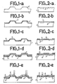
- FIGS. 1a to e and 2a to e represent various stages of a manufacturing process d 'An embodiment of a device according to the invention, in the case of a mesa structure in Figures 1a to e and das the case of a planar structure in Figures 2a to e.
- FIGS. 1a to e various stages of a method of manufacturing an embodiment of a device according to the invention have been shown.
- Photovoltaic junctions 2, of N / P or P / N type are symbolically represented in FIG. 1a by dotted lines on a semiconductor substrate 1.
- FIG. 1a diodes of the mesa type are shown.
- An oxide is grown by anodic oxidation over the entire surface of the substrate - see Figure 1b.
- This first layer of oxide bears the reference 3. Its thickness is approximately 10 to 60 nm (100 to 600 A).
- the growth of anodic oxide takes place, for example, by electrolysis.
- a semiconductor substrate made of indium atimoniide it is possible, for example, to immerse the substrate in a potassium hydroxide solution of which it constitutes the anode, while as cathode, a platinum wire is used for example.
- the oxide obtained is rich in indium oxides. It should be noted that the analysis of the product obtained reveals that the oxide deposition was carried out by anodic oxidation.
- indium oxide deposited by evaporation is conductive while anodic indium oxide is a very good dielectric.
- a second layer 4 opaque to the radiation to be detected is then deposited on the first layer of anode oxide 3 - see FIG. 1c.
- this second layer is not necessarily metallic.
- a body such as arsenic pentaselenide, A S2 Ses, is opaque to visible radiation.
- the second layer must be metallic, it may for example be made of gold or aluminum.
- a second layer 4 can be used, constituted by the superposition of at least first and second elementary metal layers.
- the first elementary metalic layer consists of a metal ensuring good contact, good "bonding", with the anodic oxide layer and with the second elementary metal layer.
- the second layer 4 opaque to the radiation to be detected can be formed by the superposition of several elementary layers.
- This second layer 4 is etched by photo-lithography for example, so as to cover only the areas which it is desired to make opaque to the radiation to be detected.
- Layer 4 can only be left between the detectors. It can also be left to extend over part of the detectors.
- This second layer has a thickness of about 100 to 600 nm (1000 to 6000 A) for example. It can be deposited for example by vacuum evaporation or sputtering.
- a third layer 5 - see FIG. 1d - is deposited in dielectric material, which covers the entire surface. It can be an organic isolate or not, for example negative photosensitive resin or silicon monoxide, Si 0.
- This last layer can be deposited for example by vacuum evaporation, cathode sputtering, ionic deposition, dip induction, centrifugation ...
- Its thickness can be, for example, of the order duum.
- metallic connections 6 can be made in contact with the junctions 2 through windows passing through the first and third layers. These connections 6 are arranged on the third layer 5. It is possible to use metal connections opaque to the radiation to be detected and which therefore modify the geometry of the photosensitive zones.
- Figures 2a to e differ from Figures 1a to e only because they show diodes with planar structure.
Description
La présente invention concerne un dispositif photosensible comportant entre les détecteurs des zones opaques au rayonnement à détecter. Elle concerne également un procédé de fabrication d'un tel dispositif.The present invention relates to a photosensitive device comprising between the detectors areas opaque to the radiation to be detected. It also relates to a method of manufacturing such a device.
Les détecteurs dont il est question sont généralement des photo-diodes ou des photo-MOS, intégrés dans un même substrat semi-conducteur.The detectors in question are generally photo-diodes or photo-MOS, integrated in the same semiconductor substrate.
Comme cela a été expliqué dans la demade de brevet EP-A-0 024 970 au nom de THOMSON-CSF, dans certaines applications, on est conduit à diminuer les dimensions des détecteurs. Il arrive alors que l'on constate "un effet de bord", c'est-à-dire que la zone sur laquelle le rayonnement reçu par un détecteur produit ses effets devienne sensiblement supérieure à la surface du détecteur, ce qui limite la dimension minimale que l'on peut consacrer à chaque détecteur.As explained in patent application EP-A-0 024 970 in the name of THOMSON-CSF, in certain applications, it is necessary to reduce the dimensions of the detectors. It sometimes happens that there is an "edge effect", that is to say that the area on which the radiation received by a detector produces its effects becomes significantly greater than the surface of the detector, which limits the dimension minimum that can be devoted to each detector.
Cet "effet de bord" se manifeste notamment dans les substrats semi-conducteurs sensibles au rayonnement infra-rouge. Il s'agit soit de matériaux binaires tels que l'antimoniure d'indium, ln Sb, le tellure de plomb, Pb Te..., soit de matériaux ternaires tels que le tellurure de mercure et de cadmium, Cd Hg Te ou le tellurure d'étain et de plomb, Pb Sn Te. On observe cet "effet de bord" d'une façon plus générale lorsqu'on utilise un substrat semi-conducteur à haute mobilité; c'est ainsi le cas par exemple des semi-conducteurs, constitués de composés des familles Ili et V, tels que l'arséniure de gallium, As Ga, ou le phosphure d'indium, P In.This "edge effect" manifests itself in particular in semiconductor substrates sensitive to infrared radiation. It is either binary materials such as indium antimonide, ln Sb, lead tellurium, Pb Te ..., or ternary materials such as mercury and cadmium telluride, Cd Hg Te or tin and lead telluride, Pb Sn Te. This "edge effect" is observed more generally when a semiconductor substrate with high mobility is used; this is the case for example of semiconductors, consisting of compounds of the families Ili and V, such as gallium arsenide, As Ga, or indium phosphide, P In.
Pour combattre cet "effet de bord", tout en conservant aux détecteurs de faibles dimenisons, diverses solutions ont été utilisées dans l'art antérieur pour créer entre les détecteurs des zones opaques au rayonnement à détecter.To combat this "edge effect", while keeping detectors small in size, various solutions have been used in the prior art to create between the detectors areas opaque to the radiation to be detected.
Dans la demade de brevet EP-A-0 024 970 déjà citée, on utilise comme masque pour réaliser ces zones opaques, la résine photosensible - référence 3 sur les figures 1 et 2 de ce brevet- servant à délimiter les zones réservées aux photo-diodes mésa. Cette solution présente les inconvénients suivants:
- - la géométrie des zones recouvertes de résine photosensible détermine impérativement les dimensions des zones opaques et celles des détecteurs;
- - on dépose une couche mince 5, opaque au rayonnement, par exemple par évaporation. Il peut s'agir d'une couche d'isolant, mais ce dépôt fait que l'isolant est chargé électriquement et que les jonctions photo-voltaïques des détecteurs ne sont pas stabilisées électriquement au maximum;
- - comme le dépôt des couches opaques au rayonnement se fait par auto-indexation sur les zones recouvertes de résine photosensible, il est impossible de cacher les bords des jonctions. Les détecteurs présentent donc une sensibilité accrue sur les bords des jonctions, ce qui est un inonvénient.
- - the geometry of the areas covered with photosensitive resin imperatively determines the dimensions of the opaque areas and those of the detectors;
- - A thin layer 5 is deposited, opaque to radiation, for example by evaporation. It may be an insulating layer, but this deposition means that the insulating material is electrically charged and that the photo-voltaic junctions of the detectors are not electrically stabilized to the maximum;
- - as the deposition of the layers opaque to radiation is done by self-indexing on the areas covered with photosensitive resin, it is impossible to hide the edges of the junctions. The detectors therefore have increased sensitivity at the edges of the junctions, which is a drawback.
Une autre solution connue de l'art antérieur est de réaliser des électrodes dites de champ.Another solution known from the prior art is to produce so-called field electrodes.
Dans ce cas, on realise des jonctions dans le substrat semi-conducteur que l'on recouvre d'oxyde. Par des fenêtres percées à travers l'oxyde, on dépose des électrodes en contact avec le substrat. Ces électrodes sont soumises à un potentiel et en même temps leur géométrie détermine celle des zones opaques au rayonnement séparant les détecteurs.In this case, junctions are made in the semiconductor substrate which is covered with oxide. Through windows pierced through the oxide, electrodes are deposited in contact with the substrate. These electrodes are subjected to a potential and at the same time their geometry determines that of the zones opaque to the radiation separating the detectors.
L'inconvénient de cette solution, ce sont les risques de claquage de l'oxyde, qui est intercalé entre le substrat semi-conducteur et l'électrode de champ qui sont portés à des potentiels différents.The drawback of this solution is the risk of breakdown of the oxide, which is interposed between the semiconductor substrate and the field electrode, which are brought to different potentials.
La présente invention concerne un dispositif photosensible comportat entre les detecteurs des zones opaques au rayonnement qui supprime les inconvénients, des solutions connues de l'art antérieur.The present invention relates to a photosensitive device comprising between the detectors of the areas opaque to radiation which eliminates the drawbacks, of solutions known from the prior art.
La présente invention concerne un dispositif photosensible comportant des détecteurs intégrés dans un même substrat semi-conducteur avec, entre tes détecteurs, des zones opaques au rayonnement à détecter, caractérisé en ce que la surface du substrat est recouverte des trois couches suivantes;
- - une première couche d'oxyde anodique qui recouvre toute la surface du substrat;
- - une deuxième couche, constituée par au moins une couche de métal opaque au rayonnement à détecter, qui ne recouvre que lesdites zones opaques au rayonnement;
- - une troisième couche en matériau diélectrique recouvrant toute la surface.
- - a first layer of anodic oxide which covers the entire surface of the substrate;
- - A second layer, consisting of at least one layer of metal opaque to the radiation to be detected, which covers only said areas opaque to radiation;
- - a third layer of dielectric material covering the entire surface.
Le dispositif selon l'invention n'est pas obtenu par auto-indexation comme c'est le cas pour le dispositif de la demande EP-A-0 024 970. L'invention permet de faire varier sans difficulté la surface des détecteurs photosensibles.The device according to the invention is not obtained by self-indexing as is the case for the device of application EP-A-0 024 970. The invention makes it possible to vary the surface of the photosensitive detectors without difficulty.
L'utilisation d'une première couche d'oxyde anodique recouvrant tout le substrat semi-conducteur permet une stabilisation parfaite des jonctions photo-voltaïques. Cela tient aux qualités propres aux oxydes anodiques; en particulier, il suffit d'une couche d'oxyde de faible épaisseur, d'environ 10 à 60 nm (100 à 600 A) par exemple, pour obtenir ces résultats.The use of a first layer of anodic oxide covering the entire semiconductor substrate allows perfect stabilization of the photo-voltaic junctions. This is due to the qualities specific to anodic oxides; in particular, a thin oxide layer, around 10 to 60 nm (100 to 600 A), for example, is sufficient to obtain these results.
Dans le dispositif selon l'invention, on peut sans difficulté recouvrir les bords des jontions, car la première couche isolante s'étend sur tout le substrat et la deuxième couche, opaque au rayonnement à détecter, est gravée par photo- lithogravure, ce qui permet de choisir librement les zones où l'on désire conserver cette deuxième couche.In the device according to the invention, it is possible without difficulty to cover the edges of the junctions, since the first insulating layer extends over the entire substrate and the second layer, opaque to the radiation to be detected, is etched by photo-lithography, which allows you to freely choose the areas where you want to keep this second layer.
Dans le dispositif selon l'invention, il n'y a pas de risque de claquage de la première couche isolante car la deuxième couche métallique ne reçoit pas de tension et se trouve recouverte par une couche isolante.In the device according to the invention, there is no risk of breakdown of the first insulating layer because the second metal layer receives no voltage and is covered by an insulating layer.
Enfin, un avahtage du dispositif selon l'invention est que les zones opaques au rayonnement présentent une surface isolante que l'on peut utiliser sans risque de court-circuit pour le passage de diverses connexions.Finally, an avahtage of the device according to the invention is that the areas opaque to radiation have an insulating surface which can be used without risk of short circuit for the passage of various connections.
Das un exemple d'utilisation bien déterminé, le dispositif selon l'invention permet de rapprocher deux photodiodes à 50 µm l'une de l'autre sans trop de problème d'intermodulation, alors que dans l'art antérieur il faut au moins 100 µm. Ces chiffres correspondent à l'exemple d'un substrat semi-conducteur en antimoniure d'indium, de type N, placé à 77 degrés Kelvin, comprenant 5.1015 porteurs de charges majoritaires par centimètre cube, pour lequel a durée de vie des trous est d'environ 2.10-7 secondes, leur mobilité est d'environ 4000 cm2 par Volt et par seconde, ce qui correspond à un coefficient de diffusion denviron 26 cm2 par seconde et à une longueur de diffusion Lp d'environ 23 µm. On admet dans cet exemple une loi de décroissance du signal en fonction de la distance x au point d'absorption d'un photon de ta forme: 1 = lo.e-x/Lp. A une distance de 60 µm du bord d'une jontion, le signal est encore égal à 0,07. 10; le dispositf selon l'invention permet donc de rapprocher deux photodiodes à 50 µm l'une de l'autre sans problème.In a well-defined example of use, the device according to the invention makes it possible to bring two photodiodes 50 μm apart from each other without too much intermodulation problem, whereas in the prior art at least 100 are required. µm. These figures correspond to the example of a semiconductor substrate of indium antimonide, type N, placed at 77 degrees Kelvin, comprising 5.10 15 carriers of majority charges per cubic centimeter, for which the lifetime of the holes is approximately 2.10- 7 seconds, their mobility is approximately 4000 cm 2 per Volt and per second, which corresponds to a diffusion coefficient of approximately 26 cm 2 per second and to a diffusion length Lp of approximately 23 μm. In this example, we admit a law of decrease of the signal as a function of the distance x to the absorption point of a photon of your form: 1 = l o .ex / L p . At a distance of 60 µm from the edge of a junction, the signal is still equal to 0.07. 1 0 ; the device according to the invention therefore allows two photodiodes 50 μm to be brought closer to one another without problem.
Le même exemple pourun substrat d'antimoniure d'indium de type P montre que'à une distance de 60 µm, du bord d'une jonction, le signal est pratiquement nul. Le dispositif selon l'invention permet dans ce cas de rapprocher deux photo-diodes de 15 µm l'une de l'autre environ.The same example for a P type indium antimonide substrate shows that at a distance of 60 µm from the edge of a junction, the signal is practically zero. The device according to the invention makes it possible in this case to bring two photo-diodes of approximately 15 μm closer to each other.
Le dispositif selon l'invention permet donc d'augmenter la résolution par rapprochement des détecteurs, tout en limitant le couplage optique entre les détecteurs.The device according to the invention therefore makes it possible to increase the resolution by bringing the detectors closer together, while limiting the optical coupling between the detectors.
D'autres objets, et caractéristiques et résultats de l'invention ressortiront de la description suivante, donné à titre d'exemple non limitatif et illustrée par les figures 1a à e et 2a à e qui représentent diverses étapes d'un procédé de fabrication d'un mode de réalisation d'un dispositif selon l'invention, dans le cas d'une structure mésa sur les figures 1a à e et das le cas d'une structure planar sur les figures 2a à e.Other objects, and characteristics and results of the invention will emerge from the following description, given by way of nonlimiting example and illustrated by FIGS. 1a to e and 2a to e which represent various stages of a manufacturing process d 'An embodiment of a device according to the invention, in the case of a mesa structure in Figures 1a to e and das the case of a planar structure in Figures 2a to e.
Sur les différentes figures, les mêmes repères désignent les mêmes éléments, mais, pour des raisons de clarté, les cotes et proportions de divers éléments ne sont pas respectées.In the different figures, the same references designate the same elements, but, for reasons of clarity, the dimensions and proportions of various elements are not observed.
Sur les figures 1a à e, on a représenté diverses étapes d'un procédé de fabrication d'un mode de réalisation d'un dispositif selon l'invention.In FIGS. 1a to e, various stages of a method of manufacturing an embodiment of a device according to the invention have been shown.
On réalise sur un substrat semi-conducteur 1 des jonctions photo-voltaïques 2, de type N/P ou P/N, représentées symboliquement sur la figure la par des pointilés.
Sur la figure 1a, on a représenté des diodes du type mésa.In FIG. 1a, diodes of the mesa type are shown.
On fait croître un oxyde par oxydation anodique sur toute la surface du substrat - voir figure 1b. Cette première couche d'oxyde porte la référence 3. Son épaisseur est d'environ 10 à 60 nm (100 à 600 A). La croissance de l'oxyde anodique se fait, par exemple, par électrolyse. Dans le cas d'un substrat semi-conducteur en atimoniure d'indium, on peut par exemple plonger le substrat dans une solution de potasse dont il constitue l'anode, alors que comme cathode, on utilise par exemple un fil de platine. L'oxyde obtenue est riche en oxydes d'indium. Il faut remarquer que l'analyse du produit obtenu révèle que le dépôt d'oxyde a été effectué par oxydation anodique. En particulier, l'oxyde d'indium déposé par évaporation est conducteur alors que l'oxyde d'indium anodique est un très bon diélectrique.An oxide is grown by anodic oxidation over the entire surface of the substrate - see Figure 1b. This first layer of oxide bears the reference 3. Its thickness is approximately 10 to 60 nm (100 to 600 A). The growth of anodic oxide takes place, for example, by electrolysis. In the case of a semiconductor substrate made of indium atimoniide, it is possible, for example, to immerse the substrate in a potassium hydroxide solution of which it constitutes the anode, while as cathode, a platinum wire is used for example. The oxide obtained is rich in indium oxides. It should be noted that the analysis of the product obtained reveals that the oxide deposition was carried out by anodic oxidation. In particular, indium oxide deposited by evaporation is conductive while anodic indium oxide is a very good dielectric.
On dépose ensuite sur la première couche d'oxyde anodique 3 une deuxième couche 4 opaque au rayonnement à détecter - voir figure 1c.A second layer 4 opaque to the radiation to be detected is then deposited on the first layer of anode oxide 3 - see FIG. 1c.
Dans le cas d'un rayonnement visible cette deuxième couche n'est pas obligatoirement métallique. Un corps tel que le pentaséléniure d'arsenic, AS2 Ses est opaque au rayonnement visible.In the case of visible radiation, this second layer is not necessarily metallic. A body such as arsenic pentaselenide, A S2 Ses, is opaque to visible radiation.
Dans le cas d'un rayonnement infra-rouge, il faut que la deuxième couche soit métallique, elle peut être par exemple en or ou en aluminium.In the case of infrared radiation, the second layer must be metallic, it may for example be made of gold or aluminum.
En fait, on a constaté que le dépôt d'une couche d'or sur la couche d'oxyde anodique n'est pas entièrement satisfaisant car l'or "n'accroche" pas très bien sur l'oxyde. On peut utiliser une deuxième couche 4, constituée par la superposition d'au moins une première et une deuxième couches métalliques élémentaires. La première couche métalilque élémentaire est constituée d'un métal assurant un bon contact, un bon "accrochage", avec la couche d'oxyde anodique et avec la deuxième couche métallique élémentaire. On peut utiliser un métal de la famille du chrome, du titane, du nickel ou du molybdène... par exemple. Ces métaux sont trasparents à l'infrarouge, ce qui justifie l'utilisation d'une deuxième couche élémentaire en or, ou en aluminium par exemple, si l'on veut détecter un rayonnement infra -rouge.In fact, it has been found that the deposition of a layer of gold on the layer of anodic oxide is not entirely satisfactory since the gold "does not stick" very well on the oxide. A second layer 4 can be used, constituted by the superposition of at least first and second elementary metal layers. The first elementary metalic layer consists of a metal ensuring good contact, good "bonding", with the anodic oxide layer and with the second elementary metal layer. We can use a metal from the family of chromium, titanium, nickel or molybdenum ... for example. These metals are trasparent to infrared, which justifies the use of a second elementary layer in gold, or aluminum for example, if one wants to detect infrared radiation.
La deuxième couche 4 opaque au rayonnement à détecter peut être constituée par la superposition de plusieurs couches élémentaires.The second layer 4 opaque to the radiation to be detected can be formed by the superposition of several elementary layers.
Cette deuxième couche 4 est gravée par photo- lithogravure par exemple, pour ne recouvrir que les zones que l'on souhaite rendre opaques au rayonnement à détecter.This second layer 4 is etched by photo-lithography for example, so as to cover only the areas which it is desired to make opaque to the radiation to be detected.
On voit sur la figure 1 c le résultat de cette gravure.We see in Figure 1 c the result of this engraving.
On peut ne laisser subsister la couche 4 qu'entre les détecteurs. On peut aussi la laisser s'étendre sur une partie des détecteurs.Layer 4 can only be left between the detectors. It can also be left to extend over part of the detectors.
Cette deuxième couche a une épaisseur d'environ 100 à 600 nm (1000 à 6000 A) par exemple. Elle peut être déposée par exemple par évaporation sous vide ou pulvérisation cathodique.This second layer has a thickness of about 100 to 600 nm (1000 to 6000 A) for example. It can be deposited for example by vacuum evaporation or sputtering.
Sur cette deuxième couche 4, on dépose une troisième couche 5 - voir figure 1d - en matériau diélectrique, qui recouvre toute la surface. Il peut s'agir d'un isolat organique ou non, par exemple de la résine photosensible négative ou du monoxyde de silicium, Si 0.On this second layer 4, a third layer 5 - see FIG. 1d - is deposited in dielectric material, which covers the entire surface. It can be an organic isolate or not, for example negative photosensitive resin or silicon monoxide, Si 0.
Cette dernière couche peut être déposée par exemple par évaporation sous vide, pulvérisation cathodique, dépôt ionique, induction au trempé, centrifugation...This last layer can be deposited for example by vacuum evaporation, cathode sputtering, ionic deposition, dip induction, centrifugation ...
Son épaisseur peut être par exemple de l'ordre duum.Its thickness can be, for example, of the order duum.
Sur la figure 1e, on montre que l'on peut réaliser des connexions metallques 6 en contact avec les jonctions 2 par des fenêtres traversat les première, et troisième couches. Ces connexions 6 sont disposées sur la troisième couche 5. On peut utiliser des connexions en métal opaque au rayonnement à détecter et qui modifient donc la géométrie des zones photosensibles.In FIG. 1e, it can be shown that metallic connections 6 can be made in contact with the
Les figures 2a à e ne diffèrent des figures 1a à e que parce qu'elles montrent des diodes à structure planar.Figures 2a to e differ from Figures 1a to e only because they show diodes with planar structure.
Il est bien entendu que l'invention s'applique quelle que soit la structure planar ou mésa des détecteurs.It is understood that the invention applies regardless of the planar or mesa structure of the detectors.
Claims (14)
Applications Claiming Priority (2)
| Application Number | Priority Date | Filing Date | Title |
|---|---|---|---|
| FR8320842A FR2557371B1 (en) | 1983-12-27 | 1983-12-27 | PHOTOSENSITIVE DEVICE COMPRISING BETWEEN THE DETECTORS OF THE RADIATION OPAQUE AREAS TO BE DETECTED, AND MANUFACTURING METHOD |
| FR8320842 | 1983-12-27 |
Publications (2)
| Publication Number | Publication Date |
|---|---|
| EP0148687A1 EP0148687A1 (en) | 1985-07-17 |
| EP0148687B1 true EP0148687B1 (en) | 1988-02-03 |
Family
ID=9295601
Family Applications (1)
| Application Number | Title | Priority Date | Filing Date |
|---|---|---|---|
| EP84402637A Expired EP0148687B1 (en) | 1983-12-27 | 1984-12-18 | Photosensitive device with opaque radiation zones among the detectors, and method of manufacture |
Country Status (5)
| Country | Link |
|---|---|
| US (1) | US4665609A (en) |
| EP (1) | EP0148687B1 (en) |
| JP (1) | JPH0652785B2 (en) |
| DE (1) | DE3469247D1 (en) |
| FR (1) | FR2557371B1 (en) |
Cited By (14)
| Publication number | Priority date | Publication date | Assignee | Title |
|---|---|---|---|---|
| US7647102B2 (en) | 1999-10-25 | 2010-01-12 | Impulse Dynamics N.V. | Cardiac contractility modulation device having anti-arrhythmic capabilities and method of operating thereof |
| US7840262B2 (en) | 2003-03-10 | 2010-11-23 | Impulse Dynamics Nv | Apparatus and method for delivering electrical signals to modify gene expression in cardiac tissue |
| US8228311B2 (en) | 2003-02-10 | 2012-07-24 | N-Trig Ltd. | Touch detection for a digitizer |
| US8244371B2 (en) | 2005-03-18 | 2012-08-14 | Metacure Limited | Pancreas lead |
| US8260416B2 (en) | 1996-01-08 | 2012-09-04 | Impulse Dynamics, N.V. | Electrical muscle controller |
| US8346363B2 (en) | 1999-03-05 | 2013-01-01 | Metacure Limited | Blood glucose level control |
| US8352031B2 (en) | 2004-03-10 | 2013-01-08 | Impulse Dynamics Nv | Protein activity modification |
| US8548583B2 (en) | 2004-03-10 | 2013-10-01 | Impulse Dynamics Nv | Protein activity modification |
| US8666495B2 (en) | 1999-03-05 | 2014-03-04 | Metacure Limited | Gastrointestinal methods and apparatus for use in treating disorders and controlling blood sugar |
| US8700161B2 (en) | 1999-03-05 | 2014-04-15 | Metacure Limited | Blood glucose level control |
| US8792985B2 (en) | 2003-07-21 | 2014-07-29 | Metacure Limited | Gastrointestinal methods and apparatus for use in treating disorders and controlling blood sugar |
| US8934975B2 (en) | 2010-02-01 | 2015-01-13 | Metacure Limited | Gastrointestinal electrical therapy |
| US9101765B2 (en) | 1999-03-05 | 2015-08-11 | Metacure Limited | Non-immediate effects of therapy |
| US9289618B1 (en) | 1996-01-08 | 2016-03-22 | Impulse Dynamics Nv | Electrical muscle controller |
Families Citing this family (14)
| Publication number | Priority date | Publication date | Assignee | Title |
|---|---|---|---|---|
| JPS62112382A (en) * | 1985-11-12 | 1987-05-23 | Toshiba Corp | Semiconductor photodetector |
| US4720627A (en) * | 1986-11-03 | 1988-01-19 | United States Of America As Represented By The Secretary Of The Air Force | Ion sensitive photodetector |
| JPH0391970A (en) * | 1989-09-05 | 1991-04-17 | Hamamatsu Photonics Kk | Semiconductor photodetector and manufacture thereof |
| US5126921A (en) * | 1990-07-06 | 1992-06-30 | Akira Fujishima | Electronic component and a method for manufacturing the same |
| US8321013B2 (en) | 1996-01-08 | 2012-11-27 | Impulse Dynamics, N.V. | Electrical muscle controller and pacing with hemodynamic enhancement |
| IL125424A0 (en) | 1998-07-20 | 1999-03-12 | New Technologies Sa Ysy Ltd | Pacing with hemodynamic enhancement |
| US20020032467A1 (en) | 2000-05-04 | 2002-03-14 | Itsik Shemer | Signal delivery through the right ventricular septum |
| US9713723B2 (en) | 1996-01-11 | 2017-07-25 | Impulse Dynamics Nv | Signal delivery through the right ventricular septum |
| FR2758888B1 (en) * | 1997-01-27 | 1999-04-23 | Thomson Csf | PROCESS FOR FINE MODELING OF CLOUD GROUND RECEIVED BY RADAR |
| DE19848460A1 (en) * | 1998-10-21 | 2000-05-04 | Micronas Intermetall Gmbh | Semiconductor component and method for producing a semiconductor chip |
| US11439815B2 (en) | 2003-03-10 | 2022-09-13 | Impulse Dynamics Nv | Protein activity modification |
| US11779768B2 (en) | 2004-03-10 | 2023-10-10 | Impulse Dynamics Nv | Protein activity modification |
| US9821158B2 (en) | 2005-02-17 | 2017-11-21 | Metacure Limited | Non-immediate effects of therapy |
| FR2990562B1 (en) * | 2012-05-09 | 2015-03-06 | Sagem Defense Securite | METHOD OF MAKING AN INSB INFRARED SENSOR |
Family Cites Families (7)
| Publication number | Priority date | Publication date | Assignee | Title |
|---|---|---|---|---|
| US3483096A (en) * | 1968-04-25 | 1969-12-09 | Avco Corp | Process for making an indium antimonide infrared detector contact |
| JPS53114674A (en) * | 1977-03-16 | 1978-10-06 | Fujitsu Ltd | Manufacture for compound semiconductor device |
| FR2464563A1 (en) * | 1979-08-31 | 1981-03-06 | Thomson Csf | SEMICONDUCTOR PHOTODETECTOR DEVICE AND MANUFACTURING METHOD, AND IMAGE ANALYZER COMPRISING SUCH A DEVICE |
| US4355456A (en) * | 1980-03-07 | 1982-10-26 | General Dynamics, Pomona Division | Process of fabricating a Schottky barrier photovoltaic detector |
| US4319258A (en) * | 1980-03-07 | 1982-03-09 | General Dynamics, Pomona Division | Schottky barrier photovoltaic detector |
| JPS5773970A (en) * | 1980-10-28 | 1982-05-08 | Seiko Epson Corp | Semiconductor device |
| JPS5843571A (en) * | 1981-09-08 | 1983-03-14 | Toshiba Corp | Solid state color image pickup device |
-
1983
- 1983-12-27 FR FR8320842A patent/FR2557371B1/en not_active Expired
-
1984
- 1984-12-18 DE DE8484402637T patent/DE3469247D1/en not_active Expired
- 1984-12-18 EP EP84402637A patent/EP0148687B1/en not_active Expired
- 1984-12-21 US US06/684,469 patent/US4665609A/en not_active Expired - Fee Related
- 1984-12-27 JP JP59282134A patent/JPH0652785B2/en not_active Expired - Lifetime
Cited By (17)
| Publication number | Priority date | Publication date | Assignee | Title |
|---|---|---|---|---|
| US8260416B2 (en) | 1996-01-08 | 2012-09-04 | Impulse Dynamics, N.V. | Electrical muscle controller |
| US9289618B1 (en) | 1996-01-08 | 2016-03-22 | Impulse Dynamics Nv | Electrical muscle controller |
| US8311629B2 (en) | 1996-01-08 | 2012-11-13 | Impulse Dynamics, N.V. | Electrical muscle controller |
| US8301247B2 (en) | 1996-01-08 | 2012-10-30 | Impulse Dynamics, N.V. | Electrical muscle controller |
| US8346363B2 (en) | 1999-03-05 | 2013-01-01 | Metacure Limited | Blood glucose level control |
| US8666495B2 (en) | 1999-03-05 | 2014-03-04 | Metacure Limited | Gastrointestinal methods and apparatus for use in treating disorders and controlling blood sugar |
| US8700161B2 (en) | 1999-03-05 | 2014-04-15 | Metacure Limited | Blood glucose level control |
| US9101765B2 (en) | 1999-03-05 | 2015-08-11 | Metacure Limited | Non-immediate effects of therapy |
| US7647102B2 (en) | 1999-10-25 | 2010-01-12 | Impulse Dynamics N.V. | Cardiac contractility modulation device having anti-arrhythmic capabilities and method of operating thereof |
| US8228311B2 (en) | 2003-02-10 | 2012-07-24 | N-Trig Ltd. | Touch detection for a digitizer |
| US8326416B2 (en) | 2003-03-10 | 2012-12-04 | Impulse Dynamics Nv | Apparatus and method for delivering electrical signals to modify gene expression in cardiac tissue |
| US7840262B2 (en) | 2003-03-10 | 2010-11-23 | Impulse Dynamics Nv | Apparatus and method for delivering electrical signals to modify gene expression in cardiac tissue |
| US8792985B2 (en) | 2003-07-21 | 2014-07-29 | Metacure Limited | Gastrointestinal methods and apparatus for use in treating disorders and controlling blood sugar |
| US8352031B2 (en) | 2004-03-10 | 2013-01-08 | Impulse Dynamics Nv | Protein activity modification |
| US8548583B2 (en) | 2004-03-10 | 2013-10-01 | Impulse Dynamics Nv | Protein activity modification |
| US8244371B2 (en) | 2005-03-18 | 2012-08-14 | Metacure Limited | Pancreas lead |
| US8934975B2 (en) | 2010-02-01 | 2015-01-13 | Metacure Limited | Gastrointestinal electrical therapy |
Also Published As
| Publication number | Publication date |
|---|---|
| JPS60169166A (en) | 1985-09-02 |
| US4665609A (en) | 1987-05-19 |
| JPH0652785B2 (en) | 1994-07-06 |
| DE3469247D1 (en) | 1988-03-10 |
| FR2557371B1 (en) | 1987-01-16 |
| FR2557371A1 (en) | 1985-06-28 |
| EP0148687A1 (en) | 1985-07-17 |
Similar Documents
| Publication | Publication Date | Title |
|---|---|---|
| EP0148687B1 (en) | Photosensitive device with opaque radiation zones among the detectors, and method of manufacture | |
| EP1583156B1 (en) | Ultraviolet sensor and method for manufacturing the same | |
| US4972244A (en) | Photodiode and photodiode array on a II-VI material and processes for the production thereof | |
| FR2594597A1 (en) | METHOD FOR MANUFACTURING AN INTEGRATED MODULE OF THIN-FILM-TYPE SINGLE-USE SOLAR CELLS | |
| US9612263B2 (en) | Photoelectric conversion element, photoelectric conversion apparatus and solid-state imaging apparatus | |
| EP0036802B1 (en) | Method of manufacturing amorphous semiconductor memory devices | |
| EP1516368A2 (en) | Imager | |
| EP0229574B1 (en) | Photovoltaic hgcdte heterojunction detector, and method for its production | |
| EP0109865A1 (en) | Method of making integrated circuits having elements of the gate-isolator-semiconductor type with at least two gate levels | |
| JP2009070950A (en) | Ultraviolet sensor | |
| EP0317024A1 (en) | Production method of an integrated infrared-photodetector | |
| JPS63116474A (en) | Avalanche photodetector | |
| EP0144264A1 (en) | Indium antimonide photodiode and process for manufacturing it | |
| EP1451875B1 (en) | Method for producing an imaging device | |
| WO2005024897A2 (en) | Systems and methods having a metal-semiconductor-metal (msm) photodetector with buried oxide layer | |
| EP0024970A2 (en) | Method of manufacturing a semiconductor photodetector | |
| US5497029A (en) | Tin-indium antimonide infrared detector | |
| JP2705594B2 (en) | Infrared detector | |
| FR2849272A1 (en) | Device for photo-electric detection, in particular for X-rays and gamma-radiation, comprises pixel electrodes and inter-pixel zones situated at two different levels | |
| EP0354619A1 (en) | Image sensor of the frame transfer type | |
| FR2545275A1 (en) | Tandem photodetector | |
| EP0066480A1 (en) | Anti-blooming device for a photosensitive charge-coupled device | |
| JPS639756B2 (en) | ||
| JPH0458560A (en) | Photoelectric conversion element | |
| JPS60182765A (en) | Semiconductor light receiving device |
Legal Events
| Date | Code | Title | Description |
|---|---|---|---|
| PUAI | Public reference made under article 153(3) epc to a published international application that has entered the european phase |
Free format text: ORIGINAL CODE: 0009012 |
|
| AK | Designated contracting states |
Designated state(s): DE GB SE |
|
| 17P | Request for examination filed |
Effective date: 19850729 |
|
| 17Q | First examination report despatched |
Effective date: 19870310 |
|
| GRAA | (expected) grant |
Free format text: ORIGINAL CODE: 0009210 |
|
| AK | Designated contracting states |
Kind code of ref document: B1 Designated state(s): DE GB SE |
|
| REF | Corresponds to: |
Ref document number: 3469247 Country of ref document: DE Date of ref document: 19880310 |
|
| GBT | Gb: translation of ep patent filed (gb section 77(6)(a)/1977) | ||
| PLBE | No opposition filed within time limit |
Free format text: ORIGINAL CODE: 0009261 |
|
| STAA | Information on the status of an ep patent application or granted ep patent |
Free format text: STATUS: NO OPPOSITION FILED WITHIN TIME LIMIT |
|
| 26N | No opposition filed | ||
| EAL | Se: european patent in force in sweden |
Ref document number: 84402637.7 |
|
| PGFP | Annual fee paid to national office [announced via postgrant information from national office to epo] |
Ref country code: SE Payment date: 19971117 Year of fee payment: 14 Ref country code: GB Payment date: 19971117 Year of fee payment: 14 |
|
| PGFP | Annual fee paid to national office [announced via postgrant information from national office to epo] |
Ref country code: DE Payment date: 19971120 Year of fee payment: 14 |
|
| PG25 | Lapsed in a contracting state [announced via postgrant information from national office to epo] |
Ref country code: GB Free format text: LAPSE BECAUSE OF NON-PAYMENT OF DUE FEES Effective date: 19981218 |
|
| PG25 | Lapsed in a contracting state [announced via postgrant information from national office to epo] |
Ref country code: SE Free format text: LAPSE BECAUSE OF NON-PAYMENT OF DUE FEES Effective date: 19981219 |
|
| GBPC | Gb: european patent ceased through non-payment of renewal fee |
Effective date: 19981218 |
|
| PG25 | Lapsed in a contracting state [announced via postgrant information from national office to epo] |
Ref country code: DE Free format text: LAPSE BECAUSE OF NON-PAYMENT OF DUE FEES Effective date: 19991001 |