EP0153877A2 - Image data buffering circuitry - Google Patents
Image data buffering circuitry Download PDFInfo
- Publication number
- EP0153877A2 EP0153877A2 EP85301405A EP85301405A EP0153877A2 EP 0153877 A2 EP0153877 A2 EP 0153877A2 EP 85301405 A EP85301405 A EP 85301405A EP 85301405 A EP85301405 A EP 85301405A EP 0153877 A2 EP0153877 A2 EP 0153877A2
- Authority
- EP
- European Patent Office
- Prior art keywords
- address
- data
- memory
- correspondence
- read
- Prior art date
- Legal status (The legal status is an assumption and is not a legal conclusion. Google has not performed a legal analysis and makes no representation as to the accuracy of the status listed.)
- Granted
Links
Images


Classifications
-
- G—PHYSICS
- G06—COMPUTING; CALCULATING OR COUNTING
- G06F—ELECTRIC DIGITAL DATA PROCESSING
- G06F12/00—Accessing, addressing or allocating within memory systems or architectures
-
- G—PHYSICS
- G06—COMPUTING; CALCULATING OR COUNTING
- G06F—ELECTRIC DIGITAL DATA PROCESSING
- G06F5/00—Methods or arrangements for data conversion without changing the order or content of the data handled
- G06F5/06—Methods or arrangements for data conversion without changing the order or content of the data handled for changing the speed of data flow, i.e. speed regularising or timing, e.g. delay lines, FIFO buffers; over- or underrun control therefor
- G06F5/10—Methods or arrangements for data conversion without changing the order or content of the data handled for changing the speed of data flow, i.e. speed regularising or timing, e.g. delay lines, FIFO buffers; over- or underrun control therefor having a sequence of storage locations each being individually accessible for both enqueue and dequeue operations, e.g. using random access memory
-
- G—PHYSICS
- G06—COMPUTING; CALCULATING OR COUNTING
- G06F—ELECTRIC DIGITAL DATA PROCESSING
- G06F3/00—Input arrangements for transferring data to be processed into a form capable of being handled by the computer; Output arrangements for transferring data from processing unit to output unit, e.g. interface arrangements
- G06F3/12—Digital output to print unit, e.g. line printer, chain printer
-
- G—PHYSICS
- G06—COMPUTING; CALCULATING OR COUNTING
- G06T—IMAGE DATA PROCESSING OR GENERATION, IN GENERAL
- G06T1/00—General purpose image data processing
- G06T1/60—Memory management
Definitions
- the present invention relates to memory access control apparatus.
- two image memories may be provided.
- one of the image memories is storing one page of image data
- another one page of image data is read from the other image memory.
- This constitution requires two image memories for simultaneously storing and reading two pages of image data, with the result that memory capacity as a whole must be made large.
- a memory access control apparatus comprising:
- the memory may have a real address space to cover within one page of a printing paper, and the correspondence storing means a logical space to cover at least two pages of the printing papers.
- the correspondence storing means preferably comprises, at each logical address, a correspondence establishing bit indicating whether or not the correspondence is established.
- the correspondence establishing bit is turned on after the transfer unit of data is written into the memory.
- the correspondence establishing bit is turned off after the transfer unit of data is read.
- a new real address is made to correspond to the logical address at which the correspondence establishing bit is turned off.
- the address detecting means may be a first-in first-out circuit for storing the read real address after the transfer unit of data is read from the real address and for outputting the read real address, the output read real address being made to correspond to a specified logical address at which the correspondence establishing bit is turned off.
- the correspondence storing means preferably comprises, at each logical address, a correspondence inhibiting bit indicating whether or not the logical address is permitted to correspond to a real address.
- the control means preferably comprises a blank signal generating means for generating a white area data so as to print out a white space when the correspondence inhibiting bit is in an ON state during a reading operation, or when the correspondence establishing bit is in an OFF state during a reading operation.
- the writing means and the reading means preferably further comprise an address conversion means for converting the write address or the read address into a lateral accessing address or a vertical accessing address.
- Such a memory access control apparatus can be constructed so as to be capable of high speed processing and employing an improved virtual memory system, adapted to output data from a memory to a printer such as a laser printer.
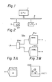
- Figure 1 shows a data processing system for explaining the background of the present invention.
- the data processing system includes a host central processing unit (CPU) 1, a main channel 2, an image memory control device 3, and an input/output unit (I/O) 4 such as a display unit.
- the image memory control device 3 includes an image memory 30 pertaining to the present invention and a printer (not shown in Fig. 1).
- the CPU 1 communicates through the main channel 2 with the image memory control device 3 or I/O unit 4. Character data of characters to be printed out from the image memory control device 3 or certain instructions for operating the image memory control device 3 are generated from the CPU 1 and are transferred through the channel 2 to the image memory control device 3.
- the image memory functions as a data buffer for transferring one page of image data to be output to a printer assembly (not shown in Fig. 1).
- the image memory 30 is a specific system which is a modification of a virtual memory as will be described later in more detail.
- Figure 2 shows an example of a conventional image memory control device.
- the conventional image memory control device includes two image memories (IMM - and IMM 2 ) 30al and 30a2, and a selector (SEL) 30a3.
- Each of the two image memories 30al and 30a2 has a capacity for storing one page of image data.
- the selector selects the second image memory 30a2 for a writing operation.
- the second image memory 30a2 is accessed for writing one page of data therein by specifying logical addresses LA corresponding to the logical address space of the second image memory 30a2.
- the selector selects the first image memory 30al for writing a next one page of image data. This constitution ensures a high speed reading operation because the image data can be continuously read without stoppage due to a write operation.
- the above-mentioned conventional device needs the two image memories, or two pages of memory capacity, resulting in the disadvantage of needing a large memory capacity.
- a single image memory having a memory capacity of one page may be provided as shown in Fig. 3A.
- a portion A indicated by slash lines represents a logical space where image data has been read so that this portion A can be used to write data
- a portion B represents a logical space from which image data has not been read. If write data is written sequentially from the top to the bottom of the logical space, the single image memory can store data simultaneously with the reading operation. However, the logical addresses of the write data are not always supplied sequentially from the top to the bottom of the logical space. Assume an example, as shown in Fig.
- image data of an X axis 1 is first written into the image memory, and then image data of Y axis 2 is written, and, finally, image data of a line 3 is written. Then, the image data of the X axis can be written into the image memory only after the reading operation is finished from the top logical address (0, 0) of the logical space to the end logical address (X, Y) of the X axis. Therefore, simultaneous writing and reading operations cannot always be carried out. In this case, the next reading operation must often be started only after writing one page of image data. As a result, a continuous reading operation cannot be effected by this single image memory.
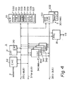
- Figure 4 is a block diagram generally showing the image memory control device 3 (Fig. 1).
- the image memory control device 3 includes the image memory 30 (Fig. 1), a control processor (CTP) 31, a channel controller (CHC) 32, a global memory (GLM) 33, an imaging hardware (IMH) 34, a print controller (PRC) 35, a control bus (C-BUS) 36, a memory bus (M-BUS) 37, and an image data bus (I-BUS) 38.
- Dash lines in Fig. 4 represent paths for transferring control signals. Solid lines represent paths for transferring data.
- the CTP 31 includes a local memory (LM) 310 consisting of a read only memory (ROM) and a random access memory (RAM) for storing a control program.
- the RAM also functions as a work area.
- the CTP 31 controls the whole of the device 3 and also carries out preprocessing for the IMH 34.
- the CTP 31 may be realized by a microprocessor.
- the CHC 32 is connected through the main channel 2 (Fig. 1) to the CPU 1 (Fig. 1), and carries out a transfer operation of character data or graphic data from the CPU 1 to the GLM 33 by a direct memory access method (DMA).
- DMA direct memory access method
- the GLM 33 includes an intermediate buffer (IB) 330, a page buffer (PB) 331, a graph data buffer (GDB) 332, an image data buffer (IDB) 333, a form overlay memory (FOM) 334, a character generating memory (CG) 335, a form control buffer (FCB) 336, and a character translation table (TT) 337, some of which are described later in more detail.
- the GLM 33 has a memory capacity in the range, for exarrple, from 0.5 megabytes to 2.5 megabytes.
- the IMH 34 is a hardware for converting code data or compacted data stored in the GLM 33 into bit pattern data, and for writing the bit pattern data into the IMM 30, under the control of the CTP 31.
- the IMH 34 includes a character generator controller (CGC) 340, a vector generator controller (VGC) 341, an overlay pattern controller (OVC) 342, and an image generator controller (IMC) 343.
- CGC character generator controller
- VCC vector generator controller
- OVC overlay pattern controller
- IMC image generator controller
- the CGC 340 is indispensable to and is always provided in the IMH 34.
- the CGC 340 has a function of imaging character codes stored in the CG 335 in the GLM 33. Each of the character codes is obtained by converting character data transferred from the CPU 1 (Fig. 1) into an internal expression, i.e., a code of four bytes per character.
- the character codes are supplied from the CG 335 in the GLM 33 through the M-BUS 37 to the CGC 340 by DMA when the CTP 31 activates the CGC 340.
- the other controllers, i.e., VGC 341, OVC 342, and IMC 342, are optionally provided.
- the VGC 341 has a function of imaging graphic data codes stored in the GDB 332 in the GLM 33.
- the data supplied to the VGC 341 are graphic codes which are obtained by converting graphic data transferred from the host CPU 1 (Fig. 1) into an internal expression.
- the VGC 341 also accesses the GDB 332 in the GLM 33 through the M-BUS 37 by DMA when the CTP 31 activates the VGC 341.
- the OVC 342 has a function of restoring compressed overlay data
- the IMC 343 has a function of restoring compressed image data.
- the C-BUS 36 is a bus which conforms with the CTP 31.
- the C-BUS 36 consists of a 24-bit address bus and a 16-bit data bus. All of the memories and registers in the image memory control device 3 can be mapped within the address space of the C-BUS 36.
- the C-BUS 36 can transfer 8-bit data or 16-bit data.
- the M-BUS 37 is a bus used only for DMA from the GLM 33 to the IMH 34, and can operate independently from the C-BUS 36.
- the M-BUS 37 consists of, for example, a 24-bit address bus and a 16-bit data bus.
- the M-BUS 37 always transfers 16-bit data.
- the IMM 30 is a memory for storing image data output from the IMH 34.
- the image data output from the IMH 34 is bit pattern data.
- the IMM 30 has specific hardware, according to an embodiment of the invention, functioning as an address conversion for realizing two pages of logical memories in spite of using only one page of a real memory.
- the IMM 30 consists, as an example, of two memory planes (IMM) 301 and 302.
- the first memory plane 301 is used for two pages of character image data developed by the CGC 340.
- the second memory plane 302 is optionally provided and is used for two pages of graphic image data developed by the VGC 341.
- the PRC 35 controls an interface between the IMM 30 and a printing assembly (not shown in Fig. 4). Synchronously with a printing process timing in the printing assembly, the PRC 35 transfers the image data from the IMM 30 to the printing assembly. When the IMM 30 consists of two memory planes, the PRC 35 should be of a larger size.
- the operation of the image memory control device 3 shown in Fig. 4 is as follows.
- the CHC 32 receives character data from the host CPU 1 (Fig. 1) and then transfers it through the M-BUS 37 to the GLM 33 by DMA.
- the CTP 31 supervises this data transfer as well as forms the contents of the PB 331 in accordance with the received character data. Once one page of contents is formed in the PB 331, the CTP 31 generates an instruction to the CGC 340 so that the CGC 340 receives the character codes from the PB 331 and develops a bit pattern of the character data.
- the IMM 301 then stores the developed bit pattern of image data. When the development of the bit pattern is finished, the CGC 340 informs the CTP 31 that the development is ended.
- the CTP 31 generates an instruction to the PRC 35-so as to read data from the IMM 301.
- the PRC 35 reads data from the IMM 301 and outputs it as video signals VS synchronously with the operation of the printing assembly.
- the next page of contents is formed in the PB 331; the CGC 340 develops a bit pattern of the next page of the character data; and the IMM 301 stores the next page of the developed bit pattern, in a manner similar to the above-mentioned operation for the first page.
- the CTP 31 activates the VGC 341 after one page of graphic data is stored in the PB 331 so that the VGC 341 develops a bit pattern of one page of the graphic data.
- the IMM 302 then receives the bit pattern of the graphic data. The simultaneous operation of reading the first page of the graphic data from the IMM 302 and storing the next page of the graphic data into the IMM 302 is similar to the operation for the character data.
- the PRC 35 takes a logical OR of the outputs from the IMMs 301 and 302.
- Figure 5A is a flow chart for explaining the data flow from the CHC 32 to the IMH 34 in the device 3 shown in Fig. 4.
- the CTP 31 receives an instruction code IC and data D from the CPU 1 through the CHC 32.
- the instruction code IC has a format shown, as an example, in Fig. 5B.
- the instruction code in this example consists of one byte, i.e., 8 bits from 0 through 7.
- the main contents of the instruction code indicate whether the data from the CPU 1 is character data CD or graphic data GD, or constitutes an instruction to access the contents of the FCB 336 (Fig.
- Fig. 5B when only the most significant bit 7 in the high order four bits is "1", the instruction code indicates that the data from the CPU 1 is character data.
- the low order four bits 0 through 3 represent a channel number CH.NO, which determines a line on a page, i.e., the vertical position of the character to be printed out on a page.
- the instruction code indicates that the data from the CPU 1 is graphic data.
- the instruction code constitutes an instruction to access the FCB 334.
- An instruction code having another bit pattern can issue an instruction to operate the printer assembly.
- the CTP 31 stores the data from the CPU 1 into the IB 330 in the GLM 33 without any modification of the received data.
- the CTP 31 analyses the instruction code IC so as to determine whether the data is character data CD or graphic data GD.
- graphic data processing is carried out by a graphic generator including the GDB 332, the VGC 341, and the IMM 302.
- the vertical position of the character to be printed out on a line of one page is determined with reference to the FCB 334 based on the received instruction code.
- the format of the FCB 334 is shown as an example in Fig. 5C.
- the contents of the FCB 334 are previously determined in accordance with the desired printing format. Assume that the length of one page 50 is 12 inches, and that the minimum line pitch between adjacent lines is 12 lines/inch. Then the maximum line number on one page is 144 lines, 0 through 143. Accordingly, the FCB 334, which determines the vertical position of each line on the page, consists, at maximum, of 144 columns,"0" through "143", each column corre- spondin g to one line on the page 50. Each column in the FCB 334 consists of a line pitch control data LP indicating the line pitch and a channel number CH.NO. indicating a line to be skipped.
- the channel number CH.NO is one of "0" through “12".
- the same channel numbers may be provided in different columns in accordance with the desired printing format.
- the CTP 31 counts up the number of times the same channel numbers are received. For example, when the instruction code specified at first the channel number "1" in the FCB 334 shown in Fig. 5C, the CTP 31 searches, starting from the column “0", the first "1" of the channel number. Since the first channel number "1" is stored in the column "3" in this example, the CTP 31 moves its pointer to control the line "3". Then, assume that the instruction code specifies the channel number "1" again, the CTP 31 searches the second "1" of the channel number. The second channel number "1" is stored in the column "5".
- the CTP 31 skips its pointer from the column “3" to the column "5". If the next instruction code specifies the channel number "7", the CTP 31 moves its pointer from the column "5" to the column "143” if the columns "0" through “142" do not store the channel number "7".
- the line pitch LP is one of "0", "1", and "2", which respectively represent that the pitch between adjacent lines are 6 lines/inch, 8 lines/inch, and 12 lines/inch. Assume that the resolution of the printer is 240 dots/inch. Then the character data on the first line "0”, if specified by the instruction code,is developed at the position vertically lower by 40 dots from the top of the page, because the first column "0" contains the line pitch "0", i.e., 6 lines/inch, and therefore, one line needs 40'dots in the vertical direction.
- the character data on the second line "1" if specified by the instruction code, is developed at the position vertically lower by 30 dots from the first line "0", because the second column "1" contains the line pitch "1", i.e., 8 lines/inch, and therefore, one line needs 30 dots in the vertical direction.
- the CTP 31 reads the character data byte by byte from the IB 330 in the GLM 33.
- the read data is processed as a hexadecimal Extended Binary-Coded Decimal Interchange Code (EBCDIC) of a character code. That is, at step 506, the read character code is translated into a top address of the character pattern stored in the CG 335 of the GLM 33, with reference to the character translation table (TT) 337 in the GLM 33.
- EBCDIC Extended Binary-Coded Decimal Interchange Code
- the TT consists of 256 columns. Each column stores the top address of a character pattern corresponding to the character code (EBCDIC).
- the CG 365 stores character patterns for characters A, B, C, ....
- the identified top address a tl is stored at step 507, in the PB 331.
- the top address TA a t2 of the character B is identified and stored, at step 507, in the PB 331.
- Figure 5E shows the format of the page buffer (PB) 331.
- PB page buffer
- FIG. 5E other than the above-mentioned top addresses TA of the character patterns, movement amounts MA in the horizontal direction and addresses PMDA for accessing a printing-data memory (see Fig. 6) in the CGC 371 are also stored, at step 507, in the PB 331.
- the printing-data memory will be described later in more detail.
- the movement amounts MA are explained with reference to Fig. 5F.
- the movement amounts are the distances from the print start positions of characters on a page in the horizontal direction.
- the print start position for each line on a page is stored in the printing-data memory.
- the movement amount for the character "A” is "0"
- the movement amount for the character "B” is "S 1 "
- the movement amount for the character "C” is "S 2 ".
- S 1 is 24
- S 2 is 48.
- the CTP 31 sets, at step 509, an end flag EF in the PB 331.
- the PB 331 stores the character information for all characters to be printed on one page, including the movement amounts MA, the top addresses TA of the character patterns, and the addresses PMDA for accessing the printing-data memory.
- the CTP 31 sets the necessary parameters in the CGC 340. These parameters are necessary for developing the character data into a bit pattern data.
- the CTP 31 requests the CGC 340 to develop the character data into bit pattern data.
- the CGC 340 then starts to operate.
- FIG. 6 shows a block diagram of the CGC 340 in the device 3 shown in Fig. 4.
- the CGC 340 includes the printing-data memory (PDM) 61 as mentioned before, a control register 62, a CGC controller (CONT) 63, a CG access circuit (ACS) 64, and a write circuit (WC) 65.
- PDM printing-data memory
- CONT CGC controller
- ACS CG access circuit
- WC write circuit
- the PDM 61 and the control register 62 store necessary parameters as described before with reference to Figs. 5A and 5E, and in particular, at step 510 in Fig. 5A. More specifically, the PDM 61 stores starting addresses of respective lines to be printed on one page, and a plurality of character parameters including a flag indicating whether the character to be printed should be rotated or not, a width, and a height, for each character.
- the control register 62 includes a command register (C.REG) 621 for storing a start ccmmand for starting the operation of the CGC 340, a status register (S.REG) 622 for storing status data of the CGC 340, a memory address register (MA.REG) 623 for indicating a top address TA in the PB 331, and a line address register (L.REG) 624 for storing a vertical position (see FCB in Fig. 5C) of the character to be printed.
- C.REG command register
- S.REG status register
- MA.REG memory address register
- L.REG line address register
- the CTP 31 After the CTP 31 sets the contents of the PB 331, provides the data in the PDM 61, sets the top address of the PB 331 in the M.A. REG 623, and sets the vertical position in the L.REG 624, then the CTP 31 writes a start command into the command register 621.
- the CONT 63 In response to the start command from the command register 621, the CONT 63 starts to operate as follows:
- the CONT 63 calculates the position of the character to be written, based on the data of the starting address of a line stored in the PDM 61 and the movement amount MA included in the data read from the PB 331.
- the CONT 63 reads the corresponding character parameters from the PDM 61, and transfers the read character parameters to the WC 65.
- the CONT 63 activates the WC 65 to start its operation.
- the above operation is sequentially repeated until the end flag EF is read from the PB 331 to the CONT 63.
- the CONT 63 informs the CTP 31 (Fig. 4) through the status register 622 that the writing operation for one page is finished.
- Figure 7 shows in detail the write circuit (WC) 65 included in the CGC shown in Fig. 6.
- the WC 65 includes a parallel-serial converting shift register (SRa) 650, a serial-parallel converting shift register (SRb) 651, an X counter 652, a Y counter 653, an H counter 654, a V counter 655, a write control circuit (WCC) 656, and a multiplexer 657.
- SRa parallel-serial converting shift register
- SRb serial-parallel converting shift register
- X counter 652 X counter
- Y counter 653 a serial-parallel converting shift register
- H counter 654 a serial-parallel converting shift register
- V counter 655 a write control circuit
- WCC write control circuit
- the X counter 652 is a counter for supervising the X addresses of the IMM 301;
- the Y counter 653 is a counter for supervising the Y addresses of the IMM 301;
- the H counter 654 is a counter for supervising the width of a character;
- the V counter 655 is a counter for supervising the height of a character.
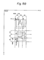
- Figure 8A is a flow chart for explaining the operation of the WC 656 shown in Fig. 7.
- Fig. 8A and in the following description of the operation of the WC 656, a horizontal accessing process is mainly described.
- all vertical accessing processes are placed within parentheses. The operation is carried out in the following sequence.
- step 808 is executed.
- the reason why the two shift registers SRa 650 and SRb 651 are provided in the WC 65 will be understood with reference to Fig. 8B, in which write positions on the logical space of the IMM 301 are illustrated for both the lateral access and the vertical access.
- the width H of the character A is illustrated as 32 bits.
- the SRa 650 at first receives 16 bits from the CG 335, as indicated by slash lines.
- the top address of the character pattern A is (X I Y,) for the lateral access or (X 2 , Y 2 ) for the vertical access. As shown in Fig. 8, the X address X 1 or the Y address Y 2 does not always coincide with the most significant bit MSB of the 16 bits.
- the X address X 1 or the Y address Y 2 is spaced from the MSB by 6 bits. Since the WCC 656 knows the X address X l or the Y address Y 2 , the SRb 651 does not store the high order 6 bits, and only the remaining 10 bits are sequentially shifted into the SRb 651, from the higher order bit, i.e., bit 9, to the lower order bit, i.e., bit 0. Thus, the SRb 651 outputs only 10 bits at the first writing operation. Since the high order 6 bits in the received 16 bits are neglected, the operating speed is increased. In the second writing operation, all 16 bits are shifted from the SRa 650 to the SRb 651. In the third writing operation, however, only the high order 6 bits in the received 16 bits are shifted into the SRb 651.
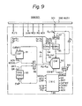
- FIG. 9 is a block circuit diagram showing the image memory 301 according to an embodiment of the present invention.
- the IMM 301 is connected to the I-BUS 38 which is used only for accessing the IMM 301 or IMM 302 (Fig. 4).
- the IMM 301 includes a cell address translate table (CAT) 91, a cell memory (CM) 92, a cell address queue (CAQ) 93, a first address translate circuit (EORa) 94, a second address translate circuit (EORb) 95, a first multiplexer (MPXa) 96, a second multiplexer (MPXb) 97, a third multiplexer (MPXc) 98, and an image memory control circuit (IMC) 99.
- CAT cell address translate table
- CM cell memory
- CAQ cell address queue
- EORa first address translate circuit
- EORb second address translate circuit
- IMC image memory control circuit
- the CAT 91 is a logical memory for storing a table which is used to translate a logical address into a real address.
- the CM 92 is a real memory for storing bit image data.
- the CAQ 93 is a "first-in first-out” (FIFO) circuit for supervising real memory cells which are not being used.
- the EORa 94 and the EORb 95 are circuits for translating addresses and data sequences so as to realize lateral access, vertical access, or plane access.
- X 0 through X 11 , and Y 0 through Y 11 represent address lines for specifying a read or write logical address of the IMM 301 from the IMH 34 (Fig. 4).
- P represents an address line for specifying a page used for reading or writing.
- DO through D 15 are data lines for reading from or writing in data by the IMH 34.
- R/W is a signal for discriminating whether data is read from or data is written in the IMM by the IMH 34.
- RQ is an access request signal from the IMH 34.
- ACK is an access permission signal from the IMM 301 to the IMH 34.
- the logical space LS in this example has only nine logical cells LC each having an address space of 64 bits x 64 bits.
- Each logical cell is a unit of a virtual memory:
- the CM 92 has nine real cells RC each having the same address space of 64 bits x 64 bits as that of the logical cell LC.
- the logical cells LC and the real cells RC may relate to each other in one to one correspondence.
- the NOCELL bit indicates whether or not correspondence is established between the logical cell and a real cell.
- the logical cell having the logical address 00 corresponds to the real cell having the logical address 00;
- the logical cell 01 corresponds to the real cell 01;
- the logical cell 10 corresponds to the real cell 02; and
- the logical cell 11 corresponds to the real cell 04.
- the NOCELL bits in the columns 00, 01, 10, and 11 are labelled "1".
- the CAQ 93 is an FIFO having nine columns. Each column stores a real address of a real cell which can be used to write data therein or to read data therefrom, i.e., which is not in use.
- the direction of data flow in the CAQ 93 is from the bottom to the top, as indicated in the figure by an arrow. Empty columns in the CAQ 93 mean that any real address except for the real addresses stored in the CAQ 93 may be made to correspond to a logical address.
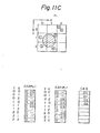
- Figure 11A shows the initial states of two CATs, i.e., CAT (P O ) for the first page and CAT (P 1 ) for the second page, and the CAQ.
- the CAQ stores all of the real cell addresses 00 through 08. Therefore, all of the real cells can be used for the write operation.
- NOCELL bits in the CAT (P O ) and CAT (P 1 ) are all "0" indicating that no logical cell corresponds to any one of the real cells, even when each column in the CAT (P O ) and CAT (P 1 ) stores any real address.
- the CAT (P O ) stores the real addresses 00, 01, 02, and 03 in the columns 00, 01, 10 and 11, respectively. Simultaneously with the storing operation, the NOCELL bits in these columns 00, 01, 10, and 11 are turned to "1". In this state, the columns 02, 12, 20, 21 and 22 of the CAT (P O ) and all columns of the CAT (P 1 ) are free to store any real address.
- the CAQ stores the real addresses 04, 05, 06, 07 and 08 which are free to be used.
- the read real cell After reading the image data, the read real cell is opened to be used by changing the NOCELL bit in the CAT 91. Therefore, during the reading of one page, simultaneous writing in another page is possible. As a result, a continuous reading operation from the first page to the second page becomes possible.
- the writing of image data in the logical space is not limited to a from top to bottom operation.
- a circle is written in a lower portion of the logical space, and then a rectangular is written in a upper portion of the logical space.
- Figure 12 is a flow chart for explaining the operation of the image memory shown in Fig. 9.
- the logical address for accessing the CAT 91 is determined by the data X 6 through X 11' Y 6 through Y 11 , and P.
- the low order six bits X o through X 5 and Y O through Y are not taken into account in the description with reference to Fig. 12 because one logical cell consists of 64 bits x 64 bits.
- the data P represents the page P 0 or P 1 .
- the CAT 91 is accessed so that the AOV bit and the NOCELL bit corresponding to the logical address are read.
- the IMC 99 discriminates whether the AOV bit is "1" or "0".
- the determined address is an inhibited area for writing. Therefore, if the IMC 99 discriminates, at step 1203, that the R/W signal from the I-BUS 38 is a write signal, no process is carried out. If the R/W signal is a read signal, then, at step 1204, the IMC 99 outputs "0" which is transferred through the multiplexers 98, 97, EORb 95, data bus DO through D 15 , and the I-BUS 38, to the PRC 35, so that a white space is printed.
- IMC 99 discriminates the NOCELL bit. If the NOCELL bit is "0", this logical address can be allocated to a real address. If, at step 1206, the R/W signal is the read signal, a white space is printed at step 1204 because the real cell allocated to this logical address has been read and is not in use as the NOCELL bit is "0". If the R/W signal is the write signal, however, then, at step 1207, the IMC 99 discriminates whether or not CAQ 93 is empty by a signal EMP from the CAQ 93. If the CAQ 93 is empty, no real cell can be used so that, at step 1208, the IMC 99 sets the REJ to "1". The reject signal REJ is transferred through the I-BUS 38 to the IMH 34. In response to the reject signal REJ of "1", the IMH 34 again accesses the IMM 301.
- the IMC 99 If the CAQ 93 stores at least one real cell at step 1207, then, at step 1209, the IMC 99 generates a read signal QR so that the real address is read from the CAQ 93.
- the IMC 99 generates a write signal CATWT so that the taken out real address is stored in the logical address of the CAT 91. Simultaneously, the NOCELL bit in this logical address is turned to "1".
- the IMC 99 generates a write signal CMWT so that, by the specified logical address, data from the IMH 34 through the I-BUS and data bus DO through D 15 is written into the real cell which is allocated to the specified logical address.
- step 1205 If the NOCELL bit is "1" at step 1205, this means that a real cell has been allocated to the specified logical address. Therefore, at step 1212, the real address allocated to the specified logical address is read from the CAT 91.
- step 1213 if the R/W signal is the write signal, step 1211 is carried out. If the R/W signal is the read signal, then, at step 1214, data is read from the real address of the C M 92. The read data is transferred through the data bus D 0 through D15 and the I-BUS 38 to the PRC 35.
- the IMC 99 discriminates whether or not a DUMP signal is transferred from the PRC 35.
- the DUMP signal is generated after each real cell is read.
- the DUMP signal signifies, in lateral accessing, that the data in one real cell having 64 horizontal lines (Y 0 - Y 5 ) is completely read.
- the DUMP signal also signifies, in vertical accessing, that the data in one real cell having 64 vertical lines (X 0 - X 5 ) is completely read. If the DUMP signal is not received, the process goes to END. If the DUMP signal is received, the IMC 99 generates a write signal CAWT so that the real address of the real cell read at the step 1214 is written into the CAQ 93. Then, at step 1217, the NOCELL bit in the specified logic address of the CAT 91 is turned to "0".
- Figure 13 is a logic circuit diagram of the IMC 99 in the IMM 301 shown in Fig. 9.
- the IMC 99 includes OR gates 131 and 136, and AND gates 132 through 135 and 137 and 138.
- the IMC 99 receives the signals NOCELL, AOV, R/W, DUM, and EMP, and outputs the signals BLNK, QR, QWT, CATWT, CMWT, and REJ.
- the OR gate 131 and the AND gate 132 carry out the process of the steps 1203 through 1208 in the flow chart shown in Fig. 12.
- the AND gates 133 through 136 carry out the steps 1209 through 1211 and the steps 1215 through 1217.
- the AND gates 137 and 138 carry out the steps 1202, 1203, 1206, and 1207.
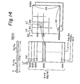
- FIG 14 shows the structure of the CAT 91 in the IMM 301 shown in Fig. 9.
- each logical address LOG.ADD of the CAT 91 consists of P , Y 11 through Y 6 , and X 11 through 1 6 .
- the total number of bits in each logical address is thus 13.
- a DD corresponds to one logical cell LC in the logical space LS.
- Each logical cell LC consists of 64 bits x 64 bits.
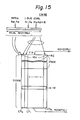
- FIG. 15 shows the structure of the CM 92 in the IMM 301 shown in Fig. 9.
- each real address of the CM 92 consists of 19 bits, i.e., A3 through A O from the EORa 94, A 7 through A4 from the I-BUS 38, and A 18 through A 8 from the CAT 91 through the MPXa 96.
- the low order bits of the logical addresses or real addresses are not taken into account.
- the low order bits are used in order to develop the image data into a bit pattern on the CM 91, and, in particular, in order to realize the lateral accessing or vertical accessing, as later described in more detail.
- the logical space for one page consists of 4 K cells as described with reference to Fig. 14. The reason why the number of real cells is smaller than the number of logical cells is because the size of the printing page does not always require the same address space as the logical space. For example, when the printing paper has different longitudinal and horizontal side lengths, the real address space does not require the full square of the longer side.
- the high order address signals A 18 through A are obtained by address conversion from the address signals X 6 through X 11 , Y 6 through Y 11 , and P by the CAT 91 and the CAQ 93, as described before with reference to Figs. 10 through 12.
- the middle order address signals A 7 through A4 are directly obtained from the address signals X 4 , X 5 , Y 4 , and Y 5 . These addresses are commonly specified for all of the memory chips CP O through CP 15 .
- the low order addresses A3 through A 0 are different for respective memory chips CP 0 through CP 15 .
- These addresses A3 through A O are obtained by converting the addresses X 3 through X o , and Y 3 through Y 0 by the EORa 94, as later described in detail. This conversion is necessary in order to carry out lateral accessing, vertical accessing, or plane accessing.
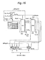
- FIG. 16 is a block diagram showing in detail the EORa 94 and the EORe 95 in the IMM 301 shown in Fig. 9.
- the EORa 94 includes a multiplexer 161 and an address arranging circuit (AR) 162.
- the EORb 95 includes an address rearranging circuit (RAR) 163, and sixteen multiplexers 164-1 through 164-16.
- the multiplexer 161 receives the address signals X 0 through X 3 , Y 0 through Y 3 , and a function signal FUNK indicating whether the access to the CM is a vertical access (1 bit x 16 bits), horizontal access (16 bits x 1 bit), or plane access (4 bits x 4 bits). In response to the function signal FUNK, the multiplexer selects output signal R 0 through R 3 .
- the relationship between the function signal FUNK and the output signals R 0 through R 3 is shown in a table in Fig. 16. That is, when the function signal FUNK is 00, indicating that vertical accessing should be carried out, then the multiplexer 161 selects the address signals X 0 through X 3 as the output signals R 0 through R 3 .
- the multiplexer 161 selects the address signals X 0 , X 1 , Y 0 , and Y 1 as the output signals R 0 through R 3 .
- the multiplexer 161 selects the Y 0 through Y 3 as the R 0 through R 3 .
- the R 0 through R 3 are supplied to the AR 162 and to the RAR 163.
- the AR 162 generates, in accordance with a predetermined rule and in response to the FUNK, sixteen addresses as the low order addresses (A O through A 3 ) x 16 for accessing respective memory chips CP 0 through CP 15 .
- the sixteen addresses (A O through A 3 ) x 16 differ from each other, as mentioned with reference to Fig. 15.
- the low order addresses (A O through A3) x 16 are determined for the vertical, lateral, or plane accessing.
- the RAR To write data in or to read data from the CM 92, the RAR generates, in accordance with an another predetermined rule and in response to the FUNK, sixteen data selecting signals. Each of the data selecting signals consists of four bits. These data selecting signals are applied to the multiplexers 164-1 through 164-16 respectively. Thus, the multiplexers 164-1 through 164-16 respectively select corresponding data transferred from the MPXb 97 (Fig. 9), as data to be output. The data output from the multiplexers 164-1 through 164-16 is then transferred to the CM 92 to be written therein or to the I-BUS 38 as read data.
- the addresses of 16 bits for one accessing always construct one word from sixteen memory chips CP O through CP 15 .
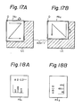
- Figure 17A is a diagram for explaining a feeding direction of a printing paper PA 1 , for printing a so-called portrait style.
- Figure 17B is a diagram for explaining another feeding direction of a printing paper PA 2 , for printing a so-called landscape style.
- the printing papers PA1 and PA 2 often have different longitudinal and horizontal side lengths.
- the feeding direction in both cases is usually perpendicular to the shorter side of the printing paper because of the drum size of the printer assembly.
- the characters and pictures are printed in the direction parallel to the shorter side of the printing paper PA 1 , as shown in Fig. 18A.
- the characters and pictures are printed in the direction parallel to the longer side of the printing paper PA 2 , as shown in Fig.18B.
- the logical space LC is shown as a square.
- the RPC 35 (Fig. 4) reads the CM 92 (Fig. 9) in the direction perpendicular to the paper feeding direction.
- FIG. 19 is a block diagram showing the general constitution of the PRC 35 shown in Fig. 4.
- the PRC 35 includes an IMM interface control circuit (INT CONT) 191, an address control circuit 192, a mode control circuit (MOD CONT) 193, a video control AND gate 194, a shift register (SR) 195, and a data buffer register (DBR) 196.
- IMM interface control circuit INT CONT
- address control circuit 192
- MOD CONT mode control circuit
- SR shift register
- DBR data buffer register
- the PRC 35 sends various control signals from the INT CONT 191, the ADD CONT 192, and the MOD CONT 193 through the I-BUS 38 to the IMM 30 (Fig.-4).
- the DBR 196 receives image data (IMD) from the IMM 30 through the I-BUS 38.
- the data once stored in the DBR 196 is transferred to the SR 195.
- the SR 195 then converts the image data into serial data in accordance with a control signal from the INT CONT 191.
- the serial data from the SR 195 is gated by the AND gate 194.
- the video signal VS is obtained as a logical product of the serial data and a video control signal (VCS) from the INT CONT 191.
- VCS video control signal
- the INT CONT 191 sends the dump signal DUM when the PRC has read one real cell, so as to open the real cell, i.e., to allow it to be used for writing new data therein.
- the MOD CONT 193 controls the reading direction, i.e., the portrait or the landscape by generating a mode signal MOD.
- the ADD CONT 192 controls the reading address.
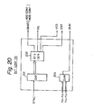
- Figure 20 shows the constitution of the INT CONT 191.
- a line address counter (CNT) 201 counts one scanning line (64 counts).
- a signal generator (SIG GEN) 202 Based on the counting value, a signal generator (SIG GEN) 202 generates a timing data IBACC for transferring address signals and mode data, the timing data being supplied to the ADD CONT 192 and MOD CONT 193 (Fig. 19), the data request signal REQ, the video control signal VCS, and the data set timing signal DST being applied to the DBR 196 and the SR 195 (Fig. 19).
- a dump instructing circuit (DUM) 203 generates the dump signal DUM based on the addresses X o through X 5 and Y 0 through Y 5 for accessing the IMM 30.
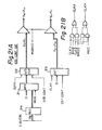
- Figure 21A shows the constitution of the address control circuit (ADD CONT) 192 shown in Fig. 19.
- AD CONT address control circuit
- a count value "0" is initially loaded from a multiplexer 211 into an up/down counter 212 for generating the X addresses X 0 through X 11 .
- an up/down control signal U/D CONT controls the U/D CNT 211 so as to count up by sixteen in response to one clock signal CLK-X which represent a data set timing (CLK 1).
- a value representing the width in the X direction of the printing paper is loaded from a register (REG) 214 into the U/D CNT 212 for generating the X addresses.
- the value is transferred from the C-BUS 36 and is previously stored in the register 214.
- Figure 21B shows a logic circuit for generating the clock signals CLK X and CLK Y.
- MOD when the portrait style printout takes place, MOD is "1” and * MOD is “0” so that the CLK X is equal to the CLK 1 and the CLK Y is equal to the CLK 2.
- * MOD is "1” and MOD is "0” so that the CLK X is equal to the CLK 2
- the CLK Y is equal to the CLK 1.
- the explanation of the IMM 30 is mainly described with respect to the character generator controller (CGC) 340, the principal idea of the allocation of the real cells to logical addresses in an embodiment of the invention can be similarly applied when the vector generator controller (VGC) 341, the overlay pattern controller (OVC) 342, or the image generator controller (IMC) 343 is activated.
- VCC vector generator controller
- OFC overlay pattern controller
- IMC image generator controller
- the unit of the real cell or logical cell is not restricted to the described example of 64 bits x 64 bits, but may be of any scale including 1 bit x 1 bit.
- the CAQ 93 is described as a "first-in first-out" (FIFO) circuit.
- any memory can be used for storing the real addresses which are not being used as long as its input sequence and output sequence are controlled under a certain acknowledgeable condition.
- a memory access control apparatus in which a single image memory plane can be used for simultaneous reading and writing of different pages even when writing is effected out of sequence.
- an embodiment of the invention can provide an improved memory access control apparatus in which the real memory storing capacity is decreased without reducing the reading speed.
- a memory access control apparatus in an embodiment of this invention can effect a continuous reading of different pages on the logical space without employing different real memory planes but using a single real memory plane.
- the writing of image data in one page of a logical space is not limited to a from top to bottom operation but the image data can be written in any position on the page as long as at least one real cell is not being used for reading or writing.
- embodiments of this invention may be particularly advantageous in the field of high speed transmission of image data from an image memory to, for example, a laser printer.
Abstract
Description
- The present invention relates to memory access control apparatus.
- A related art is discussed in Japanese Patent Application No. 58-117405, filed on June 29, 1984, in which a laser printer, for example, is required to continuously print out image data at a high speed, and therefore, a higher speed transmission of image data from an image memory to the laser printer is necessary.
- In order to continuously read image data, two image memories may be provided. Here, while one of the image memories is storing one page of image data, another one page of image data is read from the other image memory. This constitution, however, requires two image memories for simultaneously storing and reading two pages of image data, with the result that memory capacity as a whole must be made large.
- It is possible to provide an image memory having a capacity for storing just one page of image data, and new image data may be sequentially written into an area from which the previous image data has been read. This constitution, however, cannot provide a high reading speed when the written image data is not written in sequence from the top to the bottom of the page, as later described in more detail with reference to the drawings.
- Accordingly, it is desirable to provide a memory access control apparatus which requires less memory storing capacity, without deteriorating the reading speed.
- There is provided, according to one aspect of the present invention, a memory access control apparatus comprising:
- a memory having a memory capacity of a plurality of transfer units of data;
- a writing means for writing data into said memory in a logical address sequence different from a reading logical address sequence effected for reading said data from said memory;
- a reading means for reading data from said memory in a logical address sequence different from a logical address writing sequence effected for writing said data into said memory;
- an address detecting means for detecting a real address at which the read data has been stored in said memory;
- a correspondence storing means for storing a correspondence between a real address at which a transfer unit of data is being stored in said memory and the corresponding logical address used to write said transfer unit of data; and
- a control means for controlling said writing means so as to write, at a read real address detected by said address detecting means, next transfer unit of data, after said transfer unit of data previously stored at said read real address has been read, by specifying said corresponding logical address stored in said correspondence storing means.
- The memory may have a real address space to cover within one page of a printing paper, and the correspondence storing means a logical space to cover at least two pages of the printing papers.
- The correspondence storing means preferably comprises, at each logical address, a correspondence establishing bit indicating whether or not the correspondence is established. The correspondence establishing bit is turned on after the transfer unit of data is written into the memory. The correspondence establishing bit is turned off after the transfer unit of data is read. A new real address is made to correspond to the logical address at which the correspondence establishing bit is turned off.
- The address detecting means may be a first-in first-out circuit for storing the read real address after the transfer unit of data is read from the real address and for outputting the read real address, the output read real address being made to correspond to a specified logical address at which the correspondence establishing bit is turned off.
- The correspondence storing means preferably comprises, at each logical address, a correspondence inhibiting bit indicating whether or not the logical address is permitted to correspond to a real address.
- The control means preferably comprises a blank signal generating means for generating a white area data so as to print out a white space when the correspondence inhibiting bit is in an ON state during a reading operation, or when the correspondence establishing bit is in an OFF state during a reading operation.
- The writing means and the reading means preferably further comprise an address conversion means for converting the write address or the read address into a lateral accessing address or a vertical accessing address.
- Such a memory access control apparatus can be constructed so as to be capable of high speed processing and employing an improved virtual memory system, adapted to output data from a memory to a printer such as a laser printer.
- For a better understanding of the present invention, and to show how the same may be carried into effect, reference will now be made, by way of example, to the accompanying drawings, in which:-
- Fig. 1 is a block diagram generally showing a data processing system for explaining the background of the present invention;
- Fig. 2 shows a block diagram of an example of a conventional image memory control device;
- Figs. 3A and 3B shows a logical space of an image memory and an example of a picture to be printed out, for explaining a conventional problem;
- Fig. 4 is a block diagram generally showing an image memory control device to be adapted to the present invention;
- Fig. 5A is a flow chart for explaining a data flow from a channel controller (CHC) to imaging hardware (IMH) in the device shown in Fig. 4;
- Fig. 5B shows a data format of an instruction code transferred from a central processing unit (CPU) shown in Fig. 1 to a control processor (CTP) shown in Fig. 4;
- Fig. 5C shows a data format in a form-control buffer (FCB) shown in Fig. 4;
- Fig. 5D shows a process of the translation of a character code into the corresponding top address of the character;
- Fig. 5E shows a data format in a page buffer (PB) shown in Fig. 4;
- Fig. 5F diagramatically shows a start position of each character;
- Fig. 6 is a block diagram showing in detail a character generator controller (CGC) shown in Fig. 4;
- Fig. 7 is a block diagram showing in detail a write circuit (WC) shown in Fig. 6;
- Fig. 8A is a flow chart for explaining the write control operation;
- Fig. 8B is a diagram for explaining a lateral access and a vertical access in the write control operation shown in Fig. 8A;
- Fig. 9 is a block circuit diagram showing an image memory according to an embodiment of the present invention;
- Fig. 1C shows states of a cell address translate table (CAT), a cell memory (CM), and a cell address queue (CAQ), which are included in the image memory, and also shows a state of a logical memory corresponding to the state of the CAT;
- Fig. 11A shows initial states of the two CATs and the CAQ;
- Fig. 11B shows transitional states of the two CATs and the CAQ when new data is written in one page of the logical memory;
- Fig. 11C shows transitional states of the two CATs, the CAQ, and the logical memory, when another new data is written in another page of the logical memory;
- Fig. 12 is a flow chart for explaining the operation of the image memory shown in Fig. 9;
- Fig. 13 is a logic circuit diagram of an image memory control unit in the image memory shown in Fig. 9;
- Fig. 14 shows the structure of the cell address translate table (CAT) in the image memory shown in Fig.9;
- - Fig. 15 shows the structure of the cell memory (CM) in the image memory shown in Fig. 9;
- Fig. 16 is a block diagram showing an EOR a and EORb in the image memory shown in Fig. 9, for explaining a vertical accessing and a horizontal accessing;
- Fig. 17 is a diagram for explaining an inhibit area to write for both vertical printing and horizontal printing;
- Figs. 17A and B are diagrams illustrating different feeding directions of printing paper;
- Figs. 18A and B show the arrangement of character on the paper of Figure 17A and B respectively;
- Fig. 19 is a block diagram of the print controller in Fig. 4;
- Fig. 20 is a diagram showing one form of the interface control circuit of Fig. 19;
- Fig. 21A shows one form of the address control circuit of Fig. 19; and
- Fig. 21B shows a logic circuit for generating clock signals.
- Figure 1 shows a data processing system for explaining the background of the present invention.
- In Fig. 1, the data processing system includes a host central processing unit (CPU) 1, a
main channel 2, an imagememory control device 3, and an input/output unit (I/O) 4 such as a display unit. The imagememory control device 3 includes animage memory 30 pertaining to the present invention and a printer (not shown in Fig. 1). TheCPU 1 communicates through themain channel 2 with the imagememory control device 3 or I/O unit 4. Character data of characters to be printed out from the imagememory control device 3 or certain instructions for operating the imagememory control device 3 are generated from theCPU 1 and are transferred through thechannel 2 to the imagememory control device 3. - The image memory functions as a data buffer for transferring one page of image data to be output to a printer assembly (not shown in Fig. 1). The
image memory 30 is a specific system which is a modification of a virtual memory as will be described later in more detail. - Figure 2 shows an example of a conventional image memory control device. In Fig. 2, the conventional image memory control device includes two image memories (IMM- and IMM2) 30al and 30a2, and a selector (SEL) 30a3. Each of the two image memories 30al and 30a2 has a capacity for storing one page of image data. During reading of onepage of image data from the first image memory 30al to a laser printer, for example, the selector selects the second image memory 30a2 for a writing operation. In the writing operation, the second image memory 30a2 is accessed for writing one page of data therein by specifying logical addresses LA corresponding to the logical address space of the second image memory 30a2. Similarly, during reading operation of the second image memory 30a2, the selector selects the first image memory 30al for writing a next one page of image data. This constitution ensures a high speed reading operation because the image data can be continuously read without stoppage due to a write operation.
- The above-mentioned conventional device, however, needs the two image memories, or two pages of memory capacity, resulting in the disadvantage of needing a large memory capacity.
- In order to reduce the memory capacity, a single image memory having a memory capacity of one page may be provided as shown in Fig. 3A. In Fig. 3A, a portion A indicated by slash lines represents a logical space where image data has been read so that this portion A can be used to write data, and a portion B represents a logical space from which image data has not been read. If write data is written sequentially from the top to the bottom of the logical space, the single image memory can store data simultaneously with the reading operation. However, the logical addresses of the write data are not always supplied sequentially from the top to the bottom of the logical space. Assume an example, as shown in Fig. 3B, wherein image data of an
X axis ① is first written into the image memory, and then image data ofY axis ② is written, and, finally, image data of aline ③ is written. Then, the image data of the X axis can be written into the image memory only after the reading operation is finished from the top logical address (0, 0) of the logical space to the end logical address (X, Y) of the X axis. Therefore, simultaneous writing and reading operations cannot always be carried out. In this case, the next reading operation must often be started only after writing one page of image data. As a result, a continuous reading operation cannot be effected by this single image memory. - Figure 4 is a block diagram generally showing the image memory control device 3 (Fig. 1).
- In Fig. 4, the image
memory control device 3 includes the image memory 30 (Fig. 1), a control processor (CTP) 31, a channel controller (CHC) 32, a global memory (GLM) 33, an imaging hardware (IMH) 34, a print controller (PRC) 35, a control bus (C-BUS) 36, a memory bus (M-BUS) 37, and an image data bus (I-BUS) 38. Dash lines in Fig. 4 represent paths for transferring control signals. Solid lines represent paths for transferring data. - The
CTP 31 includes a local memory (LM) 310 consisting of a read only memory (ROM) and a random access memory (RAM) for storing a control program. The RAM also functions as a work area. TheCTP 31 controls the whole of thedevice 3 and also carries out preprocessing for theIMH 34. TheCTP 31 may be realized by a microprocessor. - The
CHC 32 is connected through the main channel 2 (Fig. 1) to the CPU 1 (Fig. 1), and carries out a transfer operation of character data or graphic data from theCPU 1 to theGLM 33 by a direct memory access method (DMA). - The
GLM 33 includes an intermediate buffer (IB) 330, a page buffer (PB) 331, a graph data buffer (GDB) 332, an image data buffer (IDB) 333, a form overlay memory (FOM) 334, a character generating memory (CG) 335, a form control buffer (FCB) 336, and a character translation table (TT) 337, some of which are described later in more detail. TheGLM 33 has a memory capacity in the range, for exarrple, from 0.5 megabytes to 2.5 megabytes. - The
IMH 34 is a hardware for converting code data or compacted data stored in theGLM 33 into bit pattern data, and for writing the bit pattern data into theIMM 30, under the control of theCTP 31. TheIMH 34 includes a character generator controller (CGC) 340, a vector generator controller (VGC) 341, an overlay pattern controller (OVC) 342, and an image generator controller (IMC) 343. - The
CGC 340 is indispensable to and is always provided in theIMH 34. TheCGC 340 has a function of imaging character codes stored in theCG 335 in theGLM 33. Each of the character codes is obtained by converting character data transferred from the CPU 1 (Fig. 1) into an internal expression, i.e., a code of four bytes per character. The character codes are supplied from theCG 335 in theGLM 33 through the M-BUS 37 to theCGC 340 by DMA when theCTP 31 activates theCGC 340. The other controllers, i.e.,VGC 341,OVC 342, andIMC 342, are optionally provided. - The
VGC 341 has a function of imaging graphic data codes stored in theGDB 332 in theGLM 33. The data supplied to theVGC 341 are graphic codes which are obtained by converting graphic data transferred from the host CPU 1 (Fig. 1) into an internal expression. TheVGC 341 also accesses theGDB 332 in theGLM 33 through the M-BUS 37 by DMA when theCTP 31 activates theVGC 341. - The
OVC 342 has a function of restoring compressed overlay data, and the IMC 343 has a function of restoring compressed image data. - The C-BUS 36 is a bus which conforms with the
CTP 31. As an example, the C-BUS 36 consists of a 24-bit address bus and a 16-bit data bus. All of the memories and registers in the imagememory control device 3 can be mapped within the address space of the C-BUS 36. The C-BUS 36 can transfer 8-bit data or 16-bit data. - The M-BUS 37 is a bus used only for DMA from the
GLM 33 to theIMH 34, and can operate independently from the C-BUS 36. The M-BUS 37 consists of, for example, a 24-bit address bus and a 16-bit data bus. The M-BUS 37 always transfers 16-bit data. - The
IMM 30 is a memory for storing image data output from theIMH 34. The image data output from theIMH 34 is bit pattern data. In order to realize continuous printing, theIMM 30 has specific hardware, according to an embodiment of the invention, functioning as an address conversion for realizing two pages of logical memories in spite of using only one page of a real memory. TheIMM 30 consists, as an example, of two memory planes (IMM) 301 and 302. Thefirst memory plane 301 is used for two pages of character image data developed by theCGC 340. Thesecond memory plane 302 is optionally provided and is used for two pages of graphic image data developed by theVGC 341. - The
PRC 35 controls an interface between theIMM 30 and a printing assembly (not shown in Fig. 4). Synchronously with a printing process timing in the printing assembly, thePRC 35 transfers the image data from theIMM 30 to the printing assembly. When theIMM 30 consists of two memory planes, thePRC 35 should be of a larger size. - The operation of the image
memory control device 3 shown in Fig. 4 is as follows. TheCHC 32 receives character data from the host CPU 1 (Fig. 1) and then transfers it through the M-BUS 37 to theGLM 33 by DMA. TheCTP 31 supervises this data transfer as well as forms the contents of thePB 331 in accordance with the received character data. Once one page of contents is formed in thePB 331, theCTP 31 generates an instruction to theCGC 340 so that theCGC 340 receives the character codes from thePB 331 and develops a bit pattern of the character data. TheIMM 301 then stores the developed bit pattern of image data. When the development of the bit pattern is finished, theCGC 340 informs theCTP 31 that the development is ended. Then, theCTP 31 generates an instruction to the PRC 35-so as to read data from theIMM 301. In response to the instruction, thePRC 35 reads data from theIMM 301 and outputs it as video signals VS synchronously with the operation of the printing assembly. - Simultaneously with the read and output operation of the
PRC 35 for outputting the video signals VS, the next page of contents is formed in thePB 331; theCGC 340 develops a bit pattern of the next page of the character data; and theIMM 301 stores the next page of the developed bit pattern, in a manner similar to the above-mentioned operation for the first page. - When graphic data is transferred from the
host CPU 1, theCTP 31 activates theVGC 341 after one page of graphic data is stored in thePB 331 so that theVGC 341 develops a bit pattern of one page of the graphic data. TheIMM 302 then receives the bit pattern of the graphic data. The simultaneous operation of reading the first page of the graphic data from theIMM 302 and storing the next page of the graphic data into theIMM 302 is similar to the operation for the character data. - When the character data and the graphic data should be printed out on a same page, the
PRC 35 takes a logical OR of the outputs from theIMMs - A more detailed operation of the
device 3 shown in Fig. 4 will be described with reference to Figs. 5A through 5F. - Figure 5A is a flow chart for explaining the data flow from the
CHC 32 to theIMH 34 in thedevice 3 shown in Fig. 4. Referring to Figs. 4 and 5A, atstep 501, theCTP 31 receives an instruction code IC and data D from theCPU 1 through theCHC 32. The instruction code IC has a format shown, as an example, in Fig. 5B. The instruction code in this example consists of one byte, i.e., 8 bits from 0 through 7. The main contents of the instruction code indicate whether the data from theCPU 1 is character data CD or graphic data GD, or constitutes an instruction to access the contents of the FCB 336 (Fig. 4) which determines the vertical position and the line pitch on a page when the data from theCPU 1 is the character data. In Fig. 5B, when only the mostsignificant bit 7 in the high order four bits is "1", the instruction code indicates that the data from theCPU 1 is character data. In this case, the low order fourbits 0 through 3 represent a channel number CH.NO, which determines a line on a page, i.e., the vertical position of the character to be printed out on a page. When only the nextsignificant bit 6 is "1", the instruction code indicates that the data from theCPU 1 is graphic data. When only thebit 5 is "1", the instruction code constitutes an instruction to access theFCB 334. An instruction code having another bit pattern can issue an instruction to operate the printer assembly. - At
step 502, theCTP 31 stores the data from theCPU 1 into the IB 330 in theGLM 33 without any modification of the received data. - At
step 503, theCTP 31 analyses the instruction code IC so as to determine whether the data is character data CD or graphic data GD. - If the received data is graphic data GD, then, at
step 504, graphic data processing is carried out by a graphic generator including theGDB 332, theVGC 341, and theIMM 302. - If the received data is character data CD, then, at
step 505, the vertical position of the character to be printed out on a line of one page is determined with reference to theFCB 334 based on the received instruction code. - The format of the
FCB 334 is shown as an example in Fig. 5C. The contents of theFCB 334 are previously determined in accordance with the desired printing format. Assume that the length of onepage 50 is 12 inches, and that the minimum line pitch between adjacent lines is 12 lines/inch. Then the maximum line number on one page is 144 lines, 0 through 143. Accordingly, theFCB 334, which determines the vertical position of each line on the page, consists, at maximum, of 144 columns,"0" through "143", each column corre- sponding to one line on thepage 50. Each column in theFCB 334 consists of a line pitch control data LP indicating the line pitch and a channel number CH.NO. indicating a line to be skipped. The channel number CH.NO is one of "0" through "12". The same channel numbers may be provided in different columns in accordance with the desired printing format. TheCTP 31 counts up the number of times the same channel numbers are received. For example, when the instruction code specified at first the channel number "1" in theFCB 334 shown in Fig. 5C, theCTP 31 searches, starting from the column "0", the first "1" of the channel number. Since the first channel number "1" is stored in the column "3" in this example, theCTP 31 moves its pointer to control the line "3". Then, assume that the instruction code specifies the channel number "1" again, theCTP 31 searches the second "1" of the channel number. The second channel number "1" is stored in the column "5". Therefore, theCTP 31 skips its pointer from the column "3" to the column "5". If the next instruction code specifies the channel number "7", theCTP 31 moves its pointer from the column "5" to the column "143" if the columns "0" through "142" do not store the channel number "7". - The line pitch LP is one of "0", "1", and "2", which respectively represent that the pitch between adjacent lines are 6 lines/inch, 8 lines/inch, and 12 lines/inch. Assume that the resolution of the printer is 240 dots/inch. Then the character data on the first line "0", if specified by the instruction code,is developed at the position vertically lower by 40 dots from the top of the page, because the first column "0" contains the line pitch "0", i.e., 6 lines/inch, and therefore, one line needs 40'dots in the vertical direction. Also, the character data on the second line "1", if specified by the instruction code, is developed at the position vertically lower by 30 dots from the first line "0", because the second column "1" contains the line pitch "1", i.e., 8 lines/inch, and therefore, one line needs 30 dots in the vertical direction.
- Referring back to Figs. 4 and 5A, after the
step 505, theCTP 31 reads the character data byte by byte from the IB 330 in theGLM 33. The read data is processed as a hexadecimal Extended Binary-Coded Decimal Interchange Code (EBCDIC) of a character code. That is, atstep 506, the read character code is translated into a top address of the character pattern stored in theCG 335 of theGLM 33, with reference to the character translation table (TT) 337 in theGLM 33. - The relationship between the
CG 335 and theTT 337 is shown in Fig. 5D. In Fig. 5D, the TT consists of 256 columns. Each column stores the top address of a character pattern corresponding to the character code (EBCDIC). The CG 365 stores character patterns for characters A, B, C, .... As an example, when a character code C.C. of "01" in the hexadecimal expression is read from the IB 330, theCTP 31 searches the column "1" of theTT 337, with the result that the top address TA = atl of the character "A" is identified. The identified top address atl is stored atstep 507, in thePB 331. Similarly, when a character code of "03" is specified, the top address TA = at2 of the character B is identified and stored, atstep 507, in thePB 331. - Figure 5E shows the format of the page buffer (PB) 331. In Fig. 5E, other than the above-mentioned top addresses TA of the character patterns, movement amounts MA in the horizontal direction and addresses PMDA for accessing a printing-data memory (see Fig. 6) in the CGC 371 are also stored, at
step 507, in thePB 331. The printing-data memory will be described later in more detail. - The movement amounts MA are explained with reference to Fig. 5F. As shown in Fig. 5F, the movement amounts are the distances from the print start positions of characters on a page in the horizontal direction. The print start position for each line on a page is stored in the printing-data memory. For example, in Fig. 5F, the movement amount for the character "A" is "0"; the movement amount for the character "B" is "S1"; and the movement amount for the character "C" is "S2". When the size of a character in the horizontal direction is defined as 10 characters/inch, and when the resolution is 240 dots/inch, then the distance in the horizontal direction between a start address of one character and a start address of the next character is 24 dots. In this case, S1 is 24 and S2 is 48.
- After all of the character codes for one page are processed, by repeating the
steps 506 to 508 in the manner mentioned above, theCTP 31 sets, atstep 509, an end flag EF in thePB 331. In this state, thePB 331 stores the character information for all characters to be printed on one page, including the movement amounts MA, the top addresses TA of the character patterns, and the addresses PMDA for accessing the printing-data memory. - Then, at
step 510, theCTP 31 sets the necessary parameters in theCGC 340. These parameters are necessary for developing the character data into a bit pattern data. - Finally, at
step 511, theCTP 31 requests theCGC 340 to develop the character data into bit pattern data. - The
CGC 340 then starts to operate. - Figure 6 shows a block diagram of the
CGC 340 in thedevice 3 shown in Fig. 4. In Fig. 6, theCGC 340 includes the printing-data memory (PDM) 61 as mentioned before, acontrol register 62, a CGC controller (CONT) 63, a CG access circuit (ACS) 64, and a write circuit (WC) 65. - The PDM 61 and the
control register 62 store necessary parameters as described before with reference to Figs. 5A and 5E, and in particular, atstep 510 in Fig. 5A. More specifically, the PDM 61 stores starting addresses of respective lines to be printed on one page, and a plurality of character parameters including a flag indicating whether the character to be printed should be rotated or not, a width, and a height, for each character. The control register 62 includes a command register (C.REG) 621 for storing a start ccmmand for starting the operation of theCGC 340, a status register (S.REG) 622 for storing status data of theCGC 340, a memory address register (MA.REG) 623 for indicating a top address TA in thePB 331, and a line address register (L.REG) 624 for storing a vertical position (see FCB in Fig. 5C) of the character to be printed. These data in the PDM 61 and in thecontrol register 62 are set under the control of theCTP 31 in thedevice 3 shown in Fig. 4. - After the
CTP 31 sets the contents of thePB 331, provides the data in the PDM 61, sets the top address of thePB 331 in the M.A.REG 623, and sets the vertical position in theL.REG 624, then theCTP 31 writes a start command into thecommand register 621. In response to the start command from thecommand register 621, theCONT 63 starts to operate as follows: - (1) By using the top address of the
PB 331 stored in thememory address register 623, theCONT 63 reads the data stored in thePB 331. ThePB 331 has previously stored the data including the top addresses TA of the character patterns in theCG 335, the movement amounts MA, and the addresses of the PDM 61, for one page, as described before with reference to Figs. 5D, 5E, and 5F. The data read from thePB 331 includes the same top address TA as the top address transferred from thememory address register 623. - (2) The top address TA read from the
PB 331 is transferred through theCONT 63 to theACS 64. - The
CONT 63 calculates the position of the character to be written, based on the data of the starting address of a line stored in the PDM 61 and the movement amount MA included in the data read from thePB 331. - Further, by using the address PDMA of the PDM 61, the address being included in the data read from the
PB 331, theCONT 63 reads the corresponding character parameters from the PDM 61, and transfers the read character parameters to theWC 65. - Then the
CONT 63 activates theWC 65 to start its operation. -
- (3) The
WC 65 then sends a CG request signal to theACS 64. TheACS 64 then accesses theCG 335 so as to read one line of the character pattern "A", for example, specified by the data from thePB 331. The read one line of the character pattern is written into theIMM 301. In the writing operation, a vertical writing or a horizontal writing is carried out as later described in more detail. After one line of the character pattern is read from theCG 335, theACS 64 increments the address for accessing theCG 335. - (4) The operation as described in the above item (3) is repeated for each line of the character pattern. When the character pattern is completely written into the
IMM 301, theWC 65 informs theCONT 63 that the writing operation of the character pattern is finished. - (5) Then, the
CONT 63 again accesses thePB 331 so as to read subsequent data for the next character to be written, and the operation similar to that described above in items (1) through (4) is repeated. - The above operation is sequentially repeated until the end flag EF is read from the
PB 331 to theCONT 63. When the end flag EF is read, theCONT 63 informs the CTP 31 (Fig. 4) through thestatus register 622 that the writing operation for one page is finished. - Figure 7 shows in detail the write circuit (WC) 65 included in the CGC shown in Fig. 6. In Fig. 7, the
WC 65 includes a parallel-serial converting shift register (SRa) 650, a serial-parallel converting shift register (SRb) 651, anX counter 652, aY counter 653, anH counter 654, aV counter 655, a write control circuit (WCC) 656, and amultiplexer 657. TheX counter 652 is a counter for supervising the X addresses of theIMM 301; theY counter 653 is a counter for supervising the Y addresses of theIMM 301; theH counter 654 is a counter for supervising the width of a character; and theV counter 655 is a counter for supervising the height of a character. - Figure 8A is a flow chart for explaining the operation of the
WC 656 shown in Fig. 7. In Fig. 8A, and in the following description of the operation of theWC 656, a horizontal accessing process is mainly described. In the flow chart, all vertical accessing processes are placed within parentheses. The operation is carried out in the following sequence. -
- (1) At start-up, after the
WCC 656 has received, from the CONT 63 (Fig. 6), a writing position Xl and Y1 (X2 and Y2 in a vertical accessing), a width H, and a height V of a character to be printed, and after theCONT 63 has activated theWC 656 to start its operation, then, atstep 801, theWC 656 sets these values X1, Y1, H and V in the X, Y, H, and V counters 652 through 655, respectively. - (2) When the
SRa 650 is recognized as being empty by theWCC 656, then, atstep 802, it sends a request signal REQ to the ACS 64 (Fig. 6) requesting character data in theCG 335. - (3) At
step 803, theWCC 656 delays its operation until 16 bits of the read character data are set in theSRa 650. When the read data is set in theSRa 650, the address of the ACS 64 (Fig. 6) for accessing theCG 335 is incremented. - (4) At
step 804, theWCC 656 clears theSRb 651. - (5) At
step 805, one bit of data serially output from theSRa 650 is shifted into theSRb 651 under the control of theWCC 656. - (6) At
step 806, theWCC 656 increments the X counter 652 (decrements the Y counter 653), and decrements theH counter 654. - (7) At
step 807, theWCC 656 discriminates whether or not theSRb 651 is full of data, i.e., whether or not the low order four bits of theX counter 652 are all "1" in the horizontal accessing process. That is, theWCC 656 discriminates whether or not 16 bits of data, i.e., one data unit, which is an accessing unit for accessing theIMM 301, are shifted into theSRb 651. Atstep 807 also, theWCC 656 discriminates whether or not theH counter 654 is empty, i.e., whether or not the amount of data transferred from theCG 335 reaches the full width H of the character. - If both answers are "NO", then, the
steps 805 through 807 are repeated. - If at least one of the answers is "YES", then step 808 is executed.
-
- (8) At
step 808, theWCC 656 discriminates whether or not the contents in theSRb 651 are all "0". If the contents are all "0", no accessing for writing is carried out, and the process goes to thestep 814. Since no writing operation is carried out when theSRb 651 contents are all "0", a high speed processing is realized when the character pattern includes a large white area. If theSRb 651 contains at least one bit of "I", then step 809 is executed. - (9) At
step 809, theWCC 656 generates a request signal REQ for memory write accessing. The request signal REQ is supplied to theIMM 301. - (10) At
step 810, theWCC 656 waits until an access permission signal ACK is transferred from theIMM 301. This waiting is necessary only if another device is using the I-BUS 38 (Fig. 4). - (11) At
step 811, the data D0 through D15 in theSRb 651, the data Xo through X11 in theX counter 652, and the data YO through Y11 in the Y counter 653 are transferred through the I-BUS 38 to theIMM 301. Thus, 16 x 1 bits of data are written into theIMM 301 at a logical writing address determined based on the data X0 through X11 and Y0 through Y11, as later described in more detail. If, however, none of the logical addresses are opened for the writing operation, as will be later described in detail, then the logical writing address cannot be determined until at least one logical address is opened for writing. In this case, theIMM 301 generates a rejection signal. - (12) At
step 812, theWCC 656 discriminates whether or not the reject signal is transferred from theIMM 301. If transferred, the process goes to step 813; if not, the process goes to step 814. - (13) At
step 813, the process stops for an appropriate time period to avoid the occupation of the I-BUS 38. After that time period, thesteps 810 through 812 are repeated. - (14) At
step 814, theWCC 656 discriminates whether or not the H counter is empty. If one line of the character is not processed, the process then goes to step 804. - (15) If one line of the character has been processed, the process goes to step 815; at which the
WCC 656 discriminates whether or not theV counter 655 is empty. If empty, the character has been completely written into theIMM 301. If not empty, the process goes to step 816. - (16) At
step 816, for the next line in the character, the X counter (Y counter) and the H counter are reset; the Y counter (X counter) is incremented; and the V counter is decremented. Then, the process goes to step 802. - The reason why the two shift registers SRa 650 and
SRb 651 are provided in theWC 65 will be understood with reference to Fig. 8B, in which write positions on the logical space of theIMM 301 are illustrated for both the lateral access and the vertical access. The width H of the character A is illustrated as 32 bits. TheSRa 650 at first receives 16 bits from theCG 335, as indicated by slash lines. The top address of the character pattern A is (X I Y,) for the lateral access or (X2, Y2) for the vertical access. As shown in Fig. 8, the X address X1 or the Y address Y2 does not always coincide with the most significant bit MSB of the 16 bits. In the example, the X address X1 or the Y address Y 2is spaced from the MSB by 6 bits. Since theWCC 656 knows the X address Xl or the Y address Y2 , theSRb 651 does not store thehigh order 6 bits, and only the remaining 10 bits are sequentially shifted into theSRb 651, from the higher order bit, i.e., bit 9, to the lower order bit, i.e.,bit 0. Thus, theSRb 651 outputs only 10 bits at the first writing operation. Since thehigh order 6 bits in the received 16 bits are neglected, the operating speed is increased. In the second writing operation, all 16 bits are shifted from theSRa 650 to theSRb 651. In the third writing operation, however, only thehigh order 6 bits in the received 16 bits are shifted into theSRb 651. - Figure 9 is a block circuit diagram showing the
image memory 301 according to an embodiment of the present invention. In Fig. 9, theIMM 301 is connected to the I-BUS 38 which is used only for accessing theIMM 301 or IMM 302 (Fig. 4). TheIMM 301 includes a cell address translate table (CAT) 91, a cell memory (CM) 92, a cell address queue (CAQ) 93, a first address translate circuit (EORa) 94, a second address translate circuit (EORb) 95, a first multiplexer (MPXa) 96, a second multiplexer (MPXb) 97, a third multiplexer (MPXc) 98, and an image memory control circuit (IMC) 99. - The
CAT 91 is a logical memory for storing a table which is used to translate a logical address into a real address. - The
CM 92 is a real memory for storing bit image data. - The
CAQ 93 is a "first-in first-out" (FIFO) circuit for supervising real memory cells which are not being used. - The
EORa 94 and theEORb 95 are circuits for translating addresses and data sequences so as to realize lateral access, vertical access, or plane access. - X0 through X11, and Y0 through Y11 represent address lines for specifying a read or write logical address of the
IMM 301 from the IMH 34 (Fig. 4). P represents an address line for specifying a page used for reading or writing. - DO through D15 are data lines for reading from or writing in data by the
IMH 34. - R/W is a signal for discriminating whether data is read from or data is written in the IMM by the
IMH 34. - RQ is an access request signal from the
IMH 34. ACK is an access permission signal from theIMM 301 to theIMH 34. - The other signals in Fig. 9 are described later.
- The principal operation of the
IMM 301 shown in Fig. 9 is described with reference to Fig. 10 which shows certain states of theCAT 91, theCM 92, the CAQ -93, and a logical space LS corresponding to the state of theCAT 91. For the sake of simplicity, the logical space LS in this example has only nine logical cells LC each having an address space of 64 bits x 64 bits. Each logical cell is a unit of a virtual memory: Also, theCM 92 has nine real cells RC each having the same address space of 64 bits x 64 bits as that of the logical cell LC. The logical cells LC and the real cells RC may relate to each other in one to one correspondence. - The
CAT 91 has nine columns identified by logical addresses YX = 00 through 22. Each column includes an AOV bit, a NOCELL bit, and a real cell address. - The AOV bit indicates whether or not the logical cell can be allocated with a logical cell address. That is, in the logical space LS, the slashed portion having logical addresses YX = 02, 12, 20, 21, and 22 is shown as an example of the allocation inhibit area, such as an area near the sides of a page. Any data in this area should not be printed out. Therefore, the logical cells LS in this area cannot be allocated logical addresses. To this end, the AOV bits in the
columns CAT 91 are labelled "1", indicating that the logical cells LS in these addresses cannot be used for write or read operations. The other columns in theCAT 91 have the AOV bits of "0". - The NOCELL bit indicates whether or not correspondence is established between the logical cell and a real cell. In the illustrated example the logical cell having the
logical address 00 corresponds to the real cell having thelogical address 00; thelogical cell 01 corresponds to thereal cell 01; thelogical cell 10 corresponds to thereal cell 02; and thelogical cell 11 corresponds to thereal cell 04. Thus, the NOCELL bits in thecolumns - In this example, the
CAQ 93 is an FIFO having nine columns. Each column stores a real address of a real cell which can be used to write data therein or to read data therefrom, i.e., which is not in use. The direction of data flow in theCAQ 93 is from the bottom to the top, as indicated in the figure by an arrow. Empty columns in theCAQ 93 mean that any real address except for the real addresses stored in theCAQ 93 may be made to correspond to a logical address. In the illustrated state, since thereal cells logical cells real cells CAT 91, image data in another logical space can be written into thesame CM 92. - The writing operation of two pages into a single page of the real memory is further described with reference to Figs. 11A through 11C.
- Figure 11A shows the initial states of two CATs, i.e., CAT (PO) for the first page and CAT (P1) for the second page, and the CAQ. In this state, the CAQ stores all of the real cell addresses 00 through 08. Therefore, all of the real cells can be used for the write operation. Also, NOCELL bits in the CAT (PO) and CAT (P1) are all "0" indicating that no logical cell corresponds to any one of the real cells, even when each column in the CAT (PO) and CAT (P1) stores any real address.
- From this state shown in Fig. 11A, assume that image data as shown in Fig. 11B is to be written on the first page P0 of the logical space in a sequence from ① through ④, i.e., in a sequence of the
logical addresses columns columns columns columns - From the state shown in Fig. 11B, further assume that another image data as shown in Fig. 11C is to be written in the second page P0 of the logical space in a sequence from ① through ⑤, i.e., in a sequence of the
logical addresses columns CM 92. - To read the image data from the
CM 92, it is sufficient to specify the logical address. The image data in the corresponding real address allocated to the logical address is then read to the printer assembly. - After reading the image data, the read real cell is opened to be used by changing the NOCELL bit in the
CAT 91. Therefore, during the reading of one page, simultaneous writing in another page is possible. As a result, a continuous reading operation from the first page to the second page becomes possible. - Further, as long as at least one real address is stored in the CAQ, and at least one column of the CAT (PI) or CAT (P2) has the NOCELL bit of "0", the real address can be stored in the column. Therefore, the writing of image data in the logical space is not limited to a from top to bottom operation. In Fig. 11C, a circle is written in a lower portion of the logical space, and then a rectangular is written in a upper portion of the logical space.
- Figure 12 is a flow chart for explaining the operation of the image memory shown in Fig. 9. Referring to Figs. 9 and 12, at
step 1201, the logical address for accessing theCAT 91 is determined by the data X6 through X11' Y6 through Y11, and P. The low order six bits Xo through X5 and YO through Y are not taken into account in the description with reference to Fig. 12 because one logical cell consists of 64 bits x 64 bits. The data P represents the page P0 or P1. Then, by the determined logical address, theCAT 91 is accessed so that the AOV bit and the NOCELL bit corresponding to the logical address are read. - At
step 1202, theIMC 99 discriminates whether the AOV bit is "1" or "0". - If the AOV bit is "I", the determined address is an inhibited area for writing. Therefore, if the
IMC 99 discriminates, atstep 1203, that the R/W signal from the I-BUS 38 is a write signal, no process is carried out. If the R/W signal is a read signal, then, atstep 1204, theIMC 99 outputs "0" which is transferred through themultiplexers EORb 95, data bus DO through D15, and the I-BUS 38, to thePRC 35, so that a white space is printed. - If the AOV bit is "0" at
step 1202,IMC 99 discriminates the NOCELL bit. If the NOCELL bit is "0", this logical address can be allocated to a real address. If, atstep 1206, the R/W signal is the read signal, a white space is printed atstep 1204 because the real cell allocated to this logical address has been read and is not in use as the NOCELL bit is "0". If the R/W signal is the write signal, however, then, atstep 1207, theIMC 99 discriminates whether or notCAQ 93 is empty by a signal EMP from theCAQ 93. If theCAQ 93 is empty, no real cell can be used so that, atstep 1208, theIMC 99 sets the REJ to "1". The reject signal REJ is transferred through the I-BUS 38 to theIMH 34. In response to the reject signal REJ of "1", theIMH 34 again accesses theIMM 301. - If the
CAQ 93 stores at least one real cell atstep 1207, then, atstep 1209, theIMC 99 generates a read signal QR so that the real address is read from theCAQ 93. - Then, at
step 1210, theIMC 99 generates a write signal CATWT so that the taken out real address is stored in the logical address of theCAT 91. Simultaneously, the NOCELL bit in this logical address is turned to "1". - Then, at
step 1211, theIMC 99 generates a write signal CMWT so that, by the specified logical address, data from theIMH 34 through the I-BUS and data bus DO through D15 is written into the real cell which is allocated to the specified logical address. - If the NOCELL bit is "1" at
step 1205, this means that a real cell has been allocated to the specified logical address. Therefore, atstep 1212, the real address allocated to the specified logical address is read from theCAT 91. - Then, at
step 1213, if the R/W signal is the write signal,step 1211 is carried out. If the R/W signal is the read signal, then, atstep 1214, data is read from the real address of theC M 92. The read data is transferred through the data bus D0 through D15 and the I-BUS 38 to thePRC 35. - At
step 1215, theIMC 99 discriminates whether or not a DUMP signal is transferred from thePRC 35. The DUMP signal is generated after each real cell is read. The DUMP signal signifies, in lateral accessing, that the data in one real cell having 64 horizontal lines (Y0- Y5) is completely read. The DUMP signal also signifies, in vertical accessing, that the data in one real cell having 64 vertical lines (X0- X5) is completely read. If the DUMP signal is not received, the process goes to END. If the DUMP signal is received, theIMC 99 generates a write signal CAWT so that the real address of the real cell read at thestep 1214 is written into theCAQ 93. Then, atstep 1217, the NOCELL bit in the specified logic address of theCAT 91 is turned to "0". - Figure 13 is a logic circuit diagram of the
IMC 99 in theIMM 301 shown in Fig. 9. In Fig. 13, theIMC 99 includes ORgates gates 132 through 135 and 137 and 138. TheIMC 99 receives the signals NOCELL, AOV, R/W, DUM, and EMP, and outputs the signals BLNK, QR, QWT, CATWT, CMWT, and REJ. The ORgate 131 and the ANDgate 132 carry out the process of thesteps 1203 through 1208 in the flow chart shown in Fig. 12. The ANDgates 133 through 136 carry out thesteps 1209 through 1211 and thesteps 1215 through 1217. The ANDgates steps - Figure 14 shows the structure of the
CAT 91 in theIMM 301 shown in Fig. 9. In Fig. 9, each logical address LOG.ADD of theCAT 91 consists of P, Y11 through Y6, and X11 through 16. The total number of bits in each logical address is thus 13. Each logical address LOG.ADD corresponds to one logical cell LC in the logical space LS. Each logical cell LC consists of 64 bits x 64 bits. One page of the logical space LS consists of 64 x 64 = 4086 logic cells LS. Therefore two pages of the logical space consists of some 8 K logical cells. Accordingly, the number of the logical addresses of theCAT 91 is 8 K words, each word consisting of 13 bits. - Figure 15 shows the structure of the
CM 92 in theIMM 301 shown in Fig. 9. In Fig. 15, each real address of theCM 92 consists of 19 bits, i.e., A3 through AO from theEORa 94, A7 through A4 from the I-BUS 38, and A18 through A8 from theCAT 91 through theMPXa 96. In the foregoing description with reference to Fig. 12, the low order bits of the logical addresses or real addresses are not taken into account. However, in practice, the low order bits are used in order to develop the image data into a bit pattern on theCM 91, and, in particular, in order to realize the lateral accessing or vertical accessing, as later described in more detail. - The
CM 92 consists of 16 memory chips CPO through CP15. Each memory chip consists of 512 K bits. Therefore, theCM 92 consists of 512 K x 16 = 8000 K bits, i.e., 512 K words, where one word consists of 16 bits. Since a real cell RC consists of 256 words, theCM 92 consists, in this example, of 2 K real cells. Remember that the logical space for one page consists of 4 K cells as described with reference to Fig. 14. The reason why the number of real cells is smaller than the number of logical cells is because the size of the printing page does not always require the same address space as the logical space. For example, when the printing paper has different longitudinal and horizontal side lengths, the real address space does not require the full square of the longer side. - The high order address signals A18 through A are obtained by address conversion from the address signals X6 through X11, Y6 through Y11, and P by the
CAT 91 and theCAQ 93, as described before with reference to Figs. 10 through 12. The middle order address signals A7 through A4 are directly obtained from the address signals X4, X5, Y4, and Y5. These addresses are commonly specified for all of the memory chips CPO through CP 15. - The low order addresses A3 through A0, however, are different for respective memory chips CP0 through CP15. These addresses A3 through AO are obtained by converting the addresses X3 through Xo , and Y3 through Y0 by the
EORa 94, as later described in detail. This conversion is necessary in order to carry out lateral accessing, vertical accessing, or plane accessing. - To clarify this, and referring back to Fig. 8B, if the vertical accessing should be carried out, one accessing is to be effected on an area of 1 bit in the X direction x 16 bits in the Y direction in the
CM 92. However, as will be seen from the structure of theCM 92 shown in Fig. 15, the 16 bits in the Y direction are all included in the same memory chip, and it is impossible to simultaneously access plural addresses on the same memory chip. - By the address conversion, one word of accessing becomes possible in any lateral, vertical, or plane accessing.
- The lateral, vertical, and plane accessing operations per se are discussed in Japanese Patent Application No. 58-117405. Here, a brief explanation of the lateral accessing and vertical accessing is given with reference to Figs. 16 and 17.
- Figure 16 is a block diagram showing in detail the
EORa 94 and theEORe 95 in theIMM 301 shown in Fig. 9. In Fig. 16, theEORa 94 includes amultiplexer 161 and an address arranging circuit (AR) 162. TheEORb 95 includes an address rearranging circuit (RAR) 163, and sixteen multiplexers 164-1 through 164-16. - The
multiplexer 161 receives the address signals X0 through X3 , Y0 through Y3 , and a function signal FUNK indicating whether the access to the CM is a vertical access (1 bit x 16 bits), horizontal access (16 bits x 1 bit), or plane access (4 bits x 4 bits). In response to the function signal FUNK, the multiplexer selects output signal R0 through R3. The relationship between the function signal FUNK and the output signals R0 through R3 is shown in a table in Fig. 16. That is, when the function signal FUNK is 00, indicating that vertical accessing should be carried out, then themultiplexer 161 selects the address signals X0 through X3 as the output signals R0 through R3. When the FUNK is 01, indicating that plane accessing should be carried out, themultiplexer 161 selects the address signals X0, X1, Y0, and Y1 as the output signals R0 through R3. When the FUNK is 11, indicating that horizontal accessing should be carried out, themultiplexer 161 selects the Y0 through Y3 as the R0 through R3. The R0 through R3 are supplied to theAR 162 and to theRAR 163. TheAR 162 generates, in accordance with a predetermined rule and in response to the FUNK, sixteen addresses as the low order addresses (AO through A3) x 16 for accessing respective memory chips CP0 through CP15. The sixteen addresses (AO through A3) x 16 differ from each other, as mentioned with reference to Fig. 15. Thus, the low order addresses (AO through A3) x 16 are determined for the vertical, lateral, or plane accessing. - To write data in or to read data from the
CM 92, the RAR generates, in accordance with an another predetermined rule and in response to the FUNK, sixteen data selecting signals. Each of the data selecting signals consists of four bits. These data selecting signals are applied to the multiplexers 164-1 through 164-16 respectively. Thus, the multiplexers 164-1 through 164-16 respectively select corresponding data transferred from the MPXb 97 (Fig. 9), as data to be output. The data output from the multiplexers 164-1 through 164-16 is then transferred to theCM 92 to be written therein or to the I-BUS 38 as read data. - By the above-described arrangement and rearrangement of the address signals R0 through R3 , the addresses of 16 bits for one accessing always construct one word from sixteen memory chips CPO through CP15.
- Figure 17A is a diagram for explaining a feeding direction of a printing paper PA1, for printing a so-called portrait style. Figure 17B is a diagram for explaining another feeding direction of a printing paper PA2, for printing a so-called landscape style.
- The printing papers PA1 and PA2 often have different longitudinal and horizontal side lengths. The feeding direction in both cases is usually perpendicular to the shorter side of the printing paper because of the drum size of the printer assembly.
- For the portrait style, the characters and pictures are printed in the direction parallel to the shorter side of the printing paper PA1, as shown in Fig. 18A. For the landscape style, the characters and pictures are printed in the direction parallel to the longer side of the printing paper PA2 , as shown in Fig.18B.
- When writing data in the portrait style, horizontal accessing is preferable, and when writing data in the landscape style, vertical accessing is preferable.
- In Figs. 17A and 17B, the logical space LC is shown as a square. The point O on the upper left side of the logic space LS is the origin of the logical space LS. Since the side length of the printing page PA1 or PA2 is shorter than the side of the square logical space, the slashed area is not necessary. Therefore, the logical addresses in the slashed area are provided with the AOV = "I", as described before. By this simple method, no real address is allocated to these logical addresses provided with the AOV = "1". As a result, the real memory may have a smaller address space than the logical space as mentioned before with reference to Fig. 15.
- In both the portrait and the landscape styles, the RPC 35 (Fig. 4) reads the CM 92 (Fig. 9) in the direction perpendicular to the paper feeding direction.
- Figure 19 is a block diagram showing the general constitution of the
PRC 35 shown in Fig. 4. In Fig. 19, thePRC 35 includes an IMM interface control circuit (INT CONT) 191, anaddress control circuit 192, a mode control circuit (MOD CONT) 193, a video control ANDgate 194, a shift register (SR) 195, and a data buffer register (DBR) 196. - The
PRC 35 sends various control signals from theINT CONT 191, theADD CONT 192, and theMOD CONT 193 through the I-BUS 38 to the IMM 30 (Fig.-4). TheDBR 196 receives image data (IMD) from theIMM 30 through the I-BUS 38. The data once stored in theDBR 196 is transferred to theSR 195. TheSR 195 then converts the image data into serial data in accordance with a control signal from theINT CONT 191. The serial data from theSR 195 is gated by the ANDgate 194. Thus, the video signal VS is obtained as a logical product of the serial data and a video control signal (VCS) from theINT CONT 191. - The
INT CONT 191 sends the dump signal DUM when the PRC has read one real cell, so as to open the real cell, i.e., to allow it to be used for writing new data therein. - The
MOD CONT 193 controls the reading direction, i.e., the portrait or the landscape by generating a mode signal MOD. TheADD CONT 192 controls the reading address. - Figure 20 shows the constitution of the
INT CONT 191. In Fig. 20, a line address counter (CNT) 201 counts one scanning line (64 counts). Based on the counting value, a signal generator (SIG GEN) 202 generates a timing data IBACC for transferring address signals and mode data, the timing data being supplied to theADD CONT 192 and MOD CONT 193 (Fig. 19), the data request signal REQ, the video control signal VCS, and the data set timing signal DST being applied to theDBR 196 and the SR 195 (Fig. 19). - Also, a dump instructing circuit (DUM) 203 generates the dump signal DUM based on the addresses Xo through X5 and Y0 through Y5 for accessing the
IMM 30. - Figure 21A shows the constitution of the address control circuit (ADD CONT) 192 shown in Fig. 19. In Fig. 21A, reading addresses X0 through X11 and Y 0 through Y11 are obtained as follows.
- When the mode signal MOD specifies the portrait style as shown in Fig. 17A, a count value "0" is initially loaded from a
multiplexer 211 into an up/downcounter 212 for generating the X addresses X0 through X11. Then an up/down control signal U/D CONT controls the U/D CNT 211 so as to count up by sixteen in response to one clock signal CLK-X which represent a data set timing (CLK 1). While, a counter (CNT) 213 counts up from zero by one in response to a one line (64 counts) scanning (CLK Y = CLK 2). - When the mode signal MOD specifies the landscape style as shown in Fig. 17B, a value representing the width in the X direction of the printing paper is loaded from a register (REG) 214 into the U/
D CNT 212 for generating the X addresses. The value is transferred from the C-BUS 36 and is previously stored in theregister 214. Then the U/D CNT 212 counts down by one in response to one line (64 counts) scanning (CLK X = CLK 2). TheCNT 213 for the Y addresses counts up by sixteen in response to the data set timing (CLK Y = CLK 1). - Figure 21B shows a logic circuit for generating the clock signals CLK X and CLK Y. As will be seen from Fig. 21B, when the portrait style printout takes place, MOD is "1" and *MOD is "0" so that the CLK X is equal to the
CLK 1 and the CLK Y is equal to theCLK 2. When the landscape style printout takes place, *MOD is "1" and MOD is "0" so that the CLK X is equal to theCLK 2, and the CLK Y is equal to theCLK 1. - The present invention is not restricted to the foregoing description of the embodiment, and various changes and modifications are possible within the scope of the invention.
- For example, although the explanation of the
IMM 30 is mainly described with respect to the character generator controller (CGC) 340, the principal idea of the allocation of the real cells to logical addresses in an embodiment of the invention can be similarly applied when the vector generator controller (VGC) 341, the overlay pattern controller (OVC) 342, or the image generator controller (IMC) 343 is activated. - Further, the unit of the real cell or logical cell is not restricted to the described example of 64 bits x 64 bits, but may be of any scale including 1 bit x 1 bit.
- Still further, in the foregoing description the
CAQ 93 is described as a "first-in first-out" (FIFO) circuit. However, in place of theCAQ 93, any memory can be used for storing the real addresses which are not being used as long as its input sequence and output sequence are controlled under a certain acknowledgeable condition. - Thus there can be provided a memory access control apparatus in which a single image memory plane can be used for simultaneous reading and writing of different pages even when writing is effected out of sequence.
- From the foregoing description, it will be apparent that an embodiment of the invention can provide an improved memory access control apparatus in which the real memory storing capacity is decreased without reducing the reading speed. A memory access control apparatus in an embodiment of this invention can effect a continuous reading of different pages on the logical space without employing different real memory planes but using a single real memory plane. Further, in an embodiment of this invention, the writing of image data in one page of a logical space is not limited to a from top to bottom operation but the image data can be written in any position on the page as long as at least one real cell is not being used for reading or writing.
- Accordingly, embodiments of this invention may be particularly advantageous in the field of high speed transmission of image data from an image memory to, for example, a laser printer.
Claims (10)
Applications Claiming Priority (2)
| Application Number | Priority Date | Filing Date | Title |
|---|---|---|---|
| JP37883/84 | 1984-02-29 | ||
| JP59037883A JPS60181942A (en) | 1984-02-29 | 1984-02-29 | Memory control device |
Publications (3)
| Publication Number | Publication Date |
|---|---|
| EP0153877A2 true EP0153877A2 (en) | 1985-09-04 |
| EP0153877A3 EP0153877A3 (en) | 1989-08-09 |
| EP0153877B1 EP0153877B1 (en) | 1993-06-02 |
Family
ID=12509935
Family Applications (1)
| Application Number | Title | Priority Date | Filing Date |
|---|---|---|---|
| EP85301405A Expired - Lifetime EP0153877B1 (en) | 1984-02-29 | 1985-02-28 | Image data buffering circuitry |
Country Status (8)
| Country | Link |
|---|---|
| US (1) | US4890226A (en) |
| EP (1) | EP0153877B1 (en) |
| JP (1) | JPS60181942A (en) |
| KR (1) | KR900004018B1 (en) |
| AU (1) | AU551648B2 (en) |
| CA (1) | CA1231463A (en) |
| DE (1) | DE3587375T2 (en) |
| ES (1) | ES8606690A1 (en) |
Cited By (9)
| Publication number | Priority date | Publication date | Assignee | Title |
|---|---|---|---|---|
| EP0310228A2 (en) * | 1987-07-31 | 1989-04-05 | QMS, Inc. | Page printing system using a virtual memory |
| EP0334102A1 (en) * | 1988-03-09 | 1989-09-27 | Oki Electric Industry Company, Limited | Printing apparatus |
| EP0349427A1 (en) * | 1988-07-01 | 1990-01-03 | Electronique Serge Dassault | Electronic interface device between a shared memory and a plurality of users |
| FR2633744A1 (en) * | 1988-07-01 | 1990-01-05 | Dassault Electronique | ELECTRONIC RAM MEMORY DEVICE |
| US4942541A (en) * | 1988-01-22 | 1990-07-17 | Oms, Inc. | Patchification system |
| WO1991013397A1 (en) * | 1990-02-28 | 1991-09-05 | Sf2 Corporation | A method and apparatus for transferring data through a staging memory |
| US5237645A (en) * | 1988-03-09 | 1993-08-17 | Oki America Industry Co., Ltd. | Printing apparatus |
| US5315708A (en) * | 1990-02-28 | 1994-05-24 | Micro Technology, Inc. | Method and apparatus for transferring data through a staging memory |
| EP0658858A2 (en) * | 1993-12-17 | 1995-06-21 | Hitachi, Ltd. | Graphics computer |
Families Citing this family (14)
| Publication number | Priority date | Publication date | Assignee | Title |
|---|---|---|---|---|
| NL8800158A (en) * | 1988-01-25 | 1989-08-16 | Philips Nv | COMPUTER SYSTEM FITTED WITH AN ORGANIZED HIERARCHICAN MEMORY. |
| JPH02117243A (en) * | 1988-10-27 | 1990-05-01 | Toshiba Corp | Packet communication equipment |
| DE3853162T2 (en) * | 1988-12-23 | 1995-08-17 | Ibm | Common intelligent memory for the mutual connection of distributed microprocessors. |
| JP2575208B2 (en) * | 1989-04-20 | 1997-01-22 | 沖電気工業株式会社 | Printing equipment |
| JPH0373037A (en) * | 1989-05-26 | 1991-03-28 | Hitachi Ltd | Data base fault recovering method |
| US5408654A (en) * | 1992-05-27 | 1995-04-18 | Cdb Software, Inc. | Method to reorganize an index file without sorting by changing the physical order of pages to match the logical order determined from the index structure |
| US5517641A (en) * | 1992-05-27 | 1996-05-14 | Cdb Software, Inc. | Restartable method to reorganize DB2 tablespace records by determining new physical positions for the records prior to moving using a non sorting technic |
| US5511152A (en) * | 1993-09-20 | 1996-04-23 | Digital Equipment Corporation | Memory subsystem for bitmap printer data controller |
| US5717918A (en) * | 1994-06-17 | 1998-02-10 | Hitachi, Ltd. | Method for concurrently performing a physical sequential scan of a database into a database buffer which is queued until a preceding scan is completed |
| US6076026A (en) * | 1997-09-30 | 2000-06-13 | Motorola, Inc. | Method and device for vehicle control events data recording and securing |
| US6032238A (en) * | 1998-02-06 | 2000-02-29 | Interantional Business Machines Corporation | Overlapped DMA line transfers |
| US7336380B2 (en) | 2001-02-13 | 2008-02-26 | Heidelberger Druckmaschinen Ag | Raster generation system and method of processing raster data |
| JP6238510B2 (en) * | 2012-07-27 | 2017-11-29 | キヤノン株式会社 | Buffer, buffer control method, synchronization control device, synchronization control method, image processing device, and image processing method |
| US11693800B2 (en) * | 2020-07-13 | 2023-07-04 | EMC IP Holding Company LLC | Managing IO path bandwidth |
Citations (3)
| Publication number | Priority date | Publication date | Assignee | Title |
|---|---|---|---|---|
| US3728684A (en) * | 1970-08-05 | 1973-04-17 | Honeywell Inc | Dynamic scanning algorithm for a buffered printer |
| US4074254A (en) * | 1976-07-22 | 1978-02-14 | International Business Machines Corporation | Xy addressable and updateable compressed video refresh buffer for digital tv display |
| EP0099989A2 (en) * | 1982-06-28 | 1984-02-08 | Kabushiki Kaisha Toshiba | Image display control apparatus |
Family Cites Families (15)
| Publication number | Priority date | Publication date | Assignee | Title |
|---|---|---|---|---|
| SE397014B (en) * | 1976-01-20 | 1977-10-10 | Asea Ab | CHARACTER GENERATOR |
| US4126894A (en) * | 1977-02-17 | 1978-11-21 | Xerox Corporation | Memory overlay linking system |
| CA1121515A (en) * | 1977-12-08 | 1982-04-06 | Charles P. Ryan | Cache memory location selection mechanism |
| US4153950A (en) * | 1978-07-21 | 1979-05-08 | International Business Machines Corp. | Data bit assembler |
| US4203107A (en) * | 1978-11-08 | 1980-05-13 | Zentec Corporation | Microcomputer terminal system having a list mode operation for the video refresh circuit |
| JPS5672751A (en) * | 1979-11-20 | 1981-06-17 | Fujitsu Ltd | Data transfer buffer unit |
| JPS5829186A (en) * | 1981-08-14 | 1983-02-21 | Nec Corp | Information processor |
| JPS584470A (en) * | 1981-07-01 | 1983-01-11 | Hitachi Ltd | Memory controller |
| US4570217A (en) * | 1982-03-29 | 1986-02-11 | Allen Bruce S | Man machine interface |
| EP0095931B1 (en) * | 1982-05-31 | 1991-04-17 | Fuji Xerox Co., Ltd. | Picture data storage system |
| US4590585A (en) * | 1982-08-13 | 1986-05-20 | International Business Machines | Character generator for raster printer |
| JPS5948879A (en) * | 1982-09-10 | 1984-03-21 | Hitachi Ltd | Storage control system |
| US4580134A (en) * | 1982-11-16 | 1986-04-01 | Real Time Design, Inc. | Color video system using data compression and decompression |
| US4496976A (en) * | 1982-12-27 | 1985-01-29 | Rockwell International Corporation | Reduced memory graphics-to-raster scan converter |
| US4646259A (en) * | 1983-11-14 | 1987-02-24 | Minolta Camera Kabushiki Kaisha | Strip map memory controller |
-
1984
- 1984-02-29 JP JP59037883A patent/JPS60181942A/en active Pending
-
1985
- 1985-02-20 CA CA000474745A patent/CA1231463A/en not_active Expired
- 1985-02-26 AU AU39137/85A patent/AU551648B2/en not_active Ceased
- 1985-02-27 ES ES540736A patent/ES8606690A1/en not_active Expired
- 1985-02-28 DE DE8585301405T patent/DE3587375T2/en not_active Expired - Fee Related
- 1985-02-28 EP EP85301405A patent/EP0153877B1/en not_active Expired - Lifetime
- 1985-03-28 KR KR1019850001353A patent/KR900004018B1/en not_active IP Right Cessation
-
1987
- 1987-12-14 US US07/134,605 patent/US4890226A/en not_active Expired - Fee Related
Patent Citations (3)
| Publication number | Priority date | Publication date | Assignee | Title |
|---|---|---|---|---|
| US3728684A (en) * | 1970-08-05 | 1973-04-17 | Honeywell Inc | Dynamic scanning algorithm for a buffered printer |
| US4074254A (en) * | 1976-07-22 | 1978-02-14 | International Business Machines Corporation | Xy addressable and updateable compressed video refresh buffer for digital tv display |
| EP0099989A2 (en) * | 1982-06-28 | 1984-02-08 | Kabushiki Kaisha Toshiba | Image display control apparatus |
Non-Patent Citations (1)
| Title |
|---|
| IBM TECHNICAL DISCLOSURE BULLETIN, vol. 24, no. 11B, April 1982, pages 5885-5887, New York, US; B.R. CAVILL et al.: "Printer data processing/word processing enhanced controller system" * |
Cited By (13)
| Publication number | Priority date | Publication date | Assignee | Title |
|---|---|---|---|---|
| EP0310228A3 (en) * | 1987-07-31 | 1989-10-11 | Imagen Corporation | Page printing system using a virtual memory |
| EP0310228A2 (en) * | 1987-07-31 | 1989-04-05 | QMS, Inc. | Page printing system using a virtual memory |
| US4942541A (en) * | 1988-01-22 | 1990-07-17 | Oms, Inc. | Patchification system |
| EP0334102A1 (en) * | 1988-03-09 | 1989-09-27 | Oki Electric Industry Company, Limited | Printing apparatus |
| US5237645A (en) * | 1988-03-09 | 1993-08-17 | Oki America Industry Co., Ltd. | Printing apparatus |
| EP0349427A1 (en) * | 1988-07-01 | 1990-01-03 | Electronique Serge Dassault | Electronic interface device between a shared memory and a plurality of users |
| EP0354073A1 (en) * | 1988-07-01 | 1990-02-07 | Electronique Serge Dassault | Random access memory management system |
| FR2633745A1 (en) * | 1988-07-01 | 1990-01-05 | Dassault Electronique | ELECTRONIC INTERFACE DEVICE BETWEEN A SHARED MEMORY AND A PLURALITY OF USERS |
| FR2633744A1 (en) * | 1988-07-01 | 1990-01-05 | Dassault Electronique | ELECTRONIC RAM MEMORY DEVICE |
| WO1991013397A1 (en) * | 1990-02-28 | 1991-09-05 | Sf2 Corporation | A method and apparatus for transferring data through a staging memory |
| US5315708A (en) * | 1990-02-28 | 1994-05-24 | Micro Technology, Inc. | Method and apparatus for transferring data through a staging memory |
| EP0658858A2 (en) * | 1993-12-17 | 1995-06-21 | Hitachi, Ltd. | Graphics computer |
| EP0658858A3 (en) * | 1993-12-17 | 1996-07-24 | Hitachi Ltd | Graphics computer. |
Also Published As
| Publication number | Publication date |
|---|---|
| KR850007128A (en) | 1985-10-30 |
| AU551648B2 (en) | 1986-05-08 |
| KR900004018B1 (en) | 1990-06-09 |
| EP0153877B1 (en) | 1993-06-02 |
| DE3587375D1 (en) | 1993-07-08 |
| ES8606690A1 (en) | 1986-04-01 |
| US4890226A (en) | 1989-12-26 |
| AU3913785A (en) | 1985-09-19 |
| ES540736A0 (en) | 1986-04-01 |
| DE3587375T2 (en) | 1993-09-23 |
| EP0153877A3 (en) | 1989-08-09 |
| JPS60181942A (en) | 1985-09-17 |
| CA1231463A (en) | 1988-01-12 |
Similar Documents
| Publication | Publication Date | Title |
|---|---|---|
| US4890226A (en) | Memory access control apparatus having empty real address storing memory and logical address/reat address pair storing memory | |
| US6092171A (en) | System and method for using a memory management unit to reduce memory requirements | |
| EP0217449A1 (en) | Method for generating line segments | |
| EP0509722B1 (en) | Data transfer system | |
| US4954968A (en) | Interface system for print system | |
| US5299310A (en) | Flexible frame buffer for raster output devices | |
| EP0217448B1 (en) | Raster image processor | |
| EP0525749A1 (en) | Memory control device | |
| EP0100853A2 (en) | Character generator for raster printers | |
| JPS6330632B2 (en) | ||
| EP0357383A2 (en) | Output apparatus | |
| GB2238640A (en) | Multiple-bus controller for printer | |
| US4893114A (en) | Image data processing system | |
| US4703438A (en) | Character signal generator | |
| EP0217447B1 (en) | Raster image memory | |
| GB2317091A (en) | Video memory access control apparatus and image processing system | |
| US5016190A (en) | Development of raster scan images from independent cells of imaged data | |
| JPS58117036A (en) | Print controller | |
| US5949442A (en) | Display device in which display information is smoothly scrolled | |
| EP0533343B1 (en) | System and method for data management | |
| JP2614251B2 (en) | Printer print control method | |
| US6014225A (en) | Frame buffer control method and circuit | |
| JPS5845732B2 (en) | Printing control device | |
| JP2671768B2 (en) | DMA data transfer method | |
| JPH0427571B2 (en) |
Legal Events
| Date | Code | Title | Description |
|---|---|---|---|
| PUAI | Public reference made under article 153(3) epc to a published international application that has entered the european phase |
Free format text: ORIGINAL CODE: 0009012 |
|
| AK | Designated contracting states |
Designated state(s): BE DE FR GB IT NL |
|
| PUAL | Search report despatched |
Free format text: ORIGINAL CODE: 0009013 |
|
| RHK1 | Main classification (correction) |
Ipc: G06F 3/12 |
|
| AK | Designated contracting states |
Kind code of ref document: A3 Designated state(s): BE DE FR GB IT NL |
|
| 17P | Request for examination filed |
Effective date: 19900102 |
|
| 17Q | First examination report despatched |
Effective date: 19910826 |
|
| ITF | It: translation for a ep patent filed |
Owner name: INTERPATENT ST.TECN. BREV. |
|
| GRAA | (expected) grant |
Free format text: ORIGINAL CODE: 0009210 |
|
| AK | Designated contracting states |
Kind code of ref document: B1 Designated state(s): BE DE FR GB IT NL |
|
| PGFP | Annual fee paid to national office [announced via postgrant information from national office to epo] |
Ref country code: FR Payment date: 19930623 Year of fee payment: 10 |
|
| REF | Corresponds to: |
Ref document number: 3587375 Country of ref document: DE Date of ref document: 19930708 |
|
| ET | Fr: translation filed | ||
| PG25 | Lapsed in a contracting state [announced via postgrant information from national office to epo] |
Ref country code: GB Effective date: 19940228 Ref country code: BE Effective date: 19940228 |
|
| PLBE | No opposition filed within time limit |
Free format text: ORIGINAL CODE: 0009261 |
|
| STAA | Information on the status of an ep patent application or granted ep patent |
Free format text: STATUS: NO OPPOSITION FILED WITHIN TIME LIMIT |
|
| 26N | No opposition filed | ||
| BERE | Be: lapsed |
Owner name: FUJITSU LTD Effective date: 19940228 |
|
| PG25 | Lapsed in a contracting state [announced via postgrant information from national office to epo] |
Ref country code: NL Effective date: 19940901 |
|
| NLV4 | Nl: lapsed or anulled due to non-payment of the annual fee | ||
| GBPC | Gb: european patent ceased through non-payment of renewal fee |
Effective date: 19940228 |
|
| PG25 | Lapsed in a contracting state [announced via postgrant information from national office to epo] |
Ref country code: DE Effective date: 19941101 |
|
| PG25 | Lapsed in a contracting state [announced via postgrant information from national office to epo] |
Ref country code: FR Effective date: 19951031 |
|
| REG | Reference to a national code |
Ref country code: FR Ref legal event code: ST |