EP0162259A2 - Interacting print enhancement techniques - Google Patents
Interacting print enhancement techniques Download PDFInfo
- Publication number
- EP0162259A2 EP0162259A2 EP85104231A EP85104231A EP0162259A2 EP 0162259 A2 EP0162259 A2 EP 0162259A2 EP 85104231 A EP85104231 A EP 85104231A EP 85104231 A EP85104231 A EP 85104231A EP 0162259 A2 EP0162259 A2 EP 0162259A2
- Authority
- EP
- European Patent Office
- Prior art keywords
- line
- data signals
- signals
- data
- signal
- Prior art date
- Legal status (The legal status is an assumption and is not a legal conclusion. Google has not performed a legal analysis and makes no representation as to the accuracy of the status listed.)
- Granted
Links
- 238000000034 method Methods 0.000 title claims description 30
- 238000007639 printing Methods 0.000 claims abstract description 23
- 230000002401 inhibitory effect Effects 0.000 claims abstract description 11
- 238000009499 grossing Methods 0.000 claims abstract description 9
- 230000015654 memory Effects 0.000 claims description 59
- 239000000463 material Substances 0.000 claims description 42
- 108091008695 photoreceptors Proteins 0.000 claims description 17
- 230000000007 visual effect Effects 0.000 claims description 12
- 230000008569 process Effects 0.000 claims description 9
- 238000012546 transfer Methods 0.000 claims description 9
- 230000000694 effects Effects 0.000 claims description 7
- 230000002708 enhancing effect Effects 0.000 claims description 6
- 238000003384 imaging method Methods 0.000 claims description 2
- 230000015572 biosynthetic process Effects 0.000 claims 1
- 125000004122 cyclic group Chemical group 0.000 claims 1
- 238000007599 discharging Methods 0.000 claims 1
- 238000012986 modification Methods 0.000 abstract description 2
- 230000004048 modification Effects 0.000 abstract description 2
- 230000003111 delayed effect Effects 0.000 description 12
- 238000010586 diagram Methods 0.000 description 10
- 230000007704 transition Effects 0.000 description 10
- 230000003993 interaction Effects 0.000 description 8
- 230000006870 function Effects 0.000 description 5
- 238000012545 processing Methods 0.000 description 4
- 238000004140 cleaning Methods 0.000 description 3
- 238000004519 manufacturing process Methods 0.000 description 3
- 208000032005 Spinocerebellar ataxia with axonal neuropathy type 2 Diseases 0.000 description 2
- 208000033361 autosomal recessive with axonal neuropathy 2 spinocerebellar ataxia Diseases 0.000 description 2
- 239000011248 coating agent Substances 0.000 description 2
- 238000000576 coating method Methods 0.000 description 2
- 238000013499 data model Methods 0.000 description 2
- 230000007423 decrease Effects 0.000 description 2
- 230000001934 delay Effects 0.000 description 2
- CPBQJMYROZQQJC-UHFFFAOYSA-N helium neon Chemical group [He].[Ne] CPBQJMYROZQQJC-UHFFFAOYSA-N 0.000 description 2
- 230000003287 optical effect Effects 0.000 description 2
- 230000002301 combined effect Effects 0.000 description 1
- 238000011161 development Methods 0.000 description 1
- 238000006073 displacement reaction Methods 0.000 description 1
- 230000001747 exhibiting effect Effects 0.000 description 1
- 230000005764 inhibitory process Effects 0.000 description 1
- 230000001788 irregular Effects 0.000 description 1
- 238000007648 laser printing Methods 0.000 description 1
- 239000007788 liquid Substances 0.000 description 1
- 230000007246 mechanism Effects 0.000 description 1
- 239000000843 powder Substances 0.000 description 1
- 230000004044 response Effects 0.000 description 1
- 230000000630 rising effect Effects 0.000 description 1
- 238000007493 shaping process Methods 0.000 description 1
Images


Classifications
-
- G—PHYSICS
- G06—COMPUTING; CALCULATING OR COUNTING
- G06K—GRAPHICAL DATA READING; PRESENTATION OF DATA; RECORD CARRIERS; HANDLING RECORD CARRIERS
- G06K15/00—Arrangements for producing a permanent visual presentation of the output data, e.g. computer output printers
- G06K15/02—Arrangements for producing a permanent visual presentation of the output data, e.g. computer output printers using printers
- G06K15/12—Arrangements for producing a permanent visual presentation of the output data, e.g. computer output printers using printers by photographic printing, e.g. by laser printers
- G06K15/128—Arrangements for producing a permanent visual presentation of the output data, e.g. computer output printers using printers by photographic printing, e.g. by laser printers generating or processing printable items, e.g. characters
Definitions
- This invention relates to printing machines such as an electrophotographic machine and more specifically relates to enhancing the printing of fine lines together with enhancing the printing of diagonal lines and provides for interactions between the enhancement techniques.
- US- A-4,460,909 relates to a method and apparatus for enhancing print produced by a printer such as an electrophotographic printer.
- gray picture elements are added at certain transition areas between white and black picture elements.
- the purpose is to smooth transitions along diagonal lines where staircase effects are sometimes visible to the human eye.
- pels picture elements
- an image may be created by a light source which is caused to scan across photosensitive material in a succession of scan lines.
- the light beam places a series of overlapping pels on the charged surface of photosensitive material.
- Each pel is placed in a pel area and the light beam is modulated so that some pel areas are exposed to light and some are not.
- a pel containing light strikes the photosensitive material, it is discharged.
- the photosensitive material is caused to bear a charge pattern of pels which images the subject that is being reproduced.
- the printed copy is obtained by developing the charge pattern and transferring the developed image to print material, usually paper.
- the resolution of images produced by a laser electrophotographic machine is generally stated in the number of pels produced per cm.
- a 118-pel per cm electrophotographic printer has higher resolution than a 95- pels per cm printer.
- the visual characteristics of print are generally better when a higher number of pels per cm are used, in one area the visual characteristics are made worse. That area is the printing of narrow fine lines, for example, lines of a single pel width.
- the reason is that as the number of pels per inch increase, the width of a single pel decreases. This decrease in pel width is made even more severe by the overlapping pel structure used in electrophotographic printing machines.
- This invention provides apparatus and technique for enhancing the print quality of an electrophotographic printer or any printer capable of producing an intermediate visual level such as gray, a foreground visual level such as black, and a background visual level such as white.
- the invention combines techniques of smoothing digitized staircase effects with the technique of broadening fine lines.
- gray picture elements are produced along both edges of the slanted line.
- gray picture elements are added directly adjacent foreground elements in a first dimension.
- expanded foreground picture elements are produced in a second dimension perpendicular to the first dimension.
- the first dimension is parallel to the scan direction while the second dimension is perpendicular to the scan direction.
- prints are produced by creating an electrostatic representation of the print on a photoreceptive surface, developing the image and then fusing the image to print material.
- the electrophotographic process is of the transfer type where photoreceptive material is placed around a rotating drum or arranged as a belt to be driven by a system of rollers.
- photoreceptive material is passed under a stationary charge generating station to place a relatively uniform electrostatic charge, usually several hundred volts, across the entirety of the photoreceptive surface.
- the photoreceptor is moved to an imaging station where it receives light rays generated by a light source.
- the image is sent to a developing station where developing material called toner is placed on the image.
- This material may be in the form of a black powder or liquid and, in a system which produces a positive image; the material carries a charge opposite in polarity to the charge pattern on the photoreceptor.
- the toner In a negative image system, the toner carries the same polarity as the charge on the photoreceptor. Because of the attraction of the charged toner to the photoreceptor, it adheres to the photoreceptor surface in proportions related to the shading of the image. -Thus, black character printing receives heavy toner deposits and white background areas should receive none.
- a developed image is moved from a developer to a transfer station where image receiving material, usually paper, is juxtaposed to the developed image on the photoreceptor.
- image receiving material usually paper
- a charge is placed on the backside of the paper so that when the paper is stripped from the photoreceptor, the toner material is held on the paper and removed from the photoreceptor.
- the remaining process steps call for permanently bonding the transferred toner material to the paper and cleaning residual toner left on the photoreceptor after the transfer operation. Thereafter, the photoconductor is reused for subsequent print production.
- the. image is electrostatically placed directly on the image receiving paper thereby avoiding the transfer operation.
- the paper is sent through a developer and then to a fuser for permanent bonding.
- Machines of this type avoid the residual toner problem and therefore avoid the need for cleaning stations.
- the resulting paper with its special photosensitive coating is more expensive than plain bond paper and special coating is considered to detract from the resulting product.
- coated paper machines are usually used only for low volume applications or where quality product is not essential.
- Production of the image on the photoreceptive surface can be produced by a scanning light beam where the desired characters are produced by driving a light generating source from information held in digital memory.
- the generating source may be a laser gun, an array of light-emitting diodes, etc. which direct light rays to the photoreceptor and cause it to bear the desired charge pattern.
- a laser beam is directed through a collimating lens system and focused as a line on a rotating mirror.
- the reflected beam is passed through a combination of a toroidal and a spherical lens to focus the line image on the final image plane, that is, the photoreceptor.
- the shape of the focused beam on the, photoreceptor. is designed to be slightly elliptical in order to compensate for the different image forming properties of the optical system in the scan and nonscan directions.
- the type of light source provided in the IBM 6670 Information Distributor is a helium-neon laser generating source.
- This source provides a continuous laser beam which is modulated by an acousto-optic modulator to carry the digital information desired for reproduction.
- the current invention may be used with a helium-neon laser' source but the particular implementation to be described herein is designed for use with a solid-state laser source. Modulation of a solid-state laser source is usually accomplished by switching the laser beam on and off in accordance with the digital information desired for reproduction.
- the resultant image is formed by a series of overlapping picture elements, each picture element being small relatively circular dots placed adjacent to each other in an overlapping relationship. Adjacent pels overlap along each scan line and also overlap with adjacent pels on directly adjacent scan lines.
- FIG. 1 shows a typical electrophotographic laser printing machine.
- An electrophotographic drum 11 is driven by motor 90, in the direction of the arrow.
- Drum 11 carries photosensitive material 12 which passes under a charge corona generator 13 to charge the photoreceptive material to a suitable voltage.
- the photoreceptive material 12 is discharged at exposure station 16 in accordance with the image desired to be reproduced. That image is produced by a module 14 consisting of a character generator and a laser printhead which produces the modulated laser beam 15.
- the latent image is developed at the developer station 51 and transferred by a transfer corona generator 52 to image receiving material (typically copy paper) traversing the paper path 66.
- Photoreceptive material 12 then continues to the cleaning station 53 before repeating the cycle to receive another image.
- Copy paper may be stored in either bin 62 or 63 and fed into the paper path 66 to a gate 21. Copy paper is released by gate 21 and passed along the paper path through pinch rolls 20 through the transfer station 52 and on to the fusing rolls 60. The finished print is then passed to an exit pocket 18 or to a finishing station 17.
- Module 19 represents the control circuits which operate the machine in its intended manner and may be based on any suitable microprocessor or set of microprocessors.
- Optical system module 14 is shown in detail in FIG. 2 where a solid-state laser chip and a collimating lens are housed in assembly 100.
- Laser beam 15 passes from assembly 100 through cylindrical lens 101 to a rotating mirror 102 which has a plurality of facets such as facet 103 around its periphery.
- the laser beam is reflected from a single facet at a time in such a manner as to scan through an angle P.
- the laser beam Upon reflection from the rotating mirror facet, the laser beam is passed through assembly 104 at which a toroidal lens and a spherical lens are used to finally shape the beam and to focus it on the photoreceptive surface 12 shown in FIG . 1.
- a beam fold mirror 105 is shown in both FIGS. 1 and 2 illustrating the final folding mechanism to direct the laser beam to the photoreceptive surface 12.
- Motor 106 is provided to drive the rotating mirror 102 while a start-of-scan mirror 107 is provided to direct the laser beam to a start-of-scan detector 108.
- a single scan line on photoreceptive material 12 is produced by the reflection of the laser beam across a single facet on rotating mirror 102.
- the scan line is comprised of a succession of overlapping picture elements (pels) which may be, for example, 95 pels per cm. In such a case, each square cm on the photoconductor would carry 95 x 95 pels.
- the photoreceptor may be scanned in either a vertical or a horizontal direction relative to the receiving material, it may be scanned from either left or right, the scan can proceed from top to bottom, or bottom to top depending upon the particular implementation in the machine.
- the light beam is modulated to print the background while in a negative system the laser beam is modulated to produce the printing.
- FIGS. 7-10 illustrate the results obtained through use of the print enhancement technique.
- the figures illustrate results obtained regardless of whether positive or negative development occurs.
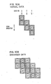
- Fine line data is illustrated as data of one pel in width.
- FIG. 7A shows a modéL of normal nonenhanced data with a single pel foreground (black) line perpendicular to the scan direction A.
- the ine is comprised of six black pels 400.
- FIG. 7B shows the enhanced data model produced through use of the circuits explained herein.
- the black pels 400 have been expanded on the leading edge by a small added black area 401 and on the trailing edge by a small black area 402.
- Each of the six pels comprising the one pel line are expanded in a similar manner.
- FIG. 7C illustrates a model of the widened black line that the enhanced data of FIG. 7B will produce.
- FIG. 7D relates to FIG. 7A in that it provides a representation of the normal nonenhanced data on the photoreceptive surface showing the overlapping nature of the pel structure as the scan lines are produced.
- the all-white data of scan 1 overlaps with the data of scan 2 that contains the first black pel of the line.
- the all white pels of scan 8 overlap-with the last black pel of the line in scan 7.
- the result is a somewhat shortened black line at both ends. More importantly, note that there is a similar overlapping of white pels with the single black pel within the scan line itself resulting in a single black pel line width somewhat narrower than one pel size.
- FIG. 7E is a representation of a line on the photoreceptive surface as it appears through use of the enhanced data producing means of the instant invention. Note that in this case, the enhanced data is produced by turning the laser off sooner and on later thereby widening the line.
- FIG. 7F the actual printed output where line width has been increased in accordance with the enhanced data to assure quality-printing of a single pel wide line in the direction perpendicular to scan.
- FIG. 8A illustrates a model of normal, nonenhanced data for a line which is to be printed parallel to the scan direction.
- the line is one pel in width comprised of six pels 404.
- FIG. 8B is a model of the enhanced data showing that each black pel 404 has been surrounded on each side in a direction parallel to the scan direction by a leading gray pel 405 and a trailing gray pel 406.
- FIG. 8C is a model of the result whereby the single width black pel has been expanded by surrounding the black pel with directly adjacent gray pels.
- FIG. 8D is a representation of the nonenhanced single pel width line 407 on the photoreceptive surface in the direction parallel to scan. Because of the overlapping pel structure from scan line to scan line, the foreground line 407 is actually less than one pel in width.
- FIG. 8E shows a representation of the enhanced data on the photoreceptive surface where gray is placed at the data transitions from white to black and from black to white.
- FIG. 8F is the actual printed output where the black line has been expanded by the presence of the gray data. No gray is visible.
- FIG. 9 comprised of FIGS. 9A-9F, illustrates the effects of the enhancement circuits on the edges of slanted lines. That is, lines neither perpendicular to scan nor parallel to scan.
- FIG. 9A is a model of normal nonenhanced data where the black pels 410 provide a staircase effect on each transition from black to white and from white to black.
- FIG. 9B is a model of enhanced data showing the locating of gray pels at each transition from black to white and white to black.
- FIG. 9 C is a model of the output exhibiting reduced digitization due to the filling caused by gray energy density levels in the electrophotographic process. No gray is visible.
- FIG. 9D shows a representation of normal nonenhanced data as it might appear on a photoreceptive surface illustrating again the overlapping nature of the pel structure and a visible digitization effect.
- FIG. 9E is a representation of enhanced data on a photoreceptive surface where gray pels are located directly adjacent black pels on both sides of the.black lines.
- FIG . 9F is the actual printed output with the reduced digitization caused by the addition of black pels along the transition areas.
- FIG . 10A shows normal nonenhanced data where B 1 denotes a black pel in scan 1, B 2 denotes a black pel in scan 2, and B 3 denotes a black pel in scan 3.
- FIG. 10B shows the enhanced data produced by the circuits to be described below illustrating that the data in scan line 1 is first printed as gray then as black during the next scan line, and finally as gray again during the second succeeding scan line. In those pel locations where both black and gray coincide, the black overwrites - the gray.
- G 1 denotes a gray pel corresponding to the black pel in line 1.
- G 2 denotes a gray pel corresponding to the black pel in line 2
- G 3 denotes a gray pel corresponding to the black pel in line 3.
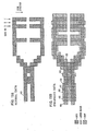
- FIG. 11A shows normal print output produced without the use of the print enhancement techniques of this invention.
- the scan direction is once again from top to bottom and successive lines are printed from right to left.
- FIG. 11B illustrates the same data shown in FIG. 11A where the print enhancement features of the circuits to be described below have been included.
- normal data 415 has been expanded at leading edges 416 and trailing edges 417 where the data 415 comprises a single pel line in a direction perpendicular to scan.
- Gray pels .418 have been added at each transition from black to white or white to black.
- An exception to the above description is shown at pel location 419 in which a gray pel appears but the added black at the trailing and leading edges of single pel line have' been inhibited. This condition is also present at pel location 420. Note also that pel location 420 would receive both a trailing gray and a leading gray signal. The trailing gray signal is inhibited in the implementation described below.
- FIGS. 7-11 show a print enhancement technique which meets the objective of enabling reliable printing of single pel data while simultaneously reducing digitization errors in the slanted character strokes. It differs from the related patent applications named above in that it combines both single pel and edge (smoothing) enhancements into a single enhancement technique. Combining the two enhancements into one is not simply a superimposition of the two techniques; if that were done, it would lead to interactions which would actually degrade print quality.
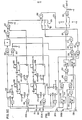
- FIG. 3 is a block diagram showing the position of circuit components to enhance the printed image according to this invention and is directed to an embodiment for use with the' electrophotographic laser printer shown in FIGS. 1 and 2.
- a character generator 200 provides signals to modulate the laser beam 15 (FIG. 2) to provide the desired characters. Data from the character generator is provided to laser drive circuitry 201.
- the circuit of this invention provides print enhancement circuits 202 between the character generator and the laser drive circuitry so that the enhancement techniques may be carried out.
- FIG. 4 is a more detailed block diagram of the enhancement circuitry 202.
- incoming data from the character generator is received on line 203 as input to the gray logic circuits 204 and the single line memory number one 205.
- the incoming data is analyzed so that gray pels may be produced corresponding to any foreground data on incoming line 203.
- Incoming data is clocked into single line memory number one 205 by memory control logic 206 from pel clock signals on line 207.
- the output of the gray logic circuit 204 is passed through the interaction logic 208 and the buffer 209 to appear on line 210 as input to the laser driver.
- the circuits shown in FIG. 4 produce gray pels corresponding to each of the black data on the first scan line.
- Second line data is also stored in single line memory 205.
- the first line data is clocked out of memory 205 to the black logic circuit 2 06 where the black data in the first scan line is then passed to the interaction logic circuit 208, buffer 209, and onto the laser driver.
- the black logic circuit 206 expands single pel black data occurring in a direction perpendicular to scan. Note also that as the data from the first scan line is read out of memory 205, it is also read into the single line memory number two, 211.
- the enhancement circuitry causes it to be printed as gray data; it is simultaneously stored in a single line memory.
- the next (second) line of data is generated, it is printed as gray and stored in a single line memory; the first line of data is read out of memory, printed as black, and is restored in a second memory.
- line 1 is read from the second memory and is printed once again as gray; line 2 is now printed as black and restored in the second memory; line 3 is printed as gray and is stored in the first memory. This process is repeated for each subsequent line. In this manner, each line is printed three times, first as gray, then as black, and then again as gray. It should be noted that black overwrites gray, that is, if both black and gray occur simultaneously, black is printed.
- the memory control logic 212 provides the proper clocking and read/write control functions required by the two single line memories.
- the black logic 206 detects single pel data and performs the necessary black data pulse width modifications.
- the gray logic 204 generates gray pulses of the proper predetermined width at the required pel positions.
- the interaction logic 208 examines both black and gray data and performs the logical functions necessary to provide the proper interaction responses, that is, to inhibit the expanded portion of a black signal under certain conditions or if both a leading and a trailing gray signal are present to inhibit one or the other.
- Buffer circuit 209 provides the voltage and current levels required by the laser driver.
- FIG. 5 is a detailed circuit diagram to implement the block diagram shown in FIG. 4.
- data signals are received from character generator 200 (FIG. 3) on .line 203 and are passed into latch 215.
- the output of latch 215 is passed into the gray logic circuit the first element of which is latch 216. Simultaneously, the output of latch 215 is passed over line 217 into the first memory 205.
- the output of latch 216 is connected to shift register 2l8. After the appropriate time delay, the output of shift register 218 is passed to OR circuit 219 before presentation to the single shot circuit 220.
- the output of single shot circuit 220 is passed to a second single shot circuit 221, the output of which represents a gray signal corresponding to black signals in the incoming data on the first line. In the terminology which will be used herein, this is termed leading gray data since they precede the black data of line one by one line.
- Circuits 222, 223, and 224 are counters - providing memory address control for both the first memory 205 and the second memory 211. In that manner, the data of line one is stored in memory 205 at the same time that it is processed in gray logic circuit 204 as described above.
- the output of memory 205 is connected through latch 225 to the input of second memory 211 where the first line is stored again during the reception of second line data.
- first line data the output of memory 211
- latch 216A is passed over line 226 to latch 216A.
- the output of. latch 216A is passed to shift register 218A.
- the output of circuit 218A is passed to OR circuit 219A and then into the first single shot 220A and the second single shot 221A.
- the output signal of 221A represents a gray signal corresponding to each black signal in the first data line, which data was printed as black on the preceding line. Therefore, in the terminology to be used herein, the output signal of circuit 221A is a trailing gray signal.
- the trailing gray and leading gray signals are passed to an AND circuit 227 and from there to OR circuit 228.
- OR circuit 228 is connected to the gray output line 229 which forms one of the signals passed to the output data line 210.
- Initialization of the circuits is accomplished by a start-of-scan signal provided over line 230 and the circuits are clocked by a clock signal provided over input line 231.
- latch 225 that is, the output of the first memory 205 is connected to the second memory 211 but is also connected over line 232 to latch 233.
- the output of latch 233 is sent to shift register 234 which is the first element of the black logic circuitry.
- the output delayed by three cycles appears on line 236.
- a delay of four cycles appears on line 237 and a delay of five cycles appears on line 238.
- OR circuit 239 adds the outputs on lines 235 and 236 and provides a signal to the preset input of latch 240.
- the output of latch 240 is added to the data signal on line 238 at OR circuit 241.
- the output of circuit 241 is sent to shift register 242 and also to delay line 243.
- Delay line 243 provides a variable time delay, the output of which is passed over line 244 to OR circuit 245.
- the output of OR circuit 245 is a leading black signal, that is, the added black signal appearing at the leading edge-of each single pel data in a direction perpendicular to scan.
- OR circuit 248 The output of OR circuit 248 is termed the trailing black signal and represents that added black portion on the trailing edge of single pel data in a direction perpendicular to scan.
- the trailing black signal and the leading black signal are ANDed together by circuit 249 and sent to AND circuit 250 where added black signals are ANDed with the data signals delayed by five cycles from shift register 234.
- the latter signal represents the black data signal in the line to be printed.
- the output of circuit 250 contains both leading black, added black and black data signals for the line to be printed.
- this black data is sent to the AND circuit 252 wherein the black signals are ANDed with the gray signals and sent across output line 210 to the laser drive circuit.
- OR circuit 251 provides an inhibition of added black signals under certain conditions.
- the inhibiting circuits include OR gates 253 and 254 with inverting circuit 255.
- the ability to program the type of inhibiting possible is provided by AND gate 256, inverter 257, and the three position switch 258.
- Another inhibiting circuit relating to a combination of leading gray pels and trailing gray pels in the same pel area involves the inverting OR gate 259 and OR gate 260.
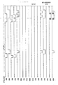
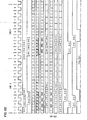
- FIG. 6 is a timing diagram which will be used to explain the operation of the circuit shown in FIG. 5.
- FIG. 6 shows four lines of data, each line comprised of nine pels, that is, nine clock cycles.
- the CK signal shows the clock cycle input to the circuits of FIG. 5 through input line 231.
- the data input signals DI are shown and are input to the circuits of FIG. 5 on line 203.
- the illustrative data input shown in FIG. 6 provides an all white signal in line 1 except for one black pel occurring at the first pel location. In line 2, an all white signal is present except for two black pels occurring at pel locations 1 and 2. In line 3, two black pels occur at locations 2 and 3.
- Signals 217S of FIG. 6 are the incoming data signals 217S on line 217, that is, the output of the latch 215. The effect of the latch is to delay the incoming data by one-half cycle.
- FIG. 6 show the memory address control signals output from counters 222, 223 and. 224.
- the R/ W signals of FIG. 6 show the read/write memory cycle.
- Signals 205S show that the output of the first memory 205 is read out on one half cycle.
- the second half cycle is a high impedance half cycle in which no data is read from the memory.
- Signals 225S show the output of memory 1 after being latched for a full cycle in latch 225.
- Signals 225S are input to the second memory 211 and are also processed in the black logic circuit before delivery to the laser printhead.
- Signals 226S are the output of the second memory 211.
- signals 216S are the input to the gray logic circuit and are the same as the data in signals delayed by one cycle.
- the data in signal at line 203 will be presented to the printhead as gray signals but will have been delayed by six cycles, that is, six pel areas. In a printer with the resolution of 95 pels per cm, the resultant displacement of data is about .74 millimeters. Thus, in a scanning system which scans from top to bottom, the data is moved down the page by .74 millimeters as a result of processing by the print enhancement circuit of FIG. 5. As already mentioned, line 1 is printed as gray data as it is put into the circuit and is delayed and printed as black data during the printing of the second line.
- the data of each line is printed as black data after a shift toward the left of one pel.
- the total shifting occurring as a result of the implementation shown in FIG. 5 is therefore six pels down (in the scan direction) and one pel left (a direction parallel to scan).
- signal level representation of signal 216AS is illustrated. This signal is processed to produce the trailing gray area and corresponds to the data in line 1 delayed by two lines, that is, it corresponds to the output of black data from memory 2.
- the data to be printed is the output of memory 1, that is, signal 225S.
- a black data signal corresponding to the black data signal input from line 1 is processed during the input of line 2.
- the output of shift register 234 signals 234D1-D5 are the data shifted by one to five cycles. It should be observed from FIG. 5 that signal 234D5 corresponds to the input data delayed by six cycles and it is this data that is the print data supplied to AND circuit 250, OR circuit 251, and to the data out signal on line 210. Note that signal 234D5 represents the black print data and it is to this data that the gray and added black signals will be added.
- Signals 239S of FIG. 6 represent the output of OR circuit 239 (FIG. 5) which adds data signals 234D2 and 234 D 3.
- line 1 data the output of memory 1
- signals 234D2 and 234D3 do not overlap since the input data is only a single pel wide.
- signals 234D2 and 234D3 overlap such that an output low signal appears.
- Signals 239S are latched at latch 240 which produces output signals 240S. Those signals are added to data signals 234D4 by OR gate 241 providing signals 241S.
- signals 241S contain a low signal corresponding to the presence of single pel data such as was present at line 1 but contain no low signal when multiple pel data is present such as in lines 2 and 3. Therefore, the function of circuits 239, 240, and 241 is to isolate one pel data so that such data can be broadened in a direction perpendicular to ' scan. The circuits filter out multiple pel data. The remainder of the black logic circuit acts upon signals 241S to provide the necessary expanded leading and lagging edges.
- Trailing edge expansion is provided by delay line 243. Trailing edge expansion is provided first by delaying signal 241S two cycles through shift register 242 and then acting upon those signals in delay line 246. Signals shown in FIG. 6 include the output of shift register 242 delayed by one and two cycles, that is, signals 242D1 and signals 242D2. The output signals for the delay circuits are shown at 246S and 244S. The leading black signals 245S are the output of OR circuit 245 which adds the delay signals 244S to signals 241S. Similarly, the signals to expand trailing edges are provided at signals 248S by adding the inverted delayed signals 248S with signals 242D2. Signals 249S represent the ANDing together of the leading edge and trailing edge expansion signals and signals 250S add the expansion signals to the data signals to provide the final print black signal.
- Circuit 251S acts upon the signals 250S to inhibit the added black expansion pulses if two of these pulses are in the same pel area together with a gray pulse.
- the example shown in FI G. 6 at 251S does not provide a pel area of that type.
- Signals 220S are fed to single shot 221 to provide output signals 221S.
- the length of signals 2215- are set by adjusting the resistor 221 R .
- single shot circuits 220 and 221 provide a shaping of the gray signal in which circuit 220 delays the leading edge of the signal in the pel period and circuit 221 sets the duration of the signal. In that manner, a signal pulse proper to provide a discharge of the photoconductor to the gray level is provided and can be positioned at any desired portion of the pel period.
- the trailing gray signals are provided in a manner similar to that for leading gray signals except that the input data comes from the output of memory 211, that-is, memory 2.
- Those signals 226S are provided to shift register 218A through latch 216A.
- Signals 218AS are shown on FIG. 6 and represent data from memory 2 delayed by an additional four cycles.
- Those signals are fed to latch 266 for a delay of an additional cycle as shown by signals 266S.
- OR circuit 219A adds signals 218AS with clock signals to provide signals 219AS.
- Those signals are used as input to single shot circuit 220A which sets the leading edge of the trailing gray signal as shown by signals 220AS.
- Those signals are used as input to single shot circuit 221A to set the duration of trailing gray pulses' as shown by signals 221AS.
- One of the requirements of the invention is to inhibit either the leading gray signal or the trailing gray signal when both of the signals occur in the same pel area.
- the reason for this is since the duration of the gray signals may not be exactly the same and since the signals may not be centered in the pel area, overlap of the two gray signals may produce an expanded signal which produces a black or nearly black signal.
- the circuit shown in FIG. 5 allows the leading gray signal to pass but inhibits the trailing gray signal whenever the two signals overlap. This is done by adding the leading gray signals 265S with the trailing gray signals 266S in OR circuit 259 to produce the signals 259S shown on FIG. 6. In the particular example shown on FIG. 6, such an overlapping gray condition is not illustrated.
- the leading gray signals would be added to the trailing gray signals 221AS at OR circuit 260 to provide signals 260S.
- trailing gray signals appear in signal 260S and none are inhibited.
- Signals 227S the output of circuit 227 shows the addition of signals 260S with signals 221S thus providing both leading and trailing gray signals together.
- Signal 227S may be connected to line 229 to provide the gray output signal to the laser printhead.
- signals 227S are provided to OR circuit 228 where the signals are added to an input determined by the position of switch 258. In switch position 1, the gray signal is inhibited if one added black signal occurs in the same pel area. In switch position 2, the gray signal is inhibited if two added blacks and a gray signal overlap while in switch position 3, the gray signal is passed unchanged.
- circuit 252 adds together pulses representing leading and trailing black pulses to provide a second input to circuit 254.
- Output signals 254S therefore represent signals showing an overlap of the gray area with two added black pulses. In the example shown in FIG . 6 , this condition has not occurred. If signals 254S provide an inhibiting pulse signal, that signal is sent to circuit 251 to inhibit the passage of the added black portions of signal 250S. To complete the description, FIG. 6 shows the black output signals 251S and the"final print output signals 252S combining both the black and gray signals. Signals 252S are sent over line 210 to modulate the printhead.
- the circuit provides edge enhancement or smoothing along diagonal lines by placing gray energy density levels along the irregular or digitized edge of slanted lines.
- the electrophotographic process causes the steps in the digitized edge to be partially filled in. This results in a more continuous or smoother character stroke.
- the circuit of FIG. 5 provides gray energy density levels by duty cycle modulating the laser printhead. The laser is turned off for a short period of time relative to the normal pel period to produce a gray level.
- Single pel lines parallel to the scan direction are enhanced by placing gray energy density levels on the photoreceptor along the edges of the lines. These gray levels are placed in the white space at both black to white and white to black transitions.
- the combined effects of the gray energy density levels in the electrophotographic process cause single pel lines parallel to the scan direction to be reliably printed. Since gray areas are placed only at transitions of lines parallel to the scan direction, stroke width variation in lines perpendicular to the scan direction are eliminated. Since gray is added at transitions of all parallel lines, not just single pel lines, a slight but not objectionable increase in stroke width occurs.
- the circuit provides for printing both one added black signal and a gray signal should they coincide in the same pel area.
- the circuit provides for inhibiting two added black pulses should they coincide with a gray pulse in the same pel area. Also, if two gray pulses coincide, the leading gray signal only is passed. Finally, if two added black signals coincide, both added black signals are passed. Provision is made for altering these interaction parameters if desired.
Abstract
Description
- This invention relates to printing machines such as an electrophotographic machine and more specifically relates to enhancing the printing of fine lines together with enhancing the printing of diagonal lines and provides for interactions between the enhancement techniques.
- US- A-4,460,909 relates to a method and apparatus for enhancing print produced by a printer such as an electrophotographic printer. In that invention, gray picture elements are added at certain transition areas between white and black picture elements. The purpose is to smooth transitions along diagonal lines where staircase effects are sometimes visible to the human eye.
- Many printing machines are designed to create an image by placing a series of picture elements (pels) on the image receiving material. For example, in electrophotographic printing machines, an image may be created by a light source which is caused to scan across photosensitive material in a succession of scan lines. The light beam places a series of overlapping pels on the charged surface of photosensitive material. Each pel is placed in a pel area and the light beam is modulated so that some pel areas are exposed to light and some are not. Wherever a pel containing light strikes the photosensitive material, it is discharged. In that manner, the photosensitive material is caused to bear a charge pattern of pels which images the subject that is being reproduced. The printed copy is obtained by developing the charge pattern and transferring the developed image to print material, usually paper.
- The resolution of images produced by a laser electrophotographic machine is generally stated in the number of pels produced per cm. For example, a 118-pel per cm electrophotographic printer has higher resolution than a 95- pels per cm printer. While the visual characteristics of print are generally better when a higher number of pels per cm are used, in one area the visual characteristics are made worse. That area is the printing of narrow fine lines, for example, lines of a single pel width. The reason is that as the number of pels per inch increase, the width of a single pel decreases. This decrease in pel width is made even more severe by the overlapping pel structure used in electrophotographic printing machines.
- At a resolution of 95 pels per cm, lines printed parallel or perpendicular to scan print with very little visible distortion. However, diagonal lines print with a staircase distortion which is quite visible to the human eye. Document US-A-4,460,909 describes apparatus and technique for smoothing the visible digitization present in diagonal lines.
- This invention provides apparatus and technique for enhancing the print quality of an electrophotographic printer or any printer capable of producing an intermediate visual level such as gray, a foreground visual level such as black, and a background visual level such as white. The invention combines techniques of smoothing digitized staircase effects with the technique of broadening fine lines.
- In performing the smoothing function, gray picture elements are produced along both edges of the slanted line. In the broadening function, gray picture elements are added directly adjacent foreground elements in a first dimension. In a second dimension perpendicular to the first dimension, expanded foreground picture elements are produced. In a scanning laser printer, the first dimension is parallel to the scan direction while the second dimension is perpendicular to the scan direction.
- In combining smoothing and broadening print enhancement techniques, various interactions are considered and enhanced pel producing signals are inhibited in some cases. For example, if a single pel area contains both an expanded pel signal and one gray pel signal, both enhancement signals are passed; if a single pel area contains both a "leading" gray signal and a "trailing" gray signal, one of the gray signals is inhibited; if a single pel area contains two expanded pel signals, i.e., a leading foreground signal and a trailing foreground signal, and a gray signal as well, only the gray signal is passed; and finally, if two expanded pel signals occur in the same pel area, both are passed.
- The above-mentioned and other features and objects of this invention and the manner of attaining them will become more apparent and the invention itself will best be understood by reference to the following description of embodiments of the invention taken in conjunction with the accompanying drawing, the description of which follows.
- FIG. 1 shows a typical electrophotographic printing machine.
- FIG. 2 shows solid-state laser apparatus for producing a scanning laser beam for the machine of FIG. 1.
- FIG. 3 is a block diagram showing the position of enhancement circuitry in accordance with this invention.
- FIG. 4 is a block diagram of the enhancement circuitry of FIG. 3.
- FIG. 5 is a detailed circuit diagram of a particular embodiment of the enhancement circuitry.
- FIG. 6 is a timing diagram for use with the circuit of FIG. 5.
- FIG. 7, comprised of FIGS. 7A-7F, are diagrams illustrating the enhancement of lines perpendicular to the scan direction.
- FIG. 8, comprised of FIGS. 8A-8F, illustrate the enhancement of lines parallel to the scan direction.
- FIG. 9, comprised of FIGS. 9A-9F, illustrate edge enhancement along slanted lines.
- FIG. 10, comprised of FIGS. 10A and 10B, show unenhanced data and the placement of gray energy density levels to enhance the same data in accordance with the circuit of FIG. 5.
- FIG. 11, comprised of FIGS. 11A and 11B, illustrate a representation of an unenhanced printed end result together with a representation of the same data enhanced in accordance with the circuit of FIG. 5.
- In electrophotographic printing machines, prints are produced by creating an electrostatic representation of the print on a photoreceptive surface, developing the image and then fusing the image to print material. In machines which utilize plain bond paper or other image receiving material not coated with photoreceptive material, the electrophotographic process is of the transfer type where photoreceptive material is placed around a rotating drum or arranged as a belt to be driven by a system of rollers. In a typical transfer process, photoreceptive material is passed under a stationary charge generating station to place a relatively uniform electrostatic charge, usually several hundred volts, across the entirety of the photoreceptive surface. Next, the photoreceptor is moved to an imaging station where it receives light rays generated by a light source. In electrophotographic printing machines such as the IBM 6670 Information Distributor, positive images are produced through the use of light rays which discharge the photoreceptive material in white or background. areas to relatively low levels while areas which are desired to print out as dark areas continue to carry high voltage levels after the exposure. In that manner, the photoreceptive material is caused to bear a positive charge pattern corresponding to the printing, shading, etc. which is desired. In the production of a negative image used in machines such as the IBM 3800 Electrophotographic Printer, light rays are used to discharge the photoreceptive material in the foreground areas (dark areas).
- After producing an image on the photoreceptor, the image is sent to a developing station where developing material called toner is placed on the image. This material may be in the form of a black powder or liquid and, in a system which produces a positive image; the material carries a charge opposite in polarity to the charge pattern on the photoreceptor. In a negative image system, the toner carries the same polarity as the charge on the photoreceptor. Because of the attraction of the charged toner to the photoreceptor, it adheres to the photoreceptor surface in proportions related to the shading of the image. -Thus, black character printing receives heavy toner deposits and white background areas should receive none.
- A developed image is moved from a developer to a transfer station where image receiving material, usually paper, is juxtaposed to the developed image on the photoreceptor. A charge is placed on the backside of the paper so that when the paper is stripped from the photoreceptor, the toner material is held on the paper and removed from the photoreceptor. The remaining process steps call for permanently bonding the transferred toner material to the paper and cleaning residual toner left on the photoreceptor after the transfer operation. Thereafter, the photoconductor is reused for subsequent print production.
- A common variation on the above-described process used in many electrophotographic machines, involves the use of specially prepared image receiving material which itself is coated with a photosensitive material. By utilizing that technique, the. image is electrostatically placed directly on the image receiving paper thereby avoiding the transfer operation. In this process, after exposure the paper is sent through a developer and then to a fuser for permanent bonding. Machines of this type avoid the residual toner problem and therefore avoid the need for cleaning stations. However, the resulting paper with its special photosensitive coating is more expensive than plain bond paper and special coating is considered to detract from the resulting product. As a consequence, coated paper machines are usually used only for low volume applications or where quality product is not essential.
- Production of the image on the photoreceptive surface can be produced by a scanning light beam where the desired characters are produced by driving a light generating source from information held in digital memory. The generating source may be a laser gun, an array of light-emitting diodes, etc. which direct light rays to the photoreceptor and cause it to bear the desired charge pattern.
- An example of a light scanning and printing system such as is employed in the IBM 6670 Information Distributor is disclosed in US -A- 3,750,189. In that system, a laser beam is directed through a collimating lens system and focused as a line on a rotating mirror. The reflected beam is passed through a combination of a toroidal and a spherical lens to focus the line image on the final image plane, that is, the photoreceptor. The shape of the focused beam on the, photoreceptor.is designed to be slightly elliptical in order to compensate for the different image forming properties of the optical system in the scan and nonscan directions.
- The type of light source provided in the IBM 6670 Information Distributor is a helium-neon laser generating source. This source provides a continuous laser beam which is modulated by an acousto-optic modulator to carry the digital information desired for reproduction. The current invention may be used with a helium-neon laser' source but the particular implementation to be described herein is designed for use with a solid-state laser source. Modulation of a solid-state laser source is usually accomplished by switching the laser beam on and off in accordance with the digital information desired for reproduction.
- Whether a continuous laser beam modulated by an acousto-optic modulator or a solid-state laser beam modulated by a switching circuit is used, the resultant image is formed by a series of overlapping picture elements, each picture element being small relatively circular dots placed adjacent to each other in an overlapping relationship. Adjacent pels overlap along each scan line and also overlap with adjacent pels on directly adjacent scan lines.
- FIG. 1 shows a typical electrophotographic laser printing machine. An
electrophotographic drum 11 is driven bymotor 90, in the direction of the arrow.Drum 11 carriesphotosensitive material 12 which passes under acharge corona generator 13 to charge the photoreceptive material to a suitable voltage. Next, thephotoreceptive material 12 is discharged atexposure station 16 in accordance with the image desired to be reproduced. That image is produced by amodule 14 consisting of a character generator and a laser printhead which produces the modulatedlaser beam 15. Next, the latent image is developed at thedeveloper station 51 and transferred by a transfer corona generator 52 to image receiving material (typically copy paper) traversing thepaper path 66.Photoreceptive material 12 then continues to the cleaningstation 53 before repeating the cycle to receive another image. Copy paper may be stored in eitherbin paper path 66 to agate 21. Copy paper is released bygate 21 and passed along the paper path through pinch rolls 20 through thetransfer station 52 and on to the fusing rolls 60. The finished print is then passed to anexit pocket 18 or to a finishingstation 17.Module 19 represents the control circuits which operate the machine in its intended manner and may be based on any suitable microprocessor or set of microprocessors. -
Optical system module 14 is shown in detail in FIG. 2 where a solid-state laser chip and a collimating lens are housed inassembly 100.Laser beam 15 passes fromassembly 100 throughcylindrical lens 101 to arotating mirror 102 which has a plurality of facets such asfacet 103 around its periphery. The laser beam is reflected from a single facet at a time in such a manner as to scan through an angle P. As each succeeding facet of therotating mirror 102 rotates into position to receivebeam 15, another scan through the angle P begins. Upon reflection from the rotating mirror facet, the laser beam is passed throughassembly 104 at which a toroidal lens and a spherical lens are used to finally shape the beam and to focus it on thephotoreceptive surface 12 shown in FIG. 1. Abeam fold mirror 105 is shown in both FIGS. 1 and 2 illustrating the final folding mechanism to direct the laser beam to thephotoreceptive surface 12.Motor 106 is provided to drive therotating mirror 102 while a start-of-scan mirror 107 is provided to direct the laser beam to a start-of-scan detector 108. - It should be noted that a single scan line on
photoreceptive material 12 is produced by the reflection of the laser beam across a single facet on rotatingmirror 102. The scan line is comprised of a succession of overlapping picture elements (pels) which may be, for example, 95 pels per cm. In such a case, each square cm on the photoconductor would carry 95 x 95 pels. The photoreceptor may be scanned in either a vertical or a horizontal direction relative to the receiving material, it may be scanned from either left or right, the scan can proceed from top to bottom, or bottom to top depending upon the particular implementation in the machine. Finally, to produce a positive image, the light beam is modulated to print the background while in a negative system the laser beam is modulated to produce the printing. - Before describing the particular embodiment in the implementing circuits shown in FIGS. 3-6, reference is made to FIGS. 7-10. These figures illustrate the results obtained through use of the print enhancement technique. The figures illustrate results obtained regardless of whether positive or negative development occurs. Fine line data is illustrated as data of one pel in width.
- FIG. 7A shows a modéL of normal nonenhanced data with a single pel foreground (black) line perpendicular to the scan direction A. The ine is comprised of six
black pels 400. FIG. 7B shows the enhanced data model produced through use of the circuits explained herein. In this case, theblack pels 400 have been expanded on the leading edge by a small addedblack area 401 and on the trailing edge by a smallblack area 402. Each of the six pels comprising the one pel line are expanded in a similar manner. - FIG. 7C illustrates a model of the widened black line that the enhanced data of FIG. 7B will produce.
- FIG. 7D relates to FIG. 7A in that it provides a representation of the normal nonenhanced data on the photoreceptive surface showing the overlapping nature of the pel structure as the scan lines are produced. Note that the all-white data of
scan 1 overlaps with the data ofscan 2 that contains the first black pel of the line. Similarly, the all white pels ofscan 8 overlap-with the last black pel of the line inscan 7. The result is a somewhat shortened black line at both ends. More importantly, note that there is a similar overlapping of white pels with the single black pel within the scan line itself resulting in a single black pel line width somewhat narrower than one pel size. - FIG. 7E is a representation of a line on the photoreceptive surface as it appears through use of the enhanced data producing means of the instant invention. Note that in this case, the enhanced data is produced by turning the laser off sooner and on later thereby widening the line.
- FIG. 7F the actual printed output where line width has been increased in accordance with the enhanced data to assure quality-printing of a single pel wide line in the direction perpendicular to scan.
- FIG. 8A illustrates a model of normal, nonenhanced data for a line which is to be printed parallel to the scan direction. In this data model, the line is one pel in width comprised of six pels 404.
- FIG. 8B is a model of the enhanced data showing that each
black pel 404 has been surrounded on each side in a direction parallel to the scan direction by a leadinggray pel 405 and a trailinggray pel 406. - FIG. 8C is a model of the result whereby the single width black pel has been expanded by surrounding the black pel with directly adjacent gray pels.
- , FIG. 8D is a representation of the nonenhanced single
pel width line 407 on the photoreceptive surface in the direction parallel to scan. Because of the overlapping pel structure from scan line to scan line, theforeground line 407 is actually less than one pel in width. - FIG. 8E shows a representation of the enhanced data on the photoreceptive surface where gray is placed at the data transitions from white to black and from black to white.
- FIG. 8F is the actual printed output where the black line has been expanded by the presence of the gray data. No gray is visible.
- FIG. 9, comprised of FIGS. 9A-9F, illustrates the effects of the enhancement circuits on the edges of slanted lines. That is, lines neither perpendicular to scan nor parallel to scan. FIG. 9A is a model of normal nonenhanced data where the
black pels 410 provide a staircase effect on each transition from black to white and from white to black. - FIG. 9B is a model of enhanced data showing the locating of gray pels at each transition from black to white and white to black.
- FIG. 9C is a model of the output exhibiting reduced digitization due to the filling caused by gray energy density levels in the electrophotographic process. No gray is visible.
- FIG. 9D shows a representation of normal nonenhanced data as it might appear on a photoreceptive surface illustrating again the overlapping nature of the pel structure and a visible digitization effect.
- FIG. 9E is a representation of enhanced data on a photoreceptive surface where gray pels are located directly adjacent black pels on both sides of the.black lines.
- FIG. 9F is the actual printed output with the reduced digitization caused by the addition of black pels along the transition areas.
- FIG. 10A shows normal nonenhanced data where B1 denotes a black pel in
scan 1, B2 denotes a black pel inscan 2, and B3 denotes a black pel inscan 3. - FIG. 10B shows the enhanced data produced by the circuits to be described below illustrating that the data in
scan line 1 is first printed as gray then as black during the next scan line, and finally as gray again during the second succeeding scan line. In those pel locations where both black and gray coincide, the black overwrites-the gray. In the illustration shown in FIG. 10B, G1 denotes a gray pel corresponding to the black pel inline 1. Similarly, G2 denotes a gray pel corresponding to the black pel inline 2 and G3 denotes a gray pel corresponding to the black pel inline 3. - FIG. 11A shows normal print output produced without the use of the print enhancement techniques of this invention. In FIG. 11A, the scan direction is once again from top to bottom and successive lines are printed from right to left.
- FIG. 11B illustrates the same data shown in FIG. 11A where the print enhancement features of the circuits to be described below have been included. In FIG. 11B,
normal data 415 has been expanded at leadingedges 416 and trailingedges 417 where thedata 415 comprises a single pel line in a direction perpendicular to scan. Gray pels .418 have been added at each transition from black to white or white to black. An exception to the above description is shown atpel location 419 in which a gray pel appears but the added black at the trailing and leading edges of single pel line have' been inhibited. This condition is also present atpel location 420. Note also thatpel location 420 would receive both a trailing gray and a leading gray signal. The trailing gray signal is inhibited in the implementation described below. - FIGS. 7-11 show a print enhancement technique which meets the objective of enabling reliable printing of single pel data while simultaneously reducing digitization errors in the slanted character strokes. It differs from the related patent applications named above in that it combines both single pel and edge (smoothing) enhancements into a single enhancement technique. Combining the two enhancements into one is not simply a superimposition of the two techniques; if that were done, it would lead to interactions which would actually degrade print quality.
- FIG. 3 is a block diagram showing the position of circuit components to enhance the printed image according to this invention and is directed to an embodiment for use with the' electrophotographic laser printer shown in FIGS. 1 and 2. A
character generator 200 provides signals to modulate the laser beam 15 (FIG. 2) to provide the desired characters. Data from the character generator is provided tolaser drive circuitry 201. As shown in FIG. 3, the circuit of this invention providesprint enhancement circuits 202 between the character generator and the laser drive circuitry so that the enhancement techniques may be carried out. - FIG. 4 is a more detailed block diagram of the
enhancement circuitry 202. In FIG. 4, incoming data from the character generator is received online 203 as input to thegray logic circuits 204 and the single line memory number one 205. In thelogic circuit 204, the incoming data is analyzed so that gray pels may be produced corresponding to any foreground data onincoming line 203. Incoming data is clocked into single line memory number one 205 bymemory control logic 206 from pel clock signals online 207. It should be noted that the output of thegray logic circuit 204 is passed through theinteraction logic 208 and thebuffer 209 to appear online 210 as input to the laser driver. Thus, the circuits shown in FIG. 4 produce gray pels corresponding to each of the black data on the first scan line. - When data for the second scan line appears on
line 203, that data is clocked intogray logic circuit 204 and on to the laser driver. Second line data is also stored insingle line memory 205. At the same time, the first line data is clocked out ofmemory 205 to the black logic circuit 206 where the black data in the first scan line is then passed to theinteraction logic circuit 208,buffer 209, and onto the laser driver. Theblack logic circuit 206 expands single pel black data occurring in a direction perpendicular to scan. Note also that as the data from the first scan line is read out ofmemory 205, it is also read into the single line memory number two, 211. - When data corresponding to the third scan line appears on
line 203, it is sent to thegray logic circuit 204 and on to the laser driver. Third line data is also read intomemory 205. Simultaneously, data fromscan line 2 is read out ofmemory 205 into theblack logic 206 and on to the laser driver. Second line data is also read intomemory 211. Also simultaneously, data from the first scan line is read out of thesingle line memory 211 into thegray logic circuit 204 and on to the laser driver. - To summarize the operations shown in FIG. 4, when the line of data is generated by the character generator, the enhancement circuitry causes it to be printed as gray data; it is simultaneously stored in a single line memory. When the next (second) line of data is generated, it is printed as gray and stored in a single line memory; the first line of data is read out of memory, printed as black, and is restored in a second memory. When the third line of data is generated,
line 1 is read from the second memory and is printed once again as gray;line 2 is now printed as black and restored in the second memory;line 3 is printed as gray and is stored in the first memory. This process is repeated for each subsequent line. In this manner, each line is printed three times, first as gray, then as black, and then again as gray. It should be noted that black overwrites gray, that is, if both black and gray occur simultaneously, black is printed. - Note that the
memory control logic 212 provides the proper clocking and read/write control functions required by the two single line memories. Theblack logic 206 detects single pel data and performs the necessary black data pulse width modifications. Thegray logic 204 generates gray pulses of the proper predetermined width at the required pel positions. Theinteraction logic 208 examines both black and gray data and performs the logical functions necessary to provide the proper interaction responses, that is, to inhibit the expanded portion of a black signal under certain conditions or if both a leading and a trailing gray signal are present to inhibit one or the other.Buffer circuit 209 provides the voltage and current levels required by the laser driver. - FIG. 5 is a detailed circuit diagram to implement the block diagram shown in FIG. 4. In FIG. 5, data signals are received from character generator 200 (FIG. 3) on .
line 203 and are passed intolatch 215. The output oflatch 215 is passed into the gray logic circuit the first element of which islatch 216. Simultaneously, the output oflatch 215 is passed overline 217 into thefirst memory 205. - Continuing first with a description of the gray logic, note that the output of
latch 216 is connected to shift register 2l8. After the appropriate time delay, the output ofshift register 218 is passed to ORcircuit 219 before presentation to thesingle shot circuit 220. The output ofsingle shot circuit 220 is passed to a secondsingle shot circuit 221, the output of which represents a gray signal corresponding to black signals in the incoming data on the first line. In the terminology which will be used herein, this is termed leading gray data since they precede the black data of line one by one line. - Returning now to the output of
latch 215, note that it is transferred overline 217 to thefirst memory 205.Circuits first memory 205 and thesecond memory 211. In that manner, the data of line one is stored inmemory 205 at the same time that it is processed ingray logic circuit 204 as described above. - The output of
memory 205 is connected throughlatch 225 to the input ofsecond memory 211 where the first line is stored again during the reception of second line data. When the third line data is received, first line data, the output ofmemory 211, is passed overline 226 to latch 216A. The output of. latch 216A is passed to shiftregister 218A. After the appropriate time delay, the output ofcircuit 218A is passed to ORcircuit 219A and then into the firstsingle shot 220A and the secondsingle shot 221A. The output signal of 221A represents a gray signal corresponding to each black signal in the first data line, which data was printed as black on the preceding line. Therefore, in the terminology to be used herein, the output signal ofcircuit 221A is a trailing gray signal. The trailing gray and leading gray signals are passed to an ANDcircuit 227 and from there to ORcircuit 228. ORcircuit 228 is connected to thegray output line 229 which forms one of the signals passed to theoutput data line 210. - Initialization of the circuits is accomplished by a start-of-scan signal provided over
line 230 and the circuits are clocked by a clock signal provided overinput line 231. - Note that the output of
latch 225, that is, the output of thefirst memory 205 is connected to thesecond memory 211 but is also connected overline 232 to latch 233. The output oflatch 233 is sent to shiftregister 234 which is the first element of the black logic circuitry. The output ofshift register 234, delayed by two cycles, appears online 235. The output delayed by three cycles appears online 236. A delay of four cycles appears online 237 and a delay of five cycles appears online 238. ORcircuit 239 adds the outputs onlines latch 240. The output oflatch 240 is added to the data signal online 238 at ORcircuit 241. The output ofcircuit 241 is sent to shiftregister 242 and also to delayline 243.Delay line 243 provides a variable time delay, the output of which is passed overline 244 to ORcircuit 245. The output of ORcircuit 245 is a leading black signal, that is, the added black signal appearing at the leading edge-of each single pel data in a direction perpendicular to scan. - Note that the output of
shift register 242 is sent tovariable delay line 246 the output of which is connected throughinverter 247 to ORcircuit 248. The output of ORcircuit 248 is termed the trailing black signal and represents that added black portion on the trailing edge of single pel data in a direction perpendicular to scan. The trailing black signal and the leading black signal are ANDed together bycircuit 249 and sent to ANDcircuit 250 where added black signals are ANDed with the data signals delayed by five cycles fromshift register 234. The latter signal represents the black data signal in the line to be printed. As a consequence, the output ofcircuit 250 contains both leading black, added black and black data signals for the line to be printed. After passing through ORcircuit 251, this black data is sent to the ANDcircuit 252 wherein the black signals are ANDed with the gray signals and sent acrossoutput line 210 to the laser drive circuit. ORcircuit 251 provides an inhibition of added black signals under certain conditions. - The inhibiting circuits include OR
gates circuit 255. The ability to program the type of inhibiting possible is provided by ANDgate 256,inverter 257, and the threeposition switch 258. Another inhibiting circuit relating to a combination of leading gray pels and trailing gray pels in the same pel area involves the inverting ORgate 259 andOR gate 260. - FIG. 6 is a timing diagram which will be used to explain the operation of the circuit shown in FIG. 5. FIG. 6 shows four lines of data, each line comprised of nine pels, that is, nine clock cycles.
- The CK signal shows the clock cycle input to the circuits of FIG. 5 through
input line 231. The data input signals DI are shown and are input to the circuits of FIG. 5 online 203. The illustrative data input shown in FIG. 6 provides an all white signal inline 1 except for one black pel occurring at the first pel location. Inline 2, an all white signal is present except for two black pels occurring atpel locations line 3, two black pels occur atlocations line 217, that is, the output of thelatch 215. The effect of the latch is to delay the incoming data by one-half cycle. The MAC signals of FIG. 6 show the memory address control signals output fromcounters - Signals 205S show that the output of the
first memory 205 is read out on one half cycle. The second half cycle is a high impedance half cycle in which no data is read from the memory. Signals 225S show the output ofmemory 1 after being latched for a full cycle inlatch 225. Signals 225S are input to thesecond memory 211 and are also processed in the black logic circuit before delivery to the laser printhead. Signals 226S are the output of thesecond memory 211. Finally, signals 216S are the input to the gray logic circuit and are the same as the data in signals delayed by one cycle. - After all processing takes place in the logic circuits of FIG. 5, the data in signal at
line 203 will be presented to the printhead as gray signals but will have been delayed by six cycles, that is, six pel areas. In a printer with the resolution of 95 pels per cm, the resultant displacement of data is about .74 millimeters. Thus, in a scanning system which scans from top to bottom, the data is moved down the page by .74 millimeters as a result of processing by the print enhancement circuit of FIG. 5. As already mentioned,line 1 is printed as gray data as it is put into the circuit and is delayed and printed as black data during the printing of the second line. Therefore, in a scanning system which scans from right to left, the data of each line is printed as black data after a shift toward the left of one pel. The total shifting occurring as a result of the implementation shown in FIG. 5 is therefore six pels down (in the scan direction) and one pel left (a direction parallel to scan). - Continuing now with a description of the timing circuit shown in FIG. 6, a signal level representation of signal 216AS is illustrated. This signal is processed to produce the trailing gray area and corresponds to the data in
line 1 delayed by two lines, that is, it corresponds to the output of black data frommemory 2. - The data to be printed is the output of
memory 1, that is, signal 225S. As shown on FIG. 6, a black data signal corresponding to the black data signal input fromline 1 is processed during the input ofline 2. The output ofshift register 234 signals 234D1-D5 are the data shifted by one to five cycles. It should be observed from FIG. 5 that signal 234D5 corresponds to the input data delayed by six cycles and it is this data that is the print data supplied to ANDcircuit 250, ORcircuit 251, and to the data out signal online 210. Note that signal 234D5 represents the black print data and it is to this data that the gray and added black signals will be added. - Signals 239S of FIG. 6 represent the output of OR circuit 239 (FIG. 5) which adds data signals 234D2 and 234D3. During the processing of
line 1 data (the output of memory 1) , signals 234D2 and 234D3 do not overlap since the input data is only a single pel wide. During the processing ofline 2, however, which occurs during the input ofline 3, signals 234D2 and 234D3 overlap such that an output low signal appears. Signals 239S are latched atlatch 240 which produces output signals 240S. Those signals are added to data signals 234D4 byOR gate 241 providingsignals 241S. The observation may be made thatsignals 241S contain a low signal corresponding to the presence of single pel data such as was present atline 1 but contain no low signal when multiple pel data is present such as inlines circuits signals 241S to provide the necessary expanded leading and lagging edges. - The leading edge expansion is provided by
delay line 243. Trailing edge expansion is provided first by delayingsignal 241S two cycles throughshift register 242 and then acting upon those signals indelay line 246. Signals shown in FIG. 6 include the output ofshift register 242 delayed by one and two cycles, that is, signals 242D1 and signals 242D2. The output signals for the delay circuits are shown at 246S and 244S. The leading black signals 245S are the output of ORcircuit 245 which adds the delay signals 244S to signals 241S. Similarly, the signals to expand trailing edges are provided at signals 248S by adding the inverted delayed signals 248S with signals 242D2. Signals 249S represent the ANDing together of the leading edge and trailing edge expansion signals and signals 250S add the expansion signals to the data signals to provide the final print black signal. -
Circuit 251S acts upon thesignals 250S to inhibit the added black expansion pulses if two of these pulses are in the same pel area together with a gray pulse. The example shown in FIG. 6 at 251S does not provide a pel area of that type. - The following signal representations to be described from FIG. 6 will illustrate the operation of the gray logic circuits. Already noted above is the fact that the leading gray signals are derived directly from the data in on
line 203. These signals are fed throughlatches shift register 218 which delays the data signals by four pels as shown at signals 218S on FIG. 6. An added pel of delay is provided bylatch 265 such that signals 265S represent the input signal delayed by six pels. Signals 219S represent the adding of the clock signal with signals 218S. This signal is 'used as input tosingle shot circuit 220 to providesignals 220S.Single shot 220 operates to delay the output signals 220S by an amount determined by setting the adjustingresistor 220R. Signals 220S are fed tosingle shot 221 to provide output signals 221S. The length of signals 2215- are set by adjusting theresistor 221R. Thus,single shot circuits circuit 220 delays the leading edge of the signal in the pel period andcircuit 221 sets the duration of the signal. In that manner, a signal pulse proper to provide a discharge of the photoconductor to the gray level is provided and can be positioned at any desired portion of the pel period. - The trailing gray signals are provided in a manner similar to that for leading gray signals except that the input data comes from the output of
memory 211, that-is,memory 2. Those signals 226S are provided to shiftregister 218A throughlatch 216A. Signals 218AS are shown on FIG. 6 and represent data frommemory 2 delayed by an additional four cycles. Those signals are fed to latch 266 for a delay of an additional cycle as shown bysignals 266S. ORcircuit 219A adds signals 218AS with clock signals to provide signals 219AS. Those signals are used as input tosingle shot circuit 220A which sets the leading edge of the trailing gray signal as shown by signals 220AS. Those signals are used as input tosingle shot circuit 221A to set the duration of trailing gray pulses' as shown by signals 221AS. - One of the requirements of the invention is to inhibit either the leading gray signal or the trailing gray signal when both of the signals occur in the same pel area. The reason for this is since the duration of the gray signals may not be exactly the same and since the signals may not be centered in the pel area, overlap of the two gray signals may produce an expanded signal which produces a black or nearly black signal. The circuit shown in FIG. 5 allows the leading gray signal to pass but inhibits the trailing gray signal whenever the two signals overlap. This is done by adding the leading
gray signals 265S with the trailinggray signals 266S in ORcircuit 259 to produce thesignals 259S shown on FIG. 6. In the particular example shown on FIG. 6, such an overlapping gray condition is not illustrated. Were there such a condition, the leading gray signals would be added to the trailing gray signals 221AS atOR circuit 260 to providesignals 260S. In the example shown in FIG. 6, trailing gray signals appear insignal 260S and none are inhibited. Signals 227S, the output ofcircuit 227 shows the addition ofsignals 260S with signals 221S thus providing both leading and trailing gray signals together. Signal 227S may be connected toline 229 to provide the gray output signal to the laser printhead. However, in the circuit of FIG. 5, signals 227S are provided to ORcircuit 228 where the signals are added to an input determined by the position ofswitch 258. Inswitch position 1, the gray signal is inhibited if one added black signal occurs in the same pel area. Inswitch position 2, the gray signal is inhibited if two added blacks and a gray signal overlap while inswitch position 3, the gray signal is passed unchanged. - In the operation of the
signal inhibiting circuits signals 267S. Circuit 252 adds together pulses representing leading and trailing black pulses to provide a second input tocircuit 254. Output signals 254S therefore represent signals showing an overlap of the gray area with two added black pulses. In the example shown in FIG. 6, this condition has not occurred. Ifsignals 254S provide an inhibiting pulse signal, that signal is sent tocircuit 251 to inhibit the passage of the added black portions ofsignal 250S. To complete the description, FIG. 6 shows theblack output signals 251S and the"final print output signals 252S combining both the black and gray signals. Signals 252S are sent overline 210 to modulate the printhead. - From the above description of the circuit and its operation, it may be observed that data is printed one line removed from its actual reception, that is, data that would ordinarily go to the printhead for
line 1 is actually printed online 2 because of the presence of the enhancement circuits. The data that is printed atline '1 are leading gray pels which correspond to the black pels to be printed inline 2 and whenline 3 is reached, trailing gray pels are printed corresponding to the black data printed inline 2. If there are black data inline 3 overlapping with the gray signals, the black signals override the gray. It may also be observed that single pel data is isolated in order that it can be broadened in a direction perpendicular to scan. Black is added to single pel data only. - The circuit provides edge enhancement or smoothing along diagonal lines by placing gray energy density levels along the irregular or digitized edge of slanted lines. The electrophotographic process causes the steps in the digitized edge to be partially filled in. This results in a more continuous or smoother character stroke. The circuit of FIG. 5 provides gray energy density levels by duty cycle modulating the laser printhead. The laser is turned off for a short period of time relative to the normal pel period to produce a gray level.
- Single pel lines parallel to the scan direction are enhanced by placing gray energy density levels on the photoreceptor along the edges of the lines. These gray levels are placed in the white space at both black to white and white to black transitions. The combined effects of the gray energy density levels in the electrophotographic process cause single pel lines parallel to the scan direction to be reliably printed. Since gray areas are placed only at transitions of lines parallel to the scan direction, stroke width variation in lines perpendicular to the scan direction are eliminated. Since gray is added at transitions of all parallel lines, not just single pel lines, a slight but not objectionable increase in stroke width occurs.
- Additionally, the circuit provides for printing both one added black signal and a gray signal should they coincide in the same pel area. The circuit provides for inhibiting two added black pulses should they coincide with a gray pulse in the same pel area. Also, if two gray pulses coincide, the leading gray signal only is passed. Finally, if two added black signals coincide, both added black signals are passed. Provision is made for altering these interaction parameters if desired.
Claims (11)
Applications Claiming Priority (2)
| Application Number | Priority Date | Filing Date | Title |
|---|---|---|---|
| US611561 | 1984-05-17 | ||
| US06/611,561 US4625222A (en) | 1984-05-17 | 1984-05-17 | Interacting print enhancement techniques |
Publications (3)
| Publication Number | Publication Date |
|---|---|
| EP0162259A2 true EP0162259A2 (en) | 1985-11-27 |
| EP0162259A3 EP0162259A3 (en) | 1986-06-25 |
| EP0162259B1 EP0162259B1 (en) | 1990-03-14 |
Family
ID=24449517
Family Applications (1)
| Application Number | Title | Priority Date | Filing Date |
|---|---|---|---|
| EP85104231A Expired EP0162259B1 (en) | 1984-05-17 | 1985-04-11 | Interacting print enhancement techniques |
Country Status (4)
| Country | Link |
|---|---|
| US (1) | US4625222A (en) |
| EP (1) | EP0162259B1 (en) |
| JP (1) | JPS60251761A (en) |
| DE (1) | DE3576587D1 (en) |
Cited By (4)
| Publication number | Priority date | Publication date | Assignee | Title |
|---|---|---|---|---|
| GB2199967A (en) * | 1987-01-13 | 1988-07-20 | Plessey Co Plc | Character enhancement systems |
| EP0508727A2 (en) * | 1991-04-08 | 1992-10-14 | Matsushita Electric Industrial Co., Ltd. | Image processing apparatus |
| EP0582369A1 (en) * | 1992-05-28 | 1994-02-09 | Xerox Corporation | Bit-map image resolution converter with controlled compensation for write-white xerographic laser printer |
| US5555557A (en) * | 1990-04-23 | 1996-09-10 | Xerox Corporation | Bit-map image resolution converter with controlled compensation for write-white xerographic laser printing |
Families Citing this family (55)
| Publication number | Priority date | Publication date | Assignee | Title |
|---|---|---|---|---|
| US4707709A (en) * | 1986-01-17 | 1987-11-17 | Eastman Kodak Company | Image recording apparatus in which exposure levels are a function of image contents |
| US4884857A (en) * | 1987-11-09 | 1989-12-05 | International Business Machines Corporation | Scanner for use in multiple spot laser electrophotographic printer |
| US4967211A (en) * | 1988-06-14 | 1990-10-30 | International Business Machines Corporation | Printing machine with toner density balance in solid areas and line strokes |
| US5005139A (en) | 1988-08-16 | 1991-04-02 | Hewlett-Packard Company | Piece-wise print image enhancement for dot matrix printers |
| KR940010876B1 (en) * | 1989-04-17 | 1994-11-19 | 도오꾜오 덴끼 가부시끼가이샤 | Image printing method for edge emission type el printer |
| US6529637B1 (en) | 1989-05-22 | 2003-03-04 | Pixel Instruments Corporation | Spatial scan replication circuit |
| US5424780C1 (en) * | 1989-05-22 | 2002-07-23 | James C Cooper | Apparatus and method for special scan modulation of a video display |
| US7382929B2 (en) | 1989-05-22 | 2008-06-03 | Pixel Instruments Corporation | Spatial scan replication circuit |
| US5045952A (en) * | 1989-08-21 | 1991-09-03 | Xerox Corporation | Method for edge enhanced error diffusion |
| US4933689A (en) * | 1989-10-25 | 1990-06-12 | Hewlett-Packard Company | Method and apparatus for print image enhancement |
| US5128698A (en) * | 1990-01-19 | 1992-07-07 | International Business Machines Corporation | Boldness control in an electrophotographic machine |
| JP2758262B2 (en) * | 1990-11-06 | 1998-05-28 | 沖電気工業株式会社 | Non-impact printer |
| US5134495A (en) * | 1990-11-07 | 1992-07-28 | Dp-Tek, Inc. | Resolution transforming raster-based imaging system |
| US5193008A (en) * | 1990-11-07 | 1993-03-09 | Dp-Tek, Inc. | Interleaving vertical pixels in raster-based laser printers |
| US5221971A (en) * | 1990-11-21 | 1993-06-22 | Polaroid Corporation | Area modulation printing apparatus |
| DE69108010T2 (en) * | 1990-11-21 | 1995-07-06 | Polaroid Corp | PRINTING DEVICE. |
| JP2651493B2 (en) * | 1990-11-21 | 1997-09-10 | スターリング ドライ イメイジング,インコーポレイテッド | Printing apparatus and method |
| US5170261A (en) * | 1990-11-21 | 1992-12-08 | Polaroid Corporation | Printing method |
| DE69220819T2 (en) * | 1991-02-01 | 1997-11-20 | Canon Kk | Image processing method and device |
| US6016154A (en) * | 1991-07-10 | 2000-01-18 | Fujitsu Limited | Image forming apparatus |
| JP2871195B2 (en) * | 1991-07-11 | 1999-03-17 | 京セラ株式会社 | Image smoothing processing device in printer |
| US5357273A (en) * | 1991-07-29 | 1994-10-18 | Xerox Corporation | Resolution conversion via intensity controlled overscanned illumination for optical printers and the like having high gamma photosensitive recording media |
| US8352400B2 (en) | 1991-12-23 | 2013-01-08 | Hoffberg Steven M | Adaptive pattern recognition based controller apparatus and method and human-factored interface therefore |
| US10361802B1 (en) | 1999-02-01 | 2019-07-23 | Blanding Hovenweep, Llc | Adaptive pattern recognition based control system and method |
| EP0604685A1 (en) * | 1992-12-28 | 1994-07-06 | Océ-Nederland B.V. | Method of modifying the fatness of characters |
| US5325211A (en) * | 1993-01-04 | 1994-06-28 | Xerox Corporation | Error diffusion with output and input based feedback |
| US5479175A (en) * | 1993-09-10 | 1995-12-26 | Xerox Corporation | Method and apparatus for enhancing discharged area developed regions in a tri-level pringing system |
| US5504462A (en) * | 1993-09-10 | 1996-04-02 | Xerox Corporation | Apparatus for enhancing pixel addressability in a pulse width and position modulated system |
| US5581292A (en) * | 1993-09-10 | 1996-12-03 | Xerox Corporation | Method and apparatus for enhancing charged area developed regions in a tri-level printing system |
| US5831657A (en) * | 1993-09-22 | 1998-11-03 | Kabushiki Kaisha Toshiba | Image forming system with smoothing pixels of a larger size |
| US5621546A (en) * | 1993-11-02 | 1997-04-15 | Xerox Corporation | Method and apparatus for vector error diffusion with output color control |
| US5359423A (en) * | 1993-12-17 | 1994-10-25 | Xerox Corporation | Method for statistical generation of density preserving templates for print enhancement |
| US5387985A (en) * | 1993-12-17 | 1995-02-07 | Xerox Corporation | Non-integer image resolution conversion using statistically generated look-up tables |
| US5696845A (en) * | 1993-12-17 | 1997-12-09 | Xerox Corporation | Method for design and implementation of an image resolution enhancement system that employs statistically generated look-up tables |
| US5724455A (en) * | 1993-12-17 | 1998-03-03 | Xerox Corporation | Automated template design method for print enhancement |
| US5579445A (en) * | 1993-12-17 | 1996-11-26 | Xerox Corporation | Image resolution conversion method that employs statistically generated multiple morphological filters |
| US5539866A (en) * | 1994-05-11 | 1996-07-23 | Xerox Corporation | Method and apparatus for accurately rendering half-bitted image pixels |
| JPH08204971A (en) * | 1994-10-31 | 1996-08-09 | Xerox Corp | Image compression method using predictive coding and error diffusion |
| US5493416A (en) * | 1994-10-31 | 1996-02-20 | Xerox Corporation | Method combining error diffusion and traditional halftoning with arbitrary screen orientation |
| US5680485A (en) * | 1994-12-19 | 1997-10-21 | Xerox Corporation | Method and apparatus employing erosion-based filter pairs for image mapping |
| US5666470A (en) * | 1995-06-29 | 1997-09-09 | Xerox Corporation | Method and apparatus for appearance tuning of bitmap images |
| US5687297A (en) * | 1995-06-29 | 1997-11-11 | Xerox Corporation | Multifunctional apparatus for appearance tuning and resolution reconstruction of digital images |
| US5729663A (en) * | 1995-12-07 | 1998-03-17 | Xerox Corporation | Method and apparatus for gray screening |
| US5668638A (en) * | 1996-06-27 | 1997-09-16 | Xerox Corporation | Error diffusion method with symmetric enhancement |
| JP3476331B2 (en) * | 1997-03-14 | 2003-12-10 | 株式会社東芝 | Image processing apparatus and image processing method |
| US6181438B1 (en) | 1997-05-05 | 2001-01-30 | Xerox Corporation | Method and apparatus for digital image darkness control using quantized fractional pixels |
| US6091891A (en) * | 1997-05-09 | 2000-07-18 | Lexmark International, Inc. | Method and apparatus for calibrating delay lines to create gray levels in continuous tone printing |
| US6266153B1 (en) | 1998-05-12 | 2001-07-24 | Xerox Corporation | Image forming device having a reduced toner consumption mode |
| US7966078B2 (en) | 1999-02-01 | 2011-06-21 | Steven Hoffberg | Network media appliance system and method |
| US6919973B1 (en) | 1999-07-27 | 2005-07-19 | Xerox Corporation | Auxiliary pixel patterns for improving print quality |
| US7016073B1 (en) | 1999-07-27 | 2006-03-21 | Xerox Corporation | Digital halftone with auxiliary pixels |
| US6970258B1 (en) | 1999-07-27 | 2005-11-29 | Xerox Corporation | Non-printing patterns for improving font print quality |
| US6606420B1 (en) | 1999-10-25 | 2003-08-12 | Xerox Corporation | Method and apparatus for digital image darkness control in saturated image structures |
| DE10211530A1 (en) * | 2002-03-15 | 2003-10-09 | Oce Printing Systems Gmbh | Electrophotographic process and printing system for generating a printed image |
| JP3982817B2 (en) * | 2003-03-07 | 2007-09-26 | 株式会社東芝 | Image processing apparatus and image processing method |
Citations (4)
| Publication number | Priority date | Publication date | Assignee | Title |
|---|---|---|---|---|
| DE3025267A1 (en) * | 1979-07-04 | 1981-01-15 | Fuji Photo Film Co Ltd | LASER BEAM RECORDING METHOD |
| EP0082281A1 (en) * | 1981-12-18 | 1983-06-29 | International Business Machines Corporation | Electrophotographic printer and method of electrophotographic printing |
| US4396928A (en) * | 1980-05-09 | 1983-08-02 | Hitachi, Ltd. | Printer controller for laser beam printer |
| US4437122A (en) * | 1981-09-12 | 1984-03-13 | Xerox Corporation | Low resolution raster images |
Family Cites Families (5)
| Publication number | Priority date | Publication date | Assignee | Title |
|---|---|---|---|---|
| JPS5129034A (en) * | 1974-09-05 | 1976-03-11 | Seikosha Kk | |
| JPS54102142A (en) * | 1978-01-30 | 1979-08-11 | Ricoh Co Ltd | Picture image restoration method in dot picture image |
| JPS56156855A (en) * | 1980-05-09 | 1981-12-03 | Hitachi Ltd | Print control system |
| JPS5767955A (en) * | 1980-10-16 | 1982-04-24 | Canon Inc | Image recorder |
| US4365275A (en) * | 1981-05-08 | 1982-12-21 | Delta Scan, Inc. | Method for producing images on radiation sensitive recording mediums |
-
1984
- 1984-05-17 US US06/611,561 patent/US4625222A/en not_active Expired - Lifetime
-
1985
- 1985-04-10 JP JP60074551A patent/JPS60251761A/en active Granted
- 1985-04-11 DE DE8585104231T patent/DE3576587D1/en not_active Revoked
- 1985-04-11 EP EP85104231A patent/EP0162259B1/en not_active Expired
Patent Citations (5)
| Publication number | Priority date | Publication date | Assignee | Title |
|---|---|---|---|---|
| DE3025267A1 (en) * | 1979-07-04 | 1981-01-15 | Fuji Photo Film Co Ltd | LASER BEAM RECORDING METHOD |
| US4396928A (en) * | 1980-05-09 | 1983-08-02 | Hitachi, Ltd. | Printer controller for laser beam printer |
| US4437122A (en) * | 1981-09-12 | 1984-03-13 | Xerox Corporation | Low resolution raster images |
| US4437122B1 (en) * | 1981-09-12 | 1993-03-30 | Xerox Corp | |
| EP0082281A1 (en) * | 1981-12-18 | 1983-06-29 | International Business Machines Corporation | Electrophotographic printer and method of electrophotographic printing |
Cited By (7)
| Publication number | Priority date | Publication date | Assignee | Title |
|---|---|---|---|---|
| GB2199967A (en) * | 1987-01-13 | 1988-07-20 | Plessey Co Plc | Character enhancement systems |
| GB2199967B (en) * | 1987-01-13 | 1990-12-05 | Plessey Co Plc | Improvements in or relating to character enhancement systems |
| US5555557A (en) * | 1990-04-23 | 1996-09-10 | Xerox Corporation | Bit-map image resolution converter with controlled compensation for write-white xerographic laser printing |
| EP0508727A2 (en) * | 1991-04-08 | 1992-10-14 | Matsushita Electric Industrial Co., Ltd. | Image processing apparatus |
| EP0508727A3 (en) * | 1991-04-08 | 1993-07-07 | Matsushita Electric Industrial Co., Ltd. | Image processing apparatus |
| US5361330A (en) * | 1991-04-08 | 1994-11-01 | Matsushita Electric Industrial Co., Ltd. | Image processing apparatus |
| EP0582369A1 (en) * | 1992-05-28 | 1994-02-09 | Xerox Corporation | Bit-map image resolution converter with controlled compensation for write-white xerographic laser printer |
Also Published As
| Publication number | Publication date |
|---|---|
| JPS60251761A (en) | 1985-12-12 |
| US4625222A (en) | 1986-11-25 |
| EP0162259A3 (en) | 1986-06-25 |
| JPH0362154B2 (en) | 1991-09-25 |
| DE3576587D1 (en) | 1990-04-19 |
| EP0162259B1 (en) | 1990-03-14 |
Similar Documents
| Publication | Publication Date | Title |
|---|---|---|
| US4625222A (en) | Interacting print enhancement techniques | |
| EP0163841B1 (en) | Fine line print enhancement | |
| EP0246457B1 (en) | Compensation for fine line prints | |
| EP0356038B1 (en) | Piece-wise printed image enhancement for dot matrix printers | |
| US4847641A (en) | Piece-wise print image enhancement for dot matrix printers | |
| US4933689A (en) | Method and apparatus for print image enhancement | |
| US5479175A (en) | Method and apparatus for enhancing discharged area developed regions in a tri-level pringing system | |
| US4241415A (en) | Masking device for selectively preventing visualization of data from a data output system | |
| EP0533346B1 (en) | A pulsed imaging, pulse width modulation raster output scanner for tri-level exposure | |
| EP0776121B1 (en) | Dot enhancement for laser imagers | |
| US5581292A (en) | Method and apparatus for enhancing charged area developed regions in a tri-level printing system | |
| JPH05219312A (en) | Pulse picture type surface tracking type pulse width modulation scanner | |
| US5081477A (en) | Method and apparatus for synchronizing the pel clock of a laser printer | |
| US6219085B1 (en) | Method and system for improved performance of adjustable printer clocks in an electrophotographic device | |
| US5541736A (en) | Color image forming system which conducts charging exposure and development with respect to a photosensitive medium at a plurality of times | |
| EP0776122B1 (en) | Adjustment of dot size for laser imagers | |
| EP0541882B1 (en) | Electrophotographic printing apparatus with enhanced printed image capability | |
| US6181357B1 (en) | Method and system for the modification of the timing of a plurality of PEL clocks in an electrophotographic device | |
| JP2922518B2 (en) | Image forming device | |
| JPH03265875A (en) | Pulse forming device for picture signal | |
| JPH10166659A (en) | Method and apparatus for forming color image | |
| JPH03274170A (en) | Pulse forming device of image signal | |
| JPH06305186A (en) | Laser printer | |
| JPS61237572A (en) | Recording method for optical scanning type electronic photograph recording device | |
| JPH0778790A (en) | Laser diode emission control method of laser exposure device |
Legal Events
| Date | Code | Title | Description |
|---|---|---|---|
| PUAI | Public reference made under article 153(3) epc to a published international application that has entered the european phase |
Free format text: ORIGINAL CODE: 0009012 |
|
| AK | Designated contracting states |
Designated state(s): DE FR GB IT NL |
|
| PUAL | Search report despatched |
Free format text: ORIGINAL CODE: 0009013 |
|
| 17P | Request for examination filed |
Effective date: 19860325 |
|
| AK | Designated contracting states |
Kind code of ref document: A3 Designated state(s): DE FR GB IT NL |
|
| 17Q | First examination report despatched |
Effective date: 19881014 |
|
| GRAA | (expected) grant |
Free format text: ORIGINAL CODE: 0009210 |
|
| AK | Designated contracting states |
Kind code of ref document: B1 Designated state(s): DE FR GB IT NL |
|
| REF | Corresponds to: |
Ref document number: 3576587 Country of ref document: DE Date of ref document: 19900419 |
|
| ET | Fr: translation filed | ||
| ITF | It: translation for a ep patent filed |
Owner name: IBM - DR. ARRABITO MICHELANGELO |
|
| PLBI | Opposition filed |
Free format text: ORIGINAL CODE: 0009260 |
|
| 26 | Opposition filed |
Opponent name: OCE-NEDERLAND B.V. Effective date: 19901211 |
|
| NLR1 | Nl: opposition has been filed with the epo |
Opponent name: OCE-NEDERLAND B.V. |
|
| ITTA | It: last paid annual fee | ||
| PGFP | Annual fee paid to national office [announced via postgrant information from national office to epo] |
Ref country code: GB Payment date: 19930324 Year of fee payment: 9 |
|
| PGFP | Annual fee paid to national office [announced via postgrant information from national office to epo] |
Ref country code: FR Payment date: 19930330 Year of fee payment: 9 |
|
| PGFP | Annual fee paid to national office [announced via postgrant information from national office to epo] |
Ref country code: DE Payment date: 19930428 Year of fee payment: 9 |
|
| PGFP | Annual fee paid to national office [announced via postgrant information from national office to epo] |
Ref country code: NL Payment date: 19930430 Year of fee payment: 9 |
|
| RDAG | Patent revoked |
Free format text: ORIGINAL CODE: 0009271 |
|
| STAA | Information on the status of an ep patent application or granted ep patent |
Free format text: STATUS: PATENT REVOKED |
|
| 27W | Patent revoked |
Effective date: 19931001 |
|
| GBPR | Gb: patent revoked under art. 102 of the ep convention designating the uk as contracting state |
Free format text: 931001 |
|
| NLR2 | Nl: decision of opposition |