EP0163484A2 - Development apparatus - Google Patents
Development apparatus Download PDFInfo
- Publication number
- EP0163484A2 EP0163484A2 EP85303617A EP85303617A EP0163484A2 EP 0163484 A2 EP0163484 A2 EP 0163484A2 EP 85303617 A EP85303617 A EP 85303617A EP 85303617 A EP85303617 A EP 85303617A EP 0163484 A2 EP0163484 A2 EP 0163484A2
- Authority
- EP
- European Patent Office
- Prior art keywords
- toner
- electrodes
- phase
- base member
- conveyor
- Prior art date
- Legal status (The legal status is an assumption and is not a legal conclusion. Google has not performed a legal analysis and makes no representation as to the accuracy of the status listed.)
- Granted
Links
Images


Classifications
-
- G—PHYSICS
- G03—PHOTOGRAPHY; CINEMATOGRAPHY; ANALOGOUS TECHNIQUES USING WAVES OTHER THAN OPTICAL WAVES; ELECTROGRAPHY; HOLOGRAPHY
- G03G—ELECTROGRAPHY; ELECTROPHOTOGRAPHY; MAGNETOGRAPHY
- G03G15/00—Apparatus for electrographic processes using a charge pattern
- G03G15/06—Apparatus for electrographic processes using a charge pattern for developing
- G03G15/08—Apparatus for electrographic processes using a charge pattern for developing using a solid developer, e.g. powder developer
-
- B—PERFORMING OPERATIONS; TRANSPORTING
- B82—NANOTECHNOLOGY
- B82Y—SPECIFIC USES OR APPLICATIONS OF NANOSTRUCTURES; MEASUREMENT OR ANALYSIS OF NANOSTRUCTURES; MANUFACTURE OR TREATMENT OF NANOSTRUCTURES
- B82Y15/00—Nanotechnology for interacting, sensing or actuating, e.g. quantum dots as markers in protein assays or molecular motors
Definitions
- This invention relates to printing machines, and more particularly, to a toner conveyor for transporting toner from a supply to a development station where the toner is used to form powder images on substrates positioned at the development station.
- a latent electrostatic image is formed on a charge-retentive surface such as a photoconductor which generally comprises a photoconductive insulating material adhered to a conductive backing.
- the photoconductor is first provided with a uniform charge after which it is exposed to a light image of an original document to be reproduced.
- the latent electrostatic images, thus formed are rendered visible by applying any one of numerous pigmented resins specifically designed for this purpose.
- the pigmented resin more commonly referred to as toner which forms the visible images, is transferred to plain paper.
- the latent electrostatic images discussed above may be formed by means other than by the exposure of an electrostatically charged photosensitive member to a light image of an original document.
- the latent electrostatic image may be generated from Information electronically stored or generated, and the digital information may be converted to alphanumeric images by image generation electronics and optics.
- image generation electronics and optics form no part of the present invention.
- the present invention is herein disclosed in connection with images formed xerographically the formation of the images on non- charged plain paper is also contemplated.
- the present invention is intended to minimize the creation of such fluctuation in adhesive forces, and provides a toner transport apparatus which is characterised in that the array comprises a plurality of spaced apart linear electrodes extending across the width of said base member, and in that a source of a.c. multi-phase voltage is operatively connected to said electrode array, the phases applied to successive electrodes being shifted with respect to each other such as to create a travelling electrostatic wave pattern capable of moving toner particles along the base member from said supply to said imaging surface.
- the travelling electrostatic wave pattern can move the toner about the surface of the conveyor with minimal contact therewith.
- the travelling wave is generated by alternating voltages of three or more phases applied to a linear array of conductors placed about the outer periphery of the conveyor.
- the force F for moving the toner about the conveyor is equal QE t where Q is the charge on the toner and E t is the tangential field supplied by a multi-phase a.c. voltage applied to the array of conductors.
- Toner is presented to the conveyor by means of a magnetic brush which is rotated in the same direction as the travelling wave. As will be apparent, other methods could be employed. This gives an initial velocity to the toner particles which enables toner having a much lower charge to be propelled by the wave.
- U.S. Patent 3,872,361 issued to Masuda discloses an apparatus in which the flow of particulate material along a defined path is controlled electrodynamically by means of elongated electrodes curved concentrically to a path, as axially spaced rings or interwound spirals.
- Each electrode is axially spaced from its neighbors by a distance about equal to its diameter and is connected with one terminal of a multi-phase alternating high voltage source.
- Adjacent electrodes along the path are connected with different terminals in a regular sequence, producing a wave-like, non-uniform electric field that repels electrically charged particles axially inwardly and tends to propel them along the path.
- U.S. Patent 3,801,869 issued to Masuda discloses a booth in which electrically charged particulate material is sprayed onto a workpiece having an opposite charge, so that the particles are electrostatically attracted to the workpiece. All of the walls that confront the workpiece are made of electrically insulating material.
- a grid-like arrangement of parallel, spaced apart electrodes, insulated from each other extends across the entire area of every wall, parallel to a surface of the wall and in intimate juxtaposition thereto.
- Each electrode is connected with one terminal of an alternating high voltage source, every electrode with a different terminal than each of the electrodes laterally adjacent to it, to produce a constantly varying field that electrodynamically repels particles from the wall. While the primary purpose of the device disclosed is for powder painting, it is contended therein that it can be used for electrostatic printing.
- the Masuda devices all utilize a relatively high voltage source (i.e. 5-10KV) operated at a relatively low frequency, i.e. 50Hz, for generating his travelling waves.
- a relatively high voltage source i.e. 5-10KV
- a relatively low frequency i.e. 50Hz
- toner for use in a xerographic development system is also known, as disclosed in FX/4072 (Fuji Xerox's Japanese patent application) filed in Japan on May 7, 1981.
- a device comprising an elongated conduit which utilizes travelling waves for transporting toner from a supply bottle to a toner hopper.
- the apparatus of the present invention in contrast to the devices described above uses a conveyor having a linear electrode array disposed adjacent the outer surface thereof.
- the electrodes forming the array are coextensive with the longitudinal axis of the conveyor and they are connected to a relatively low voltage (i.e. 30-1000 volts) source operated at a relatively higher frequency, for example, 1000 Hz.
- the toner transported by the conveyor to the image receiving surface is moved about the circumference thereof from the toner supply to the area of the surface, movement being caused by the travelling electrostatic waves generated by the electrode array.
- the toner particles are continuously scattered off the surface of the grid so that they bounce along making a miniature cloud of toner which extends above the surface approximately one wavelength. In the direction of motion, the clouds are about 1/8 to 1/4 of a wavelength long, so the clouds are actually tall and thin. Only the particles closer to the surface actually collide with the surface.
- the printing machine utilizes a photoconductive belt 10 which consists of an electrically conductive substrate 11, a charge generator layer 12 comprising photoconductive particles raodomly dispersed in an electrically insulating organic resin and a charge transport layer 14 comprising a transparent electrically inactive polycarbonate resin having dissolved therein one or more diamines.
- a photoconductive belt of the foregoing type belt is disclosed in U.S. Patent No. 4,265,990 issued May 5, 1981 in the name of Milan Stolka et al.
- Belt 10 moves in the direction of arrow 16 to advance successive portions thereof sequentially through the various processing stations disposed about the path of movement thereof.
- Belt 10 is entrained about stripping roller 18, tension roller 20 and drive roller 22.
- Roller 22 is coupled to motor 24 by suitable means such as a drive chain.
- Belt 10 is maintained in tension by a pair of springs (not shown) which resiliently urge tension roller 20 against belt 10 with the desired spring force.
- Both stripping roller 18 and tension roller 20 are rotatably mounted. These rollers are idlers which rotate freeely as belt 10 moves in the direction of arrow 16.
- a corona device indicated generally by reference numeral 25 charges the layer 12 of belt 10 to a relatively high, substantially uniform negative potential.
- a suitable corona generating device for negatively charging the photoconductive belt 10 comprises a conductive shield 26 and corona wire 27, the latter of which is coated with an electrically insulating layer 28 having a thickness which precludes a net d.c. corona current when an a.c. voltage is applied to the corona wire when the shield and photoconductive surface are at the same potential.
- the charged portion of the photoconductive belt is advanced through exposure station B.
- an original document 30 is positioned face down upon a transparent platen 32 and illuminated by lamps 34.
- the light rays reflected from original document 30 form images which are transmitted through lens 36.
- the light images are projected onto the charged portion of the photoconductive belt to selectively dissipate the charge thereon. This records an electrostatic latent image on the belt which corresponds to the informational area contained within original document 30.
- belt 10 advances the electrostatic latent image to development station C.
- a travelling wave conveyor 38 advances non-insulative toner particles into contact with the electrostatic latent images formed on the photoconductive belt 10.
- the latent images attract the toner particles from the charged toner conveyor thereby forming toner images on the photoconductive belt.
- Belt 10 then advances the toner powder image to transfer station D.
- a sheet of support material 40 is moved into contact with the toner powder images.
- the sheet of support material is advanced to transfer station D by a sheet feeding apparatus 42.
- sheet feeding apparatus 42 includes a feed roll 44 contacting the upper sheet of stack 46. Feed roll 44 rotates so as to advance the upper most sheet from stack 46 into chute 48. Chute 48 directs the advancing sheet of support material into contact with the belt 10 in a timed sequence so that the toner powder image developed thereon contacts the advancing sheet of support material at transfer station D.
- Transfer station D Includes a corona generating device 50 which sprays ions of a suitable polarity onto the backside of sheet 40 so that the toner powder images are attracted from photoconductive belt 10 to sheet 40. After transfer, the sheet continues to move in the direction of arrow 52 onto a conveyor (not shown) which advances the sheet to fusing station E.
- Fusing station E includes a fuser assembly, indicated generally by the reference numeral 54, which permanently affixes the transferred toner powder images to sheet 40.
- fuser assembly 54 includes a heated fuser roller 56 adapted to be pressure engaged with a backup roller 58 with the toner powder images contacting fuser roller 56. In this manner, the toner powder images are permanently affixed to sheet 40.
- chute 60 guides the advancing sheet 40 to catch tray 62 for removal from the printing machine by the operator.
- Any toner particles remaining on the belt 10 after transfer of the developed image are cleaned from the belt at cleaning station F, which includes a pre-clean corotron 63.
- the travelling wave conveyor 38 comprises, as illustrated in Figure 2, a base member 70 on which there is carried a linear electrode array generally indicated by reference numeral 72.
- the base member 70 preferably has a generally cylindrical shape.
- the conveyor is adapted to transport the toner particles clockwise about the periphery thereof in a manner to be discussed hereinbelow. Of course, the particles could also be moved in the opposite direction.
- the toner particles are delivered to the conveyor via a magnetic brush 76 which is mounted for rotation in the direction of the arrow in a developer housing 78 containing toner particles 80.
- the brush is adapted to be rotated by a drive (not shown) in the same direction as the travelling wave to thereby deposit toner on the conveyor.
- the travelling waves then carry the toner about the surface of the conveyor.
- a vacuum device 81 is provided for removing non-transferred toner.
- the electrode array 72 preferably comprises a four-phase grid structure comprising electrodes 94, 96, 100 and 102 having a voltage source 82 ( Figure 6) operatively connected thereto in the manner shown in order to supply a voltage in the order of 30-1000 volts a.c.
- the electrodes are connected to the voltage source via phase shifting circuitry (see Fig. 6) such that a travelling wave pattern is established.
- the electostatic field forming the travelling wave pattern pushes the charged toner particles about the surface of the conveyor from the donor roll or magnetic brush 76 ( Figure 2) to the belt 10 where they are transferred to the latent electrostatic images on the belt due to the attraction of the image field on the belt.
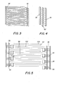
- a four phase grid structure such as the array 72 may comprise, as disclosed in Figure 3, two two-phase integrated electrode arrays 84 and 86, respectively etched on opposite sides of a thin metal clad foil.
- the two-phase patterns are identical and made from the same master.
- the pattern on the one side is displaced vertically, i.e. perpendicular to the lines, a half of the center-to-center distance between the lines on one side.
- the same pattern, on the opposite side is also shown displaced horizonally. However, this is optional. This displacement minimizes the interelectrode capacitance and reduces the possibility of electrical short circuits.
- a grid structure of the type shown in Figure 3 may be made by using phototgols 88 and 90 ( Figure 4) which form respectively the back and front patterns thereof. These phototools have interdigited arrays facing each other. Phototools can be precisely matched, displaced and pinned. A foil 92 with a metal and photoresist on both sides thereof may be interposed between phototools. The phototools are pressed together and then exposed. Subsequent development and etching completes the formation of the grid depicted in Figure 2. If desirable, contact pads can be incorporated in the phototools or may be added later by metal evaporation.
- Figure 5 depicts another type of grid structure that can be readily fabricated.
- all four electrodes patterns are coplanar.
- the circuit can be photofabricated using a single mask.
- electrodes 94 and 96 are connected only to pads which have to be interconnected. These interconnections can be constructed by metal evaporation through a shadow mask, indicated by reference numeral 98, by wire bonding, or by metal deposition through holes in the photoresist layer. Wire 100 and wire 102 are also connected to the appropriate pads. All the photoresist layers are aligned with the pads for electrodes 94 and 96. The advantage of this latter technique is that the alignment of the interconnections requires only one-fourth the precision required for the grid lines compared to the embodiment of Figure 2.
- the voltage source 82 is connected to the electrodes such that each phase thereof is connected to every fourth electrode. Each successive voltage phase is 90 degrees out of phase with the next phase, either advanced or retarded, depending on the desired direction of toner movement.
- the voltage source 82 forms part of a control circuit generally indicated by reference character 83.
- the circuit also comprises a phase shifting components indicated in block form by reference character 120.
- the phase shifting circuit may comprise a plurality of operational amplifiers and associated circuitry, not shown which serve to produce four phase shifted outputs 122, 124, 126 and 128. Each of the outputs is operatively connected to a primary winding of a transformer, for example, winding 130 via an audio amplifier, for example, amplifier 132.
- the secondary 134 of the transformer is connected to the electrode 94.
- phase shifting circuitry is connected to the electrodes 96, 100 and 102.
- a typical width for each of the electrodes is 25 to 125 lim.
- Typical spacing between the centers of the electrodes is twice the electrode width and the spacing between adjacent electrodes is approximately the same as the electrode width.
- Typical operating frequency is between 1000 and 10,000 Hz for 5 lines per mm grids (100 ⁇ m electrodes), the drive frequency for maximum transport rate being 2,000 Hz.
- the electrodes may be exposed metal such as Cu or Al it is preferred that they be covered or overcoated with a thin oxide or insulator layer.
- a thin coating having a thickness of about half the electrode width will sufficiently attenuate the higher harmonic frequencies and suppress attraction to the electrode edges by polarization forces.
- a slightly conductive overcoating will allow for the relaxation of charge accumulation due to charge exchange with the toner.
- a thin coating of a material which is non-tribo active with respect to the toner is desirable.
- a weakly tribo-active material which maintains the desired charge level may also be utilized.
- a preferred covercoating layer comprises a strongly injecting active matrix such as that disclosed in our European Patent Application No. 84 308 867.5.
- the layer comprises an insulating film forming continuous phase comprising charge transport molecules and finely divided charge injection enabling particles dispersed in the continuous phase.
- a polyvinylfluoride film available from the E. I. duPont de Nemours and Company under the tradename Tedlar has also been found to be suitable for use as the overcoat.
- a toner conveyor which is capable of transporting toner from a supply thereof to an imaging surface which may comprise a charge-retentive surface without creating large adhesion forces between the toner particles and the conveyor.
- the electrostatic forces forming the latent images can be substantially less than those of prior art devices in order to effect transfer of the toner particles from the conveyor to the images resulting in a development system that is more sensitive than those of the prior art thereby allowing for the formation of latent electrostatic images with lower contrast voltages.
Abstract
Description
- This invention relates to printing machines, and more particularly, to a toner conveyor for transporting toner from a supply to a development station where the toner is used to form powder images on substrates positioned at the development station.
- By way of example, the present invention will be disclosed in connection with a machine wherein the well known xerographic process is utilized. The invention as will be appreciated is however not limited to such environments. In the art of xerography or other similar image reproducing arts, a latent electrostatic image is formed on a charge-retentive surface such as a photoconductor which generally comprises a photoconductive insulating material adhered to a conductive backing. The photoconductor is first provided with a uniform charge after which it is exposed to a light image of an original document to be reproduced. The latent electrostatic images, thus formed, are rendered visible by applying any one of numerous pigmented resins specifically designed for this purpose. In the case of a reusable photoconductive surface, the pigmented resin, more commonly referred to as toner which forms the visible images, is transferred to plain paper.
- It should be understood that for the purposes of the present invention, which relates to transporting toner to a development station for the purpose of forming powder images thereat, the latent electrostatic images discussed above may be formed by means other than by the exposure of an electrostatically charged photosensitive member to a light image of an original document. For example, the latent electrostatic image may be generated from Information electronically stored or generated, and the digital information may be converted to alphanumeric images by image generation electronics and optics. However, such electronic and optic devices form no part of the present invention. Moreover, while the present invention is herein disclosed in connection with images formed xerographically the formation of the images on non- charged plain paper is also contemplated.
- In the application of the toner to the latent electrostatic images contained on the charge-retentive surface, it is'necessary to transport the toner from a developer housing to the surface. A basic limitation of conventional xerographic development systems, including both magnetic brush and single component, is the inability to deliver toner (i.e. charged pigment) to the latent images without creating large adhesive forces between the toner and the conveyor which transport the toner to latent images. As will be appreciated, large fluctuations (i.e. noise) in the adhesive forces that cause the pigment to tenaciously adhere to the carrier severely limit the sensitivity of the developer system thereby necessitating higher contrast voltages forming the images. Accordingly, it is desirable to reduce such noise particularly in connection with latent images formed by contrasting voltages.
- The present invention is intended to minimize the creation of such fluctuation in adhesive forces, and provides a toner transport apparatus which is characterised in that the array comprises a plurality of spaced apart linear electrodes extending across the width of said base member, and in that a source of a.c. multi-phase voltage is operatively connected to said electrode array, the phases applied to successive electrodes being shifted with respect to each other such as to create a travelling electrostatic wave pattern capable of moving toner particles along the base member from said supply to said imaging surface. In this apparatus, the travelling electrostatic wave pattern can move the toner about the surface of the conveyor with minimal contact therewith.
- The travelling wave is generated by alternating voltages of three or more phases applied to a linear array of conductors placed about the outer periphery of the conveyor. The force F for moving the toner about the conveyor is equal QEt where Q is the charge on the toner and Et is the tangential field supplied by a multi-phase a.c. voltage applied to the array of conductors. Toner is presented to the conveyor by means of a magnetic brush which is rotated in the same direction as the travelling wave. As will be apparent, other methods could be employed. This gives an initial velocity to the toner particles which enables toner having a much lower charge to be propelled by the wave.
- Travelling waves have been employed for transporting particulate material, for example, U.S. Patent 3,872,361 issued to Masuda discloses an apparatus in which the flow of particulate material along a defined path is controlled electrodynamically by means of elongated electrodes curved concentrically to a path, as axially spaced rings or interwound spirals. Each electrode is axially spaced from its neighbors by a distance about equal to its diameter and is connected with one terminal of a multi-phase alternating high voltage source. Adjacent electrodes along the path are connected with different terminals in a regular sequence, producing a wave-like, non-uniform electric field that repels electrically charged particles axially inwardly and tends to propel them along the path.
- U.S. Patent 3,778,678 also issued to Masuda relates to a similar device as that disclosed in the aforementioned '361 patent.
- U.S. Patent 3,801,869 issued to Masuda discloses a booth in which electrically charged particulate material is sprayed onto a workpiece having an opposite charge, so that the particles are electrostatically attracted to the workpiece. All of the walls that confront the workpiece are made of electrically insulating material. A grid-like arrangement of parallel, spaced apart electrodes, insulated from each other extends across the entire area of every wall, parallel to a surface of the wall and in intimate juxtaposition thereto. Each electrode is connected with one terminal of an alternating high voltage source, every electrode with a different terminal than each of the electrodes laterally adjacent to it, to produce a constantly varying field that electrodynamically repels particles from the wall. While the primary purpose of the device disclosed is for powder painting, it is contended therein that it can be used for electrostatic printing.
- The Masuda devices all utilize a relatively high voltage source (i.e. 5-10KV) operated at a relatively low frequency, i.e. 50Hz, for generating his travelling waves. In a confined area such as a tube or between parallel plates the use of high voltages is tolerable and in the case of the '869 patent even necessary since a high voltage is required to charge the initally uncharged particles.
- The movement of toner for use in a xerographic development system is also known, as disclosed in FX/4072 (Fuji Xerox's Japanese patent application) filed in Japan on May 7, 1981. In that application, there is disclosed a device comprising an elongated conduit which utilizes travelling waves for transporting toner from a supply bottle to a toner hopper.
- The apparatus of the present invention, in contrast to the devices described above uses a conveyor having a linear electrode array disposed adjacent the outer surface thereof. The electrodes forming the array are coextensive with the longitudinal axis of the conveyor and they are connected to a relatively low voltage (i.e. 30-1000 volts) source operated at a relatively higher frequency, for example, 1000 Hz. The toner transported by the conveyor to the image receiving surface is moved about the circumference thereof from the toner supply to the area of the surface, movement being caused by the travelling electrostatic waves generated by the electrode array. The toner particles are continuously scattered off the surface of the grid so that they bounce along making a miniature cloud of toner which extends above the surface approximately one wavelength. In the direction of motion, the clouds are about 1/8 to 1/4 of a wavelength long, so the clouds are actually tall and thin. Only the particles closer to the surface actually collide with the surface.
- Other aspects of the present invention will become apparent as the following description proceeds with reference to the drawings wherein:
- Figure 1 is a schematic elevational view depicting an electrophotographic printing machine incorporating the present invention.
- Figure 2 is a schematic illustration of a travelling wave conveyor system used in the machine of Figure 1;
- Figure 3 is a schematic plan view of a grid structure used in the conveyor system of Figure 2;
- Figure 4 is a schematic plan view of phototools used for fabricating the grid structure of Figure 3 with a foil disposed therebetween;
- Figure 5 is an alternative embodiment of the grid structure used in Figure 3; and
- Figure 6 is a schematic illustration of a multi-phase voltage circuit for energizing the electrodes of the travelling wave conveyor system of the invention.
- Inasmuch as the art of electrophotographic printing is well known, the various processing stations employed in the printing machine illustrated in Figure 1 will be described only briefly.
- As shown in Figure 1, the printing machine utilizes a
photoconductive belt 10 which consists of an electrically conductive substrate 11, acharge generator layer 12 comprising photoconductive particles raodomly dispersed in an electrically insulating organic resin and acharge transport layer 14 comprising a transparent electrically inactive polycarbonate resin having dissolved therein one or more diamines. A photoconductive belt of the foregoing type belt is disclosed in U.S. Patent No. 4,265,990 issued May 5, 1981 in the name of Milan Stolka et al. Belt 10 moves in the direction ofarrow 16 to advance successive portions thereof sequentially through the various processing stations disposed about the path of movement thereof. -
Belt 10 is entrained aboutstripping roller 18,tension roller 20 anddrive roller 22.Roller 22 is coupled tomotor 24 by suitable means such as a drive chain. -
Belt 10 is maintained in tension by a pair of springs (not shown) which resiliently urgetension roller 20 againstbelt 10 with the desired spring force. Bothstripping roller 18 andtension roller 20 are rotatably mounted. These rollers are idlers which rotate freeely asbelt 10 moves in the direction ofarrow 16. - With continued reference to Figure 1, initially a portion of
belt 10 passes through charging station A. At charging station A, a corona device indicated generally byreference numeral 25 charges thelayer 12 ofbelt 10 to a relatively high, substantially uniform negative potential. - A suitable corona generating device for negatively charging the
photoconductive belt 10 comprises aconductive shield 26 andcorona wire 27, the latter of which is coated with an electrically insulatinglayer 28 having a thickness which precludes a net d.c. corona current when an a.c. voltage is applied to the corona wire when the shield and photoconductive surface are at the same potential. - Next, the charged portion of the photoconductive belt is advanced through exposure station B. At exposure station B, an
original document 30 is positioned face down upon atransparent platen 32 and illuminated bylamps 34. The light rays reflected fromoriginal document 30 form images which are transmitted throughlens 36. The light images are projected onto the charged portion of the photoconductive belt to selectively dissipate the charge thereon. This records an electrostatic latent image on the belt which corresponds to the informational area contained withinoriginal document 30. - Thereafter, belt 10 advances the electrostatic latent image to development station C. At development station C, a travelling
wave conveyor 38 advances non-insulative toner particles into contact with the electrostatic latent images formed on thephotoconductive belt 10. The latent images attract the toner particles from the charged toner conveyor thereby forming toner images on the photoconductive belt. -
Belt 10 then advances the toner powder image to transfer station D. At transfer station D, a sheet ofsupport material 40 is moved into contact with the toner powder images. The sheet of support material is advanced to transfer station D by asheet feeding apparatus 42. Preferably,sheet feeding apparatus 42 includes afeed roll 44 contacting the upper sheet ofstack 46.Feed roll 44 rotates so as to advance the upper most sheet fromstack 46 intochute 48.Chute 48 directs the advancing sheet of support material into contact with thebelt 10 in a timed sequence so that the toner powder image developed thereon contacts the advancing sheet of support material at transfer station D. - Transfer station D Includes a
corona generating device 50 which sprays ions of a suitable polarity onto the backside ofsheet 40 so that the toner powder images are attracted fromphotoconductive belt 10 tosheet 40. After transfer, the sheet continues to move in the direction ofarrow 52 onto a conveyor (not shown) which advances the sheet to fusing station E. - Fusing station E includes a fuser assembly, indicated generally by the
reference numeral 54, which permanently affixes the transferred toner powder images tosheet 40. Preferably,fuser assembly 54 includes aheated fuser roller 56 adapted to be pressure engaged with abackup roller 58 with the toner powder images contactingfuser roller 56. In this manner, the toner powder images are permanently affixed tosheet 40. After fusing,chute 60 guides the advancingsheet 40 to catchtray 62 for removal from the printing machine by the operator. - Any toner particles remaining on the
belt 10 after transfer of the developed image are cleaned from the belt at cleaning station F, which includes apre-clean corotron 63. - The travelling
wave conveyor 38 comprises, as illustrated in Figure 2, abase member 70 on which there is carried a linear electrode array generally indicated byreference numeral 72. Thebase member 70 preferably has a generally cylindrical shape. The conveyor is adapted to transport the toner particles clockwise about the periphery thereof in a manner to be discussed hereinbelow. Of course, the particles could also be moved in the opposite direction. The toner particles are delivered to the conveyor via amagnetic brush 76 which is mounted for rotation in the direction of the arrow in adeveloper housing 78 containingtoner particles 80. The brush is adapted to be rotated by a drive (not shown) in the same direction as the travelling wave to thereby deposit toner on the conveyor. The travelling waves then carry the toner about the surface of the conveyor. Avacuum device 81 is provided for removing non-transferred toner. - The
electrode array 72 preferably comprises a four-phase gridstructure comprising electrodes belt 10 where they are transferred to the latent electrostatic images on the belt due to the attraction of the image field on the belt. - A four phase grid structure such as the
array 72 may comprise, as disclosed in Figure 3, two two-phase integratedelectrode arrays - A grid structure of the type shown in Figure 3, may be made by using phototgols 88 and 90 (Figure 4) which form respectively the back and front patterns thereof. These phototools have interdigited arrays facing each other. Phototools can be precisely matched, displaced and pinned. A
foil 92 with a metal and photoresist on both sides thereof may be interposed between phototools. The phototools are pressed together and then exposed. Subsequent development and etching completes the formation of the grid depicted in Figure 2. If desirable, contact pads can be incorporated in the phototools or may be added later by metal evaporation. - Figure 5 depicts another type of grid structure that can be readily fabricated. In this case, all four electrodes patterns are coplanar. The circuit can be photofabricated using a single mask. However,
electrodes reference numeral 98, by wire bonding, or by metal deposition through holes in the photoresist layer.Wire 100 andwire 102 are also connected to the appropriate pads. All the photoresist layers are aligned with the pads forelectrodes - As illustrated in Figure 6, the
voltage source 82 is connected to the electrodes such that each phase thereof is connected to every fourth electrode. Each successive voltage phase is 90 degrees out of phase with the next phase, either advanced or retarded, depending on the desired direction of toner movement. Thevoltage source 82 forms part of a control circuit generally indicated byreference character 83. The circuit also comprises a phase shifting components indicated in block form byreference character 120. The phase shifting circuit may comprise a plurality of operational amplifiers and associated circuitry, not shown which serve to produce four phase shiftedoutputs amplifier 132. The secondary 134 of the transformer is connected to theelectrode 94. Similarly, phase shifting circuitry is connected to theelectrodes - A typical width for each of the electrodes is 25 to 125 lim. Typical spacing between the centers of the electrodes is twice the electrode width and the spacing between adjacent electrodes is approximately the same as the electrode width. Typical operating frequency is between 1000 and 10,000 Hz for 5 lines per mm grids (100 µm electrodes), the drive frequency for maximum transport rate being 2,000 Hz.
- While the electrodes may be exposed metal such as Cu or Al it is preferred that they be covered or overcoated with a thin oxide or insulator layer. A thin coating having a thickness of about half the electrode width will sufficiently attenuate the higher harmonic frequencies and suppress attraction to the electrode edges by polarization forces. A slightly conductive overcoating will allow for the relaxation of charge accumulation due to charge exchange with the toner. To avoid excessive alteration of the toner charge as it moves about the conveyor, however, a thin coating of a material which is non-tribo active with respect to the toner is desirable. A weakly tribo-active material which maintains the desired charge level may also be utilized.
- A preferred covercoating layer comprises a strongly injecting active matrix such as that disclosed in our European Patent Application No. 84 308 867.5. As disclosed therein, the layer comprises an insulating film forming continuous phase comprising charge transport molecules and finely divided charge injection enabling particles dispersed in the continuous phase. A polyvinylfluoride film available from the E. I. duPont de Nemours and Company under the tradename Tedlar has also been found to be suitable for use as the overcoat.
- As can now be appreciated, there has been disclosed a toner conveyor which is capable of transporting toner from a supply thereof to an imaging surface which may comprise a charge-retentive surface without creating large adhesion forces between the toner particles and the conveyor. In the case of xerographically formed images, the electrostatic forces forming the latent images can be substantially less than those of prior art devices in order to effect transfer of the toner particles from the conveyor to the images resulting in a development system that is more sensitive than those of the prior art thereby allowing for the formation of latent electrostatic images with lower contrast voltages.
Claims (10)
Applications Claiming Priority (2)
| Application Number | Priority Date | Filing Date | Title |
|---|---|---|---|
| US06/614,499 US4647179A (en) | 1984-05-29 | 1984-05-29 | Development apparatus |
| US614499 | 1984-05-29 |
Publications (3)
| Publication Number | Publication Date |
|---|---|
| EP0163484A2 true EP0163484A2 (en) | 1985-12-04 |
| EP0163484A3 EP0163484A3 (en) | 1987-08-19 |
| EP0163484B1 EP0163484B1 (en) | 1990-03-21 |
Family
ID=24461505
Family Applications (1)
| Application Number | Title | Priority Date | Filing Date |
|---|---|---|---|
| EP85303617A Expired - Lifetime EP0163484B1 (en) | 1984-05-29 | 1985-05-22 | Development apparatus |
Country Status (4)
| Country | Link |
|---|---|
| US (1) | US4647179A (en) |
| EP (1) | EP0163484B1 (en) |
| JP (1) | JPS60257461A (en) |
| DE (1) | DE3576747D1 (en) |
Cited By (1)
| Publication number | Priority date | Publication date | Assignee | Title |
|---|---|---|---|---|
| EP0334581A2 (en) * | 1988-03-21 | 1989-09-27 | Xerox Corporation | Apparatus for developing latent electrostatic images |
Families Citing this family (73)
| Publication number | Priority date | Publication date | Assignee | Title |
|---|---|---|---|---|
| JPS6313059A (en) * | 1986-07-03 | 1988-01-20 | Canon Inc | Developing method |
| US4780733A (en) * | 1987-12-31 | 1988-10-25 | Xerox Corporation | Printing apparatus and toner/developer delivery system therefor |
| US4876561A (en) * | 1988-05-31 | 1989-10-24 | Xerox Corporation | Printing apparatus and toner/developer delivery system therefor |
| US4875081A (en) * | 1988-10-24 | 1989-10-17 | Xerox Corporation | Electrophotographic device having a.c. biased cleaning member |
| US4912489A (en) * | 1988-12-27 | 1990-03-27 | Xerox Corporation | Direct electrostatic printing apparatus with toner supply-side control electrodes |
| US4903050A (en) * | 1989-07-03 | 1990-02-20 | Xerox Corporation | Toner recovery for DEP cleaning process |
| US4949103A (en) * | 1989-08-28 | 1990-08-14 | Xerox Corporation | Direct electrostatic printing apparatus and method for making labels |
| US5210551A (en) * | 1990-06-18 | 1993-05-11 | Casio Computer Co., Ltd. | Electrostatic recording apparatus with an electrode drive means within the developer circulating path |
| US5204697A (en) * | 1990-09-04 | 1993-04-20 | Xerox Corporation | Ionographic functional color printer based on Traveling Cloud Development |
| US5095322A (en) * | 1990-10-11 | 1992-03-10 | Xerox Corporation | Avoidance of DEP wrong sign toner hole clogging by out of phase shield bias |
| US5504563A (en) * | 1991-07-01 | 1996-04-02 | Xerox Corporation | Scavengeless donor roll development |
| US5416568A (en) * | 1991-07-09 | 1995-05-16 | Ricoh Company, Ltd. | Developing unit for an image forming apparatus |
| JP3154434B2 (en) * | 1991-10-04 | 2001-04-09 | 株式会社リコー | Image forming method and image forming apparatus |
| US5281982A (en) * | 1991-11-04 | 1994-01-25 | Eastman Kodak Company | Pixelized toning |
| US5204696A (en) * | 1991-12-16 | 1993-04-20 | Xerox Corporation | Ceramic printhead for direct electrostatic printing |
| US5621506A (en) * | 1993-03-12 | 1997-04-15 | Kabushiki Kaisha Toshiba | Electrostatic recording apparatus providing an electric field adjacent a developer roller |
| US5289240A (en) * | 1993-05-20 | 1994-02-22 | Xerox Corporation | Scavengeless developer unit with electroded donor roll |
| US5360940A (en) * | 1993-07-14 | 1994-11-01 | Xerox Corporation | Scavengeless two component development with an electroded development roll |
| US5394225A (en) * | 1993-11-23 | 1995-02-28 | Xerox Corporation | Optical switching scheme for SCD donor roll bias |
| BE1008460A4 (en) * | 1994-06-15 | 1996-05-07 | Agfa Gevaert Nv | TRANSPORTATION DEVICE FOR MAGNETISABLE PARTICLES. |
| US5539501A (en) * | 1995-07-20 | 1996-07-23 | Xerox Corporation | High slope AC charging device having groups of wires |
| US5893015A (en) * | 1996-06-24 | 1999-04-06 | Xerox Corporation | Flexible donor belt employing a DC traveling wave |
| US5717986A (en) * | 1996-06-24 | 1998-02-10 | Xerox Corporation | Flexible donor belt |
| US5767877A (en) * | 1996-08-13 | 1998-06-16 | Xerox Corporation | Toner jet printer |
| US5701564A (en) * | 1996-09-26 | 1997-12-23 | Xerox Corporation | Scavengeless development apparatus including an electroded donor roll having a tri-contact commutator assembly |
| US5889541A (en) * | 1996-10-09 | 1999-03-30 | Xerox Corporation | Two-dimensional print cell array apparatus and method for delivery of toner for printing images |
| US5809385A (en) * | 1997-06-30 | 1998-09-15 | Xerox Corporation | Reproduction machine including and acoustic scavengeless assist development apparatus |
| US6309049B1 (en) | 1998-02-18 | 2001-10-30 | The Salmon Group Llc | Printing apparatus and method for imaging charged toner particles using direct writing methods |
| US5850587A (en) * | 1998-04-01 | 1998-12-15 | Schmidlin; Fred W. | Electrostatic toner conditioning and controlling means II |
| US6467862B1 (en) | 1998-09-30 | 2002-10-22 | Xerox Corporation | Cartridge for use in a ballistic aerosol marking apparatus |
| US6416157B1 (en) | 1998-09-30 | 2002-07-09 | Xerox Corporation | Method of marking a substrate employing a ballistic aerosol marking apparatus |
| US6290342B1 (en) | 1998-09-30 | 2001-09-18 | Xerox Corporation | Particulate marking material transport apparatus utilizing traveling electrostatic waves |
| US6136442A (en) * | 1998-09-30 | 2000-10-24 | Xerox Corporation | Multi-layer organic overcoat for particulate transport electrode grid |
| US6265050B1 (en) | 1998-09-30 | 2001-07-24 | Xerox Corporation | Organic overcoat for electrode grid |
| US6523928B2 (en) | 1998-09-30 | 2003-02-25 | Xerox Corporation | Method of treating a substrate employing a ballistic aerosol marking apparatus |
| US6416156B1 (en) | 1998-09-30 | 2002-07-09 | Xerox Corporation | Kinetic fusing of a marking material |
| US6454384B1 (en) | 1998-09-30 | 2002-09-24 | Xerox Corporation | Method for marking with a liquid material using a ballistic aerosol marking apparatus |
| US6751865B1 (en) | 1998-09-30 | 2004-06-22 | Xerox Corporation | Method of making a print head for use in a ballistic aerosol marking apparatus |
| US6511149B1 (en) | 1998-09-30 | 2003-01-28 | Xerox Corporation | Ballistic aerosol marking apparatus for marking a substrate |
| US6328409B1 (en) | 1998-09-30 | 2001-12-11 | Xerox Corporation | Ballistic aerosol making apparatus for marking with a liquid material |
| US6340216B1 (en) | 1998-09-30 | 2002-01-22 | Xerox Corporation | Ballistic aerosol marking apparatus for treating a substrate |
| US6116718A (en) * | 1998-09-30 | 2000-09-12 | Xerox Corporation | Print head for use in a ballistic aerosol marking apparatus |
| US6291088B1 (en) | 1998-09-30 | 2001-09-18 | Xerox Corporation | Inorganic overcoat for particulate transport electrode grid |
| US6035170A (en) * | 1998-12-11 | 2000-03-07 | Xerox Corporation | Reproduction machine including an electrostatic sonic toner release development apparatus |
| US6175707B1 (en) | 1999-05-17 | 2001-01-16 | Xerox Corporation | Integrated toner transport/toner charging device |
| US6293659B1 (en) | 1999-09-30 | 2001-09-25 | Xerox Corporation | Particulate source, circulation, and valving system for ballistic aerosol marking |
| US6328436B1 (en) | 1999-09-30 | 2001-12-11 | Xerox Corporation | Electro-static particulate source, circulation, and valving system for ballistic aerosol marking |
| US6104904A (en) * | 1999-10-04 | 2000-08-15 | Xerox Corporation | Reproduction machine including a pneumatically coupled sonic toner release development apparatus |
| US6205313B1 (en) | 1999-11-23 | 2001-03-20 | Xerox Corporation | Toner charging system for atom imaging process |
| US6137979A (en) * | 1999-12-10 | 2000-10-24 | Xerox Corporation | Toner transport using superimposed traveling electric potential waves |
| US6272296B1 (en) | 1999-12-10 | 2001-08-07 | Xerox Corporation | Method and apparatus using traveling wave potential waveforms for separation of opposite sign charge particles |
| US6219515B1 (en) | 1999-12-17 | 2001-04-17 | Xerox Corporation | Vibrating travel wave grid |
| US6246855B1 (en) | 2000-05-30 | 2001-06-12 | Xerox Corporation | Apparatus for loading dry xerographic toner onto a traveling wave grid |
| WO2002036464A1 (en) | 2000-11-03 | 2002-05-10 | Technology Innovations, Llc | Powder conveying and dispensing method and apparatus using traveling wave transport |
| US6351623B1 (en) | 2000-11-27 | 2002-02-26 | Xerox Corporation | Toner dispensing apparatus employing a traveling wave transport grid |
| US6477351B1 (en) | 2000-11-27 | 2002-11-05 | Xerox Corporation | Blade cleaning system employing an electrode array |
| JP3626119B2 (en) * | 2001-06-27 | 2005-03-02 | シャープ株式会社 | Developing device and image forming apparatus having the same |
| US6634095B2 (en) * | 2001-06-27 | 2003-10-21 | International Business Machines Corporation | Apparatus for mounting a land grid array module |
| US6911593B2 (en) * | 2002-09-24 | 2005-06-28 | Board Of Trustees Of The University Of Arkansas | Transparent self-cleaning dust shield |
| US7150813B2 (en) * | 2003-06-12 | 2006-12-19 | Palo Alto Research Center Incorporated | Isoelectric focusing (IEF) of proteins with sequential and oppositely directed traveling waves in gel electrophoresis |
| US7282129B2 (en) * | 2003-06-12 | 2007-10-16 | Palo Alto Research Center Incorporated | Traveling wave algorithms to focus and concentrate proteins in gel electrophoresis |
| US7156970B2 (en) * | 2003-06-12 | 2007-01-02 | Palo Alto Research Center Incorporated | Distributed multi-segmented reconfigurable traveling wave grids for separation of proteins in gel electrophoresis |
| US7217901B2 (en) * | 2003-07-02 | 2007-05-15 | Xerox Corporation | System for transporting and selectively sorting particles and method of using the same |
| US6969160B2 (en) * | 2003-07-28 | 2005-11-29 | Xerox Corporation | Ballistic aerosol marking apparatus |
| US7163611B2 (en) * | 2003-12-03 | 2007-01-16 | Palo Alto Research Center Incorporated | Concentration and focusing of bio-agents and micron-sized particles using traveling wave grids |
| US7309410B2 (en) | 2003-12-03 | 2007-12-18 | Palo Alto Research Center Incorporated | Traveling wave grids and algorithms for biomolecule separation, transport and focusing |
| US7293862B2 (en) * | 2004-10-29 | 2007-11-13 | Xerox Corporation | Reservoir systems for administering multiple populations of particles |
| US7235123B1 (en) * | 2004-10-29 | 2007-06-26 | Palo Alto Research Center Incorporated | Particle transport and near field analytical detection |
| US7695602B2 (en) * | 2004-11-12 | 2010-04-13 | Xerox Corporation | Systems and methods for transporting particles |
| US8020975B2 (en) * | 2004-12-03 | 2011-09-20 | Xerox Corporation | Continuous particle transport and reservoir system |
| DE102004059532A1 (en) * | 2004-12-09 | 2006-06-14 | OCé PRINTING SYSTEMS GMBH | Electrographic printing or copying device and method for operating the printing or copying device |
| US7681738B2 (en) * | 2005-09-12 | 2010-03-23 | Palo Alto Research Center Incorporated | Traveling wave arrays, separation methods, and purification cells |
| CN104588369A (en) * | 2013-11-01 | 2015-05-06 | 上海空间电源研究所 | Dust collection device of spiral electric curtain |
Citations (6)
| Publication number | Priority date | Publication date | Assignee | Title |
|---|---|---|---|---|
| US4017648A (en) * | 1975-02-03 | 1977-04-12 | Xerox Corporation | Toner agitation through microfield donor |
| US4282303A (en) * | 1980-05-05 | 1981-08-04 | Xerox Corporation | Development method and apparatus |
| US4289837A (en) * | 1980-05-05 | 1981-09-15 | Xerox Corporation | Development method and apparatus |
| JPS597972A (en) * | 1982-07-06 | 1984-01-17 | Toshiba Corp | Developing device |
| EP0106322A1 (en) * | 1982-10-15 | 1984-04-25 | Kabushiki Kaisha Toshiba | Developing apparatus |
| JPS5979266A (en) * | 1982-10-29 | 1984-05-08 | Toshiba Corp | Developing device |
Family Cites Families (12)
| Publication number | Priority date | Publication date | Assignee | Title |
|---|---|---|---|---|
| US3113042A (en) * | 1960-04-19 | 1963-12-03 | Xerox Corp | Xerographic apparatus with magnetic conveyor |
| BE789579A (en) * | 1971-10-06 | 1973-02-01 | Masuda Senichi | ENCLOSURE FOR THE APPLICATION, BY MEANS OF A CURTAIN OF ELECTRICAL FIELDS OF THE CONTACT TYPE, OF COATINGS FORMED BY ELECTROSTATIC CHARGED POWDERS |
| US3778678A (en) * | 1972-02-16 | 1973-12-11 | S Masuda | Apparatus for electric field curtain of contact type |
| US3872361A (en) * | 1973-06-04 | 1975-03-18 | Senichi Masuda | Electrodynamic apparatus for controlling flow of particulate material |
| US4265990A (en) * | 1977-05-04 | 1981-05-05 | Xerox Corporation | Imaging system with a diamine charge transport material in a polycarbonate resin |
| DE3138507C2 (en) * | 1981-09-28 | 1983-08-18 | Siemens AG, 1000 Berlin und 8000 München | Device for developing an electrostatic charge image with toner particles |
| JPS59126556A (en) * | 1983-01-10 | 1984-07-21 | Fuji Xerox Co Ltd | Protecting device of electric field curtain device |
| JPS59181374A (en) * | 1983-03-31 | 1984-10-15 | Toshiba Corp | Developing device |
| JPS59181375A (en) * | 1983-03-31 | 1984-10-15 | Toshiba Corp | Developing device |
| JPS59181371A (en) * | 1983-03-31 | 1984-10-15 | Toshiba Corp | Developing device |
| JPS59189371A (en) * | 1983-04-12 | 1984-10-26 | Toshiba Corp | Developing device |
| JPS59189372A (en) * | 1983-04-13 | 1984-10-26 | Toshiba Corp | Developing device |
-
1984
- 1984-05-29 US US06/614,499 patent/US4647179A/en not_active Expired - Lifetime
-
1985
- 1985-05-22 JP JP60110070A patent/JPS60257461A/en active Pending
- 1985-05-22 DE DE8585303617T patent/DE3576747D1/en not_active Expired - Fee Related
- 1985-05-22 EP EP85303617A patent/EP0163484B1/en not_active Expired - Lifetime
Patent Citations (6)
| Publication number | Priority date | Publication date | Assignee | Title |
|---|---|---|---|---|
| US4017648A (en) * | 1975-02-03 | 1977-04-12 | Xerox Corporation | Toner agitation through microfield donor |
| US4282303A (en) * | 1980-05-05 | 1981-08-04 | Xerox Corporation | Development method and apparatus |
| US4289837A (en) * | 1980-05-05 | 1981-09-15 | Xerox Corporation | Development method and apparatus |
| JPS597972A (en) * | 1982-07-06 | 1984-01-17 | Toshiba Corp | Developing device |
| EP0106322A1 (en) * | 1982-10-15 | 1984-04-25 | Kabushiki Kaisha Toshiba | Developing apparatus |
| JPS5979266A (en) * | 1982-10-29 | 1984-05-08 | Toshiba Corp | Developing device |
Non-Patent Citations (1)
| Title |
|---|
| PATENT ABSTRACTS OF JAPAN, vol. 8, no. 92 (P-271)[1529], 27th April 1984; & JP-A-59 007 972 (TOKYO SHIBAURA DENKI K.K.) 17-01-1984 * |
Cited By (2)
| Publication number | Priority date | Publication date | Assignee | Title |
|---|---|---|---|---|
| EP0334581A2 (en) * | 1988-03-21 | 1989-09-27 | Xerox Corporation | Apparatus for developing latent electrostatic images |
| EP0334581A3 (en) * | 1988-03-21 | 1991-03-13 | Xerox Corporation | Apparatus for developing latent electrostatic images |
Also Published As
| Publication number | Publication date |
|---|---|
| US4647179A (en) | 1987-03-03 |
| DE3576747D1 (en) | 1990-04-26 |
| JPS60257461A (en) | 1985-12-19 |
| EP0163484A3 (en) | 1987-08-19 |
| EP0163484B1 (en) | 1990-03-21 |
Similar Documents
| Publication | Publication Date | Title |
|---|---|---|
| EP0163484B1 (en) | Development apparatus | |
| US5893015A (en) | Flexible donor belt employing a DC traveling wave | |
| US5717986A (en) | Flexible donor belt | |
| US4876575A (en) | Printing apparatus including apparatus and method for charging and metering toner particles | |
| US4282303A (en) | Development method and apparatus | |
| EP0274895B1 (en) | Corona charging device | |
| EP0533347B1 (en) | Development system | |
| US4289837A (en) | Development method and apparatus | |
| JPH07199642A (en) | Donor structure | |
| US5413807A (en) | Method of manufacturing a donor roll | |
| EP0435566B1 (en) | Electrostatographic apparatus | |
| US6175707B1 (en) | Integrated toner transport/toner charging device | |
| EP0532306B1 (en) | A system for removing agglomerates from a developed image on a photoreceptor | |
| EP0147187B1 (en) | Cleaning apparatus for charge retentive surface | |
| US5600418A (en) | Donor rolls with exterior commutation | |
| EP0120688B1 (en) | A development system using a thin layer of marking particles | |
| US4615613A (en) | Charge particle removal device | |
| EP0036290B1 (en) | Apparatus for cleaning particles from a surface | |
| US5504563A (en) | Scavengeless donor roll development | |
| US4752810A (en) | Cleaning apparatus for charge retentive surfaces | |
| CA1103740A (en) | Transfer of conductive particles | |
| US4727823A (en) | Magnetic roll structure for transporting single component magnetic developer | |
| US5729807A (en) | Optically switched commutator scheme for hybrid scavengeless segmented electroded donor rolls | |
| EP0741339B1 (en) | Modular charging device for imaging system | |
| JPH05188773A (en) | Developing device |
Legal Events
| Date | Code | Title | Description |
|---|---|---|---|
| PUAI | Public reference made under article 153(3) epc to a published international application that has entered the european phase |
Free format text: ORIGINAL CODE: 0009012 |
|
| AK | Designated contracting states |
Designated state(s): DE FR GB |
|
| PUAL | Search report despatched |
Free format text: ORIGINAL CODE: 0009013 |
|
| AK | Designated contracting states |
Kind code of ref document: A3 Designated state(s): DE FR GB |
|
| 17P | Request for examination filed |
Effective date: 19880218 |
|
| 17Q | First examination report despatched |
Effective date: 19880429 |
|
| GRAA | (expected) grant |
Free format text: ORIGINAL CODE: 0009210 |
|
| AK | Designated contracting states |
Kind code of ref document: B1 Designated state(s): DE FR GB |
|
| REF | Corresponds to: |
Ref document number: 3576747 Country of ref document: DE Date of ref document: 19900426 |
|
| ET | Fr: translation filed | ||
| PLBE | No opposition filed within time limit |
Free format text: ORIGINAL CODE: 0009261 |
|
| STAA | Information on the status of an ep patent application or granted ep patent |
Free format text: STATUS: NO OPPOSITION FILED WITHIN TIME LIMIT |
|
| 26N | No opposition filed | ||
| PGFP | Annual fee paid to national office [announced via postgrant information from national office to epo] |
Ref country code: FR Payment date: 20000510 Year of fee payment: 16 |
|
| PGFP | Annual fee paid to national office [announced via postgrant information from national office to epo] |
Ref country code: GB Payment date: 20000517 Year of fee payment: 16 |
|
| PGFP | Annual fee paid to national office [announced via postgrant information from national office to epo] |
Ref country code: DE Payment date: 20000522 Year of fee payment: 16 |
|
| PG25 | Lapsed in a contracting state [announced via postgrant information from national office to epo] |
Ref country code: GB Free format text: LAPSE BECAUSE OF NON-PAYMENT OF DUE FEES Effective date: 20010522 |
|
| GBPC | Gb: european patent ceased through non-payment of renewal fee |
Effective date: 20010522 |
|
| PG25 | Lapsed in a contracting state [announced via postgrant information from national office to epo] |
Ref country code: FR Free format text: LAPSE BECAUSE OF NON-PAYMENT OF DUE FEES Effective date: 20020131 |
|
| PG25 | Lapsed in a contracting state [announced via postgrant information from national office to epo] |
Ref country code: DE Free format text: LAPSE BECAUSE OF NON-PAYMENT OF DUE FEES Effective date: 20020301 |