EP0165513A2 - Semiconductor contact metal protection - Google Patents
Semiconductor contact metal protection Download PDFInfo
- Publication number
- EP0165513A2 EP0165513A2 EP85106582A EP85106582A EP0165513A2 EP 0165513 A2 EP0165513 A2 EP 0165513A2 EP 85106582 A EP85106582 A EP 85106582A EP 85106582 A EP85106582 A EP 85106582A EP 0165513 A2 EP0165513 A2 EP 0165513A2
- Authority
- EP
- European Patent Office
- Prior art keywords
- metal
- contact
- photoresist
- window
- silicon
- Prior art date
- Legal status (The legal status is an assumption and is not a legal conclusion. Google has not performed a legal analysis and makes no representation as to the accuracy of the status listed.)
- Granted
Links
- 229910052751 metal Inorganic materials 0.000 title claims abstract description 56
- 239000002184 metal Substances 0.000 title claims abstract description 56
- 239000004065 semiconductor Substances 0.000 title claims abstract description 15
- 230000004224 protection Effects 0.000 title description 4
- 229920002120 photoresistant polymer Polymers 0.000 claims abstract description 25
- 238000000034 method Methods 0.000 claims abstract description 23
- 238000000151 deposition Methods 0.000 claims abstract description 18
- 239000000126 substance Substances 0.000 claims abstract description 17
- 239000000758 substrate Substances 0.000 claims abstract description 15
- XUIMIQQOPSSXEZ-UHFFFAOYSA-N Silicon Chemical compound [Si] XUIMIQQOPSSXEZ-UHFFFAOYSA-N 0.000 claims abstract description 13
- 229910052710 silicon Inorganic materials 0.000 claims abstract description 13
- 239000010703 silicon Substances 0.000 claims abstract description 13
- 230000001681 protective effect Effects 0.000 claims abstract description 10
- 230000008021 deposition Effects 0.000 claims abstract description 5
- 239000010410 layer Substances 0.000 claims description 12
- 239000012212 insulator Substances 0.000 claims description 11
- 239000000463 material Substances 0.000 claims description 10
- 238000005530 etching Methods 0.000 claims description 4
- 239000011241 protective layer Substances 0.000 claims description 4
- RTAQQCXQSZGOHL-UHFFFAOYSA-N Titanium Chemical compound [Ti] RTAQQCXQSZGOHL-UHFFFAOYSA-N 0.000 claims description 3
- 229910052719 titanium Inorganic materials 0.000 claims description 3
- 239000010936 titanium Substances 0.000 claims description 3
- JBRZTFJDHDCESZ-UHFFFAOYSA-N AsGa Chemical compound [As]#[Ga] JBRZTFJDHDCESZ-UHFFFAOYSA-N 0.000 claims description 2
- 229910001218 Gallium arsenide Inorganic materials 0.000 claims description 2
- ZOKXTWBITQBERF-UHFFFAOYSA-N Molybdenum Chemical compound [Mo] ZOKXTWBITQBERF-UHFFFAOYSA-N 0.000 claims description 2
- 229910052782 aluminium Inorganic materials 0.000 claims description 2
- XAGFODPZIPBFFR-UHFFFAOYSA-N aluminium Chemical compound [Al] XAGFODPZIPBFFR-UHFFFAOYSA-N 0.000 claims description 2
- YXTPWUNVHCYOSP-UHFFFAOYSA-N bis($l^{2}-silanylidene)molybdenum Chemical compound [Si]=[Mo]=[Si] YXTPWUNVHCYOSP-UHFFFAOYSA-N 0.000 claims description 2
- 238000010894 electron beam technology Methods 0.000 claims description 2
- 229910052732 germanium Inorganic materials 0.000 claims description 2
- GNPVGFCGXDBREM-UHFFFAOYSA-N germanium atom Chemical compound [Ge] GNPVGFCGXDBREM-UHFFFAOYSA-N 0.000 claims description 2
- 229910052750 molybdenum Inorganic materials 0.000 claims description 2
- 239000011733 molybdenum Substances 0.000 claims description 2
- 229910021344 molybdenum silicide Inorganic materials 0.000 claims description 2
- 150000004767 nitrides Chemical class 0.000 claims description 2
- 230000003287 optical effect Effects 0.000 claims description 2
- WFKWXMTUELFFGS-UHFFFAOYSA-N tungsten Chemical compound [W] WFKWXMTUELFFGS-UHFFFAOYSA-N 0.000 claims description 2
- 229910052721 tungsten Inorganic materials 0.000 claims description 2
- 239000010937 tungsten Substances 0.000 claims description 2
- WQJQOUPTWCFRMM-UHFFFAOYSA-N tungsten disilicide Chemical compound [Si]#[W]#[Si] WQJQOUPTWCFRMM-UHFFFAOYSA-N 0.000 claims description 2
- 229910021342 tungsten silicide Inorganic materials 0.000 claims description 2
- 239000003513 alkali Substances 0.000 claims 1
- 239000011248 coating agent Substances 0.000 claims 1
- 238000000576 coating method Methods 0.000 claims 1
- 238000004519 manufacturing process Methods 0.000 claims 1
- 230000015572 biosynthetic process Effects 0.000 abstract description 4
- 239000000356 contaminant Substances 0.000 abstract description 4
- 239000011253 protective coating Substances 0.000 abstract 1
- 238000001465 metallisation Methods 0.000 description 9
- 238000001704 evaporation Methods 0.000 description 3
- 238000005755 formation reaction Methods 0.000 description 3
- 239000011800 void material Substances 0.000 description 3
- 238000006243 chemical reaction Methods 0.000 description 2
- 238000005260 corrosion Methods 0.000 description 2
- 230000007797 corrosion Effects 0.000 description 2
- 230000008020 evaporation Effects 0.000 description 2
- 239000007943 implant Substances 0.000 description 2
- 150000002739 metals Chemical class 0.000 description 2
- GPXJNWSHGFTCBW-UHFFFAOYSA-N Indium phosphide Chemical compound [In]#P GPXJNWSHGFTCBW-UHFFFAOYSA-N 0.000 description 1
- 230000004888 barrier function Effects 0.000 description 1
- 238000011109 contamination Methods 0.000 description 1
- 230000000694 effects Effects 0.000 description 1
- 230000003116 impacting effect Effects 0.000 description 1
- 238000005272 metallurgy Methods 0.000 description 1
- 238000000206 photolithography Methods 0.000 description 1
- 238000004544 sputter deposition Methods 0.000 description 1
Images


Classifications
-
- H—ELECTRICITY
- H01—ELECTRIC ELEMENTS
- H01L—SEMICONDUCTOR DEVICES NOT COVERED BY CLASS H10
- H01L23/00—Details of semiconductor or other solid state devices
- H01L23/52—Arrangements for conducting electric current within the device in operation from one component to another, i.e. interconnections, e.g. wires, lead frames
- H01L23/522—Arrangements for conducting electric current within the device in operation from one component to another, i.e. interconnections, e.g. wires, lead frames including external interconnections consisting of a multilayer structure of conductive and insulating layers inseparably formed on the semiconductor body
- H01L23/532—Arrangements for conducting electric current within the device in operation from one component to another, i.e. interconnections, e.g. wires, lead frames including external interconnections consisting of a multilayer structure of conductive and insulating layers inseparably formed on the semiconductor body characterised by the materials
- H01L23/53204—Conductive materials
- H01L23/53271—Conductive materials containing semiconductor material, e.g. polysilicon
-
- H—ELECTRICITY
- H01—ELECTRIC ELEMENTS
- H01L—SEMICONDUCTOR DEVICES NOT COVERED BY CLASS H10
- H01L21/00—Processes or apparatus adapted for the manufacture or treatment of semiconductor or solid state devices or of parts thereof
- H01L21/02—Manufacture or treatment of semiconductor devices or of parts thereof
- H01L21/027—Making masks on semiconductor bodies for further photolithographic processing not provided for in group H01L21/18 or H01L21/34
- H01L21/0271—Making masks on semiconductor bodies for further photolithographic processing not provided for in group H01L21/18 or H01L21/34 comprising organic layers
- H01L21/0272—Making masks on semiconductor bodies for further photolithographic processing not provided for in group H01L21/18 or H01L21/34 comprising organic layers for lift-off processes
-
- H—ELECTRICITY
- H01—ELECTRIC ELEMENTS
- H01L—SEMICONDUCTOR DEVICES NOT COVERED BY CLASS H10
- H01L21/00—Processes or apparatus adapted for the manufacture or treatment of semiconductor or solid state devices or of parts thereof
- H01L21/70—Manufacture or treatment of devices consisting of a plurality of solid state components formed in or on a common substrate or of parts thereof; Manufacture of integrated circuit devices or of parts thereof
- H01L21/71—Manufacture of specific parts of devices defined in group H01L21/70
- H01L21/768—Applying interconnections to be used for carrying current between separate components within a device comprising conductors and dielectrics
- H01L21/76838—Applying interconnections to be used for carrying current between separate components within a device comprising conductors and dielectrics characterised by the formation and the after-treatment of the conductors
- H01L21/76877—Filling of holes, grooves or trenches, e.g. vias, with conductive material
-
- H—ELECTRICITY
- H01—ELECTRIC ELEMENTS
- H01L—SEMICONDUCTOR DEVICES NOT COVERED BY CLASS H10
- H01L2924/00—Indexing scheme for arrangements or methods for connecting or disconnecting semiconductor or solid-state bodies as covered by H01L24/00
- H01L2924/0001—Technical content checked by a classifier
- H01L2924/0002—Not covered by any one of groups H01L24/00, H01L24/00 and H01L2224/00
-
- Y—GENERAL TAGGING OF NEW TECHNOLOGICAL DEVELOPMENTS; GENERAL TAGGING OF CROSS-SECTIONAL TECHNOLOGIES SPANNING OVER SEVERAL SECTIONS OF THE IPC; TECHNICAL SUBJECTS COVERED BY FORMER USPC CROSS-REFERENCE ART COLLECTIONS [XRACs] AND DIGESTS
- Y10—TECHNICAL SUBJECTS COVERED BY FORMER USPC
- Y10S—TECHNICAL SUBJECTS COVERED BY FORMER USPC CROSS-REFERENCE ART COLLECTIONS [XRACs] AND DIGESTS
- Y10S438/00—Semiconductor device manufacturing: process
- Y10S438/942—Masking
- Y10S438/948—Radiation resist
- Y10S438/951—Lift-off
Landscapes
- Engineering & Computer Science (AREA)
- Physics & Mathematics (AREA)
- Condensed Matter Physics & Semiconductors (AREA)
- General Physics & Mathematics (AREA)
- Computer Hardware Design (AREA)
- Microelectronics & Electronic Packaging (AREA)
- Power Engineering (AREA)
- Manufacturing & Machinery (AREA)
- Internal Circuitry In Semiconductor Integrated Circuit Devices (AREA)
- Electrodes Of Semiconductors (AREA)
Abstract
Description
- The invention disclosed broadly relates to semiconductor processing and more particularly relates to metal deposition techniques in semiconductor processing.
- Alkaline developers and chemical etchants, used to develop the photoresist layer for first and second metal layer depositions in existing FET processes, severely attack the contact metal, thereby producing poor inter level contacts and possibly electrical failures. Also, contaminant residues, or voids created by the reaction of the etchants with existing contact metals or semiconductor substrates, will impact reliability and life of the device structures. These residues and voids increase resistance which is a significant cause of device failure.
- It is known to protect ion implanted and diffused contacts by depositing a barrier metal over the implanted area so that it will not be depleted by subsequent etching and/or other processes. This provides protection for the ion implanted diffused and/or buried contacts. However, it does not protect against chemical attack on the sides of the metal contact in via holes.
- A common problem with metal deposition of contact or other metal to provide interconnections in the semiconductor device is that the state-of-the-art deposition tooling deposits metal at an angle to the device wafer surface, primarily because the molten metal source is not at a "line of sight" perpendicular to the wafer surface. Therefore voids or spacing will inherently exist between the contact metal and the sides of the etched insulator.
- It is therefore an object of the invention to provide an improved 30 metallization process for semiconductor devices.
- It is another object of the invention to provide an improved metallization process which diminishes the problem of alkaline developers attacking contact metal structures.
- It is still another object of the invention to diminish void formations and eliminate chemical residues in the metal contact area in order to maintain contact integrity.
- These and other objects, features and advantages of the invention are accomplished by the process disclosed herein. In a photoresist lift-off process for depositing metal on a semiconductor substrate, a protective layer is applied to the etched via hole prior to the metal deposition step. This prevents the formation of contaminant trapping voids and chemical residues which would otherwise occur at the base and/or sides of the metal subsequently deposited in the contact via hole. The protective layer, which has a thickness of from 10 to 30 nanometers, remains intact as a permanent part of the structure.
- These and other objects, features and advantages of the invention will be more fully appreciated with reference to the accompanying figures.
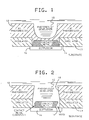
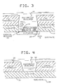
- FIGS. 1, 2 and 3 are a sequence of steps in existing photolithographic development processes, to produce a typical photoresist structure prior to metallization over contact metallurgy.
- FIG. 4 illustrates the first step of the invention relating to developing the resist of the contacts.
- FIG. 5 illustrates the steps of etching the insulator to produce contacts in the substrate and/or over the ion implanted diffused areas.
- FIG. 6 illustrates the step of flash evaporating a thin protective layer over the etched contacts and insulator sidewalls.
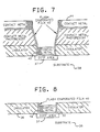
- FIG. 7 illustrates the step of blanket depositing contact metal.
- FIG. 8 illustrates the step of lifting off unwanted metal.
- FIG. 9 illustrates the step of developing the photoresist structure for interconnect metal prior to metal deposition.
- In the preferred embodiment of the invention, a photoresist lift-off process is performed for depositing metal on a semiconductor substrate or ion implanted contacts. Then, a protective film is formed over the etched via holes, prior to the metal deposition step. This prevents the formation of contaminant trapping voids and chemical residues which would otherwise occur at the base and/or sides of the metal subsequently deposited in the etched contact via hole. The protective film, which has a thickness of from 10 to 30 nanometers, remains intact as a permanent part of the structure.
- In prior art methods, alkaline developers attack the contact metal. This is shown in FIGS. 1 through 3 which illustrate the prior art problem. In FIG. 1, the
developer 10 has progressed almost all the way throughphotoresist layer 12, providing a structure for later to be made deposition of interconnect metal but short of contacting the previously depositedcontact metal 14 over the substrate or ion implanteddiffused area 16. In FIG. 2, thedeveloper 10 is shown to have completely removed thephotoresist 12 for subsequently depositing interconnect metal over thecontact 14. Thedeveloper 10 is now in contact withcontact metal 14 at the bottom as well as the sides ofvia hole 18. - In FIG. 3, it is seen that the
developer 10 is actually attacking the physical structure of the previously depositedcontact metal 14 and corroding it thereby leaving avoid 19. The corroded contact metal is shown to have a reducedcross-sectional area 20 which increases the resistance per unit length of the metal contact. This also presents the problem of entrapping some of the alkaline developer and/or otherchemical reaction residues 22 which may present contamination problems, thereby impacting the reliability and life of the product. - The invention is shown in the sequence of steps illustrated in FIGS. 4 through 9. In FIG. 4, a
contact photoresist layer 30 is shown with avia hole 32 made by aphotoresist developer 34 over aninsulator 36. The appropriate portion of the insulator is then wet or dry chemical etched to thesemiconductor substrate 38 as shown in FIG. 5. An ion implant to produce adiffused area 37 in the semiconductor substrate can be done at this time if desired. - Referring to FIG. 6, in accordance with the invention, a flash evaporation step is then performed. From 10 to 30 nanometers of a
protective film 40, such as silicon, is flash evaporated onto theetched contact sidewalls 32. This step protects the sides of the subsequently to be deposited contact metal from attack by alkaline resist developer or other chemical etchants and thereby protects it from corrosion. - Thereafter,
contact metal unwanted contact metal 44 shown in FIG. 7 is lifted off and the desiredremaining contact metal 42 is intact on thesilicon substrate 38 or ion implant diffusedregion 37 in theetched region 32 of theinsulator layer 36. Additional protection can be achieved by depositing an additional protective film over the interface between the metal contact and the via hole to completely seal the device by filling in the gap or void. - As shown in FIG. 9, interconnect
metal photoresist layer 44 is applied, exposed and developed so as to expose thecontact metal 42 which was previously deposited. - For carrying out the process steps for depositing interconnect metal, reference is made to U.S. Patents 4,377,633; 4,076,575; 3,985,597; and 3,873,361. Photolithography and metal deposition procedures can be applied to complete the device and are described in detail in these patents.
- Referring to FIG. 2, by preventing the subsequently applied developer from etching along the interface between the
insulator layer 17 and the lateral sides of themetal contact 14, the cross-sectional dimensions of the contact can be preserved as shown in FIG. 9, thereby maintaining a low electrical contact resistance. This becomes especially important for submicron geometries where this phenomenon of photoresist developer attack of the metal structures produces significantly high contact resistance. An advantage of the present invention is that although contact metal is deposited at an angle to the device wafer surface, primarily because the molten metal source is not at a "line of sight" perpendicular to the wafer surface, no voids or spacing will exist between the contact metal and the sides of the etched insulator. - Although a specific embodiment of the invention has been disclosed, it will be understood by those skilled in the art that the foregoing and other changes in form and details may be made therein without departing ' from the scope of the invention. For example, although silicon has been described as the preferred
protective film 40, other materials such as titanium, germanium, nitride, molybdenum silicide, and tungsten silicide can also be used. It is this class of materials which is preferred because they are resistant to corrosion effects caused by chemicals, and can be deposited with state-of-the-art equipment. However, other protective materials are not precluded from this invention. - Also, although the
semiconductor material 38 is disclosed herein as preferably silicon, other substrate materials such as gallium arsenide and indium phosphide can also be used. - Further, although the
preferred contact metal 42 used in this invention is aluminum, other metals such as molybdenum, tungsten, titanium, and combinations of these materials can be utilized. - The
preferred photoresist 30 utilized with this invention is any positive photoresist. However, other photoresist such as optical materials, electron beam or negative photoresist, wet or dry developable, can also be used.
Claims (11)
- In a semiconductor fabrication process, a method for protecting the sides of a contact metal structure from attack by chemicals used in subsequent process steps, characterized by the step of:depositing a film (40) of protective material, which is resistant to attack by chemicals, on the sides (32) of an etched via hole;depositing a contact metal (42) in the via hole on a semiconductor substrate (38).
- The process of claim 1, including the step of depositing an additional film over the interface between the metal contact and the via holes so as to seal the structure against chemical attack.
- In a metal lift-off process for the deposition of a metal structure for an integrated circuit, a method for protecting the sides of the metal structure from attack by chemicals used in subsequent process steps, comprising the steps of applying a layer of photoresist (30) to an insulator film (36);
- forming a window with sidewalls (32) through the photoresist and insulating film on top of a semiconductor substrate (38); characterized by:
- depositing a layer (40) of protective material, which is resistant to attack by said chemicals, on the surface (32) of said sidewalls of said window;
- depositing contact lift-off metal (42) in the bottom of said window with the sides of the metal structure conforming to said surface of said protective layer covering said sides of said window;
- applying etching chemicals by photoresist removal whereby the sides of said metal structure are not in contact with the chemicals.
- The method of a previous claim, wherein said protective material (40) is selected from the group consisting of silicon, germanium, nitride, molybdenum silicide, and tungsten silicide.
- The method of a previous claim, wherein said substrate (38) is selected from the group consisting of silicon and gallium arsenide; said metal (42) is selected from the group consisting of aluminum, molybdenum, tungsten and titanium; andsaid photoresist (30) is selected from the group consisting of optical photoresist, electron beam photoresist, positive photoresist and negative photoresist, wet or dry developable.
- The method of a previous claim, wherein said subsequently applied chemical is an alkali photoresist developer.
- An electrical contact structure (42, 37) for an integrated circuit, formed through a window (32) in an insulator layer (36) on a silicon substrate (38), characterized by:a thin layer (40) of silicon coating the sidewalls (32) of said window in said insulator layer;a metal contact structure (42) deposited on said silicon (40) in said window, having its edges in contact with the surface of said silicon in said window and in electrical contact with said silicon substrate (38, 37).
Applications Claiming Priority (2)
| Application Number | Priority Date | Filing Date | Title |
|---|---|---|---|
| US06/623,656 US4640738A (en) | 1984-06-22 | 1984-06-22 | Semiconductor contact protection |
| US623656 | 1984-06-22 |
Publications (3)
| Publication Number | Publication Date |
|---|---|
| EP0165513A2 true EP0165513A2 (en) | 1985-12-27 |
| EP0165513A3 EP0165513A3 (en) | 1987-05-13 |
| EP0165513B1 EP0165513B1 (en) | 1991-07-24 |
Family
ID=24498919
Family Applications (1)
| Application Number | Title | Priority Date | Filing Date |
|---|---|---|---|
| EP85106582A Expired - Lifetime EP0165513B1 (en) | 1984-06-22 | 1985-05-29 | Semiconductor contact metal protection |
Country Status (4)
| Country | Link |
|---|---|
| US (1) | US4640738A (en) |
| EP (1) | EP0165513B1 (en) |
| JP (1) | JPS618955A (en) |
| DE (1) | DE3583544D1 (en) |
Cited By (2)
| Publication number | Priority date | Publication date | Assignee | Title |
|---|---|---|---|---|
| EP0266522A2 (en) * | 1986-11-06 | 1988-05-11 | International Business Machines Corporation | Polyimide stud transfer process |
| EP0571108A1 (en) * | 1992-05-06 | 1993-11-24 | STMicroelectronics, Inc. | Semiconductor contact via structure and method |
Families Citing this family (17)
| Publication number | Priority date | Publication date | Assignee | Title |
|---|---|---|---|---|
| US4687541A (en) * | 1986-09-22 | 1987-08-18 | Rockwell International Corporation | Dual deposition single level lift-off process |
| US5238435A (en) * | 1987-06-10 | 1993-08-24 | U.S. Philips Corporation | Liquid crystal display device and method of manufacturing such a display device |
| US5055423A (en) * | 1987-12-28 | 1991-10-08 | Texas Instruments Incorporated | Planarized selective tungsten metallization system |
| US4902379A (en) * | 1988-02-08 | 1990-02-20 | Eastman Kodak Company | UHV compatible lift-off method for patterning nobel metal silicide |
| US4956304A (en) * | 1988-04-07 | 1990-09-11 | Santa Barbara Research Center | Buried junction infrared photodetector process |
| FR2630588A1 (en) * | 1988-04-22 | 1989-10-27 | Philips Nv | METHOD FOR MAKING AN INTERCONNECTION CONFIGURATION ON A SEMICONDUCTOR DEVICE, IN PARTICULAR A HIGH INTEGRATION DENSITY CIRCUIT |
| US4898841A (en) * | 1988-06-16 | 1990-02-06 | Northern Telecom Limited | Method of filling contact holes for semiconductor devices and contact structures made by that method |
| US4981816A (en) * | 1988-10-27 | 1991-01-01 | General Electric Company | MO/TI Contact to silicon |
| US4978637A (en) * | 1989-05-31 | 1990-12-18 | Sgs-Thomson Microelectronics, Inc. | Local interconnect process for integrated circuits |
| JPH03150874A (en) * | 1989-11-07 | 1991-06-27 | Nec Corp | Semiconductor device |
| JPH03156930A (en) * | 1989-11-15 | 1991-07-04 | Sanyo Electric Co Ltd | Semiconductor device |
| JP3086747B2 (en) * | 1992-05-07 | 2000-09-11 | 三菱電機株式会社 | Semiconductor device and manufacturing method thereof |
| US6130482A (en) * | 1995-09-26 | 2000-10-10 | Fujitsu Limited | Semiconductor device and method for fabricating the same |
| US6025256A (en) * | 1997-01-06 | 2000-02-15 | Electro Scientific Industries, Inc. | Laser based method and system for integrated circuit repair or reconfiguration |
| KR100770541B1 (en) * | 2005-12-29 | 2007-10-25 | 동부일렉트로닉스 주식회사 | Semiconductor device and manufacturing method thereof |
| TWI339444B (en) | 2007-05-30 | 2011-03-21 | Au Optronics Corp | Conductor structure, pixel structure, and methods of forming the same |
| DE102013104953B4 (en) * | 2013-05-14 | 2023-03-02 | OSRAM Opto Semiconductors Gesellschaft mit beschränkter Haftung | Optoelectronic component and method for its production |
Citations (1)
| Publication number | Priority date | Publication date | Assignee | Title |
|---|---|---|---|---|
| EP0019781A2 (en) * | 1979-05-29 | 1980-12-10 | International Business Machines Corporation | Method to produce a metal thin film pattern |
Family Cites Families (9)
| Publication number | Priority date | Publication date | Assignee | Title |
|---|---|---|---|---|
| US3985597A (en) * | 1975-05-01 | 1976-10-12 | International Business Machines Corporation | Process for forming passivated metal interconnection system with a planar surface |
| US4076575A (en) * | 1976-06-30 | 1978-02-28 | International Business Machines Corporation | Integrated fabrication method of forming connectors through insulative layers |
| JPS5915174B2 (en) * | 1976-07-26 | 1984-04-07 | 日本電信電話株式会社 | How to make a photomask |
| JPS5475275A (en) * | 1977-11-29 | 1979-06-15 | Fujitsu Ltd | Manufacture of semiconductor device |
| US4410622A (en) * | 1978-12-29 | 1983-10-18 | International Business Machines Corporation | Forming interconnections for multilevel interconnection metallurgy systems |
| US4367119A (en) * | 1980-08-18 | 1983-01-04 | International Business Machines Corporation | Planar multi-level metal process with built-in etch stop |
| US4361599A (en) * | 1981-03-23 | 1982-11-30 | National Semiconductor Corporation | Method of forming plasma etched semiconductor contacts |
| US4377633A (en) * | 1981-08-24 | 1983-03-22 | International Business Machines Corporation | Methods of simultaneous contact and metal lithography patterning |
| US4514751A (en) * | 1982-12-23 | 1985-04-30 | International Business Machines Corporation | Compressively stresses titanium metallurgy for contacting passivated semiconductor devices |
-
1984
- 1984-06-22 US US06/623,656 patent/US4640738A/en not_active Expired - Fee Related
-
1985
- 1985-02-28 JP JP60037731A patent/JPS618955A/en active Granted
- 1985-05-29 EP EP85106582A patent/EP0165513B1/en not_active Expired - Lifetime
- 1985-05-29 DE DE8585106582T patent/DE3583544D1/en not_active Expired - Fee Related
Patent Citations (1)
| Publication number | Priority date | Publication date | Assignee | Title |
|---|---|---|---|---|
| EP0019781A2 (en) * | 1979-05-29 | 1980-12-10 | International Business Machines Corporation | Method to produce a metal thin film pattern |
Non-Patent Citations (4)
| Title |
|---|
| GLOW DISCHARGE PROCESSES, B. CHAPMAN, WILEY and SONS, (1980) PP 232-233 * |
| HANDBOOK OF THIN FILM TECHNOLOGY, EDITED BY I.MAISSEL, R.GLANG, Mc.GRAW-HILL (1970) p 1-92 1-97 * |
| IBM TECHNICAL DISCLOSURE BULLETIN, vol. 24, no. 6, November 1981, pages 2964-2965, New York, US; S.D. EMMANUEL "Low temperature lift-off process" * |
| IBM TECHNICAL DISCLOSURE BULLETIN, vol. 25, no. 4, September 1982, pages 1892-1894, New York, US; A. BROSS et al.: "Lift-off trench process for multilevel metallurgy" * |
Cited By (4)
| Publication number | Priority date | Publication date | Assignee | Title |
|---|---|---|---|---|
| EP0266522A2 (en) * | 1986-11-06 | 1988-05-11 | International Business Machines Corporation | Polyimide stud transfer process |
| EP0266522A3 (en) * | 1986-11-06 | 1988-10-05 | International Business Machines Corporation | Polyimide stud transfer process |
| EP0571108A1 (en) * | 1992-05-06 | 1993-11-24 | STMicroelectronics, Inc. | Semiconductor contact via structure and method |
| US5317192A (en) * | 1992-05-06 | 1994-05-31 | Sgs-Thomson Microelectronics, Inc. | Semiconductor contact via structure having amorphous silicon side walls |
Also Published As
| Publication number | Publication date |
|---|---|
| EP0165513B1 (en) | 1991-07-24 |
| US4640738A (en) | 1987-02-03 |
| DE3583544D1 (en) | 1991-08-29 |
| JPS618955A (en) | 1986-01-16 |
| JPH0312767B2 (en) | 1991-02-21 |
| EP0165513A3 (en) | 1987-05-13 |
Similar Documents
| Publication | Publication Date | Title |
|---|---|---|
| US4640738A (en) | Semiconductor contact protection | |
| US4267012A (en) | Process for patterning metal connections on a semiconductor structure by using a tungsten-titanium etch resistant layer | |
| KR930005949B1 (en) | Process for fabricating semiconductor device | |
| EP0224699B1 (en) | Method of forming fine conductive lines, patterns and connnectors | |
| EP0100735B1 (en) | Lift-off process for fabricating self-aligned contacts | |
| US5369053A (en) | Method for patterning aluminum metallizations | |
| EP0098687A2 (en) | Method of manufacturing a semiconductor device including burying an insulating film | |
| KR940001889B1 (en) | Semiconductor device having a planarized surface | |
| US4029562A (en) | Forming feedthrough connections for multi-level interconnections metallurgy systems | |
| EP0660389A2 (en) | Method of manufacturing semiconductor devices having element separating regions | |
| CA1332323C (en) | Cryogenic process for metal lift off | |
| KR100662945B1 (en) | Improved top layer imaging lithography for semiconductor processing | |
| US6645864B1 (en) | Physical vapor deposition of an amorphous silicon liner to eliminate resist poisoning | |
| US4999317A (en) | Metallization processing | |
| US4847673A (en) | Semiconductor device | |
| US5084415A (en) | Metallization processing | |
| JP2858837B2 (en) | Method for manufacturing semiconductor device | |
| US4679308A (en) | Process for controlling mobile ion contamination in semiconductor devices | |
| JP2892432B2 (en) | Method for manufacturing semiconductor device | |
| US6083823A (en) | Metal deposition process for metal lines over topography | |
| DE102004063264B4 (en) | Method for forming electrical connections in a semiconductor structure | |
| JP2914236B2 (en) | Method for manufacturing semiconductor device | |
| KR100615822B1 (en) | Method for eliminating the particle of semiconductor device | |
| JPS61281523A (en) | Formation of contact | |
| KR100763099B1 (en) | Method of forming a metal-line in semiconductor device |
Legal Events
| Date | Code | Title | Description |
|---|---|---|---|
| PUAI | Public reference made under article 153(3) epc to a published international application that has entered the european phase |
Free format text: ORIGINAL CODE: 0009012 |
|
| AK | Designated contracting states |
Designated state(s): DE FR GB |
|
| 17P | Request for examination filed |
Effective date: 19860424 |
|
| PUAL | Search report despatched |
Free format text: ORIGINAL CODE: 0009013 |
|
| AK | Designated contracting states |
Kind code of ref document: A3 Designated state(s): DE FR GB |
|
| 17Q | First examination report despatched |
Effective date: 19890531 |
|
| GRAA | (expected) grant |
Free format text: ORIGINAL CODE: 0009210 |
|
| AK | Designated contracting states |
Kind code of ref document: B1 Designated state(s): DE FR GB |
|
| REF | Corresponds to: |
Ref document number: 3583544 Country of ref document: DE Date of ref document: 19910829 |
|
| ET | Fr: translation filed | ||
| PLBE | No opposition filed within time limit |
Free format text: ORIGINAL CODE: 0009261 |
|
| STAA | Information on the status of an ep patent application or granted ep patent |
Free format text: STATUS: NO OPPOSITION FILED WITHIN TIME LIMIT |
|
| 26N | No opposition filed | ||
| PGFP | Annual fee paid to national office [announced via postgrant information from national office to epo] |
Ref country code: GB Payment date: 19950413 Year of fee payment: 11 |
|
| PGFP | Annual fee paid to national office [announced via postgrant information from national office to epo] |
Ref country code: FR Payment date: 19950427 Year of fee payment: 11 |
|
| PGFP | Annual fee paid to national office [announced via postgrant information from national office to epo] |
Ref country code: DE Payment date: 19950524 Year of fee payment: 11 |
|
| PG25 | Lapsed in a contracting state [announced via postgrant information from national office to epo] |
Ref country code: GB Effective date: 19960529 |
|
| GBPC | Gb: european patent ceased through non-payment of renewal fee |
Effective date: 19960529 |
|
| PG25 | Lapsed in a contracting state [announced via postgrant information from national office to epo] |
Ref country code: FR Effective date: 19970131 |
|
| PG25 | Lapsed in a contracting state [announced via postgrant information from national office to epo] |
Ref country code: DE Effective date: 19970201 |
|
| REG | Reference to a national code |
Ref country code: FR Ref legal event code: ST |