EP0165863A1 - Method of manufacturing at least one thin film field-effect transistor, and transistor produced by this method - Google Patents
Method of manufacturing at least one thin film field-effect transistor, and transistor produced by this method Download PDFInfo
- Publication number
- EP0165863A1 EP0165863A1 EP85401175A EP85401175A EP0165863A1 EP 0165863 A1 EP0165863 A1 EP 0165863A1 EP 85401175 A EP85401175 A EP 85401175A EP 85401175 A EP85401175 A EP 85401175A EP 0165863 A1 EP0165863 A1 EP 0165863A1
- Authority
- EP
- European Patent Office
- Prior art keywords
- manufacturing
- layer
- electrodes
- resin
- source
- Prior art date
- Legal status (The legal status is an assumption and is not a legal conclusion. Google has not performed a legal analysis and makes no representation as to the accuracy of the status listed.)
- Withdrawn
Links
- 238000000034 method Methods 0.000 title claims abstract description 43
- 238000004519 manufacturing process Methods 0.000 title claims abstract description 30
- 230000005669 field effect Effects 0.000 title claims abstract description 8
- 239000010409 thin film Substances 0.000 title description 6
- 239000000758 substrate Substances 0.000 claims abstract description 15
- 238000005468 ion implantation Methods 0.000 claims abstract description 7
- 239000012212 insulator Substances 0.000 claims description 29
- 239000011347 resin Substances 0.000 claims description 27
- 229920005989 resin Polymers 0.000 claims description 27
- 238000000151 deposition Methods 0.000 claims description 24
- 239000004065 semiconductor Substances 0.000 claims description 20
- 230000008021 deposition Effects 0.000 claims description 16
- 150000002500 ions Chemical class 0.000 claims description 9
- 229910052751 metal Inorganic materials 0.000 claims description 9
- 239000002184 metal Substances 0.000 claims description 9
- 230000015572 biosynthetic process Effects 0.000 claims description 8
- 238000002161 passivation Methods 0.000 claims description 8
- 230000004913 activation Effects 0.000 claims description 6
- 229910021417 amorphous silicon Inorganic materials 0.000 claims description 6
- 239000007789 gas Substances 0.000 claims description 4
- 229910052814 silicon oxide Inorganic materials 0.000 claims description 4
- VYZAMTAEIAYCRO-UHFFFAOYSA-N Chromium Chemical compound [Cr] VYZAMTAEIAYCRO-UHFFFAOYSA-N 0.000 claims description 3
- 229910052581 Si3N4 Inorganic materials 0.000 claims description 3
- VYPSYNLAJGMNEJ-UHFFFAOYSA-N Silicium dioxide Chemical compound O=[Si]=O VYPSYNLAJGMNEJ-UHFFFAOYSA-N 0.000 claims description 3
- 229910052782 aluminium Inorganic materials 0.000 claims description 3
- XAGFODPZIPBFFR-UHFFFAOYSA-N aluminium Chemical compound [Al] XAGFODPZIPBFFR-UHFFFAOYSA-N 0.000 claims description 3
- 239000011651 chromium Substances 0.000 claims description 3
- 230000008030 elimination Effects 0.000 claims description 3
- 238000003379 elimination reaction Methods 0.000 claims description 3
- 230000008020 evaporation Effects 0.000 claims description 3
- 238000001704 evaporation Methods 0.000 claims description 3
- HQVNEWCFYHHQES-UHFFFAOYSA-N silicon nitride Chemical compound N12[Si]34N5[Si]62N3[Si]51N64 HQVNEWCFYHHQES-UHFFFAOYSA-N 0.000 claims description 3
- ZOXJGFHDIHLPTG-UHFFFAOYSA-N Boron Chemical compound [B] ZOXJGFHDIHLPTG-UHFFFAOYSA-N 0.000 claims description 2
- 229910000599 Cr alloy Inorganic materials 0.000 claims description 2
- 229910000990 Ni alloy Inorganic materials 0.000 claims description 2
- OAICVXFJPJFONN-UHFFFAOYSA-N Phosphorus Chemical compound [P] OAICVXFJPJFONN-UHFFFAOYSA-N 0.000 claims description 2
- XUIMIQQOPSSXEZ-UHFFFAOYSA-N Silicon Chemical compound [Si] XUIMIQQOPSSXEZ-UHFFFAOYSA-N 0.000 claims description 2
- 238000000137 annealing Methods 0.000 claims description 2
- 229910052785 arsenic Inorganic materials 0.000 claims description 2
- RQNWIZPPADIBDY-UHFFFAOYSA-N arsenic atom Chemical compound [As] RQNWIZPPADIBDY-UHFFFAOYSA-N 0.000 claims description 2
- 229910052796 boron Inorganic materials 0.000 claims description 2
- 229910052804 chromium Inorganic materials 0.000 claims description 2
- 238000009826 distribution Methods 0.000 claims description 2
- 239000007792 gaseous phase Substances 0.000 claims description 2
- 230000007935 neutral effect Effects 0.000 claims description 2
- 229910052698 phosphorus Inorganic materials 0.000 claims description 2
- 239000011574 phosphorus Substances 0.000 claims description 2
- 238000000206 photolithography Methods 0.000 claims description 2
- 229910052710 silicon Inorganic materials 0.000 claims description 2
- 239000010703 silicon Substances 0.000 claims description 2
- PXHVJJICTQNCMI-UHFFFAOYSA-N Nickel Chemical compound [Ni] PXHVJJICTQNCMI-UHFFFAOYSA-N 0.000 claims 2
- 239000000788 chromium alloy Substances 0.000 claims 1
- 230000000873 masking effect Effects 0.000 abstract description 10
- 239000004973 liquid crystal related substance Substances 0.000 abstract description 3
- 238000004377 microelectronic Methods 0.000 abstract description 2
- 239000007943 implant Substances 0.000 description 5
- 238000009413 insulation Methods 0.000 description 5
- UFHFLCQGNIYNRP-UHFFFAOYSA-N Hydrogen Chemical compound [H][H] UFHFLCQGNIYNRP-UHFFFAOYSA-N 0.000 description 2
- 238000005520 cutting process Methods 0.000 description 2
- 239000011521 glass Substances 0.000 description 2
- 229910052739 hydrogen Inorganic materials 0.000 description 2
- 239000001257 hydrogen Substances 0.000 description 2
- 238000002513 implantation Methods 0.000 description 2
- 239000011159 matrix material Substances 0.000 description 2
- QGZKDVFQNNGYKY-UHFFFAOYSA-N Ammonia Chemical compound N QGZKDVFQNNGYKY-UHFFFAOYSA-N 0.000 description 1
- 229910004298 SiO 2 Inorganic materials 0.000 description 1
- BLRPTPMANUNPDV-UHFFFAOYSA-N Silane Chemical compound [SiH4] BLRPTPMANUNPDV-UHFFFAOYSA-N 0.000 description 1
- 230000003213 activating effect Effects 0.000 description 1
- SVPXDRXYRYOSEX-UHFFFAOYSA-N bentoquatam Chemical compound O.O=[Si]=O.O=[Al]O[Al]=O SVPXDRXYRYOSEX-UHFFFAOYSA-N 0.000 description 1
- 230000005540 biological transmission Effects 0.000 description 1
- 230000003749 cleanliness Effects 0.000 description 1
- 238000000354 decomposition reaction Methods 0.000 description 1
- -1 des ions Chemical class 0.000 description 1
- 238000005984 hydrogenation reaction Methods 0.000 description 1
- 239000012535 impurity Substances 0.000 description 1
- 238000010348 incorporation Methods 0.000 description 1
- 238000002955 isolation Methods 0.000 description 1
- 239000000463 material Substances 0.000 description 1
- 239000000203 mixture Substances 0.000 description 1
- 230000003287 optical effect Effects 0.000 description 1
- 230000035515 penetration Effects 0.000 description 1
- 230000001681 protective effect Effects 0.000 description 1
- 229910000077 silane Inorganic materials 0.000 description 1
- 239000000126 substance Substances 0.000 description 1
Images


Classifications
-
- H—ELECTRICITY
- H01—ELECTRIC ELEMENTS
- H01L—SEMICONDUCTOR DEVICES NOT COVERED BY CLASS H10
- H01L27/00—Devices consisting of a plurality of semiconductor or other solid-state components formed in or on a common substrate
- H01L27/02—Devices consisting of a plurality of semiconductor or other solid-state components formed in or on a common substrate including semiconductor components specially adapted for rectifying, oscillating, amplifying or switching and having at least one potential-jump barrier or surface barrier; including integrated passive circuit elements with at least one potential-jump barrier or surface barrier
- H01L27/12—Devices consisting of a plurality of semiconductor or other solid-state components formed in or on a common substrate including semiconductor components specially adapted for rectifying, oscillating, amplifying or switching and having at least one potential-jump barrier or surface barrier; including integrated passive circuit elements with at least one potential-jump barrier or surface barrier the substrate being other than a semiconductor body, e.g. an insulating body
- H01L27/1214—Devices consisting of a plurality of semiconductor or other solid-state components formed in or on a common substrate including semiconductor components specially adapted for rectifying, oscillating, amplifying or switching and having at least one potential-jump barrier or surface barrier; including integrated passive circuit elements with at least one potential-jump barrier or surface barrier the substrate being other than a semiconductor body, e.g. an insulating body comprising a plurality of TFTs formed on a non-semiconducting substrate, e.g. driving circuits for AMLCDs
- H01L27/1259—Multistep manufacturing methods
- H01L27/1288—Multistep manufacturing methods employing particular masking sequences or specially adapted masks, e.g. half-tone mask
-
- H—ELECTRICITY
- H01—ELECTRIC ELEMENTS
- H01L—SEMICONDUCTOR DEVICES NOT COVERED BY CLASS H10
- H01L27/00—Devices consisting of a plurality of semiconductor or other solid-state components formed in or on a common substrate
- H01L27/02—Devices consisting of a plurality of semiconductor or other solid-state components formed in or on a common substrate including semiconductor components specially adapted for rectifying, oscillating, amplifying or switching and having at least one potential-jump barrier or surface barrier; including integrated passive circuit elements with at least one potential-jump barrier or surface barrier
- H01L27/12—Devices consisting of a plurality of semiconductor or other solid-state components formed in or on a common substrate including semiconductor components specially adapted for rectifying, oscillating, amplifying or switching and having at least one potential-jump barrier or surface barrier; including integrated passive circuit elements with at least one potential-jump barrier or surface barrier the substrate being other than a semiconductor body, e.g. an insulating body
- H01L27/1214—Devices consisting of a plurality of semiconductor or other solid-state components formed in or on a common substrate including semiconductor components specially adapted for rectifying, oscillating, amplifying or switching and having at least one potential-jump barrier or surface barrier; including integrated passive circuit elements with at least one potential-jump barrier or surface barrier the substrate being other than a semiconductor body, e.g. an insulating body comprising a plurality of TFTs formed on a non-semiconducting substrate, e.g. driving circuits for AMLCDs
-
- H—ELECTRICITY
- H01—ELECTRIC ELEMENTS
- H01L—SEMICONDUCTOR DEVICES NOT COVERED BY CLASS H10
- H01L29/00—Semiconductor devices adapted for rectifying, amplifying, oscillating or switching, or capacitors or resistors with at least one potential-jump barrier or surface barrier, e.g. PN junction depletion layer or carrier concentration layer; Details of semiconductor bodies or of electrodes thereof ; Multistep manufacturing processes therefor
- H01L29/66—Types of semiconductor device ; Multistep manufacturing processes therefor
- H01L29/68—Types of semiconductor device ; Multistep manufacturing processes therefor controllable by only the electric current supplied, or only the electric potential applied, to an electrode which does not carry the current to be rectified, amplified or switched
- H01L29/76—Unipolar devices, e.g. field effect transistors
- H01L29/772—Field effect transistors
- H01L29/78—Field effect transistors with field effect produced by an insulated gate
- H01L29/786—Thin film transistors, i.e. transistors with a channel being at least partly a thin film
- H01L29/78651—Silicon transistors
- H01L29/7866—Non-monocrystalline silicon transistors
- H01L29/78663—Amorphous silicon transistors
- H01L29/78666—Amorphous silicon transistors with normal-type structure, e.g. with top gate
-
- Y—GENERAL TAGGING OF NEW TECHNOLOGICAL DEVELOPMENTS; GENERAL TAGGING OF CROSS-SECTIONAL TECHNOLOGIES SPANNING OVER SEVERAL SECTIONS OF THE IPC; TECHNICAL SUBJECTS COVERED BY FORMER USPC CROSS-REFERENCE ART COLLECTIONS [XRACs] AND DIGESTS
- Y10—TECHNICAL SUBJECTS COVERED BY FORMER USPC
- Y10S—TECHNICAL SUBJECTS COVERED BY FORMER USPC CROSS-REFERENCE ART COLLECTIONS [XRACs] AND DIGESTS
- Y10S148/00—Metal treatment
- Y10S148/077—Implantation of silicon on sapphire
-
- Y—GENERAL TAGGING OF NEW TECHNOLOGICAL DEVELOPMENTS; GENERAL TAGGING OF CROSS-SECTIONAL TECHNOLOGIES SPANNING OVER SEVERAL SECTIONS OF THE IPC; TECHNICAL SUBJECTS COVERED BY FORMER USPC CROSS-REFERENCE ART COLLECTIONS [XRACs] AND DIGESTS
- Y10—TECHNICAL SUBJECTS COVERED BY FORMER USPC
- Y10S—TECHNICAL SUBJECTS COVERED BY FORMER USPC CROSS-REFERENCE ART COLLECTIONS [XRACs] AND DIGESTS
- Y10S148/00—Metal treatment
- Y10S148/15—Silicon on sapphire SOS
Definitions
- the present invention relates to a method of manufacturing a field effect transistor, coplanar and self-aligned.
- the method implements three masking levels and uses a thin layer semiconductor. It applies to the field of large-area microelectronics and in particular to the control and addressing of a flat liquid crystal screen or an image sensor.
- the thin film semiconductor best suited to large area devices is hydrogenated amorphous silicon. This is due to the low deposition temperature of the semiconductor which makes it possible to use transparent and economical substrates such as glass and also to the uniformity of the layer deposited, even on large surfaces.
- the use of this material imposes four main constraints which it is necessary to respect in order to obtain devices having optimal performance.
- the deposits of the semiconductor and gate insulator layers must be carried out in stride and in the same enclosure in order to preserve, a good quality of the semiconductor-insulator interface.
- a - Si: H hydrogenated amorphous silicon
- the need to have good source and drain contacts requires the use of a layer of hydrogenated amorphous silicon which is strongly doped in contact with the source and drain electrodes.
- Good quality source and drain contacts can be obtained by means of an intermediate layer of a - Si: H doped during deposition by addition of an additional gas containing a doping element or by means of ion implantation.
- the distances between the channel and the source contacts on the one hand and the drain contacts on the other hand must be minimal.
- the source and drain contacts as well as the grid must be precisely defined (self-alignment of the electrodes) in order to reduce the stray capacitances occurring through the grid insulator.
- the source and drain contacts as well as the grid must be located on the same side of the semiconductor layer in order to suppress the access resistance through the thickness of said layer. In the majority of thin film transistors currently manufactured, the gate and the source and drain contacts partially overlap and are placed on either side of the a - Si: H layer.
- the fourth production constraint consists of the number of masking levels.
- Four masking levels are generally used for the manufacture of thin film transistors in a - Si: H. Three levels are sufficient for the self-aligned process. To increase the manufacturing yield and decrease the cost, it is necessary to limit the number of masking levels to the strict minimum.
- the subject of the invention is also a thin-film field effect transistor, of the coplanar type and with self-aligned electrodes produced on an insulating substrate, characterized in that it is obtained by the manufacturing process described above.
- TFT thin film transistors
- the process according to the invention is a collective manufacturing process.
- the drawings will only show the manufacture of a transistor.
- Figure 1 is illustrative of the first step of the manufacturing process according to the invention.
- This step consists in depositing on a transparent substrate 1, a layer 2 of hydrogenated amorphous silicon a - Si: H, then a layer of insulator 3. If the substrate is glass, the deposition methods must be carried out at a temperature which does not alter its properties.
- a deposition temperature of the order of 200 to 300 ° C. can be obtained by a method of deposition in the gaseous phase by luminescent discharge.
- the hydrogenation results from an incorporation during the deposition according to a known method.
- the insulating layer 3 is deposited in the wake of the layer 2 by the same plasma gas decomposition process, the nature of which depends on the insulating species which it is desired to obtain. For example, if the insulator 3 is silicon nitride Si 3 N 4, a mixture of silane Si H 4 and ammonia gas NH 3 will be decomposed. Insulators such as silicon oxide SiO 2 and silicon oxynitride SiON may also be suitable.
- the deposition temperature of layer 3 must not be higher than the deposition temperature of the layer of a - Si: H so that the hydrogen does not leave this layer.
- the thicknesses of the deposits are of the order of 0.2 to 0.5 ⁇ m for the layer 2 of a - Si: H and from 0.1 to 0.2, ⁇ m for the layer of insulator.
- Figures 2 and 3 are illustrative of the second step of the process.
- Figure 2 is a front view corresponding to Figure 1 and Figure 3 is a top view.
- This second step consists of the first level of masking used to delimit the mesas on which the transistors will be produced.
- the procedure is known: protection by a layer of resin 4 of the parts to be preserved (one mesa by future transistor) and attack on the part to be eliminated by chemical or dry means (plasma).
- the superposition of the three layers is thus obtained on the substrate 1: semiconductor 2 - insulator 3 - resin 4.
- the dimensions of the mesas will depend on the intensity of the current which each transistor will have to support. A possible order of size, for the type of use proposed, is approximately 30 ⁇ m by 100 ⁇ m.
- Figures 4 and 5 are illustrative of the third step of the method which consists in depositing a passivation insulator on the flanks of the mesa in order to avoid short-circuits between source or drain on the one hand and gate on the other hand.
- a layer 5 of insulation is deposited by one of the methods of deposition mentioned.
- the insulator may be silicon oxide Si O 2 ; silicon nitride Si 3 N 4 or another insulator.
- the passivation insulation layer can be 0.5 ⁇ m thick.
- the fourth step consists in depositing the grid metal, generally aluminum, and in carrying out a conventional photolithographic cutting of the metal grid which constitutes the second level of masking.
- a metal layer 6 with a thickness of about 0.2 microns deposited by evaporation.
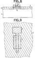
- a mask 7 of resin deposited on the metal layer 6. This mask will delimit the gate electrode 61 of the transistor. This will, for example, have a T shape whose width L (of the order of 2 to 10 ⁇ m) of the vertical part will determine the length of the transistor channel and whose horizontal strikethrough will serve as an electrical contact.
- Figures 8 and 9 which also represent front and top views, are illustrative of the device obtained at the end of the fourth step of the method where the gate electrode 61 is covered with the mask 7 which served to delimit it.
- the fifth step consists in attacking, chemically or dry, the gate insulator not located directly under the gate electrode 61 so as to expose the lateral areas of a -Si: H on which the source contacts will be formed. and drain.
- this step all or part of the passivation insulator 5 not protected by the assembly formed by the arille electrode 61 and the resin 7 can be eliminated, the isolation sought on the flanks of the mesa where the gate electrode not affected by this attack. Or made of the difference in thickness between the layers of insulation 3 and 5, the second being approximately 5 times thicker than the first, it is possible to keep a determined thickness of passivation insulation.
- the device obtained is in the form shown in Figures 10 and 11 which are respectively a front view and a top view.
- the sixth step of the process consists in obtaining ohmic source and drain contacts on the discovered semiconductor layer.
- the technique of ion implantation at ambient temperature is used.
- Figure 12 illustrates this step of the process.
- the implanted ions are for example: phosphorus or arsenic to have n-type contacts, boron to have p-type contacts.
- the self-alignment is obtained by the gate electrode itself covered with resin. This resin layer provides additional protection to prevent the penetration of implants into the gate insulator.
- the doses of implanted ions are of the order of some 10 16 / cm 2 for an energy varying from 50 to 250 keV depending on the thickness of the semiconductor layer and in the case of an n contact. It is advantageous to implant at different energy levels in order to optimize the distribution of the implanted ions as a function of the performances required from the transistors.
- the seventh step of the process consists of removing the protective resin from the gate electrode and then activating the implants.
- the resin is removed chemically or dry.
- the activation of the implants is carried out by annealing under a neutral gas flow at a temperature of the order of 200 to 300 ° C., that is to say compatible with the non-exodiffusion of the hydrogen from the layer. of a - If: H.
- the advantage of this method is to avoid the formation of an access resistance of the transistor channel.
- figure 13 represents the device obtained after the elimination of the resin and activation of the implants.
- the seventh step is to remove the resin from the grid. A plasma attack will be necessary because the resin will have been annealed.
- the eighth and last step is constituted by the development of the metal source and drain contacts on the doped semiconductor. This is achieved by a third level of masking and by the so-called lift-off technique.
- the metal contacts will generally be made of aluminum and deposited by evaporation. They can also be produced in chromium or in an alloy of nickel and chromium. nans such an embodiment, the length of the channel is defined by the aril and the width by the mesa so that the positioning of the source and the drain is not very critical compared to the grid and the mesa.
- the sensitive point is to avoid the short circuit that could occur between the gate electrode and the source and draina electrodes.
- the manufacturing method according to the invention leads to a structure which has a channel whose length is determined by the grid and whose width is determined by the mesa.
- the metal layer 9 can, in addition to the formation of the source and drain electrodes of each transistor, also serve to form conductive strips of access to either source electrodes, ie at the drain electrodes.
- This screen can be used in transmission since the substrate is transparent and the passivation insulator, which largely covers it, is also used because of its optical properties and its low thickness.
Abstract
L'invention concerne un procédé de fabrication de transistors à effet de champ de type coplanaire et auto-aligné, obtenus en couche mince sur un substrat isolant (1). Le procédé permet, grâce à des techniques d'auto-alignement des électrodes (61, 91, 92) et d'implantation ionique, de n'utiliser que trois niveaux de masquage. L'invention s'applique au domaine de la microélectronique en grande surface et en particulier à la commande et à l'adressage d'un écran plat à cristal liquide ou d'un capteur d'images.The invention relates to a method for manufacturing self-aligned coplanar type field effect transistors obtained on a thin layer on an insulating substrate (1). The method makes it possible, using self-alignment techniques for the electrodes (61, 91, 92) and ion implantation, to use only three masking levels. The invention applies to the field of large-area microelectronics and in particular to the control and addressing of a flat liquid crystal screen or an image sensor.
Description
La présente invention concerne un procédé de fabrication d'un transistor à effet de champ, coplanaire et auto-aligné. Le procédé met en oeuvre trois niveaux de masquage et utilise un semiconducteur en couche mince. Il s'applique au domaine de la microélectronique en grande surface et en particulier à la commande et à l'adressaqe d'un écran plat à cristal liquide ou d'un capteur d'images.The present invention relates to a method of manufacturing a field effect transistor, coplanar and self-aligned. The method implements three masking levels and uses a thin layer semiconductor. It applies to the field of large-area microelectronics and in particular to the control and addressing of a flat liquid crystal screen or an image sensor.
Actuellement, le semiconducteur en couche mince le mieux adapté aux dispositifs en grande surface est le silicium amorphe hydrogéné. Ceci est d0 à la faible température 'de dépôt du semiconducteur qui rend possible l'utilisation de substrats transparents et économiques tels que le verre et également à l'homogénéité de la couche , déposée, même sur de grandes surfaces.. Cependant, l'utilisation de ce matériau impose quatre contraintes principales qu'il est nécessaire de respecter afin d'obtenir des dispositifs ayant des performances optimales.Currently, the thin film semiconductor best suited to large area devices is hydrogenated amorphous silicon. This is due to the low deposition temperature of the semiconductor which makes it possible to use transparent and economical substrates such as glass and also to the uniformity of the layer deposited, even on large surfaces. However, the use of this material imposes four main constraints which it is necessary to respect in order to obtain devices having optimal performance.
Première contrainte, les dépôts des couches de semiconducteur et d'isolant de grille doivent être réalisés dans la foulée et dans la même enceinte afin de préserver, une bonne qualité de l'interface semiconducteur- isolant. Dans le cas du silicium amorphe hydrogéné (a - Si : H) ceci est généralement respecté car les dispositifs utilisés pour déposer le a - Si : H permettent également le dépôt de l'isolant de grille sans altérer la propreté du premier dépôt.First constraint, the deposits of the semiconductor and gate insulator layers must be carried out in stride and in the same enclosure in order to preserve, a good quality of the semiconductor-insulator interface. In the case of hydrogenated amorphous silicon (a - Si: H) this is generally respected because the devices used to deposit the a - Si: H also allow the deposition of the gate insulator without altering the cleanliness of the first deposit.
Deuxième contrainte de fabrication, la nécessité de disposer de bons contacts source et drain impose l'utilisation d'une couche de silicium amorphe hydrogéné qui soit fortement dopée en contact avec les électrodes de source et de drain. Des contacts source et drain de bonne qualité peuvent être obtenus au moyen d'une couche intermédiaire de a - Si : H dopé durant le dépôt par addition d'un gaz supplémentaire contenant un élément dopant ou au moyen de l'implantation ionique.Second manufacturing constraint, the need to have good source and drain contacts requires the use of a layer of hydrogenated amorphous silicon which is strongly doped in contact with the source and drain electrodes. Good quality source and drain contacts can be obtained by means of an intermediate layer of a - Si: H doped during deposition by addition of an additional gas containing a doping element or by means of ion implantation.
Troisième contrainte de fabrication, en raison de la faible conductivité du silicium amorphe hydrogéné, les distances entre le canal et les contacts source d'une part et drain d'autre part doivent être minimales. Les contacts de source et de drain ainsi que la grille doivent être définis de manière précise (auto-alignement des électrodes) afin de réduire les capacités parasites se présentant à travers l'isolant de grille. Les contacts de source et de drain ainsi que la grille doivent être situés du même côté de la couche de semiconducteur afin de supprimer la résistance d'accès à travers l'épaisseur de ladite couche. Dans la majorité des transistors en couche mince fabriqués actuellement, la grille et les contacts de source et de drain se recouvrent partiellement et sont placés de part et d'autre de la couche de a - Si : H. Il est apparu récemment une méthode d'auto-alignement permettant la réalisation de transistors en couche mince en configuration dite "staggered" dans la terminologie anglo-saxonne (c'est-à-dire présentant la succession : substrat-grille-isolant-semiconducteur-contacts de drain et de source). Cette méthode a fait l'objet d'un article intitulé "A self-alignment processed a - Si TFT matrix circuit for LCD panels" par ASAMA et al dans la revue SID 83 Digest, pages 144 et 145. La découpe des contacts source et drain dans la couche de a - Si : H dopée n est réalisée par une insolation depuis le substrat ce qui permet à la grille de servir de masque. Cette technique n'est applicable qu'à ce type de structure dans laquelle grille et contacts sont de part et d'autre de la couche de a - Si : H qui doit être suffisamment mince pour être transparente.Third manufacturing constraint, due to the low conductivity of the hydrogenated amorphous silicon, the distances between the channel and the source contacts on the one hand and the drain contacts on the other hand must be minimal. The source and drain contacts as well as the grid must be precisely defined (self-alignment of the electrodes) in order to reduce the stray capacitances occurring through the grid insulator. The source and drain contacts as well as the grid must be located on the same side of the semiconductor layer in order to suppress the access resistance through the thickness of said layer. In the majority of thin film transistors currently manufactured, the gate and the source and drain contacts partially overlap and are placed on either side of the a - Si: H layer. A method d recently appeared 'self-alignment allowing the realization of thin layer transistors in configuration called "staggered" in English terminology (that is to say having the succession: substrate-grid-insulator-semiconductor-drain and source contacts ). This method was the subject of an article entitled "A self-alignment processed a - Si TFT matrix circuit for LCD panels" by ASAMA et al in the review SID 83 Digest, pages 144 and 145. Cutting the source contacts and drain in the layer of a - Si: H doped n is produced by exposure from the substrate which allows the grid to serve as a mask. This technique is only applicable to this type of structure in which grid and contacts are on either side of the layer of a - Si: H which must be thin enough to be transparent.
La quatrième contrainte de réalisation est constituée par le nombre de niveaux de masquage. Quatre niveaux de masquage sont généralement utilisés pour la fabrication des transistors en couche mince en a - Si : H. Trois niveaux suffisent au procédé auto-aligné. Pour augmenter le rendement de fabrication et en diminuer le coût, il est nécessaire de limiter le nombre des niveaux de masquage au strict minimum.The fourth production constraint consists of the number of masking levels. Four masking levels are generally used for the manufacture of thin film transistors in a - Si: H. Three levels are sufficient for the self-aligned process. To increase the manufacturing yield and decrease the cost, it is necessary to limit the number of masking levels to the strict minimum.
A ce jour, aucun des procédés connus ne permet de satisfaire les quatre contraintes énumérées ci-dessus. Le procédé de fabrication selon l'invention satisfait ces contraintes par des techniques d'auto-alignement et d'implantation ionique. Il permet de réduire à trois le nombre des niveaux de masquage.To date, none of the known methods makes it possible to satisfy the four constraints listed above. The manufacturing process according to the invention satisfies these constraints by self-alignment and ion implantation techniques. It allows the number of masking levels to be reduced to three.
L'invention a donc pour objet un procédé de fabrication d'au moins un transistor à effet de champ, en couche mince, de type coplanaire et à auto-alignement des électrodes, caractérisé en ce que le procède comprend les huit étapes suivantes :
- - première étape : dépôts successifs sur un substrat d'une couche semiconductrice et d'une couche d'isolant de grille,
- - deuxième étape : formation de mésas par un premier jeu de masques de résine et par attaque des couches d'isolant de grille et semiconductrice jusqu'au niveau du substrat, chacune des mésas étant destinée à la formation d'un transistor,
- - troisième étape : dépôt d'une couche d'isolant de passivation et mise à nu de l'isolant de grille par retrait de la résine,
- - quatrième étape : dépôt des électrodes de grille des transistors par un deuxième jeu de masques de résine et photolithographie,
- - cinquième étape : attaque de la couche d'isolant de grille non recouverte par les électrodes de grille jusqu'à mise à nu de la couche semiconductrice,
- - sixième étape : obtention de contacts ohmiques de source et de drain par implantation ionique,
- - septième étape : élimination de la résine de protection de grille suivie d'une activation des ions implantés à l'étape précédente,
- - huitième étape : dépôt des électrodes de source et de drain par un troisième jeu de masques de résine et retrait de la résine.
- first step: successive depositions on a substrate of a semiconductor layer and a gate insulator layer,
- second step: formation of mesas by a first set of resin masks and by attacking the layers of gate and semiconductor insulation up to the level of the substrate, each of the mesas being intended for the formation of a transistor,
- - third step: depositing a layer of passivation insulator and exposing the gate insulator by removing the resin,
- - fourth step: deposition of the gate electrodes of the transistors by a second set of resin masks and photolithography,
- - fifth step: attack of the gate insulator layer not covered by the gate electrodes until the semiconductor layer is exposed,
- - sixth step: obtaining ohmic source and drain contacts by ion implantation,
- - seventh step: elimination of the gate protection resin followed by activation of the ions implanted in the previous step,
- - eighth step: deposition of the source and drain electrodes by a third set of resin masks and removal of the resin.
L'invention a aussi pour objet un transistor à effet de champ en couche mince, de type coplanaire et à électrodes auto-alignées réalisé sur un substrat isolant, caractérisé en ce qu'il est obtenu par le procédé de fabrication exposé ci-dessus.The subject of the invention is also a thin-film field effect transistor, of the coplanar type and with self-aligned electrodes produced on an insulating substrate, characterized in that it is obtained by the manufacturing process described above.
L'invention sera mieux comprise et d'autres avantages apparaîtront à la lecture de la description qui va suivre et d'après les figures annexées parmi lesquelles :
- - la figure 1 illustre la première étape du procédé selon l'invention,
- - les figures 2 et 3 illustrent la seconde étape du procédé,
- - les figures 4 et 5 illustrent la troisième étape du procédé,
- - les figures 6 à 9 illustrent la quatrième étape du procédé,
- - les figures 10 et 11 illustrent la cinquième étape du procédé,
- - la figure 12 illustre la sixième étape du procédé,
- - la figure 13 illustre la septième étape du procédé,
- - les figures 14 à 16 illustrent la huitième étape du procédé.
- FIG. 1 illustrates the first step of the method according to the invention,
- FIGS. 2 and 3 illustrate the second step of the process,
- FIGS. 4 and 5 illustrate the third step of the method,
- FIGS. 6 to 9 illustrate the fourth step of the method,
- FIGS. 10 and 11 illustrate the fifth step of the method,
- FIG. 12 illustrates the sixth step of the method,
- FIG. 13 illustrates the seventh step of the method,
- - Figures 14 to 16 illustrate the eighth step of the process.
La description va porter, à titre d'exemple, sur un procédé de fabrication de transistors en couche mince (TFT) réalisés sur a - Si : H sur un substrat faisant partie d'un écran de visualisation à cristal liquide. Ces transistors sont alors destinés à l'adressage et à la commande intégrée de dispositifs en grande surface. Le procédé selon l'invention est également applicable à d'autres semiconducteurs amorphes ou polycristallins déposés en couche mince.The description will relate, by way of example, to a process for manufacturing thin film transistors (TFT) produced on a - Si: H on a substrate forming part of a liquid crystal display screen. These transistors are then intended for addressing and integrated control of devices in large areas. The method according to the invention is also applicable to other amorphous or polycrystalline semiconductors deposited in a thin layer.
Le procédé selon l'invention est un procédé collectif de fabrication. Par souci de simplification, les dessins ne montreront que la fabrication d'un transistor.The process according to the invention is a collective manufacturing process. For the sake of simplification, the drawings will only show the manufacture of a transistor.
La figure 1 est illustrative de la première étape du procédé de fabrication selon l'invention. Cette étape consiste à déposer sur un substrat transparent 1, une couche 2 de silicium amorphe hydrogéné a - Si : H, puis une couche d'isolant 3. Si le substrat est en verre, les méthodes de dépôt doivent être réalisées à une température qui n'altère pas ses propriétés. Pour le semiconducteur, une température de dépôt de l'ordre de 200 à 3000 C peut être obtenue par une méthode de dépôt en phase gazeuse par décharge luminescente. L'hydrogénation résulte d'une incorporation pendant le dépôt selon une méthode connue. La couche d'isolant 3 est déposée dans la foulée de la couche 2 par le même procédé de décomposition plasma de gaz dont la nature dépend de l'espèce isolante que l'on veut obtenir. Par exemple, si l'isolant 3 est du nitrure de silicium Si3N4 on procédera à la décomposition d'un mélange de silane Si H4 et de gaz ammoniac NH3. Des isolants tels que l'oxyde de silicium SiO2 et l'oxynitrure de silicium SiON peuvent également convenir. La température de dépôt de la couche 3 ne doit pas être supérieure à la température de dépôt de la couche de a - Si : H afin que l'hydrogène ne quitte pas cette couche. Typiquement, les épaisseurs des dépôts sont de l'ordre de 0,2 à 0,5 µm pour la couche 2 de a - Si : H et de 0,1 à 0,2 ,um pour la couche d'isolant.Figure 1 is illustrative of the first step of the manufacturing process according to the invention. This step consists in depositing on a
Les figures 2 et 3 sont illustratives de la seconde étape du procédé. La figure 2 est une vue de face correspondant à le figure 1 et la figure 3 est une vue de dessus. Cette seconde étape est constituée par le premier niveau de masquage servant à délimiter les mésas sur lesquelles seront élaborés les transistors. La manière de procéder est connue : protection par une couche 4 de résine des parties à conserver (une mésa par futur transistor) et attaque de la partie à éliminer par voie chimique ou sèche (plasma). On obtient ainsi sur le substrat 1 la superposition des trois couches : semiconducteur 2 - isolant 3 - résine 4. Les dimensions des mésas dépendront de l'intensité du courant que devra supporter chaque transistor. Un ordre de qrandeur possible, pour le type d'utilisation proposé, est d'environ 30 µm sur 100 µm.Figures 2 and 3 are illustrative of the second step of the process. Figure 2 is a front view corresponding to Figure 1 and Figure 3 is a top view. This second step consists of the first level of masking used to delimit the mesas on which the transistors will be produced. The procedure is known: protection by a layer of
Les figures 4 et 5 sont illustratives de la troisième étape du procédé qui consiste à déposer un isolant de passivation des flancs de la mésa afin d'éviter les court-circuits entre source ou drain d'une part et grille d'autre part. Comme représenté à la figure 4, une couche 5 d'isolant est déposée par l'une des méthodes de dépôt citées. L'isolant peut être de l'oxyde de silicium Si O2; du nitruré de silicium Si3 N4 ou un autre isolant. La couche d'isolant de passivation peut avoir 0,5 µm d'épaisseur. Par la méthode dite de lift-off, les éléments de résine 4 restant de la seconde étape sont éliminés ce qui a pour objet de faire réapparaître l'isolant de grille déposé au cours de la première étape, comme l'indique la figure 5.Figures 4 and 5 are illustrative of the third step of the method which consists in depositing a passivation insulator on the flanks of the mesa in order to avoid short-circuits between source or drain on the one hand and gate on the other hand. As shown in FIG. 4, a
La quatrième étape consiste à déposer le métal de grille, en général de l'aluminium, et à procéder à une découpe photolithographique classique de la grille métallique ce qui constitue le second niveau de masquage. Aux figures 6 et 7, qui représentent des vues de face et de dessus, on distingue la couche métallique 6 d'une épaisseur d'environ 0,2 µm déposée par évaporation. On distingue également un masque 7 de résine déposé sur la couche métallique 6. Ce masque va délimiter l'électrode de grille 61 du transistor. Celle-ci aura par exemple une forme en T dont la largeur L (de l'ordre de 2 à 10 µm) de la partie verticale déterminera la longueur du canal du transistor et dont la barré horizontale servira de prise de contact électrique. Les figures 8 et 9 qui représentent également des vues de face et de dessus, sont illustratives du dispositif obtenu à l'issue de la quatrième étape du procédé où l'électrode de grille 61 est recouverte du masque 7 qui a servi à la délimiter.The fourth step consists in depositing the grid metal, generally aluminum, and in carrying out a conventional photolithographic cutting of the metal grid which constitutes the second level of masking. In Figures 6 and 7, which show front and top views, there is a
La cinquième étape consiste è attaquer, par voie chimique ou sèche, l'isolant de grille non situé directement sous l'électrode de grille 61 de façon à mettre à découvert les plages latérales de a -Si : H sur lesquelles seront formés les contacts source et drain. Dans cette étape, tout ou partie de l'isolant de passivation 5 non protégé par l'ensemble formé par l'électrode de arille 61 et la résine 7 peut être éliminé, l'isolement recherché sur les flancs de la mésa où déborde l'électrode de grille n'étant pas affecté par cette attaque. Ou fait de la différence d'épaisseur entre les couches d'isolant 3 et 5, la seconde étant environ 5 fois plus épaisse que la première, il est possible de garder une épaisseur déterminée d'isolant de passivation. A l'issue de cette étape, le dispositif obtenu se présente sous la forme représentée à aux figures 10 et 11 qui sont respectivement une vue de face et une vue de dessus.The fifth step consists in attacking, chemically or dry, the gate insulator not located directly under the
La sixième étape du procédé consiste en l'obtention de contacts ohmiques de source et de drain sur la couche de semiconducteur découverte. On emploie la technique d'implantation ionique à température ambiante. La figure 12 illustre cette étape du procédé. Les ions implantés sont par exemple : le phosphore ou l'arsenic pour disposer de contacts de type n, le bore pour disposer de contacts de type p. L'auto-alignement est obtenu par l'électrode de grille elle-méme recouverte de résine. Cette couche de résine constitue une protection supplémentaire pour éviter la pénétration d'implants dans l'isolant de grille. Typiquement, les doses d'ions implantés sont de l'ordre de quelques 1016/cm2 pour une énergie variant de 50 à 250 keV selon l'épaisseur de la couche de semiconducteur et dans le cas d'un contact n. Il est intéressant de procéder à une implantation à différents niveaux d'énergie afin d'optimiser la répartition des ions implantés en fonction des performances demandées aux transistors.The sixth step of the process consists in obtaining ohmic source and drain contacts on the discovered semiconductor layer. The technique of ion implantation at ambient temperature is used. Figure 12 illustrates this step of the process. The implanted ions are for example: phosphorus or arsenic to have n-type contacts, boron to have p-type contacts. The self-alignment is obtained by the gate electrode itself covered with resin. This resin layer provides additional protection to prevent the penetration of implants into the gate insulator. Typically, the doses of implanted ions are of the order of some 10 16 / cm 2 for an energy varying from 50 to 250 keV depending on the thickness of the semiconductor layer and in the case of an n contact. It is advantageous to implant at different energy levels in order to optimize the distribution of the implanted ions as a function of the performances required from the transistors.
La septième étape du procédé consiste à éliminer la résine de protection de l'électrode de grille puis à faire une activation des implants. La résine est éliminée par voie chimique ou sèche. L'activation des implants est réalisée par un recuit sous un flux de gaz neutre à une température de l'ordre de 200 à 3000 C, c'est-à-dire compatible avec la non-exodiffusion de l'hydrogène de la couche de a - Si : H. L'avantage de cette méthode est d'éviter la formation d'une résistance d'accès du canal du transistor. Cette étape est illustrée par la figure 13 qui représente le dispositif obtenu après l'élimination de la résine et activation des implants.The seventh step of the process consists of removing the protective resin from the gate electrode and then activating the implants. The resin is removed chemically or dry. The activation of the implants is carried out by annealing under a neutral gas flow at a temperature of the order of 200 to 300 ° C., that is to say compatible with the non-exodiffusion of the hydrogen from the layer. of a - If: H. The advantage of this method is to avoid the formation of an access resistance of the transistor channel. This step is illustrated by figure 13 which represents the device obtained after the elimination of the resin and activation of the implants.
Il est aussi possible de réaliser la sixième étape à une température comprise entre 200 et 300°C et ainsi d'activer les impuretés dès leur implantation. Dans ce cas, la septième étape consiste à retirer la résine de la grille. Une attaque plasma sera nécessaire car la résine aura été recuite.It is also possible to perform the sixth step at a temperature between 200 and 300 ° C and thus activate the impurities from their implantation. In this case, the seventh step is to remove the resin from the grid. A plasma attack will be necessary because the resin will have been annealed.
La huitième et dernière étape est constituée par l'élaboration des contacts métalliques source et drain sur le semiconducteur dopé. Ceci est obtenu par un troisième niveau de masquage et par la technique dite de lift-off. Les contacts métalliques seront en général en aluminium et déposés par évaporation. On peut encore les réaliser en chrome ou en un alliage de nickel et de chrome. nans un tel procédé de réalisation, la longueur du canal est définie par la arille et la largeur par la mésa si bien que le positionnement de la source et du drain n'est pas très critique par rapport à la grille et la mésa. Le point sensible est d'éviter le court-circuit qui pourrait se produire entre l'électrode de grille et les électrodes de source et de draina A cette fin, il est préférable de réserver une marge de sécurité déterminée entre ces contacts, typiquement de l'ordre de 5 à 10 µm. Cette distance est compatible avec une extension du procédé pour la réalisation de grandes surfaces, par exemple 20 cm sur 20 cm. Les figures 14, 15 et 16 sont illustratives de cette dernière étape du procédé. Par des techniques de masquage connues, on dépose des éléments de résine 8 sur chaque futur transistor. Chaque élément de résine 8 recouvre toutes les parties à ne pas métalliser, notamment : l'électrode de grille 61, la couche d'isolant de grille 3 sous-jacente et les parties de semiconducteur dopé à ne pas métalliser. La couche métallique 9 a une épaisseur sensiblement égale à 0,2 µm. Les figures 15 et 16 présentent une vue de face et une vue de dessus de la structure finale obtenue. L'opération de lift-off de la résine permet de donner au transistor sa structure finale en délimitant les électrodes de source 91 et de drain 92.The eighth and last step is constituted by the development of the metal source and drain contacts on the doped semiconductor. This is achieved by a third level of masking and by the so-called lift-off technique. The metal contacts will generally be made of aluminum and deposited by evaporation. They can also be produced in chromium or in an alloy of nickel and chromium. nans such an embodiment, the length of the channel is defined by the aril and the width by the mesa so that the positioning of the source and the drain is not very critical compared to the grid and the mesa. The sensitive point is to avoid the short circuit that could occur between the gate electrode and the source and draina electrodes. To this end, it is preferable to reserve a determined safety margin between these contacts, typically of the '' from 5 to 10 µm. This distance is compatible with an extension of the process for the production of large areas, for example 20 cm by 20 cm. Figures 14, 15 and 16 are illustrative of this last step of the process. By known masking techniques, resin elements 8 are deposited on each future transistor. Each resin element 8 covers all the parts not to be metallized, in particular: the
On peut remarquer que le procédé de fabrication selon l'invention conduit à une structure qui possède un canal dont la longueur est déterminée par la grille et dont la larqeur est déterminée par la mésa.It can be noted that the manufacturing method according to the invention leads to a structure which has a channel whose length is determined by the grid and whose width is determined by the mesa.
Dans le cadre de la réalisation d'un écran de visualisation à accès matriciel, la couche métallique 9 peut, en plus de la formation des électrodes de source et de drain de chaque transistor, servir également à former des bandes conductrices d'accès soit aux électrodes sources, soit aux électrodes drain. Cet écran peut être utilisé en transmission puisque le substrat est transparent et que l'isolant de passivation, qui le recouvre en grande partie, l'est aussi de par ses propriétés optiques et sa faible épaisseur.In the context of the production of a display screen with matrix access, the
Claims (13)
Applications Claiming Priority (2)
| Application Number | Priority Date | Filing Date | Title |
|---|---|---|---|
| FR8409875 | 1984-06-22 | ||
| FR8409875A FR2566583B1 (en) | 1984-06-22 | 1984-06-22 | METHOD FOR MANUFACTURING AT LEAST ONE THIN FILM FIELD-EFFECT TRANSISTOR, AND TRANSISTOR OBTAINED BY THIS METHOD |
Publications (1)
| Publication Number | Publication Date |
|---|---|
| EP0165863A1 true EP0165863A1 (en) | 1985-12-27 |
Family
ID=9305346
Family Applications (1)
| Application Number | Title | Priority Date | Filing Date |
|---|---|---|---|
| EP85401175A Withdrawn EP0165863A1 (en) | 1984-06-22 | 1985-06-13 | Method of manufacturing at least one thin film field-effect transistor, and transistor produced by this method |
Country Status (4)
| Country | Link |
|---|---|
| US (1) | US4704784A (en) |
| EP (1) | EP0165863A1 (en) |
| JP (1) | JPS6113670A (en) |
| FR (1) | FR2566583B1 (en) |
Cited By (1)
| Publication number | Priority date | Publication date | Assignee | Title |
|---|---|---|---|---|
| EP0457596A2 (en) * | 1990-05-17 | 1991-11-21 | Sharp Kabushiki Kaisha | Process for fabricating a thin film transistor |
Families Citing this family (9)
| Publication number | Priority date | Publication date | Assignee | Title |
|---|---|---|---|---|
| FR2579806B1 (en) * | 1985-03-26 | 1987-05-07 | Morin Francois | METHOD FOR MANUFACTURING A LIQUID CRYSTAL AND DIODE ARRAY DISPLAY SCREEN |
| US4803173A (en) * | 1987-06-29 | 1989-02-07 | North American Philips Corporation, Signetics Division | Method of fabrication of semiconductor device having a planar configuration |
| US4918504A (en) * | 1987-07-31 | 1990-04-17 | Nippon Telegraph And Telephone Corporation | Active matrix cell |
| JP3122995B2 (en) * | 1989-02-27 | 2001-01-09 | 株式会社日立製作所 | Liquid crystal display |
| US5403762A (en) | 1993-06-30 | 1995-04-04 | Semiconductor Energy Laboratory Co., Ltd. | Method of fabricating a TFT |
| US5482872A (en) * | 1994-01-31 | 1996-01-09 | Motorola, Inc. | Method of forming isolation region in a compound semiconductor substrate |
| JP4307635B2 (en) * | 1999-06-22 | 2009-08-05 | 株式会社半導体エネルギー研究所 | Method for manufacturing semiconductor device |
| JP4243455B2 (en) * | 2002-05-21 | 2009-03-25 | 日本電気株式会社 | Thin film transistor manufacturing method |
| GB2421115A (en) * | 2004-12-09 | 2006-06-14 | Seiko Epson Corp | A self-aligning patterning method for use in the manufacture of a plurality of thin film transistors |
Citations (5)
| Publication number | Priority date | Publication date | Assignee | Title |
|---|---|---|---|---|
| US4242156A (en) * | 1979-10-15 | 1980-12-30 | Rockwell International Corporation | Method of fabricating an SOS island edge passivation structure |
| US4263709A (en) * | 1977-11-17 | 1981-04-28 | Rca Corporation | Planar semiconductor devices and method of making the same |
| EP0076587A2 (en) * | 1981-10-01 | 1983-04-13 | Xerox Corporation | Method of forming thin film transistors |
| US4422090A (en) * | 1979-07-25 | 1983-12-20 | Northern Telecom Limited | Thin film transistors |
| EP0097533A2 (en) * | 1982-06-23 | 1984-01-04 | Fujitsu Limited | A method of manufacturing a MIS type semiconductor device |
Family Cites Families (4)
| Publication number | Priority date | Publication date | Assignee | Title |
|---|---|---|---|---|
| US3740280A (en) * | 1971-05-14 | 1973-06-19 | Rca Corp | Method of making semiconductor device |
| US3890632A (en) * | 1973-12-03 | 1975-06-17 | Rca Corp | Stabilized semiconductor devices and method of making same |
| US4054895A (en) * | 1976-12-27 | 1977-10-18 | Rca Corporation | Silicon-on-sapphire mesa transistor having doped edges |
| JPS6054450A (en) * | 1983-09-05 | 1985-03-28 | Oki Electric Ind Co Ltd | Manufacture of semiconductor device |
-
1984
- 1984-06-22 FR FR8409875A patent/FR2566583B1/en not_active Expired
-
1985
- 1985-06-13 EP EP85401175A patent/EP0165863A1/en not_active Withdrawn
- 1985-06-19 US US06/746,316 patent/US4704784A/en not_active Expired - Fee Related
- 1985-06-21 JP JP60134449A patent/JPS6113670A/en active Pending
Patent Citations (5)
| Publication number | Priority date | Publication date | Assignee | Title |
|---|---|---|---|---|
| US4263709A (en) * | 1977-11-17 | 1981-04-28 | Rca Corporation | Planar semiconductor devices and method of making the same |
| US4422090A (en) * | 1979-07-25 | 1983-12-20 | Northern Telecom Limited | Thin film transistors |
| US4242156A (en) * | 1979-10-15 | 1980-12-30 | Rockwell International Corporation | Method of fabricating an SOS island edge passivation structure |
| EP0076587A2 (en) * | 1981-10-01 | 1983-04-13 | Xerox Corporation | Method of forming thin film transistors |
| EP0097533A2 (en) * | 1982-06-23 | 1984-01-04 | Fujitsu Limited | A method of manufacturing a MIS type semiconductor device |
Non-Patent Citations (1)
| Title |
|---|
| IEEE TRANSACTIONS ON ELECTRON DEVICES, vol. ED-30, no. 5, mai 1983, pages 532-539, New York, US; D.G. AST: "Materials limitations of amorphous-Si:H transistors" * |
Cited By (2)
| Publication number | Priority date | Publication date | Assignee | Title |
|---|---|---|---|---|
| EP0457596A2 (en) * | 1990-05-17 | 1991-11-21 | Sharp Kabushiki Kaisha | Process for fabricating a thin film transistor |
| EP0457596A3 (en) * | 1990-05-17 | 1992-05-20 | Sharp Kabushiki Kaisha | Process for fabricating a thin film transistor |
Also Published As
| Publication number | Publication date |
|---|---|
| FR2566583A1 (en) | 1985-12-27 |
| US4704784A (en) | 1987-11-10 |
| JPS6113670A (en) | 1986-01-21 |
| FR2566583B1 (en) | 1986-09-19 |
Similar Documents
| Publication | Publication Date | Title |
|---|---|---|
| EP0166647B1 (en) | Method of producing at least one thin-film field-effect transistor , and transistor obtained | |
| US4746628A (en) | Method for making a thin film transistor | |
| US4924279A (en) | Thin film transistor | |
| US6087730A (en) | Electronic devices and their manufacture | |
| FR2746961A1 (en) | TRANSISTOR SUBSTRATE FOR A LIQUID CRYSTAL DISPLAY DEVICE AND METHOD FOR MANUFACTURING THE SAME | |
| FR2682534A1 (en) | SEMICONDUCTOR DEVICE HAVING A STACK OF GRID ELECTRODE SECTIONS, AND METHOD FOR MANUFACTURING THE DEVICE. | |
| EP0139585B1 (en) | Process for producing of a thin film transistor with self-aligned gate | |
| FR2577348A1 (en) | METHOD FOR FORMING ISOLATED SILICON REGIONS AND FIELD EFFECT DEVICES ON A SILICON SUBSTRATE | |
| US6558986B1 (en) | Method of crystallizing amorphous silicon thin film and method of fabricating polysilicon thin film transistor using the crystallization method | |
| EP0165863A1 (en) | Method of manufacturing at least one thin film field-effect transistor, and transistor produced by this method | |
| EP1483793B1 (en) | Schottky power diode comprising a sicoi substrate and the method of producing one such diode | |
| EP0082783B1 (en) | Process for manufacturing silicon thin-film transistors on an insulating substrate | |
| US20050274947A1 (en) | Structure of TFT electrode for preventing metal layer diffusion and manufacturing method therefor | |
| FR2693034A1 (en) | Thin-film transistor and its manufacturing process | |
| KR100272266B1 (en) | Thin film transistor and method of manufacturing same | |
| EP0229574A1 (en) | Photovoltaic HgCdTe heterojunction detector, and method for its production | |
| KR100474385B1 (en) | A method of crystallizing an amorphous silicon thin film and using the method of manufacturing a crystalline silicon thin film transistor | |
| EP4088312A1 (en) | Method for manufacturing a semiconductor-on-insulator structure for radiofrequency applications | |
| EP3671826A1 (en) | Improved method for manufacturing an integrated circuit comprising an nmos transistor and a pmos transistor | |
| JPH04240733A (en) | Manufacture of thin film transistor | |
| EP1057215A1 (en) | Method for producing cmos transistors and related devices | |
| FR2747237A1 (en) | LIQUID CRYSTAL DISPLAY DEVICE AND METHOD FOR MANUFACTURING THE SAME | |
| JP2523679B2 (en) | Thin film transistor and manufacturing method thereof | |
| JPH01115162A (en) | Thin film transistor and manufacture thereof | |
| Ugai et al. | A simple ohmic-contact formation technology using phosphine plasma treatment for top-gate amorphous-silicon thin-film transistors |
Legal Events
| Date | Code | Title | Description |
|---|---|---|---|
| PUAI | Public reference made under article 153(3) epc to a published international application that has entered the european phase |
Free format text: ORIGINAL CODE: 0009012 |
|
| AK | Designated contracting states |
Designated state(s): DE GB NL |
|
| 17P | Request for examination filed |
Effective date: 19860417 |
|
| 17Q | First examination report despatched |
Effective date: 19870819 |
|
| STAA | Information on the status of an ep patent application or granted ep patent |
Free format text: STATUS: THE APPLICATION IS DEEMED TO BE WITHDRAWN |
|
| 18D | Application deemed to be withdrawn |
Effective date: 19880719 |
|
| RIN1 | Information on inventor provided before grant (corrected) |
Inventor name: KASPRAZAK, ROLANDE Inventor name: SZYDLO, NICOLAS Inventor name: BOULITROP, FRANCOIS |