EP0166121A2 - Integrated circuit isolation structure and method of making it - Google Patents
Integrated circuit isolation structure and method of making it Download PDFInfo
- Publication number
- EP0166121A2 EP0166121A2 EP85105248A EP85105248A EP0166121A2 EP 0166121 A2 EP0166121 A2 EP 0166121A2 EP 85105248 A EP85105248 A EP 85105248A EP 85105248 A EP85105248 A EP 85105248A EP 0166121 A2 EP0166121 A2 EP 0166121A2
- Authority
- EP
- European Patent Office
- Prior art keywords
- trenches
- pattern
- layer
- silicon
- epitaxial
- Prior art date
- Legal status (The legal status is an assumption and is not a legal conclusion. Google has not performed a legal analysis and makes no representation as to the accuracy of the status listed.)
- Ceased
Links
Images

Classifications
-
- H—ELECTRICITY
- H01—ELECTRIC ELEMENTS
- H01L—SEMICONDUCTOR DEVICES NOT COVERED BY CLASS H10
- H01L21/00—Processes or apparatus adapted for the manufacture or treatment of semiconductor or solid state devices or of parts thereof
- H01L21/70—Manufacture or treatment of devices consisting of a plurality of solid state components formed in or on a common substrate or of parts thereof; Manufacture of integrated circuit devices or of parts thereof
- H01L21/71—Manufacture of specific parts of devices defined in group H01L21/70
- H01L21/76—Making of isolation regions between components
- H01L21/763—Polycrystalline semiconductor regions
-
- H—ELECTRICITY
- H01—ELECTRIC ELEMENTS
- H01L—SEMICONDUCTOR DEVICES NOT COVERED BY CLASS H10
- H01L21/00—Processes or apparatus adapted for the manufacture or treatment of semiconductor or solid state devices or of parts thereof
- H01L21/02—Manufacture or treatment of semiconductor devices or of parts thereof
- H01L21/02104—Forming layers
- H01L21/02365—Forming inorganic semiconducting materials on a substrate
- H01L21/02367—Substrates
- H01L21/0237—Materials
- H01L21/02373—Group 14 semiconducting materials
- H01L21/02381—Silicon, silicon germanium, germanium
-
- H—ELECTRICITY
- H01—ELECTRIC ELEMENTS
- H01L—SEMICONDUCTOR DEVICES NOT COVERED BY CLASS H10
- H01L21/00—Processes or apparatus adapted for the manufacture or treatment of semiconductor or solid state devices or of parts thereof
- H01L21/02—Manufacture or treatment of semiconductor devices or of parts thereof
- H01L21/02104—Forming layers
- H01L21/02365—Forming inorganic semiconducting materials on a substrate
- H01L21/02518—Deposited layers
- H01L21/02521—Materials
- H01L21/02524—Group 14 semiconducting materials
- H01L21/02532—Silicon, silicon germanium, germanium
-
- H—ELECTRICITY
- H01—ELECTRIC ELEMENTS
- H01L—SEMICONDUCTOR DEVICES NOT COVERED BY CLASS H10
- H01L21/00—Processes or apparatus adapted for the manufacture or treatment of semiconductor or solid state devices or of parts thereof
- H01L21/02—Manufacture or treatment of semiconductor devices or of parts thereof
- H01L21/02104—Forming layers
- H01L21/02365—Forming inorganic semiconducting materials on a substrate
- H01L21/02612—Formation types
- H01L21/02617—Deposition types
- H01L21/0262—Reduction or decomposition of gaseous compounds, e.g. CVD
-
- H—ELECTRICITY
- H01—ELECTRIC ELEMENTS
- H01L—SEMICONDUCTOR DEVICES NOT COVERED BY CLASS H10
- H01L21/00—Processes or apparatus adapted for the manufacture or treatment of semiconductor or solid state devices or of parts thereof
- H01L21/02—Manufacture or treatment of semiconductor devices or of parts thereof
- H01L21/02104—Forming layers
- H01L21/02365—Forming inorganic semiconducting materials on a substrate
- H01L21/02612—Formation types
- H01L21/02617—Deposition types
- H01L21/02636—Selective deposition, e.g. simultaneous growth of mono- and non-monocrystalline semiconductor materials
- H01L21/02639—Preparation of substrate for selective deposition
-
- H—ELECTRICITY
- H01—ELECTRIC ELEMENTS
- H01L—SEMICONDUCTOR DEVICES NOT COVERED BY CLASS H10
- H01L21/00—Processes or apparatus adapted for the manufacture or treatment of semiconductor or solid state devices or of parts thereof
- H01L21/70—Manufacture or treatment of devices consisting of a plurality of solid state components formed in or on a common substrate or of parts thereof; Manufacture of integrated circuit devices or of parts thereof
- H01L21/71—Manufacture of specific parts of devices defined in group H01L21/70
- H01L21/74—Making of localized buried regions, e.g. buried collector layers, internal connections substrate contacts
- H01L21/743—Making of internal connections, substrate contacts
-
- Y—GENERAL TAGGING OF NEW TECHNOLOGICAL DEVELOPMENTS; GENERAL TAGGING OF CROSS-SECTIONAL TECHNOLOGIES SPANNING OVER SEVERAL SECTIONS OF THE IPC; TECHNICAL SUBJECTS COVERED BY FORMER USPC CROSS-REFERENCE ART COLLECTIONS [XRACs] AND DIGESTS
- Y10—TECHNICAL SUBJECTS COVERED BY FORMER USPC
- Y10S—TECHNICAL SUBJECTS COVERED BY FORMER USPC CROSS-REFERENCE ART COLLECTIONS [XRACs] AND DIGESTS
- Y10S148/00—Metal treatment
- Y10S148/026—Deposition thru hole in mask
-
- Y—GENERAL TAGGING OF NEW TECHNOLOGICAL DEVELOPMENTS; GENERAL TAGGING OF CROSS-SECTIONAL TECHNOLOGIES SPANNING OVER SEVERAL SECTIONS OF THE IPC; TECHNICAL SUBJECTS COVERED BY FORMER USPC CROSS-REFERENCE ART COLLECTIONS [XRACs] AND DIGESTS
- Y10—TECHNICAL SUBJECTS COVERED BY FORMER USPC
- Y10S—TECHNICAL SUBJECTS COVERED BY FORMER USPC CROSS-REFERENCE ART COLLECTIONS [XRACs] AND DIGESTS
- Y10S148/00—Metal treatment
- Y10S148/05—Etch and refill
-
- Y—GENERAL TAGGING OF NEW TECHNOLOGICAL DEVELOPMENTS; GENERAL TAGGING OF CROSS-SECTIONAL TECHNOLOGIES SPANNING OVER SEVERAL SECTIONS OF THE IPC; TECHNICAL SUBJECTS COVERED BY FORMER USPC CROSS-REFERENCE ART COLLECTIONS [XRACs] AND DIGESTS
- Y10—TECHNICAL SUBJECTS COVERED BY FORMER USPC
- Y10S—TECHNICAL SUBJECTS COVERED BY FORMER USPC CROSS-REFERENCE ART COLLECTIONS [XRACs] AND DIGESTS
- Y10S148/00—Metal treatment
- Y10S148/085—Isolated-integrated
Definitions
- the present invention is concerned with methods for filling trenches in semiconductor substrates so as to form void free patterns of isolation within the substrate.
- the process and resulting structure is involved in forming a pattern of isolation in a semiconductor substrate wherein the isolation includes epitaxial semiconductor material and a low temperature, chemical vapor deposited insulator thereover.
- a form of dielectric isolation is disclosed in the H.B. Pogge U.S. Patent 4,256,514.
- Pogge describes isolation refill techniques employed in deep trench isolation formation wherein chemical vapor deposition or the like is used to deposit insulating material such as, silicon dioxide or polycrystalline silicon into the pattern of trenches.
- Such systems involve a homogeneous gas phase reaction wherein the silicon dioxide, polycrystalline silicon or the like is formed in the gas from the reactive species present and is deposited therefrom onto the surfaces and into the pattern of trenches.
- the problem with this method of deposition is that there is a tendency to form voids within the trench patterns particularly where trenches cross one another.
- the refilling deposition can produce structurally deficient or loosely packed material which mav not be the best isolation structures in integrated circuits. The presence of voids and this loose structure have a tendency to magnify the formation of defects in silicon areas which are later to serve as active or passive device regions.
- the L.M. Ephrath et al. Patent Application Serial No. 393,997 filed 6/30/82 (YO 9-81-069) assigned to the same assignee as the present invention describes another dielectric isolation method and resulting structure wherein the pattern of trenches is filled with void-free polycrystalline silicon or epitaxial silicon.
- Ephrath et al. utilize a sidewall composed of insulating material with or without a nucleating material thereover. °
- the bottom of the trench pattern is open to the monocrystalline semiconductor body such as silicon.
- Epitaxial silicon is then grown from the bottom opening of the monocrystalline silicon bodv and perpendicular from the sidewall surfaces containing the nucleating material.
- the epitaxial layer filling grows from the substrate.
- the epitaxial layer and substrate is typically monocrystalline silicon. This is also illustrated in N. Endo et al., "Novel Device Isolation Technology with Selective Epitaxial Growth” IEDM Tech. Digest p. 241, San Francisco Meeting Dec. 13-15, 1982. Where a nucleating layer of, for example, polycrystalline silicon is used over the insulating sidewall only a small epitaxial layer filling and mostly polycrystalline semiconductor layer results.
- a void is usually formed in the structure in deeper structures (about 4 ⁇ m) required for isolation than those employed by N. Endo et al.
- the invention as claimed is intended to provide a method for forming void-free, deep isolation structures in monocrvstalline semiconductor bodies.
- the key problem to be overcome in this process is the spurious growth of polycrystalline silicon on a surface insulating layer during epitaxial silicon growth within the pattern of trenches.
- a pattern of substantially vertically sided trenches there is contained within a semiconductor body a pattern of substantially vertically sided trenches.
- the pattern of isolation trenches isolate regions of monocrvstalline semiconductor material which may contain active and passive semiconductor devices.
- the depth of the pattern of trenches is greater than about 3 micrometers.
- a first insulating layer is located upon the sidewalls of the trenches.
- the base or bottom of the trenches is open to the monocrystalline semiconductor body.
- An epitaxial layer extending from the base of the trenches fills the pattern of trenches up to between about 0.5 micrometers to 1.5 micrometers from the upper surface of the trenches.
- a capping second insulating layer fills the additional portion of the pattern of trenches above the upper surfaces of the epitaxial layer for isolation of the pattern of trenches from the ambient. It is the dense epitaxial monocrystalline semiconductor which prevents the formation of voids within the pattern of trenches.
- the epitaxial layer must be grown in such a way so as no spurious growth occurs upon the principal surfaces of the substrate, because such growth would prevent the satisfactory chemical-mechanical polishing of the C.V.D. insulator layer.
- the methods for forming void-free, deep isolation patterned structure in a semiconductor body such as, monocrystalline silicon proceeds by first forming substantially vertically sided pattern of trenches having an insulating layer sidewall and open bottom to the monocrystalline silicon body. The depth of the pattern of trenches is greater than about 3 micrometers. Monocrystalline silicon is epitaxially grown in the trenches from the monocrystalline silicon bottom to form a dense void-free trench structure up to about 0.5 micrometers to 1.5 micrometers from the top of the trench structure.
- a SiC14-H2-HCl gaseous reaction system is used at a pressure of about 1 atmosphere and temperature between about 900 to 1100°C.
- a insulating capping layer of such as, silicon dioxide is utilized to isolate the pattern of trenches from the ambient. This is accomplished by the chemical vapor deposition (CVD) of the insulating layer and the chemical-mechanical polishing is employed for removal of the insulating layer above the top surface of the pattern of trenches.
- CVD chemical vapor deposition
- a semiconductor body 12 of a P- conductivity type is typically ⁇ 100> crystallographically oriented silicon and of a resistivity in the order of 1 to 20 ohm-cm.
- Conventional lithography and etching techniques are utilized to form the mask for the subcollector diffusion step.
- N type impurities are then diffused by conventional techniques to form a region having a surface concentration level of typically 5 x 10²⁰ atoms/cc.
- the N type impurity may be, for example, arsenic or antimony.
- the structure is now subjected to a thermal oxidation to form silicon dioxide thereover. Simultaneously with the growth of the silicon dioxide, the N type impurity is driven further into the semiconductor body. If it were desired to form a PNP transistor rather than an NPN transistor, opposite conductivity types are utilized as is well understood by those skilled in the art.
- the silicon dioxide layer on the surface of the silicon body is removed by use of conventional etching techniques.
- the silicon body is then placed in an epitaxial growth chamber and a monocrystalline silicon layer is grown upon the principal surface of the silicon body having the N+ diffusions therein. This growth is done by conventional techniques such as the use of SiCl 4 /H 2 ; SiH 2 Cl 2 /H 2 or SiH 4 /H 2 mixtures at growth temperatures of about 1000°C to 1200°C.
- the thickness of the epitaxial layer is typically 1.5 micrometers but may be in the range ⁇ of 0.5 to 5 micrometers.
- the epitaxial layer is doped with an N- type impurity of a low concentration level which is typically 2 x 10 16 atoms/cc.
- the N+ region outdiffuses into the epitaxial layer to fully form the final N+ region 14 as illustrated in Fig. 1.
- the remaining portions of the epitaxial layer 16 will be N- doped.
- the region 14 will be connected as the subcollector of the NPN transistor as is understood by those skilled in the art.
- An insulating layer 20 is formed upon the principal surface of the substrate. It may be a composite of several layers. For example a silicon dioxide layer may be formed by conventional techniques of either thermal growth at a temperature of about 970°C in wet or dry oxygen ambient or by chemical vapor deposition. A silicon nitride layer may be formed thereover typically by a chemical vapor deposition. A second silicon dioxide layer may be formed by chemical vapor deposition over the silicon nitride layer. A resist layer (not shown) is deposited over the insulating layer.
- This insulating layer is then formed into a mask using conventional lithography techniques so that openings are provided in the desired pattern of isolation trenches planned.
- the layer 20 is etched using conventional chemical, reactive ion etching or plasma etching techniques at the openings of resist layer down to the monocrystalline silicon substrate.
- the substrate is now ready to utilize the layer 20 as the mask for the trench formation following the removal of the resist layer from the surface of layer 20.
- This process must be accomplished using anisotropic reactive ion etching (RIE) which produces substantially vertical sidewalls for the trenches.
- RIE anisotropic reactive ion etching
- the trench depth for bipolar device isolation is at least 3 micrometers and preferably 4.0 to 7.0 micrometers.
- One suitable example of forming the trenches by RIE is the use of carbontetrafluoride (CF 4 ) gas.
- gases include CC1 4 -Ar and C1 2 -Ar. Details of the RIE are described in the co-pending patent application of J.M. Harvilchuck et al., Serial No.
- An insulator layer 28 of, for example, silicon dioxide is preferably formed by thermal oxidation in steam at a temperature of about 970°C on the surface of the trenches.
- the layer 28 of silicon dioxide may alternatively be formed by chemical vapor deposition but this would necessitate the removal of the deposited silicon dioxide from the layer 20 surface.
- the preferred thickness of the layer 28 of the silicon dioxide is preferably in the range of 50 to 500 nanometers. It may be also desirable to form a composite layer of silicon dioxide and silicon nitride layer as insulating layer 28 on the surface of the substrate. This silicon nitride laver can be deposited by conventional chemical vapor deposition techniques. An additional SiO, layer may be then deposited by CVD techniques, such as TEOS.
- the layer 28 is removed from the base of the trench pattern by anisotropic etch such as reactive ion etching.
- monocrystalline semiconductor layer 18, typically silicon is epitaxially grown in the pattern of trenches from the monocrystalline semiconductor bottom of the trench.
- the method of growing silicon is by a gas-solid or heterogeneous reaction system.
- the heterogeneous reaction system desirably includes hydrogen, silicon and chlorine.
- the particularlv preferred system is a combination of gases including SiCl 4 , H 2 , HC1 and the P + dopant B 2 H 6 .
- the epitaxial growth trench filling process is carried out at temperature of between about 900°C to 1100°C and preferably about 1000°C to provide a sufficiently fast filling of the trenches. This is highly preferable when a bipolar pattern of trench isolation is being formed, because of the substantial depth of the trenches.
- the dopant concentration of B 2 H 6 or the like is between about 1 x 10 19 a/cc to 3 x 10 20 a/cc to provide a epitaxial filling material having a resistivity of about 0.01 to 0.005 ohm-cm.
- Subsequent heating of this structure produces a P+ region 32 in the substrate to form one portion of the isolation structure.
- the P+ dopant is used where NPN transistors are to be formed. Where PNP devices are to be formed, opposite conductivities are used as is understood by one skilled in the art.
- the epitaxial layer extends from the base of the pattern of trenches up to between about 0.5 to 1.5 from the upper top surface of the pattern of trenches. The resulting structure is shown in Fig. 1.
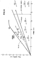
- Fig. 4 shows the preferred deposition regime for depositing the epitaxial refill in the trench structures.
- the arrow with the spurious growth label indicates region in the drawing representing conditions in which spurious growth was observed and is an undesirable region to operate in.
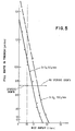
- the samples examined in this regime were deposited at the HCl 1/min flows indicated next to the data. No spurious growth was observed on samples grown at the 0.6 1/min and higher. This region of no spurious growth is indicated on both Fig. 4 and Fig. 5 and includes HC1 inputs above 0.6 1/min. Since deposition rates decrease with HC1 input as seen in Fig. 5, for filling deep trenches the preferred rate is between between 0.05 to 0.3 micrometers/minute and optimally at 0.1 micrometers/minute as also shown in Fig. 5.
- Suitable precleaning of the trenches prior to the epitaxial refill can include a post RIE cleaning followed by an 0 2 ash for 30 minutes.
- a Buffered HF exposure can be used to remove any silicon oxide which might form at room temperature.
- the trench widths on the same integrated circuit substrate may be of various widths in the range of, for example, 1 to 300 micrometers. Experiments have shown that the re-filling level of epitaxial silicon does not vary significantly for trench widths in this range with a experimental maximum nominal deviation found to be about + 10 %. Re-fills using this system contains no voids and exhibited top growth surfaces indicative of highlv-oriented single crystal growth.
- a low temperature insulator deposition forms the conformal layer 36 as seen in Fig. 2.
- This layer should be deposited to leave between about 0.5 to 1.0 micrometers of insulator over the epitaxial fill subsequent to planarization.
- One preferred material for the capping layer is tetraethylorthosilicate (TEOS) to form a silicon dioxide layer.
- TEOS tetraethylorthosilicate
- This film is deposited at 730°C in a LPCVD system optimally at below 1 torr, and N 2 is used as a carrier gas.
- the TEOS source is at 55°C (11 torr) and pumping speed controls the pressure.
- the films are densified at between 800 to 900°C for about 30 minutes in steam. For further information concerning this process reference may be made to the D.L. Burt et al., U.S. 3,934,060.
- the chemical-mechanical polishing process is varied depending upon the composition of the insulating layer 36. Where the silicon dioxide has been formed from the TEOS process the polishing may be accomplished using 6 weight percent colloidal silica with potassium hydroxide to adjust the pH to about 12.
- This slurry can be formed using colloidal silica, such as the trademarked silica sol composition "Syton HT-50" commercially available from Monsanto Company, St. Louis, Missouri, U.S.A.
- This S y ton HT-50 has a silica content of about 50 weight percent with the maximum particle size of 40 to 45 millimicrons.
- the polishing machine includes a bowl having a slurry outlet and a driven plate. Mounted on the plate by any suitable means is a soft, firm surface composed of a poromeric material, such as an artificial leather or PODELL 210 made by the Podell Inc., of Newark, Delaware, U.S.A.
- the plate is rotated by means of suitable driving means coupled through a shaft.
- the wafers to be polished are mounted on a plate opposite to the poromeric surface by means of suitable adhesive or other suitable method.
- the plate with the mounted wafers thereon is maintained against the surface with a substantial pressure applied to urge the wafers firmly against the polishing surface.
- the preferred pressure is between about 2 to 6 PSI.
- the rotation of the driven plate having the poromeric polishing material thereon produces a rotation of the plate having the wafers thereon.
- the surface of the wafers is continuously wetted with excess quantity of polishing slurry by flowing it through an opening in the rotating plate.
- a parastolic pump moves the slurry through the opening. Excess slurry is splashed from the end of the rotating plates and flows out of the excess slurry opening.
- the removal rates are about 400 nm/per minute. Where a silicon nitride layer is utilized as a stop layer the ratio of polishing is 10 to 1 in favor of silicon dioxide over silicon nitride.
- the chemical-mechanical polishing mechanism is not fully understood. However, it is believed that the surface of the silicon dioxide is hydrolyzed by the slurry and the poromeric surface wipes off this by hydrolyzed material at the high points on the wafers until a stop layer such as Si 3 N 4 is reached.
- the Si 3 N 4 material is not polished as fast as silicon dioxide with this slurry and pH conditions.
- the polishing ratio is about 10 Si0 2 to 1 S i 3 N 4 .
- the epitaxial refills obtained and measured for the data summarized in Fig. 4 and Fig. 5 were grown at 1000°C at near atmospheric pressure using SiCl4-H2 with and without HCl as indicated on the plot.
- the epitaxial refills were deposited in an AMC 7800 reactor manufactured by Applied Materials, Santa Clara, California. B 2 H 6 was employed as a dopant.
- the SiCl 4 input was 10.2 g/min. in a H 2 flow of 120 1/min (liters per minute).
- Fill level vs. time are plotted for a number of cases, for the above conditions, with and without HC1. Spurious growth was observed for the epitaxial refills where no HCI was employed whereas no spurious growth occurred for the refills wherein 0.6 1/min HCl was employed.
- the trench was filled to 1.5 nanometers from the top surface of the silicon wafer.
- a low temperature silicon dioxide layer of 2.0 nanometers was blanket deposited over the surface having the trench.
- the deposition used TEOS at 730°C in a low pressure chemical vapor deposition system.
- the silicon dioxide layer was then densified by heating it in steam at 800°C for 30 minutes.
- the TEOS-deposited silicon dioxide layer was polished back to remove all of the silicon dioxide on the surface of the wafer.
- the result is a filled trench with the silicon dioxide capping layer.
- the polishing was accomplished by using a 6 weight % colloidal silica slurry which had a pH of 12. The pH was adjusted with KOH.
- the wafer to be polished was fixed to one plate.
- a IC-40 poromeric surface produced by Podell Inc. of Newark, Delaware was mounted on a second plate. The poromeric surface was firmly urged against the wafer with a pressure of 3 p si.
- the p oromeric surface carried plate was also driven to cause rotation which in turn produces a rotation of the plate carrying the wafer.
- the surface of the wafer was continuously wetted with excess quantity of polishing slurry by flowing it through a central opening in the rotating plate.
- the silicon dioxide layer above the trench was removed at a rate of 400 nanometers/minute.
- HC1 flow was varied from 0 - 5 1/min in separate experiments.
- HC1 inputs between 0 and 0.5 1/min yielded spurious growth.
- Marked reduction in spurious growth occurred between HCl inputs of above 0.5 1/min and 0.6 1/min where the growth was eliminated.
- spurious growth was not observed for values above 0.6 1/min the deposition rates became unsuitably low, for values greater than 1.4 1/min (0.05 ⁇ m/min) for very deep trench filling.
- the deposition condition at approximately 1.0 - 1.4 1/min of HC1 appear optimum for reducing spurious growth as well as providing flat, nearly facetless refills at a suitable rate of fill.
- the most optimum value is between about 1.1 - 1.2 1/min HC1.
Abstract
Description
- The present invention is concerned with methods for filling trenches in semiconductor substrates so as to form void free patterns of isolation within the substrate. In particular, the process and resulting structure is involved in forming a pattern of isolation in a semiconductor substrate wherein the isolation includes epitaxial semiconductor material and a low temperature, chemical vapor deposited insulator thereover.
- In the monolithic integrated circuit technology, it is usually necessary to isolate various active and passive elements from one another within the integrated circuit structure. These devices have been isolated by back biasing PN junctions, partial dielectric isolation and complete dielectric isolation. The dielectric materials used have been silicon dioxide and the like. The preferred isolation for these active and passive devices is some form of dielectric isolation. The dielectric isolation has the substantial advantage over PN junction isolation because it allows the butting of circuit elements against the isolation and thereby result in greater density of packing of the active and passive devices in the integrated circuitry.
- A form of dielectric isolation is disclosed in the H.B. Pogge U.S. Patent 4,256,514. Pogge describes isolation refill techniques employed in deep trench isolation formation wherein chemical vapor deposition or the like is used to deposit insulating material such as, silicon dioxide or polycrystalline silicon into the pattern of trenches. Such systems involve a homogeneous gas phase reaction wherein the silicon dioxide, polycrystalline silicon or the like is formed in the gas from the reactive species present and is deposited therefrom onto the surfaces and into the pattern of trenches. The problem with this method of deposition is that there is a tendency to form voids within the trench patterns particularly where trenches cross one another. Also, the refilling deposition can produce structurally deficient or loosely packed material which mav not be the best isolation structures in integrated circuits. The presence of voids and this loose structure have a tendency to magnify the formation of defects in silicon areas which are later to serve as active or passive device regions.
- The L.M. Ephrath et al., Patent Application Serial No. 393,997 filed 6/30/82 (YO 9-81-069) assigned to the same assignee as the present invention describes another dielectric isolation method and resulting structure wherein the pattern of trenches is filled with void-free polycrystalline silicon or epitaxial silicon. Ephrath et al., utilize a sidewall composed of insulating material with or without a nucleating material thereover.°The bottom of the trench pattern is open to the monocrystalline semiconductor body such as silicon. Epitaxial silicon is then grown from the bottom opening of the monocrystalline silicon bodv and perpendicular from the sidewall surfaces containing the nucleating material. While the result of this epitaxial growth is a void free-structure, there are sharp facets near the top of the insulating sidewall, where no nucleating material is used. The epitaxial layer filling grows from the substrate. The epitaxial layer and substrate is typically monocrystalline silicon. This is also illustrated in N. Endo et al., "Novel Device Isolation Technology with Selective Epitaxial Growth" IEDM Tech. Digest p. 241, San Francisco Meeting Dec. 13-15, 1982. Where a nucleating layer of, for example, polycrystalline silicon is used over the insulating sidewall only a small epitaxial layer filling and mostly polycrystalline semiconductor layer results. A void is usually formed in the structure in deeper structures (about 4 µm) required for isolation than those employed by N. Endo et al.
- Selective epitaxial growth on monocrystalline silicon areas has been accomplished by workers in the field with reduced polycrystalline silicon growth on masking insulator layers on the surface of the monocrystalline silicon substrate. W.A.P. Claassen et al., in "The Nucleation of CVD Silicon on SiO2 and Si3N4 Substrates" J. Electrochem. Soc.: Solid - State Science and Technology, Vol. 128, No. 6, pp. 1353-1359 describes in a theoretical way epitaxial growth of silicon using a SiH4-HCl-H2, system. Hans Kürten et al., in "Selective Low-Pressure Silicon Epitaxy for MOS and Bipolar Transistor Application" in IEEE Transactions on Electron Devices, Vol. ED-30, No. 11, November 1983, pp. 1511-1515 and H.J. Voss, et al., in "Device Isolation Technology By Selective Low-Pressure Silicon Epitaxy" IEDM December 1983, paper 2.5 pp. 35-38 teaches that it is impossible to obtain flat surfaces at atmospheric pressure and deposition conditions when using a SiH2Cl2-HCl-H2 system. The papers further indicates that operation of the system lower then 1060°C at 760 torr or 1 atmosphere deposition cannot produce satisfactory results. The papers show experimentally that one must operate at low pressures, of the order of 40 torr and temperatures of the order of 950°C using a SiH2Cl2 system. The IEEE Transactions on Electron Devices article references the P. Rai-Choudhury et al., article in J. Electrochem. Soc. Solid State Science and Technology, May 1973, pp. 664-668 is cited by Kürten et al to show that very significant and undesirable faceting is produced at atmospheric deposition conditions. Kürten et al., teaches that the low pressure and lower temperature conditions are required to overcome these undesirable conditions. In N. Endo et al., in "CMOS Technology Using SEG Isolation Technique" in IEDM 1983, paper number 2.4, pp. 31-34; and N. Endo et al., in "Novel Device Isolation Technology with Selective Epitaxial Growth" in IEDM 1982, paper number 9.7, pp. 241-244; and K. Tanno et al., in "Selective Silicon Epitaxy Using Reduced Pressure Technique" in Japanese Journal of Applied Physics, Vol. 21, No. 9, September 1982, pp. L564-L566 describe lcw pressure epitaxial deposition similar to the above cited Kürten et al., papers. They also use the SiH2Cl2-HCl-H2 system. These papers utilize polysilicon on the sidewall of patterned silicon dioxide layer to obtain flat surfaces as seen in the N. Endo et al., IEDM 1982, pp. 243 Fig. 3A and 3B.
- The invention as claimed is intended to provide a method for forming void-free, deep isolation structures in monocrvstalline semiconductor bodies. The key problem to be overcome in this process is the spurious growth of polycrystalline silicon on a surface insulating layer during epitaxial silicon growth within the pattern of trenches.
- There is contained within a semiconductor body a pattern of substantially vertically sided trenches. The pattern of isolation trenches isolate regions of monocrvstalline semiconductor material which may contain active and passive semiconductor devices. The depth of the pattern of trenches is greater than about 3 micrometers. A first insulating layer is located upon the sidewalls of the trenches. The base or bottom of the trenches is open to the monocrystalline semiconductor body. An epitaxial layer extending from the base of the trenches fills the pattern of trenches up to between about 0.5 micrometers to 1.5 micrometers from the upper surface of the trenches. A capping second insulating layer fills the additional portion of the pattern of trenches above the upper surfaces of the epitaxial layer for isolation of the pattern of trenches from the ambient. It is the dense epitaxial monocrystalline semiconductor which prevents the formation of voids within the pattern of trenches. The epitaxial layer must be grown in such a way so as no spurious growth occurs upon the principal surfaces of the substrate, because such growth would prevent the satisfactory chemical-mechanical polishing of the C.V.D. insulator layer.
- The methods for forming void-free, deep isolation patterned structure in a semiconductor body such as, monocrystalline silicon proceeds by first forming substantially vertically sided pattern of trenches having an insulating layer sidewall and open bottom to the monocrystalline silicon body. The depth of the pattern of trenches is greater than about 3 micrometers. Monocrystalline silicon is epitaxially grown in the trenches from the monocrystalline silicon bottom to form a dense void-free trench structure up to about 0.5 micrometers to 1.5 micrometers from the top of the trench structure. A SiC14-H2-HCl gaseous reaction system is used at a pressure of about 1 atmosphere and temperature between about 900 to 1100°C. These process conditions prevents the formation of spurious polycrystalline silicon growth upon surface insulating layers while accomplishing the filling of the deep pattern of isolation trenches in a rapid manner. A insulating capping layer of such as, silicon dioxide is utilized to isolate the pattern of trenches from the ambient. This is accomplished by the chemical vapor deposition (CVD) of the insulating layer and the chemical-mechanical polishing is employed for removal of the insulating layer above the top surface of the pattern of trenches.
- One way of carrying out the invention is described in detail below with reference to drawings in which
- Figs. 1 illustrate the process of the present
- through 3 invention for forming a void-free isolation structure in a monocrystalline semiconductor body,
- Fig. 4 is a graphical representation showing the relationship of fill level versus time where HC1 is used in the SiCl4-H2 system and where HC1 is not used, and
- Fig. 5 is a graphical representation showing the relationship of fill rate vs. HC1 input for two SiCl4 inputs.
- Referring now more particularly to Fig. 1, there is shown a
semiconductor body 12 of a P- conductivity type. The semiconductor body is typically <100> crystallographically oriented silicon and of a resistivity in the order of 1 to 20 ohm-cm. Conventional lithography and etching techniques are utilized to form the mask for the subcollector diffusion step. N type impurities are then diffused by conventional techniques to form a region having a surface concentration level of typically 5 x 10²⁰ atoms/cc. The N type impurity may be, for example, arsenic or antimony. The structure is now subjected to a thermal oxidation to form silicon dioxide thereover. Simultaneously with the growth of the silicon dioxide, the N type impurity is driven further into the semiconductor body. If it were desired to form a PNP transistor rather than an NPN transistor, opposite conductivity types are utilized as is well understood by those skilled in the art. - The silicon dioxide layer on the surface of the silicon body is removed by use of conventional etching techniques. The silicon body is then placed in an epitaxial growth chamber and a monocrystalline silicon layer is grown upon the principal surface of the silicon body having the N+ diffusions therein. This growth is done by conventional techniques such as the use of SiCl4/H2; SiH2Cl2/H2 or SiH4/H2 mixtures at growth temperatures of about 1000°C to 1200°C. The thickness of the epitaxial layer is typically 1.5 micrometers but may be in the range`of 0.5 to 5 micrometers. During the epitaxial growth the epitaxial layer is doped with an N- type impurity of a low concentration level which is typically 2 x 10¹⁶ atoms/cc. During the epitaxial growth, the N+ region outdiffuses into the epitaxial layer to fully form the
final N+ region 14 as illustrated in Fig. 1. The remaining portions of theepitaxial layer 16 will be N- doped. Theregion 14 will be connected as the subcollector of the NPN transistor as is understood by those skilled in the art. - An insulating
layer 20 is formed upon the principal surface of the substrate. It may be a composite of several layers. For example a silicon dioxide layer may be formed by conventional techniques of either thermal growth at a temperature of about 970°C in wet or dry oxygen ambient or by chemical vapor deposition. A silicon nitride layer may be formed thereover typically by a chemical vapor deposition. A second silicon dioxide layer may be formed by chemical vapor deposition over the silicon nitride layer. A resist layer (not shown) is deposited over the insulating layer. - This insulating layer is then formed into a mask using conventional lithography techniques so that openings are provided in the desired pattern of isolation trenches planned. The
layer 20 is etched using conventional chemical, reactive ion etching or plasma etching techniques at the openings of resist layer down to the monocrystalline silicon substrate. - The substrate is now ready to utilize the
layer 20 as the mask for the trench formation following the removal of the resist layer from the surface oflayer 20. This process must be accomplished using anisotropic reactive ion etching (RIE) which produces substantially vertical sidewalls for the trenches. The trench depth for bipolar device isolation is at least 3 micrometers and preferably 4.0 to 7.0 micrometers. One suitable example of forming the trenches by RIE is the use of carbontetrafluoride (CF4) gas. Other suitable examples of gases include CC14-Ar and C12-Ar. Details of the RIE are described in the co-pending patent application of J.M. Harvilchuck et al., Serial No. 960,322, filed November 13, 1978, which is a continuation of patent application Serial No. 822,775, filed August 8, 1975, now abandoned and the J.A. Bondur et al., U.S. 4,104,086 and assigned to the same assignee as the assignee of this invention. - An
insulator layer 28 of, for example, silicon dioxide is preferably formed by thermal oxidation in steam at a temperature of about 970°C on the surface of the trenches. Thelayer 28 of silicon dioxide may alternatively be formed by chemical vapor deposition but this would necessitate the removal of the deposited silicon dioxide from thelayer 20 surface. The preferred thickness of thelayer 28 of the silicon dioxide is preferably in the range of 50 to 500 nanometers. It may be also desirable to form a composite layer of silicon dioxide and silicon nitride layer as insulatinglayer 28 on the surface of the substrate. This silicon nitride laver can be deposited by conventional chemical vapor deposition techniques. An additional SiO, layer may be then deposited by CVD techniques, such as TEOS. - The
layer 28 is removed from the base of the trench pattern by anisotropic etch such as reactive ion etching. - Next,
monocrystalline semiconductor layer 18, typically silicon is epitaxially grown in the pattern of trenches from the monocrystalline semiconductor bottom of the trench. The method of growing silicon is by a gas-solid or heterogeneous reaction system. The heterogeneous reaction system desirably includes hydrogen, silicon and chlorine. The particularlv preferred system is a combination of gases including SiCl4, H2, HC1 and the P+ dopant B2H6. The epitaxial growth trench filling process is carried out at temperature of between about 900°C to 1100°C and preferably about 1000°C to provide a sufficiently fast filling of the trenches. This is highly preferable when a bipolar pattern of trench isolation is being formed, because of the substantial depth of the trenches. The dopant concentration of B2H6 or the like is between about 1 x 10 19 a/cc to 3 x 10²⁰a/cc to provide a epitaxial filling material having a resistivity of about 0.01 to 0.005 ohm-cm. Subsequent heating of this structure produces aP+ region 32 in the substrate to form one portion of the isolation structure. The P+ dopant is used where NPN transistors are to be formed. Where PNP devices are to be formed, opposite conductivities are used as is understood by one skilled in the art. The epitaxial layer extends from the base of the pattern of trenches up to between about 0.5 to 1.5 from the upper top surface of the pattern of trenches. The resulting structure is shown in Fig. 1. - Fig. 4 shows the preferred deposition regime for depositing the epitaxial refill in the trench structures. The arrow with the spurious growth label indicates region in the drawing representing conditions in which spurious growth was observed and is an undesirable region to operate in. The samples examined in this regime were deposited at the
HCl 1/min flows indicated next to the data. No spurious growth was observed on samples grown at the 0.6 1/min and higher. This region of no spurious growth is indicated on both Fig. 4 and Fig. 5 and includes HC1 inputs above 0.6 1/min. Since deposition rates decrease with HC1 input as seen in Fig. 5, for filling deep trenches the preferred rate is between between 0.05 to 0.3 micrometers/minute and optimally at 0.1 micrometers/minute as also shown in Fig. 5. The higher rate can be obtained bv increasing the SiCl4 input as shown in Fig. 5. Suitable precleaning of the trenches prior to the epitaxial refill can include a post RIE cleaning followed by an 02 ash for 30 minutes. A Buffered HF exposure can be used to remove any silicon oxide which might form at room temperature. - The trench widths on the same integrated circuit substrate may be of various widths in the range of, for example, 1 to 300 micrometers. Experiments have shown that the re-filling level of epitaxial silicon does not vary significantly for trench widths in this range with a experimental maximum nominal deviation found to be about + 10 %. Re-fills using this system contains no voids and exhibited top growth surfaces indicative of highlv-oriented single crystal growth.
- A low temperature insulator deposition forms the
conformal layer 36 as seen in Fig. 2. This layer should be deposited to leave between about 0.5 to 1.0 micrometers of insulator over the epitaxial fill subsequent to planarization. One preferred material for the capping layer is tetraethylorthosilicate (TEOS) to form a silicon dioxide layer. This film is deposited at 730°C in a LPCVD system optimally at below 1 torr, and N2 is used as a carrier gas. The TEOS source is at 55°C (11 torr) and pumping speed controls the pressure. The films are densified at between 800 to 900°C for about 30 minutes in steam. For further information concerning this process reference may be made to the D.L. Burt et al., U.S. 3,934,060. - A Fig. 2 structure now is to be polished using a chemical-mechanical polishing process to remove the
insulator layer 36 from above the pattern of trenches. The chemical-mechanical polishing process is varied depending upon the composition of the insulatinglayer 36. Where the silicon dioxide has been formed from the TEOS process the polishing may be accomplished using 6 weight percent colloidal silica with potassium hydroxide to adjust the pH to about 12. This slurry can be formed using colloidal silica, such as the trademarked silica sol composition "Syton HT-50" commercially available from Monsanto Company, St. Louis, Missouri, U.S.A. This Syton HT-50 has a silica content of about 50 weight percent with the maximum particle size of 40 to 45 millimicrons. The polishing machine includes a bowl having a slurry outlet and a driven plate. Mounted on the plate by any suitable means is a soft, firm surface composed of a poromeric material, such as an artificial leather or PODELL 210 made by the Podell Inc., of Newark, Delaware, U.S.A. The plate is rotated by means of suitable driving means coupled through a shaft. The wafers to be polished are mounted on a plate opposite to the poromeric surface by means of suitable adhesive or other suitable method. The plate with the mounted wafers thereon is maintained against the surface with a substantial pressure applied to urge the wafers firmly against the polishing surface. The preferred pressure is between about 2 to 6 PSI. The rotation of the driven plate having the poromeric polishing material thereon produces a rotation of the plate having the wafers thereon. The surface of the wafers is continuously wetted with excess quantity of polishing slurry by flowing it through an opening in the rotating plate. A parastolic pump moves the slurry through the opening. Excess slurry is splashed from the end of the rotating plates and flows out of the excess slurry opening. The removal rates are about 400 nm/per minute. Where a silicon nitride layer is utilized as a stop layer the ratio of polishing is 10 to 1 in favor of silicon dioxide over silicon nitride. - The chemical-mechanical polishing mechanism is not fully understood. However, it is believed that the surface of the silicon dioxide is hydrolyzed by the slurry and the poromeric surface wipes off this by hydrolyzed material at the high points on the wafers until a stop layer such as Si3N4 is reached. The Si3N4 material is not polished as fast as silicon dioxide with this slurry and pH conditions. The polishing ratio is about 10 Si02 to 1 Si3 N 4.
- The following EXAMPLE is included merely to aid in the understanding of the invention and variations may be made by one skilled in the art without departing from the spirit and scope of the invention.
- The epitaxial refills obtained and measured for the data summarized in Fig. 4 and Fig. 5 were grown at 1000°C at near atmospheric pressure using SiCl4-H2 with and without HCl as indicated on the plot. The epitaxial refills were deposited in an AMC 7800 reactor manufactured by Applied Materials, Santa Clara, California. B2H6 was employed as a dopant. The SiCl4 input was 10.2 g/min. in a H2 flow of 120 1/min (liters per minute). Fill level vs. time are plotted for a number of cases, for the above conditions, with and without HC1. Spurious growth was observed for the epitaxial refills where no HCI was employed whereas no spurious growth occurred for the refills wherein 0.6 1/min HCl was employed.
- The trench was filled to 1.5 nanometers from the top surface of the silicon wafer. A low temperature silicon dioxide layer of 2.0 nanometers was blanket deposited over the surface having the trench. The deposition used TEOS at 730°C in a low pressure chemical vapor deposition system. The silicon dioxide layer was then densified by heating it in steam at 800°C for 30 minutes.
- The TEOS-deposited silicon dioxide layer was polished back to remove all of the silicon dioxide on the surface of the wafer. The result is a filled trench with the silicon dioxide capping layer. The polishing was accomplished by using a 6 weight % colloidal silica slurry which had a pH of 12. The pH was adjusted with KOH. The wafer to be polished was fixed to one plate. A IC-40 poromeric surface produced by Podell Inc. of Newark, Delaware was mounted on a second plate. The poromeric surface was firmly urged against the wafer with a pressure of 3 psi. The poromeric surface carried plate was also driven to cause rotation which in turn produces a rotation of the plate carrying the wafer. The surface of the wafer was continuously wetted with excess quantity of polishing slurry by flowing it through a central opening in the rotating plate. The silicon dioxide layer above the trench was removed at a rate of 400 nanometers/minute.
- HC1 flow was varied from 0 - 5 1/min in separate experiments. HC1 inputs between 0 and 0.5 1/min yielded spurious growth. Marked reduction in spurious growth occurred between HCl inputs of above 0.5 1/min and 0.6 1/min where the growth was eliminated. Although spurious growth was not observed for values above 0.6 1/min the deposition rates became unsuitably low, for values greater than 1.4 1/min (0.05 µm/min) for very deep trench filling. At HC1 inputs above 2.3 1/min etching rather than deposition occurred making this an unsuitable region. (Data not shown). The deposition condition at approximately 1.0 - 1.4 1/min of HC1 appear optimum for reducing spurious growth as well as providing flat, nearly facetless refills at a suitable rate of fill. The most optimum value is between about 1.1 - 1.2 1/min HC1.
Claims (9)
Applications Claiming Priority (2)
| Application Number | Priority Date | Filing Date | Title |
|---|---|---|---|
| US624320 | 1984-06-25 | ||
| US06/624,320 US4526631A (en) | 1984-06-25 | 1984-06-25 | Method for forming a void free isolation pattern utilizing etch and refill techniques |
Publications (2)
| Publication Number | Publication Date |
|---|---|
| EP0166121A2 true EP0166121A2 (en) | 1986-01-02 |
| EP0166121A3 EP0166121A3 (en) | 1989-06-28 |
Family
ID=24501530
Family Applications (1)
| Application Number | Title | Priority Date | Filing Date |
|---|---|---|---|
| EP85105248A Ceased EP0166121A3 (en) | 1984-06-25 | 1985-04-30 | Integrated circuit isolation structure and method of making it |
Country Status (3)
| Country | Link |
|---|---|
| US (1) | US4526631A (en) |
| EP (1) | EP0166121A3 (en) |
| JP (1) | JPS6113641A (en) |
Families Citing this family (48)
| Publication number | Priority date | Publication date | Assignee | Title |
|---|---|---|---|---|
| US4528047A (en) * | 1984-06-25 | 1985-07-09 | International Business Machines Corporation | Method for forming a void free isolation structure utilizing etch and refill techniques |
| US4680614A (en) * | 1984-06-25 | 1987-07-14 | Beyer Klaus D | Planar void free isolation structure |
| US4693783A (en) * | 1984-12-31 | 1987-09-15 | Gte Laboratories Incorporated | Method of producing interconnections in a semiconductor integrated circuit structure |
| US4795679A (en) * | 1985-05-22 | 1989-01-03 | North American Philips Corporation | Monocrystalline silicon layers on substrates |
| US4660278A (en) * | 1985-06-26 | 1987-04-28 | Texas Instruments Incorporated | Process of making IC isolation structure |
| US4714520A (en) * | 1985-07-25 | 1987-12-22 | Advanced Micro Devices, Inc. | Method for filling a trench in an integrated circuit structure without producing voids |
| US5462767A (en) * | 1985-09-21 | 1995-10-31 | Semiconductor Energy Laboratory Co., Ltd. | CVD of conformal coatings over a depression using alkylmetal precursors |
| US4789648A (en) * | 1985-10-28 | 1988-12-06 | International Business Machines Corporation | Method for producing coplanar multi-level metal/insulator films on a substrate and for forming patterned conductive lines simultaneously with stud vias |
| US4944836A (en) * | 1985-10-28 | 1990-07-31 | International Business Machines Corporation | Chem-mech polishing method for producing coplanar metal/insulator films on a substrate |
| US4745081A (en) * | 1985-10-31 | 1988-05-17 | International Business Machines Corporation | Method of trench filling |
| KR900003618B1 (en) * | 1986-05-30 | 1990-05-26 | 후지쓰가부시끼가이샤 | Semiconductor device |
| US4835741A (en) * | 1986-06-02 | 1989-05-30 | Texas Instruments Incorporated | Frasable electrically programmable read only memory cell using a three dimensional trench floating gate |
| US4981813A (en) * | 1987-02-24 | 1991-01-01 | Sgs-Thomson Microelectronics, Inc. | Pad oxide protect sealed interface isolation process |
| US4906585A (en) * | 1987-08-04 | 1990-03-06 | Siemens Aktiengesellschaft | Method for manufacturing wells for CMOS transistor circuits separated by insulating trenches |
| US4822755A (en) * | 1988-04-25 | 1989-04-18 | Xerox Corporation | Method of fabricating large area semiconductor arrays |
| EP0417197A4 (en) * | 1988-05-17 | 1992-07-08 | Xicor, Inc | Deposited tunneling oxide |
| US5219774A (en) * | 1988-05-17 | 1993-06-15 | Xicor, Inc. | Deposited tunneling oxide |
| US4894352A (en) * | 1988-10-26 | 1990-01-16 | Texas Instruments Inc. | Deposition of silicon-containing films using organosilicon compounds and nitrogen trifluoride |
| US5188987A (en) * | 1989-04-10 | 1993-02-23 | Kabushiki Kaisha Toshiba | Method of manufacturing a semiconductor device using a polishing step prior to a selective vapor growth step |
| US5108946A (en) * | 1989-05-19 | 1992-04-28 | Motorola, Inc. | Method of forming planar isolation regions |
| US5017999A (en) * | 1989-06-30 | 1991-05-21 | Honeywell Inc. | Method for forming variable width isolation structures |
| US5234861A (en) * | 1989-06-30 | 1993-08-10 | Honeywell Inc. | Method for forming variable width isolation structures |
| US5173439A (en) * | 1989-10-25 | 1992-12-22 | International Business Machines Corporation | Forming wide dielectric-filled isolation trenches in semi-conductors |
| US5094972A (en) * | 1990-06-14 | 1992-03-10 | National Semiconductor Corp. | Means of planarizing integrated circuits with fully recessed isolation dielectric |
| US5192706A (en) * | 1990-08-30 | 1993-03-09 | Texas Instruments Incorporated | Method for semiconductor isolation |
| US5102809A (en) * | 1990-10-11 | 1992-04-07 | Texas Instruments Incorporated | SOI BICMOS process |
| US5262354A (en) * | 1992-02-26 | 1993-11-16 | International Business Machines Corporation | Refractory metal capped low resistivity metal conductor lines and vias |
| US5300813A (en) * | 1992-02-26 | 1994-04-05 | International Business Machines Corporation | Refractory metal capped low resistivity metal conductor lines and vias |
| US5494857A (en) * | 1993-07-28 | 1996-02-27 | Digital Equipment Corporation | Chemical mechanical planarization of shallow trenches in semiconductor substrates |
| US5346584A (en) * | 1993-07-28 | 1994-09-13 | Digital Equipment Corporation | Planarization process for IC trench isolation using oxidized polysilicon filler |
| US5994718A (en) * | 1994-04-15 | 1999-11-30 | National Semiconductor Corporation | Trench refill with selective polycrystalline materials |
| US5492858A (en) * | 1994-04-20 | 1996-02-20 | Digital Equipment Corporation | Shallow trench isolation process for high aspect ratio trenches |
| US5738800A (en) * | 1996-09-27 | 1998-04-14 | Rodel, Inc. | Composition and method for polishing a composite of silica and silicon nitride |
| US6132637A (en) | 1996-09-27 | 2000-10-17 | Rodel Holdings, Inc. | Composition and method for polishing a composite of silica and silicon nitride |
| US6180480B1 (en) | 1998-09-28 | 2001-01-30 | International Business Machines Corporation | Germanium or silicon-germanium deep trench fill by melt-flow process |
| US6403412B1 (en) | 1999-05-03 | 2002-06-11 | International Business Machines Corp. | Method for in-situ formation of bottle shaped trench by gas phase etching |
| DE10063491A1 (en) * | 2000-12-20 | 2002-06-27 | Bayer Ag | Sour polishing slurry for chemical mechanical polishing of SiO¶2¶ insulation layers |
| KR20020053560A (en) * | 2000-12-27 | 2002-07-05 | 박종섭 | Method for forming a separation film of a semi-conductor device |
| KR20020056659A (en) * | 2000-12-29 | 2002-07-10 | 박종섭 | Method for forming element isolating film of semicoductor device |
| KR100383758B1 (en) * | 2000-12-29 | 2003-05-14 | 주식회사 하이닉스반도체 | Method of forming an isolation layer in a semiconductor device |
| KR20030000134A (en) * | 2001-06-22 | 2003-01-06 | 주식회사 하이닉스반도체 | Forming method for field oxide of semiconductor device |
| KR100475025B1 (en) * | 2002-10-25 | 2005-03-10 | 주식회사 하이닉스반도체 | Forming method for field oxide of semiconductor device |
| US7531395B2 (en) * | 2004-09-01 | 2009-05-12 | Micron Technology, Inc. | Methods of forming a layer comprising epitaxial silicon, and methods of forming field effect transistors |
| US8673706B2 (en) * | 2004-09-01 | 2014-03-18 | Micron Technology, Inc. | Methods of forming layers comprising epitaxial silicon |
| US7132355B2 (en) * | 2004-09-01 | 2006-11-07 | Micron Technology, Inc. | Method of forming a layer comprising epitaxial silicon and a field effect transistor |
| US7144779B2 (en) * | 2004-09-01 | 2006-12-05 | Micron Technology, Inc. | Method of forming epitaxial silicon-comprising material |
| US7109097B2 (en) * | 2004-12-14 | 2006-09-19 | Applied Materials, Inc. | Process sequence for doped silicon fill of deep trenches |
| US7679130B2 (en) * | 2005-05-10 | 2010-03-16 | Infineon Technologies Ag | Deep trench isolation structures and methods of formation thereof |
Citations (9)
| Publication number | Priority date | Publication date | Assignee | Title |
|---|---|---|---|---|
| JPS56146249A (en) * | 1980-04-14 | 1981-11-13 | Fujitsu Ltd | Semiconductor device |
| JPS57106121A (en) * | 1980-12-24 | 1982-07-01 | Hitachi Ltd | Ion implanting method |
| JPS5839026A (en) * | 1981-09-02 | 1983-03-07 | Nippon Telegr & Teleph Corp <Ntt> | Semiconductor device and manufacture thereof |
| EP0073370A2 (en) * | 1981-08-27 | 1983-03-09 | International Business Machines Corporation | Integrated circuit structure and method for forming a recessed isolation structure for integrated circuits |
| JPS58207652A (en) * | 1982-05-28 | 1983-12-03 | Fujitsu Ltd | Manufacture of semiconductor device |
| EP0107902A2 (en) * | 1982-09-29 | 1984-05-09 | Fujitsu Limited | A method for fabricating isolation regions in semiconductor devices |
| JPS59129439A (en) * | 1983-01-14 | 1984-07-25 | Nec Corp | Manufacture of substrate for semiconductor device |
| US4528047A (en) * | 1984-06-25 | 1985-07-09 | International Business Machines Corporation | Method for forming a void free isolation structure utilizing etch and refill techniques |
| EP0155698A2 (en) * | 1984-03-23 | 1985-09-25 | Nec Corporation | A method for manufacturing a semiconductor integrated circuit device provided with an improved isolation structure |
Family Cites Families (14)
| Publication number | Priority date | Publication date | Assignee | Title |
|---|---|---|---|---|
| US3661636A (en) * | 1970-04-22 | 1972-05-09 | Ibm | Process for forming uniform and smooth surfaces |
| JPS5120266B2 (en) * | 1972-04-03 | 1976-06-23 | ||
| US3934060A (en) * | 1973-12-19 | 1976-01-20 | Motorola, Inc. | Method for forming a deposited silicon dioxide layer on a semiconductor wafer |
| US3969168A (en) * | 1974-02-28 | 1976-07-13 | Motorola, Inc. | Method for filling grooves and moats used on semiconductor devices |
| JPS51135385A (en) * | 1975-03-06 | 1976-11-24 | Texas Instruments Inc | Method of producing semiconductor device |
| US4104086A (en) * | 1977-08-15 | 1978-08-01 | International Business Machines Corporation | Method for forming isolated regions of silicon utilizing reactive ion etching |
| US4256514A (en) * | 1978-11-03 | 1981-03-17 | International Business Machines Corporation | Method for forming a narrow dimensioned region on a body |
| US4255207A (en) * | 1979-04-09 | 1981-03-10 | Harris Corporation | Fabrication of isolated regions for use in self-aligning device process utilizing selective oxidation |
| JPS566449A (en) * | 1979-06-28 | 1981-01-23 | Chiyou Lsi Gijutsu Kenkyu Kumiai | Production of semiconductor device |
| US4309716A (en) * | 1979-10-22 | 1982-01-05 | International Business Machines Corporation | Bipolar dynamic memory cell |
| JPS56137647A (en) * | 1980-03-31 | 1981-10-27 | Chiyou Lsi Gijutsu Kenkyu Kumiai | Semiconductor and its manufacture |
| JPS5851533A (en) * | 1981-09-24 | 1983-03-26 | Hitachi Ltd | Manufacture of semiconductor device |
| JPS58192346A (en) * | 1982-05-06 | 1983-11-09 | Toshiba Corp | Manufacture of semiconductor device |
| US4473598A (en) * | 1982-06-30 | 1984-09-25 | International Business Machines Corporation | Method of filling trenches with silicon and structures |
-
1984
- 1984-06-25 US US06/624,320 patent/US4526631A/en not_active Expired - Lifetime
-
1985
- 1985-02-08 JP JP60022139A patent/JPS6113641A/en active Granted
- 1985-04-30 EP EP85105248A patent/EP0166121A3/en not_active Ceased
Patent Citations (9)
| Publication number | Priority date | Publication date | Assignee | Title |
|---|---|---|---|---|
| JPS56146249A (en) * | 1980-04-14 | 1981-11-13 | Fujitsu Ltd | Semiconductor device |
| JPS57106121A (en) * | 1980-12-24 | 1982-07-01 | Hitachi Ltd | Ion implanting method |
| EP0073370A2 (en) * | 1981-08-27 | 1983-03-09 | International Business Machines Corporation | Integrated circuit structure and method for forming a recessed isolation structure for integrated circuits |
| JPS5839026A (en) * | 1981-09-02 | 1983-03-07 | Nippon Telegr & Teleph Corp <Ntt> | Semiconductor device and manufacture thereof |
| JPS58207652A (en) * | 1982-05-28 | 1983-12-03 | Fujitsu Ltd | Manufacture of semiconductor device |
| EP0107902A2 (en) * | 1982-09-29 | 1984-05-09 | Fujitsu Limited | A method for fabricating isolation regions in semiconductor devices |
| JPS59129439A (en) * | 1983-01-14 | 1984-07-25 | Nec Corp | Manufacture of substrate for semiconductor device |
| EP0155698A2 (en) * | 1984-03-23 | 1985-09-25 | Nec Corporation | A method for manufacturing a semiconductor integrated circuit device provided with an improved isolation structure |
| US4528047A (en) * | 1984-06-25 | 1985-07-09 | International Business Machines Corporation | Method for forming a void free isolation structure utilizing etch and refill techniques |
Non-Patent Citations (8)
| Title |
|---|
| IBM TECHNICAL DISCLOSURE BULLETIN, vol. 23, no. 1, June 1980, pages 171-172, New York, US; J.S. LECHATON et al.: "Process for forming a deep substrate contact" * |
| IBM TECHNICAL DISCLOSURE BULLETIN, vol. 25, no. 11A, April 1983, pages 5672-5673, New York, US; B. EL-KAREH et al.: "Bipolar one-device random-access memory cell" * |
| INTERNATIONAL ELECTRONIC DEVICES MEETING 1983, IEEE; New York, US; H.-J. VOSS et al.: "Device isolation technology by selective low-pressure silicon epitaxy" * |
| PATENT ABSTRACTS OF JAPAN, vol. 6, no. 25 (E-94)[903], 13th February 1982; & JP-A-56 146 249 (FUJITSU K.K.) 13-11-1981 * |
| PATENT ABSTRACTS OF JAPAN, vol. 7, no. 119 (E-177)[1264], 24th May 1983; & JP-A-58 39 026 (NIPPON DENSHIN DENWA KOSHA) 07-03-1983 * |
| PATENT ABSTRACTS OF JAPAN, vol. 8, no. 226 (E-272)[1663], 17th October 1984; & JP-A-57 106 121 (FUJITSU K.K.) 19-06-1984 * |
| PATENT ABSTRACTS OF JAPAN, vol. 8, no. 256 (E-280)[1693], 22nd November 1984; & JP-A-59 129 439 (NIPPON DENKI K.K.) 25-07-1984 * |
| PATENT ABSTRACTS OF JAPAN, vol. 8, no. 53 (E-231)[1490], 9th March 1894; & JP-A-58 207 652 (FUJITSU K.K.) 03-12-1983 * |
Also Published As
| Publication number | Publication date |
|---|---|
| JPS6113641A (en) | 1986-01-21 |
| JPH0586660B2 (en) | 1993-12-13 |
| EP0166121A3 (en) | 1989-06-28 |
| US4526631A (en) | 1985-07-02 |
Similar Documents
| Publication | Publication Date | Title |
|---|---|---|
| US4526631A (en) | Method for forming a void free isolation pattern utilizing etch and refill techniques | |
| US4689656A (en) | Method for forming a void free isolation pattern and resulting structure | |
| US4528047A (en) | Method for forming a void free isolation structure utilizing etch and refill techniques | |
| US4758531A (en) | Method of making defect free silicon islands using SEG | |
| US4473598A (en) | Method of filling trenches with silicon and structures | |
| US5192708A (en) | Sub-layer contact technique using in situ doped amorphous silicon and solid phase recrystallization | |
| US5234535A (en) | Method of producing a thin silicon-on-insulator layer | |
| EP0071204B1 (en) | Method for forming recessed dielectric isolation | |
| EP0036111B1 (en) | Method for making fine deep dielectric isolation | |
| Goulding | The selective epitaxial growth of silicon | |
| US6114219A (en) | Method of manufacturing an isolation region in a semiconductor device using a flowable oxide-generating material | |
| US7482210B2 (en) | Method of fabricating semiconductor device having junction isolation insulating layer | |
| JPS62269335A (en) | Manufacture of semiconductor device | |
| US4900689A (en) | Method of fabrication of isolated islands for complementary bipolar devices | |
| EP0405923B1 (en) | Method for forming variable width isolation structures | |
| US4680614A (en) | Planar void free isolation structure | |
| CA1208805A (en) | Vertically isolated complementary transistors | |
| US6194286B1 (en) | Method of etching thermally grown oxide substantially selectively relative to deposited oxide | |
| US4649630A (en) | Process for dielectrically isolated semiconductor structure | |
| US6673696B1 (en) | Post trench fill oxidation process for strained silicon processes | |
| US3736193A (en) | Single crystal-polycrystalline process for electrical isolation in integrated circuits | |
| US6228733B1 (en) | Non-selective epitaxial depostion technology | |
| JPS61229317A (en) | Formation of semiconductor cell and integrated circuit | |
| JPH07183370A (en) | Manufacture of semiconductor device | |
| KR20010005151A (en) | Isolation using chemical mechanical polishing |
Legal Events
| Date | Code | Title | Description |
|---|---|---|---|
| PUAI | Public reference made under article 153(3) epc to a published international application that has entered the european phase |
Free format text: ORIGINAL CODE: 0009012 |
|
| AK | Designated contracting states |
Designated state(s): DE FR GB |
|
| 17P | Request for examination filed |
Effective date: 19860424 |
|
| PUAL | Search report despatched |
Free format text: ORIGINAL CODE: 0009013 |
|
| AK | Designated contracting states |
Kind code of ref document: A3 Designated state(s): DE FR GB |
|
| 17Q | First examination report despatched |
Effective date: 19910311 |
|
| STAA | Information on the status of an ep patent application or granted ep patent |
Free format text: STATUS: THE APPLICATION HAS BEEN REFUSED |
|
| 18R | Application refused |
Effective date: 19920326 |
|
| RIN1 | Information on inventor provided before grant (corrected) |
Inventor name: SILVESTRI, VICTOR JOSEPH Inventor name: TANG, D. DUAN-LEE |