EP0166225A2 - High yield liquid crystal display and method of making same - Google Patents
High yield liquid crystal display and method of making same Download PDFInfo
- Publication number
- EP0166225A2 EP0166225A2 EP85106417A EP85106417A EP0166225A2 EP 0166225 A2 EP0166225 A2 EP 0166225A2 EP 85106417 A EP85106417 A EP 85106417A EP 85106417 A EP85106417 A EP 85106417A EP 0166225 A2 EP0166225 A2 EP 0166225A2
- Authority
- EP
- European Patent Office
- Prior art keywords
- electrode
- subassembly
- isolation
- diode
- further characterized
- Prior art date
- Legal status (The legal status is an assumption and is not a legal conclusion. Google has not performed a legal analysis and makes no representation as to the accuracy of the status listed.)
- Granted
Links
Images


Classifications
-
- G—PHYSICS
- G09—EDUCATION; CRYPTOGRAPHY; DISPLAY; ADVERTISING; SEALS
- G09G—ARRANGEMENTS OR CIRCUITS FOR CONTROL OF INDICATING DEVICES USING STATIC MEANS TO PRESENT VARIABLE INFORMATION
- G09G3/00—Control arrangements or circuits, of interest only in connection with visual indicators other than cathode-ray tubes
- G09G3/006—Electronic inspection or testing of displays and display drivers, e.g. of LED or LCD displays
-
- G—PHYSICS
- G02—OPTICS
- G02F—OPTICAL DEVICES OR ARRANGEMENTS FOR THE CONTROL OF LIGHT BY MODIFICATION OF THE OPTICAL PROPERTIES OF THE MEDIA OF THE ELEMENTS INVOLVED THEREIN; NON-LINEAR OPTICS; FREQUENCY-CHANGING OF LIGHT; OPTICAL LOGIC ELEMENTS; OPTICAL ANALOGUE/DIGITAL CONVERTERS
- G02F1/00—Devices or arrangements for the control of the intensity, colour, phase, polarisation or direction of light arriving from an independent light source, e.g. switching, gating or modulating; Non-linear optics
- G02F1/01—Devices or arrangements for the control of the intensity, colour, phase, polarisation or direction of light arriving from an independent light source, e.g. switching, gating or modulating; Non-linear optics for the control of the intensity, phase, polarisation or colour
- G02F1/13—Devices or arrangements for the control of the intensity, colour, phase, polarisation or direction of light arriving from an independent light source, e.g. switching, gating or modulating; Non-linear optics for the control of the intensity, phase, polarisation or colour based on liquid crystals, e.g. single liquid crystal display cells
- G02F1/133—Constructional arrangements; Operation of liquid crystal cells; Circuit arrangements
- G02F1/136—Liquid crystal cells structurally associated with a semi-conducting layer or substrate, e.g. cells forming part of an integrated circuit
- G02F1/1362—Active matrix addressed cells
- G02F1/13624—Active matrix addressed cells having more than one switching element per pixel
-
- G—PHYSICS
- G06—COMPUTING; CALCULATING OR COUNTING
- G06F—ELECTRIC DIGITAL DATA PROCESSING
- G06F11/00—Error detection; Error correction; Monitoring
- G06F11/07—Responding to the occurrence of a fault, e.g. fault tolerance
- G06F11/16—Error detection or correction of the data by redundancy in hardware
- G06F11/20—Error detection or correction of the data by redundancy in hardware using active fault-masking, e.g. by switching out faulty elements or by switching in spare elements
-
- G—PHYSICS
- G09—EDUCATION; CRYPTOGRAPHY; DISPLAY; ADVERTISING; SEALS
- G09G—ARRANGEMENTS OR CIRCUITS FOR CONTROL OF INDICATING DEVICES USING STATIC MEANS TO PRESENT VARIABLE INFORMATION
- G09G3/00—Control arrangements or circuits, of interest only in connection with visual indicators other than cathode-ray tubes
- G09G3/20—Control arrangements or circuits, of interest only in connection with visual indicators other than cathode-ray tubes for presentation of an assembly of a number of characters, e.g. a page, by composing the assembly by combination of individual elements arranged in a matrix no fixed position being assigned to or needed to be assigned to the individual characters or partial characters
- G09G3/34—Control arrangements or circuits, of interest only in connection with visual indicators other than cathode-ray tubes for presentation of an assembly of a number of characters, e.g. a page, by composing the assembly by combination of individual elements arranged in a matrix no fixed position being assigned to or needed to be assigned to the individual characters or partial characters by control of light from an independent source
- G09G3/36—Control arrangements or circuits, of interest only in connection with visual indicators other than cathode-ray tubes for presentation of an assembly of a number of characters, e.g. a page, by composing the assembly by combination of individual elements arranged in a matrix no fixed position being assigned to or needed to be assigned to the individual characters or partial characters by control of light from an independent source using liquid crystals
-
- H—ELECTRICITY
- H01—ELECTRIC ELEMENTS
- H01L—SEMICONDUCTOR DEVICES NOT COVERED BY CLASS H10
- H01L23/00—Details of semiconductor or other solid state devices
- H01L23/52—Arrangements for conducting electric current within the device in operation from one component to another, i.e. interconnections, e.g. wires, lead frames
- H01L23/522—Arrangements for conducting electric current within the device in operation from one component to another, i.e. interconnections, e.g. wires, lead frames including external interconnections consisting of a multilayer structure of conductive and insulating layers inseparably formed on the semiconductor body
- H01L23/525—Arrangements for conducting electric current within the device in operation from one component to another, i.e. interconnections, e.g. wires, lead frames including external interconnections consisting of a multilayer structure of conductive and insulating layers inseparably formed on the semiconductor body with adaptable interconnections
- H01L23/5256—Arrangements for conducting electric current within the device in operation from one component to another, i.e. interconnections, e.g. wires, lead frames including external interconnections consisting of a multilayer structure of conductive and insulating layers inseparably formed on the semiconductor body with adaptable interconnections comprising fuses, i.e. connections having their state changed from conductive to non-conductive
- H01L23/5258—Arrangements for conducting electric current within the device in operation from one component to another, i.e. interconnections, e.g. wires, lead frames including external interconnections consisting of a multilayer structure of conductive and insulating layers inseparably formed on the semiconductor body with adaptable interconnections comprising fuses, i.e. connections having their state changed from conductive to non-conductive the change of state resulting from the use of an external beam, e.g. laser beam or ion beam
-
- H—ELECTRICITY
- H01—ELECTRIC ELEMENTS
- H01L—SEMICONDUCTOR DEVICES NOT COVERED BY CLASS H10
- H01L2924/00—Indexing scheme for arrangements or methods for connecting or disconnecting semiconductor or solid-state bodies as covered by H01L24/00
- H01L2924/0001—Technical content checked by a classifier
- H01L2924/0002—Not covered by any one of groups H01L24/00, H01L24/00 and H01L2224/00
-
- Y—GENERAL TAGGING OF NEW TECHNOLOGICAL DEVELOPMENTS; GENERAL TAGGING OF CROSS-SECTIONAL TECHNOLOGIES SPANNING OVER SEVERAL SECTIONS OF THE IPC; TECHNICAL SUBJECTS COVERED BY FORMER USPC CROSS-REFERENCE ART COLLECTIONS [XRACs] AND DIGESTS
- Y10—TECHNICAL SUBJECTS COVERED BY FORMER USPC
- Y10S—TECHNICAL SUBJECTS COVERED BY FORMER USPC CROSS-REFERENCE ART COLLECTIONS [XRACs] AND DIGESTS
- Y10S359/00—Optical: systems and elements
- Y10S359/90—Methods
Definitions
- the present invention relates generally to light influencing displays, such as liquid crystal displays, and to methods of increasing the manufacturing yield of such displays.
- Light influencing displays may be used advantageously in many applications.
- one form of light influencing displays namely liquid crystal displays, are extensively used in calculators, digital watches, digital clocks, and very small television displays.
- Each pixel usually includes two electrodes formed on spaced apart substrates with the liquid crystal material located between the electrodes.
- the liquid crystal material located between the electrodes.
- a transmissive or a reflective display can be formed.
- Electrodes To control a display, selected electrical potentials are applied across the electrodes.
- the electrodes in turn impress a field onto the liquid crystal material causing it to take a desired orientation, thereby forming the transmissive or reflective display.
- Each pixel In order to form a complex display a substantial number of pixels is necessary. Each pixel must be addressable, usually by means of x and y address lines. Further, experience has shown that it is very desirable when using nematic liquid crystal display material to alternate the polarity of the potentials applied to the electrodes for the purpose of extending the life of the display material.
- isolation devices such as diodes or transistors are often used in connection with each electrode.
- a display has, for example, 1,000 pixels, at least 1,000 operative isolation devices must be formed on the substrate. It is well known that in the manufacture of integrated or thin film semiconductor devices that a certain percentage of the devices which are formed will be defective for various reasons. Because of the failure rate in forming isolation devices, pixels in a display can be unusable due to inoperative isolation devices. Thus, the ability to test a display quickly to determine if it is usable is important.
- the present invention provides for a subassembly for use in making a display of a type that incorporates a light influencing material.
- One such material is nematic liquid crystal display material.
- the subassembly has a substrate on which are formed one or more coplanar, spaced apart electrodes.
- the subassembly also includes one or more isolation devices coupled to respective electrodes. Addressing means are provided for enabling the selective application of electrical potentials to each isolation device to enable the selective testing thereof.
- the subassembly can also include redundant isolation devices which can be used to replace defective isolation devices and to enable the selective application of driving potentials across the pairs of electrodes for operating the display.
- the invention also provides for a switching element coupled in series with each redundant isolation device. By applying radiant energy thereto the switching device will change from a relatively low conductivity state to a relatively high conductivity state coupling the redundant isolation device to the respective electrode.
- the switching element, or antifuse can be formed of an energy sensitive chalcogenide or a fusable amorphous semiconductor alloy.
- the invention also provides for a display of a type that includes a light influencing material.
- the display includes a plurality of pixels with each pixel having a pair of spaced apart electrodes with light influencing material positioned there between.
- One type of material that can be used is a conventional nematic liquid crystal display material.
- One or more isolation devices is coupled to respective pixel electrodes. Addressing means are provided for enabling the selective application of electrical potentials to each isolation device to enable the selective testing thereof.
- a subassembly is provided that incorporates self-selecting redundancy.
- a redundant isolation structure is formed with parallel branches including at least one isolation element, such as a diode, in each branch.
- One form of self-selecting redundancy includes at least two series connected diodes in each branch.
- a second form includes a diode in series with a thin-film fuse in each branch. The thin film fuse is vaporized by a current that flows therethrough in the event the series connected diode is short circuited.
- the invention also provides for a method of making and testing a subassembly for a display including the steps of providing a substrate, forming a plurality of spaced apart electrodes on the substrate, forming one or more isolation devices each coupled to a respective electrode, and applying electrical potentials to each isolation device individually to test the operation thereof.
- the method can further include the steps of forming one or more redundant isolation devices, uncoupling each inoperative isolation device and coupling selected redundant isolation devices to respective electrodes as replacements.
- the method can further include using electrical or radiant energy to uncouple inoperative isolation devices and using electrical or radiant energy to electrically couple replacement isolation devices to respective pixel electrodes.
- the method can further include forming diodes or transistors as isolation devices and redundant isolation devices.
- the method can further include forming a subassembly for a display by providing a substrate, forming a first electrode on the substrate, forming an isolation device electrically coupled to the pixel electrode, forming a first address line electrically coupled to the isolation device and a second address line coupled to the electrode than applying selected electric potentials between the first and second address lines to test the electrical connectivity therebetween and the operation of the isolation device.
- the method also provides for forming a subassembly for a display with self-selecting redundancy.
- the method includes forming an electrode, as well as forming isolation means and redundant isolation means including means for selecting the redundant isolation means in the event of a failure of the isolation means.
- Figs. 1 through 6 illustrate an embodiment of the present invention.
- Figs. 7 and 8 illustrate several additional alternate embodiments of the invention.
- Figs. 9 through 14 illustrate yet another embodiment of the invention.
- Fig. 1 is a partly diagrammatic, partly schematic view of a subassembly 5 of a display embodying the present invention.
- a liquid crystal display is disclosed.
- the invention is applicable to any display incorporating a light influencing material as defined below.
- Fig. 2 is a view in section taken along line 2-2' of Fig. 1 of the subassembly 5 incorporated into a pixel 7 of a liquid crystal display.
- the subassembly 5 for one pixel 7 is illustrated, it can be appreciated that many such subassemblies can be formed in, for example, a row and column matrix to provide a two-dimensional display.
- the subassembly 5 is formed on an transparent insulating substrate 10, such as glass.
- a pair of address lines 12, 14 which cross one another at an insulated cross-over 16.
- address line 12 Connected to address line 12 is an isolation diode 18 and connected to address line 14 is an isolation diode 20.
- the diodes 18 and 20 are each connected to an electrode segment 22 which is illustrated in a substantially rectangular shape.
- the isolation diodes 18 and 20 in combination with the address lines 12 and 14 can be used to address the electrode segment 22 when the subassembly 5 is being tested or under normal operating conditions.
- the address lines 12, 14, the diodes 18, 20 and the electrode segment 22 are connected electrically in series. Because of the series connection it is possible to apply voltages to the address lines 12 and 14 during the manufacturing process to test the operation of the diodes 18 and 20. Additionally, in view of the fact that the electrode segment 22 is in series with the diodes 18 and 20 this testing also tests the electrical continuity between the address lines 12 and 14 and the electrode segment 22 when the diodes 18 and 20 are forward biased.
- redundant isolation structure 24 which includes series connected diodes 26, 28.
- the diodes 26, 28 are connected in parallel with the diode 18 between the address line 12 and the pixel electrode 22.
- a second redundant isolation structure 30 formed of series connected diodes 32, 34 is connected between the address line 14 and the pixel electrode 22 in parallel with the diode 20.
- the isolation structures 24, 30 are formed as far away from the respective diodes 18, 20 as possible to minimize the possibility of a dual failure due to a common mechanical cause such as a grain of dust on the substrate 10.
- the redundant isolation device structures 24 and 30 can be used to replace the diodes 18 and 20.
- the diodes 26 and 34 are switching elements that can be removed from the circuit if it is necessary to use the redundant isolation diodes 28 and 32.
- Diodes 18 and 20 can be disconnected from the electrode 22 by directing radiant energy, such as from a laser or other high intensity light source at connection points such as 19a or 19b associated with diode 18 as well as connection points 21a or 21b associated with the diode 20.
- the high intensity radiant energy directed at the points 19 and 21 will vaporize previously deposited metal contacts thereby isolating the diode 18 and the diode 20 from the pixel electrode 22.
- breakdown voltages can be applied across t'he address lines 12 and 14 to cause diode 26 and diode 34 to break down and short circuit. After the breakdown potentials are applied the diodes 28 and 32 can then be used as alternate isolation devices when addressing the electrode 22. Diodes 26 and 34 are switches or isolation devices which keep diodes 28 and 32 respectively disconnected from the electrode 22 until diodes 26 and 34 are shorted. If the potential to the address lines 12 and 14 is reversed, the resultant addressing isolation devices become 26 and 34 instead of 28 and 32.
- Optical energy, from a laser can also be used to heat and fuse or short circuit the switching diodes 26, 34 instead of using potentials applied to the address lines 12, 14 to short circuit those diodes
- short circuit refers to a switching element such as the diode 26 assuming a high conductivity, low resistance state so as to permit a corresponding isolation diode 28 to be used to address element 22.
- short circuit can also include a direct metal-to-metal connection.
- a second pair of address lines 36, 38 which is connected by isolation diodes 40, 42 to a second electrode segment 44 also formed on the substrate 10.
- the electrode segment 44 is coplanar with and laterally spaced apart from the electrode segment 22.
- Redundant isolation structures 46 and 48 are connected respectively between the address line 36 and the electrode segment 44 and between the address line 38 and the electrode segment 44.
- the redundant isolation structures 46 and 48 are used in precisely the same way as are the previously discussed redundant isolation structures 24, 30.
- a third electrode segment or common electrode 50 is formed on a second substrate 52 (not shown in Fig. 1) spaced apart from the first substrate 10. Between the substrates 10 and 52 is a region 54 which can be filled with a light influencing material 56.
- the material 56 can, for example, be a standard nematic liquid crystal material.
- light influencing material is meant any material which emits light or can be used to selectively vary the intensity, phase, or polarization of light either being reflected from or transmitted through the material. Liquid crystal material is only one such material having these characteristics.
- Fig. 2 illustrates the physical relationships between the substrates 10, 52 and the electrode segments 22, 44 and 50 of the pixel 7.
- the redundant diode structures 30, 46 are shown schematically connected in parallel with the isolation diodes 18, 40.
- the electrode segment 50 is shown formed on the substrate 52 with the region 54 between the electrodes 22, 44 and 50 filled with the liquid crystal material 56.
- Figs. 1 and 2 The pixel structure illustrated in Figs. 1 and 2 is particularly applicable for practicing the present invention because all of the address lines, driven electrodes, and isolation devices are formed on a single substrate.
- Such pixel structures are particularly disclosed and claimed in copending United States Patent Application Serial No. 626,133, Attorney Docket No. 722, filed concurrently herewith, for Liquid Crystal Displays and Subassemblies Having Improved Pixel Electrodes, which application is incorporated by reference herein.
- the diodes illustrated in Figs. 1 and 2 such as the isolation diode 18 or the redundant diodes 26, 28 are preferably formed from a deposited semiconductor material.
- the deposited semiconductor material is preferably an amorphous semiconductor alloy including silicon.
- the amorphous silicon alloy can also include hydrogen and/or fluorine and can be deposited by plasma assisted chemical vapor deposition i.e. glow discharge as disclosed for example in U.S. Patent No. 4,226,898 which issued on October 7, 1980 in the names of Stanford R. Ovshinsky and Arun Madan for "Amorphous Semiconductors Equivalent to Crystalline Semiconductors Produced by a Glow Discharge Process.”
- the redundant isolation structures 30, 46 can be formed as back-to-back Schottky barrier diodes sharing a common layer of amorphous silicon alloys positioned between two thin films of a high work function metal such as platinum, palladium, chromium, iridium or rhodium. Such diodes are disclosed in the '898 patent.
- the redundant diode structures 30, 46 can be formed of back-to-back semiconductor diodes with a common intrinsic semiconductor layer between two similarly doped semiconductor layers such as are disclosed in pending United States Patent Application Attorney Docket No. 747, filed April 25, 1984, entitled "Programmable Semiconductor Switch for a Display Matrix or the Like and Method of Making Same," assigned to the Assignee of the present invention. The disclosure of the 747 application is hereby incorporated by reference.
- One particular advantage of the pixel 7 is the ability to quickly test the subassembly 5 which is inherent in that structure. As discussed above, during the testing procedure the application of an electrical potential across the address lines 12, 14 makes it possible to test the operation and the electrical conductivity of the series combination formed of the address line 12, diode 18, electrode segment 22, diode 20 and address line 14. A similar test sequence can be run with respect to the electrode segment 44. Hence, if a subassembly 5 is first formed including all of the structure on the substrate 10 it is possible to thoroughly test that subassembly and replace defective isolation devices with the available redundant devices such as 26 or 32 before the substrate 52 is ever attached to the substrate 10.
- the test sequence can be performed at a much faster rate than a complete display can be tested.
- the ability to quickly test the structure of the substrate 10 and to replace non-functional isolation devices is especially important from a manufacturing point of view.
- One of the most difficult problems encountered in the manufacture of devices such as liquid crystal displays is the random failure of isolation elements.
- the structure of Figs. 1 and 2 provides a solution to this problem.
- Fig. 3 is a top plan view of the subassembly 5 showing in more detail an exemplary structure.
- the same identification numerals are used to identify elements in Fig. 3 as were used to previously identify corresponding elements in Figs. 1 and 2.
- the isolation diode 18 (shown in dashed lines) is formed above a region of the address line 12 and beneath a section of a deposited conductor 60.
- the conductor 60 couples the diode 18 to the electrode segment 22.
- the conductor 60 can be deposited using standard deposition techniques and may be formed of a variety of metals such as aluminum, molybdenum, chromium, tantalum, tungsten, palladium and platinum.
- the conductor 60 could also be a conductive semiconductor material.
- the isolation diode 20 is formed on a region of the electrode segment 22 and is connected to the address line 14 by a deposited conductor 62.
- the conductor 62 is the same type of material as is the conductor 60.
- the diode 18 can be disconnected at point 19a or 19b of Fig. 1 after the testing sequence if it is inoperative.
- the region 19a or 19b is shown in Fig. 3 as a generalized region 19 which is near the center of the conductor 60.
- the diode 20 can be disconnected from the address line 14 by removing a part of the conductor 62.
- the disconnection can be made at the regions 19, 21 corresponding to either the anode or the cathode of the diode 18 and the diode 20 by use of a directed laser beam to vaporize the deposited conductors 60, 62 in the regions 19, 21 or by applying current through the conductors 60, 62 to vaporize them.
- Fig. 3 Shown in Fig. 3 is the redundant structure 24 which is formed with diode 28 located on a region of the address line 12 and diode 26 located on a region of the pixel electrode 22.
- the diodes 26 and 28 are interconnected by a deposited conductive layer 64 corresponding to the type of metal or material used in forming the conductor 60.
- Fig. 3 Shown in Fig. 3 is the redundant structure 30 which is formed with diode 34 located on a region of the address line 14 and diode 32 located on a region of the pixel electrode 22.
- the diodes 32 and 34 are interconnected by a deposited conductive layer 66 corresponding to the type of metal or material used in forming the conductor 60.
- the isolation diodes 40, 42 and the redundant structures 46, 48 have the same position and structure with respect to the electrode segment 44 as do the diodes 18, 20 and the redundant structures 30 and 24 with respect to the electrode segment 22.
- Connective layers 70, 72, 74 and 76 correspond in function and structure with respect to the electrode segment 44 as do the connectors 60, 62, 64 and 66 discussed above.
- An insulating layer 80 is formed on the substrate 10 and abuts the electrode segment 22 at a plurality of edges 80a.
- the insulating layer 80 overlies the electrode segment 22 adjacent the diodes 20, 26 and 32.
- the layer 80 is transparent.
- the insulating layer 80 also abuts the electrode segment 44 at a plurality of edges 80b. In the region of the diode 42 and the redundant isolation structures 46, 48, the insulating layer 80 overlies the electrode segment 44.
- the edges of overlying electrode 50 correspond to the boundary edges 80a, 80b of the insulating layer 80.
- the subassembly 5 of Fig. 3 can be tested without the spaced apart electrode segment 50 and second substrate 52 as discussed above.
- Fig. 4 is a section taken along line 4-4' of Fig. 3 and shows the detailed structure of the subassembly 5 in the region of the isolation diode 18 and the conductive layer 60.
- the electrode segment 22 is formed on the substrate 10 as a deposited layer of indium tin oxide 22a and an overlying layer of chromium 22b.
- the two layer structure 22 is transparent permitting a viewer to look through the substrate 10, into the internal region 54 where the nematic liquid crystal fluid 56 is contained.
- the address line 12 is also formed of deposited layers 12a, 12b of indium tin oxide and chromium respectively.
- the diode 18 is preferably formed from a deposited semiconductor material.
- the deposited semiconductor material is preferably an amorphous semiconductor alloy including silicon.
- the amorphous silicon alloy can also include hydrogen and/or fluorine and can be deposited by plasma assisted chemical vapor deposition i.e. glow discharge as disclosed, for example, in U.S. Patent No. 4,226,898 which is sued on October 7, 1980 in the names of Stanford R.
- the diode 18 preferably has an n-i-p configuration formed by an n-type doped region 18a, an intrinsic region 18b overlying the first doped region 18a, and a p-type doped region 18c overlying the intrinsic region 18b.
- the diode 18 can be formed more specifically by depositing the previously mentioned amorphous silicon alloy over the region of the address line 12 and thereafter selectively etching portions of the amorphous silicon alloy by utilizing a suitable mask and conventional photolithography techniques.
- the mask utilized during the etching process preferably defines a diode configuration wherein each diode is about 20 to 50 microns on a side.
- One specific diode size is 30 microns by 30 microns.
- Representative thicknesses for the amorphous silicon alloy regions 18a, b, c can be, for example, 300 to 1,000 angstroms and preferably 500 angstroms for the p-type regions, 1,000 to 10,000 angstroms and preferably 3,000 angstroms for the intrinsic regions, and 300 to 1,000 angstroms and preferably 500 angstroms for the n-type regions.
- the insulating material 80 can be formed from any deposited insulator such as silicon oxide (Si x Oy) or silicon nitride (Si x Ny), or a polyimide, for example.
- the insulating layer 80 defines an opening or via 82 to the anode 18c of the diode 18.
- the configuration of the layer 80 can be obtained by roller, extrusion, or spin coating the polyimide, for example, over the entire surface area, spin coating a layer of photoresist over the polyimide layer, and then exposing and developing out both of the photoresist and the polyimide using a further mask. This step forms the opening 82 which exposes the anode 18c of the diode 18.
- the insulating layer 80 abuts the electrode segment 22 at the surface 80a as can be seen in Fig. 4 and also in Fig. 3.
- the deposited conductive layer 60 is in contact with the anode 18c of the diode 18 and a region 84 of the electrode 22 and couples the diode 18 to electrode 22.
- the layer 60 can be deposited by means of a conventional sputtering process.
- a transparent passivating layer 86 formed, for example, from silicon dioxide covers the subassembly 5.
- the conductive layer 60 can be heated either electrically or with optical energy, such as a laser beam, at the region 19. This localized heating at the region 19 results in a localized vaporization of the conductor 60.
- Fig. 5 is a section taken along line 5-5' of Fig. 3 and discloses the structure of the redundant isolation device 30.
- the diode 32 is formed on a region of the electrode segment 22 as an n-i-p diode having layers 32a, 32b and 32c respectively out of deposited amorphous silicon alloy.
- the diode 34 is formed also as a n-i-p diode having layers 34a, b, c on a region of the address line 14.
- the insulating layer 80 supports the conductor 66 and insulates it from the subassembly 5 except at vias 88, 90.
- the conductive layer 66 is in contact with the anode 32c of the diode 32 and the anode 34c of the diode 34.
- Diodes 32, 34 are formed series coupled and in reverse relation so that normally no current will pass through the conductor 66.
- Fig. 6 is a sectional view taken along line 6-6' of Fig. 3 and discloses the structure of the isolation diode 20 with respect to the electrode segment 22.
- the diode 20 is formed of three amorphous silicon layers 20a, 20b and 20c with an n-i-p structure on a region of the electrode 22.
- the address line 14 has two layers, a layer 14a of indium tin oxide which has been deposited on the substrate 10 and a layer 14b of chromium.
- the address line 14 is transparent.
- the insulating layer 80 which was previously deposited prior to depositing the conductor 62 insulates the conductor 62 from the subassembly 5 except where vias 92 and 94 permit the conductor 60 to contact the anode 20c of diode 20 and a region of the upper layer 14b of the address line 14.
- energy for example, in the form of a laser beam, can be directed at the region 21 or an electric current can be passed through the layer 62 to locally heat the region 21 causing local vaporization of the region 19 thereby isolating the diode 20.
- the structure of the redundant diodes 26, 28 corresponds to that of the diodes 32, 34 of Fig. 5.
- the structure of the isolation diode 40 with respect to the electrode segment 44 corresponds to the previously discussed cross section of Fig. 4.
- the structures of the redundant isolation devices 46, 48 correspond to the previously discussed structure of Fig. 5.
- the structure of the diode 42 with respect to the electrode segment 44 corresponds to the previously discussed structure of Fig. 6.
- the electrode segment 50 is indicated in Fig. 3 in dashed lines as overlying the two spaced apart electrode segments 22 and 44.
- the electrode segment 50 is preferably formed of indium tin oxide deposited on the spaced apart glass substrate 52.
- the interconnection vias 82, 88, 90, 92 and 94 are also shown in dashed lines in Fig. 3. Tests as discussed above can be conducted on the subassembly 5 of Fig. 3 to determine if the isolation devices 18, 20 and 40, 42 operate properly.
- the corresponding diodes can be disconnected using localized laser induced heating and the respective pairs of redundant isolation devices 24, 30 or 46, 48 can be activated by applying a current limited breakdown voltage across the address lines to breakdown the reverse biased switching diodes, such as 28 and 34.
- the switching diodes 28 or 34 for example can be heated and fused or short circuited using laser energy.
- diodes such as 18, 20, 26 or 28 could all be formed with anodes and cathodes interchanged without departing from the spirit and scope of the present invention.
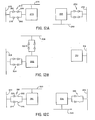
- Fig. 7 illustrates several alternate embodiments of the invention.
- electrode segments 100, 102 are addressable by address lines 104, 106; 108, 110 respectively.
- An isolation diode 112 connects the address line 104 to the electrode segment 100.
- a second isolation diode 114 connects the address line 108 to the electrode segment 102.
- the structure of Fig. 7A may also be tested prior to the completion of manufacturing and assembly using the previously disclosed method used to test the subassembly 5. Electrical potentials can be applied between the lines 104, 106 to test the diode 112 and the electrode segment 100. Potentials can be applied between the lines 108 and 110 to test the diode 114 and the electrode segment 102.
- Redundant isolation structures 116 and 118 can be included in the event either diode 112 or 114 is defective.
- the redundant isolation structures 116, 118 can be used to replace the isolation diodes 112 or 114 if necessary.
- a potential of one polarity can be applied across lines 104 and 110 and a potential of the reversible polarity can be applied across lines 108 and 106 so as to reverse the polarity applied to the nematic liquid crystal fluid in the display.
- FIG. 7B Yet another embodiment is shown in Fig. 7B.
- a pair of electrode segments 120 and 122 is shown in Fig. 7B connected respectively to address lines 124, 126 and 128.
- the address line 124 is connected to the electrode segment 120 through a diode 130.
- the address line 126 is connected to the electrode segment 120 through a diode 132.
- the structure of the address lines 124, 126, the isolation devices 130, 132 and the electrode segment 120 corresponds to the structure of the address lines 12, 14, the isolation devices 18, 20 and the electrode segment 22 of Fig. 1 and may be tested in the same way as the subassembly 5 of Fig. 1 may be tested. Additionally, if desired, redundant isolation structures 134 and 136 corresponding to redundant isolation structures 24 and 30 can be formed in parallel with the diodes 130 and 132. Under normal operating conditions the subassembly of Fig.
- 7B can be operated by applying a voltage with a first polarity between the lines 124 and 128 and a voltage of the reverse polarity between the lines 126 and 128 so as to reverse the field applied to the nematic liquid crystal material during each half frame.
- Fig. 7C illustrates yet another embodiment of the present invention.
- electrode segments 140, 142 are connected to a set of address lines 144, 146, 148 and 150 respectively.
- Address lines 144 and 146 are connected to the electrode segment 140 through thin film field effect transistors 150 and 152.
- the field effect transistors 150 and 152 are an alternate isolation device to the diodes used in the embodiments of Figs. 1, 7A and 7B.
- Connected in series with the field effect thin film transistor 150 is a thin film deposit 160.
- a similar thin film deposit 162 is connected in series between the transistor 152 and the electrode 140.
- the thin film deposits 160, 162 are switching elements preferably formed from a settable chalcogenide material which can be set (rOm a substantially non-conducting state to a substantially highly conducting state through the use of either radiant or electrical energy.
- One of the transistors 150 or 152 can be selected by setting its respective switching element 160 or 162 to a substantially highly conducting state. The respective transistor can then be tested using the lines 144, 146 and 148. If the transistor 150 is inoperative, it can be disconnected from the pixel electrode 140 by means of directed radiant energy, such as a laser beam, or by localized electrical heating used to vaporize a connection between the transistor 150 and the electrode segment 140. The redundant transistor 152 can then be selected by setting its switching element 162 to its substantially conducting state.
- the transistors 150, 152 can be deposited thin film field effect transistors of a type as disclosed in United States Patent Application Serial No. 609,640, filed May 14, 1984 entitled “Thin Film Field Effect Transistor and Method of Making Same” and assigned to the Assignee of the present invention.
- the switching elements 160, 162 can be formed of chalcogenide materials as disclosed in United States Patent No. 3,530,441 entitled “Method and Apparatus for Storing and Retrieving Information" issued September 22, 1970 and assigned to the Assignee of the present invention. The disclosure of said patent application and said issued patent are hereby incorporated by reference.
- an alternating potential can be applied across electrode segments 140, 142 by applying a selected polarity potential across the lines 146, 150 and by turning on the selected transistor 150 or 152 by a gate voltage on the line 144.
- the polarity across the lines 146, 150 can then be reversed while gate voltage is again applied to the line 144.
- the present invention includes positioning the elements 22, 44 of Fig. 1 in lateral, coplanar, spaced apart relationship as electrode segments as shown in Fig. 1 on the same substrate 10.
- the elements 22, 44 can be formed on two substrates vertically spaced apart from one another as pixel electrodes with the nematic fluid positioned therebetween.
- the elements 100, 102 can either be positioned coplanar and laterally with respect to one another on the same substrate as electrode segments or positioned in spaced apart relationship from one another as pixel electrodes with the nematic fluid located therebetween.
- the structure of Fig. 7B can also be formed in either physical relationship with the elements 120, 122 corresponding to electrode segments or pixel electrodes respectively.
- the elements 140, 142 of Fig. 7C can be formed as coplanar electrode segments or spaced apart pixel electrodes.
- Fig. 8 illustrates in more detail the embodiment of Fig. 7C discussed above.
- Fig. 8 shows in section the transistor 150 with a source region 150S formed on the address line 146, a gate electrode 150G formed on the address line 144, and a drain region 150D connected via a deposited conductor 164 to the switching element 160 formed as a deposited, settable chalcogenide material.
- the element 160 is in turn connected to the electrode segment or pixel electrode 140 by a deposited conductor 166.
- the transistor 150 is a deposited thin film field effect transistor, with an amorphous silicon layer 168 positioned between the source 150S and the drain 150D.
- An oxide layer 170 insulates the gate electrode 150G from the amorphous semiconductor material 168.
- the transistor 152 would have a similar structure.
- Fig. 9 is a top plan view of a subassembly 190 which illustrates yet another embodiment of the present invention.
- the subassembly 190 includes a transparent substrate 192 which can be formed of glass.
- a pair of transparent, coplanar, laterally spaced apart, electrode segments 194, 196 corresponding to the electrode segments 22 and 44 of Fig. 1 are formed on the substrate 192.
- First and second address lines 200, 202 are deposited on the substrate 192 as are the address lines 12 and 14 of Fig. 1 and are associated with the electrode 194.
- Address lines 204, 206 are also deposited on the substrate 192 and are associated with the electrode segment 196.
- Isolation diodes 208 and 210 formed on the address line 200 and on a region of the electrode segment 194 respectively correspond to the isolation devices 18, 20 of Fig. 1.
- a deposited conductor 209 formed of a selected metal as noted above or a doped semiconductor connects the isolation diode 208 to the electrode segment 194.
- a deposited conductor 211 formed of a selected metal as noted above or a doped semiconductor material connects the diode 210 to the address line 202.
- the redundant isolation structures 212 and 214 of the subassembly 190 each include only a single isolation diode 216 and 218 respectively.
- the diode 216 is formed on a region of the address line 200.
- the diode 216 can serve as a replacement for the diode 208.
- the diode 218 is formed on a region of the electrode segment 194 and can serve as a replacement for the diode 210.
- the diode 216 is not connected to the electrode segment 194 and the diode 218 is not connected to the address line 202.
- the address line 204 is connected to the electrode segment 196 when the subassembly 190 is manufactured by a diode 220 which is formed on a region of the electrode 196 which is in turn connected to the address line 204 by a conductor 222.
- the diode 220 corresponds in structure to the diode 210.
- the address bus 206 is connected to the electrode segment 196 when the subassembly 190 is manufactured by a diode 224 which is formed on a region of the address bus 206 and a deposited conductor 226.
- Diode 224 corresponds to the diode 208.
- the subassembly 192 is initially manufactured with a pair of redundant diodes 230 and 232 formed respectively on a region of the address line 206 and on a region of the electrode segment 196.
- the diodes 230 and 232 correspond to the redundant diodes 216 and 218.
- Diodes 230 and 232 when the substrate 190 is initially manufactured, as is the case with the respective diodes 216 and 218, are not connected to the electrode 196 or the address bus 204 respectively.
- the diodes 208, 210, 220 and 224 can be tested as discussed above by applying potentials to the address lines 200 and 202 as well as the address lines 204, 206. If any of the diode pairs 208, 210 or 222, 224 are determined by testing to be defective they may be disconnected from the electrode segments 194, 196 as discussed previously by localized heating and vaporization of the metal connecting banks 209 and 211; or 222 and 226. This corresponds to the use of laser energy to disconnect the diodes 18, 20 or 40, 42 as in Fig. 1.
- connection involves a spray and lift off type process which is well known in the art and which may be used to fabricate deposited conductors 240 and 242 which respectively connect the diode 216 to the electrode segment 194 and the diode 218 to the address line 202 or which can be used to fabricate a pair of deposited conductors 244, 246 which will connect the diode 230 to the electrode segment 196 and the diode 232 to the address line 204 respectively.
- the conductive links 240, 242 or 244, 246 may be formed by first applying a layer of positive photoresist to the subassembly 190.
- the layer of positive photoresist is exposed using a mask and developed.
- the portion of the photoresist which is exposed corresponds to those regions of the substrate 190 on which the connectors such as 240 or 242 are to be deposited.
- the exposed portion of the photoresist is removed.
- An appropriate metal or doped semiconductor is then deposited onto the substrate 190 to form a layer thereon. Metals such as aluminum, molybdenum, an alloy of molybdenum and tantalum, chromium, tantalum, tungsten, palladium or platinum may be used. After the metal has been deposited onto the exposed photoresist the excess material is removed from the substrate 190 as is well known in the art. The material that remains corresponds to the connectors 240, 242 or 244, 246.
- the cross-sectional structures of the diode 208 and the connector 209 with respect to the electrode segment 194 correspond to the structure of the diode 18 and the connector 19 of Figs. 3 and 4.
- the structures of the isolation diode 210 and the connector 211 with respect to the electrode segment 194 correspond to the structures of the diode 20 and the connector 62 of Figs. 3 and 6.
- Fig. 10 is a sectional view taken along line 10-10' of Fig. 9 which shows the structure of the redundant element 214 including the diode 218 and its related conductor or connector 242, once that connector has been deposited, with respect to the electrode segment 194.
- the electrode segment 194 is formed by depositing a layer 194a of indium tin oxide on the substrate 192. A layer of chromium 194b is then deposited on top of the indium tin oxide.
- the address line 202 is formed of a layer 202a of indium tin oxide deposited onto the substrate 192 and a layer 202b of chromium deposited on the indium tin oxide.
- the redundant isolation diode 218, is formed out of amorphous silicon alloy as discussed above with respect to the diodes 18, 20 of Fig. 1 with an n-doped layer 218a formed on the chromium layer 194b, an intrinsic layer 218b formed above and overlying the n-doped layer 218a and a p-doped layer 218c overlying the intrinsic layer 218b.
- An insulating layer 250 corresponding to the insulating layer 80 of Figs. 3 through 6 is then deposited forming vias 252 and 254 which expose regions of the address line 202 and the diode 218.
- the deposited connector 242 couples the address line 202 to the diode 218.
- a transparent passivating layer 256 corresponding to the passivating layer 86 of Figs. 4 through 6 then covers and protects the subassembly 190.
- Fig. 11 is a sectional view taken along line 11-11' of Fig. 9 and illustrates the structure of redundant element 212 including the diode 216, and associated connector 240, once that connector has been deposited, with respect to the electrode segment 194.
- the address line 200 is formed of a layer of indium tin oxide 200a deposited on the substrate 192 with a layer of chromium 200b formed thereon.
- the diode 216 is formed of amorphous silicon alloy with an n-doped region or layer 216a formed on the address line 200, an intrinsic region or layer 216 b and a p-doped region or layer 216c formed overlying the intrinsic region.
- the insulating layer 250 forms a via 260 through which the deposited metal or semiconductor 240 extends in contact with the anode 216c of the diode 216 thereby coupling it to the electrode 194.
- the passivating layer 256 is also shown in Fig. 11 covering the electronic structure.
- the structure of the diode 220 corresponds to the structure of the diode 210.
- the structure of the diode 224 corresponds to the structure of the diode 208.
- the structures of redundant diodes 230 and 232 correspond to the structures of redundant diodes 216 of Fig. 11 and 218 of Fig. 10 respectively.
- the subassembly 190 has the same advantages as does the subassembly 5 in permitting rapid testing during the manufacturing process and in providing for redundant isolation devices which can be used to replace defective isolation devices.
- the redundant isolation devices 216 and 218 of Fig. 9 have been positioned as far as possible from their corresponding primary isolation devices 208 and 210 respectively so as to minimize the chances of dual failure do to mechanical problems such as dust or other dirt having fallen on the substrate 190 during the manufacturing process.
- Fig. 12 illustrates several alternate embodiments of the present invention.
- an electrode segment 270 is connected to a redundant isolation structure 272 and to an address line 274.
- a second address line 276 is connected to the structure 272.
- the structure 272 is formed of diodes 278, 280 connected in series in the same relation and diodes 282, 284 connected in series in the same relation.
- the diodes 278, 280 are connected in parallel with the diodes 282, 284.
- the structure 272 has a self-selecting redundancy characteristic. Since diode pair 278, 280 is in parallel with diode pair 282, 284 if one of the diodes 278 or 280 is an open circuit, the diodes 282, 284 will function independently to enable the address line 276 to continue to address the electrode 270. Analogously, if diode 278 or 280 is short circuited, the other diode 280 or 278 will still function as an isolation device when the electrode 270 is not being addressed.
- a second electrode segment 286 spaced apart from the electrode 270 is connected to a third address line 288 and a second redundant structure 290.
- the structure 290 is connected to a fourth address line 292.
- the structure 290 is identical to the structure 272 and functions in the same way.
- Fig. 12B illustrates yet another embodiment of the invention with self-selecting redundancy that requires no testing.
- An electrode segment 300 is connected to first and second redundant isolation structures 302 and 304.
- the structures 302, 304 are in turn connected to address lines 306, 308 respectively.
- the structures 302, 304 are identical to and function as does the redundant isolation structure 272.
- a second electrode 310 coplanar with and spaced apart from the electrode 300 is connected to an address line 312.
- the electrodes 270 and 286 of Fig. 12A and the pair of electrodes 300, 310 of Fig. 12B can be formed as electrode segments coplanar and spaced apart from one another on a substrate.
- a third electrode such as the electrode segment 50 of Figs. 1 and 2 can be formed in spaced apart relation therewith.
- the region, such as the region 54 therebetween, can be filled with a light influencing material such as nematic liquid crystal fluid.
- the electrodes 270 and 286, or 300 and 310 can be formed as pixel electrodes on two substrates in spaced apart relation to one another with liqht influencing material therebetween.
- electrode refers to either an electrode segment or a pixel electrode.
- Fig. 12C illustrates yet another embodiment of the present invention also including self-selecting redundancy.
- An electrode 316 is connected to a redundant isolation structure 318 and to an address line 320.
- the redundant isolation structure 318 is in turn connected to an address line 322.
- the structure 318 is formed' of a diode 324 in series with a thin film fuse 326.
- the series combination of the diode 324 and fuse 326 is connected in parallel with a redundant diode 328 and fuse 330.
- the fuses 326, 330 are formed of a deposited nickel-chromium alloy.
- a second electrode 332 can be formed on the same subassembly as the electrode 316.
- the electrode 332 is connected to an address line 334 and a redundant isolation structure 336.
- the structure 336 is identical to the structure 318 and is in turn connected to an address line 338.
- redundant isolation structure 318 in normal operation, if the polarity of the address line 322 is positive with respect to the line 334 either 324 or 328 or both will be forward biased to apply a potential to the electrode 316. Hence, both diodes 324, 328 must be an open circuit to render electrode 316 inoperative. If the polarity of the line 320 is positive with respect to the line 322, as will happen in normal operation, the diodes 324 and 328 should be reverse biased.
- the structure 336 operates in the same way.
- the electrodes 316, 332 can be formed on a common substrate as coplanar spaced apart electrode segments or formed spaced apart as pixel electrodes with light influencing material therebetween.
- Fig. 12 includes self-selecting redundancy. No separate test step is necessary in the manufacture thereof.
- a typical thickness for the thin film fuses 326, 330 would be on the order of 500 angstroms to 1 micron.
- Fig. 13A illustrates yet another embodiment of the present invention.
- an electrode 350 is coupled to a redundant isolation structure 352 and an address line 354.
- the isolation structure 352 is in turn connected to a second address line 356.
- the redundant isolation structure 352 includes an isolation diode 358 which is connected in parallel with a series connected redundant isolation diode 360 and a switching device or antifuse 362.
- the switching device 362 represents a normally open circuited element or an element of low conductivity.
- the diode 358 can be disconnected from the electrode 350 by means of laser induced heating of a connection 364 between the cathode of the diode 358 and the electrode 350. Once the diode 358 has been disconnected the switching element 362 can be set or switched into its highly conducting state such that the redundant diode 360 can be used to address the electrode 350.
- a second electrode 366 is also illustrated in Fig. 13A and is connected to a redundant isolation structure 368 as well as an address line 370.
- the redundant isolation structure 368 is in turn also connected to a second address line 372.
- the redundant isolation structure 368 is identical to and functions the same as the redundant isolation structure 352.
- the electrodes 350 and 366 can be formed on a common substrate, spaced apart and essentially coplanar with one another thereby forming electrode segments which cooperate with a third common electrode segment which is spaced apart from segments 350 and 366.
- a light influencing material can be placed in the region between the common electrode and the electrode segments.
- the electrodes 350 and 366 can be used as pixel electrodes directly by forming them in spaced apart relationship with a light influencing material such as a pneumatic liquid crystal material positionable 'therebetween.
- Fig. 13B illustrates an embodiment of the switching element 362.
- the same identification numerals are used in Fig. 13B as one used in Fig. 13A to identify common elements.
- the antifuse or switching element 362 can be formed of two diodes 374, 376 series connected in reverse relation which are in turn series connected with the redundant isolation diode 360.
- the diodes 360, 374, 376 of the redundant isolation structure 352 can be formed of a deposited amorphous silicon alloy. In such an embodiment the diodes 358 and 360 will have a three layer p-i-n structure and be approximately 30 microns by 30 microns.
- the diodes 374, 376 of the switching element 362 are formed so as to be 10 microns on a side by 20 microns long. Such diodes will be on the order of 4,000 angstroms thick.
- the switching element 362 has the advantage that the diodes 374 and 376 are substantially smaller in area than either of the diodes 358 or 360. As a result, the yield will be substantially increased during the manufacturing process since the smaller cross-sectional area of the diodes 374, 376 makes them much less susceptible to having foreign matter fall thereon and produce a short circuit.
- Fig. 13C illustrates in section the structure of the diodes 374, 376.
- the diodes 374, 376 are formed on spaced apart conductors 379a, b and each has an anode 374a, 376a indicated as a p-type region in contact therewith.
- the cathodes 374b, 376b of the diodes 374, 376 are interconnected by a deposited metal layer 378.
- the diodes 374, 376 are formed as p-i-n diodes at the same time as the diodes 358 and 360 are formed. In the event that it determined that the diode 358 is not operational.
- Radiant energy in the form of a laser beam can be used to heat and vaporize the connection 364 disconnecting the diode 358 from the electrode 350.
- the laser beam can also be used to heat and fuse the diode 376, and if desired the diode 374, thereby coupling the diode 360 to the electrode element 350.
- the advantage of forming the dual diode structure 374, 376 is that no additional processing steps will be necessary to create the diodes 374, 376. Further, because of the smaller size of the diodes 374, 376 as discussed above, the manufacturing yield will be increased.
- Fig. 14A illustrates yet another form of switching element 362.
- the switching element 362 is formed of an antifuse 380.
- Fig. 14B illustrates one embodiment of the antifuse 380.
- the antifuse 380 shown in Fig. 14B is formed on deposited metal contacts 380a and 380b as a three layer 382, 384, 386 p-i-n amorphous silicon resistive element.
- the antifuse 380 of Fig. 14B exhibits a high resistivity, on the order of 10 ohms per centimeter. If the diode 358 is functioning correctly, the deposited metal connectors 380a and 380b are connected through the high resistance, low conductivity p-type amorphous silicon layer 382.
- the p-type layer 382 is about 500 angstroms thick.
- the space between the conductors 380a and 380b is on the order of 10 microns as is the overlap of the layer 382 on the conductors 380a and 380b.
- the element 380 can be deposited during the manufacturing process when the diodes 358 and 360 are being deposited and will require no additional steps. In the event that the diode 358 is defective it may be disconnected from the electrode 350 by means of radiant energy vaporizing the connection 364 as discussed above. Subsequently, the element 380 can be fused by radiant energy, such as by a laser directed thereat and its resistivity will be reduced to .1 to 1 ohm per centimeter.
- the entire three level structure 382 through 386 becomes a conductor connecting the elements 380a and 380b together. This results in 6 orders of magnitude difference in the resistance between the elements 380a and 380b before fusing as opposed to the resistance after fusing.
- Fig. 14C illustrates another embodiment of the antifuse 380.
- a p-i-n diode having 3 layers, 390 through 394 is formed on the metallic conductor 380B.
- a top metal layer 396 is formed on the diode structure 390 through 394.
- a silicon dioxide layer 398 insulates the adjacent metal conductor 380a from the four layer structure 390 through 396 as well as the metal conductor 380b.
- the anti-fuse 380 element of Fig. 14C can be fused by radiant energy, such by a laser thereby connecting the metal conductor 380a to the conductor 380b.
- the three layer diode structure 390 through 394 again has the advantage that it may be formed during the same processing operations as are used to form the diodes 358 and 360.
- Fig. 14D illustrates yet another embodiment of the switching element 380.
- the deposited metal conductors 380a and 380b are separated by an approximately 10 micron interval wherein is deposited a settable chalcogenide material 390.
- the material 390 can be set from its low conductivity state to its high conductivity state thereby connecting the diode 360 to the electrode 350.
- Chalcogenide materials of the type disclosed in the '441 patent referenced above may be used as the element 390.
- Fig. 14E illustrates a vertical form of the switching element 380.
- a silicon dioxide layer 392 or other equivalent insulator is formed on the conductor 380b.
- a via 394 is formed in the insulating layer 392.
- Chalcogenide material 396 is deposited in the via 394 and contacts the conductor 380b.
- the second metal conductor 380a is deposited over the insulating layer 392 and the settable chalcogenide layer 396.
- the chalcogenide element 396 can be set to its high conductivity state from its low conductivity state by the application of radiant energy such as by a laser beam directed thereon.
- the diodes can be formed from deposited semiconductor materials other than amorphous semiconductor alloys.
- the diodes can be formed of polycrystalline semiconductor diodes as can the isolation transistors.
- the amorphous semiconductor alloy diodes can be formed from other material configurations than the p-i-n or n-i-p configuration described herein.
- the diodes can be formed in a stacked or tandem configuration.
- the scope of the invention includes all types of transistors that can be deposited and which will provide the proper isolation characteristics.
- the scope of the invention includes the use of all types of light influencing materials as discussed herein.
Abstract
Description
- The present invention relates generally to light influencing displays, such as liquid crystal displays, and to methods of increasing the manufacturing yield of such displays.
- Light influencing displays may be used advantageously in many applications. For example, one form of light influencing displays, namely liquid crystal displays, are extensively used in calculators, digital watches, digital clocks, and very small television displays.
- Conventional liquid crystal displays include a plurality of pixels arranged in rows and columns. Each pixel usually includes two electrodes formed on spaced apart substrates with the liquid crystal material located between the electrodes. Depending upon the optical properties of the material, either a transmissive or a reflective display can be formed.
- To control a display, selected electrical potentials are applied across the electrodes. The electrodes in turn impress a field onto the liquid crystal material causing it to take a desired orientation, thereby forming the transmissive or reflective display. In order to form a complex display a substantial number of pixels is necessary. Each pixel must be addressable, usually by means of x and y address lines. Further, experience has shown that it is very desirable when using nematic liquid crystal display material to alternate the polarity of the potentials applied to the electrodes for the purpose of extending the life of the display material. To increase the isolation between pixels, isolation devices such as diodes or transistors are often used in connection with each electrode. In view of the large number of isolation devices needed, at least one per electrode, it is desirable to form them on the substrate adjacent the respective display electrode. Exemplary displays of this type are disclosed in United States Patent Application Serial No. 573,004, entitled "Liquid Crystal Displays Operated by Amorphous Silicon Alloy Diodes," filed January 23, 1984 and assigned to the Assignee of the present invention.
- If a display has, for example, 1,000 pixels, at least 1,000 operative isolation devices must be formed on the substrate. It is well known that in the manufacture of integrated or thin film semiconductor devices that a certain percentage of the devices which are formed will be defective for various reasons. Because of the failure rate in forming isolation devices, pixels in a display can be unusable due to inoperative isolation devices. Thus, the ability to test a display quickly to determine if it is usable is important.
- The present invention provides for a subassembly for use in making a display of a type that incorporates a light influencing material. One such material is nematic liquid crystal display material. The subassembly has a substrate on which are formed one or more coplanar, spaced apart electrodes. The subassembly also includes one or more isolation devices coupled to respective electrodes. Addressing means are provided for enabling the selective application of electrical potentials to each isolation device to enable the selective testing thereof. The subassembly can also include redundant isolation devices which can be used to replace defective isolation devices and to enable the selective application of driving potentials across the pairs of electrodes for operating the display.
- The invention also provides for a switching element coupled in series with each redundant isolation device. By applying radiant energy thereto the switching device will change from a relatively low conductivity state to a relatively high conductivity state coupling the redundant isolation device to the respective electrode. The switching element, or antifuse, can be formed of an energy sensitive chalcogenide or a fusable amorphous semiconductor alloy.
- The invention also provides for a display of a type that includes a light influencing material. The display includes a plurality of pixels with each pixel having a pair of spaced apart electrodes with light influencing material positioned there between. One type of material that can be used is a conventional nematic liquid crystal display material. One or more isolation devices is coupled to respective pixel electrodes. Addressing means are provided for enabling the selective application of electrical potentials to each isolation device to enable the selective testing thereof.
- A subassembly is provided that incorporates self-selecting redundancy. A redundant isolation structure is formed with parallel branches including at least one isolation element, such as a diode, in each branch. One form of self-selecting redundancy includes at least two series connected diodes in each branch. A second form includes a diode in series with a thin-film fuse in each branch. The thin film fuse is vaporized by a current that flows therethrough in the event the series connected diode is short circuited.
- The invention also provides for a method of making and testing a subassembly for a display including the steps of providing a substrate, forming a plurality of spaced apart electrodes on the substrate, forming one or more isolation devices each coupled to a respective electrode, and applying electrical potentials to each isolation device individually to test the operation thereof. The method can further include the steps of forming one or more redundant isolation devices, uncoupling each inoperative isolation device and coupling selected redundant isolation devices to respective electrodes as replacements.
- The method can further include using electrical or radiant energy to uncouple inoperative isolation devices and using electrical or radiant energy to electrically couple replacement isolation devices to respective pixel electrodes. The method can further include forming diodes or transistors as isolation devices and redundant isolation devices. The method can further include forming a subassembly for a display by providing a substrate, forming a first electrode on the substrate, forming an isolation device electrically coupled to the pixel electrode, forming a first address line electrically coupled to the isolation device and a second address line coupled to the electrode than applying selected electric potentials between the first and second address lines to test the electrical connectivity therebetween and the operation of the isolation device.
- The method also provides for forming a subassembly for a display with self-selecting redundancy. The method includes forming an electrode, as well as forming isolation means and redundant isolation means including means for selecting the redundant isolation means in the event of a failure of the isolation means.
-
- Figure 1 is a partially diagrammatic, partially schematic view of an embodiment of the invention;
- Figure 2 is a section taken along line 2-2' of Figure 1;
- Figure 3 is a top plan view of a subassembly of a liquid crystal display embodying the present invention;
- Figure 4 is a sectional view taken along line 4-4' of Figure 3;
- Figure 5 is a sectional view taken along line 5-5' of Figure 3;
- Figure 6 is a sectional view taken along line 6-6' of Figure 3;
- Figure 7A is a partly diagrammatic, partly schematic view of an alternate embodiment of the present invention;
- Figure 7B is a partly diagrammatic, partly schematic diagram of an alternate embodiment of the present invention;
- Figure 7C is a partly diagrammatic, partly schematic view of yet another alternate embodiment of the present invention;
- Figure 8 is a view in section of the structure of one of the isolation devices of Figure 7C;
- Figure 9 is a top plan view of a subassembly of a liquid crystal display of another embodiment of the present invention;
- Figure 10 is a sectional view taken along line 10-10' of Figure 9;
- Figure 11 is a sectional view taken along line 11-11' of Figure 9;
- Figure 12A is a partly diagrammatic, partly schematic view of an alternate embodiment of the present invention;
- Figure 12B is a partly diagrammatic, partly schematic view of an alternate embodiment of the present invention; and
- Figure 12C is a partly diagrammatic, partly schematic view of an alternate embodiment of the present invention.
- Figure 13A is a partly diagrammatic, partly schematic view of an alternate embodiment of the present invention.
- Figure 13B is a partly diagrammatic, partly schematic view of an alternate embodiment of the present invention.
- Figure 13C is a view in section of the switching element of Fig. 13B.
- Figure 14A is a partly diagrammatic, partly schematic view of an alternate embodiment of the present invention.
- Figure 14B is a view in section of an embodiment of the switching element of Fig. 14A.
- Figure 14C is a view in section of an embodiment of the switching element of Fig. 14A.
- Figure 14D is a view in section of an embodiment of the switching element of Fig. 14A.
- Figure 14E is a view in section of an embodiment of the switching element of Fig. 14A.
- With reference to the figures, Figs. 1 through 6 illustrate an embodiment of the present invention. Figs. 7 and 8 illustrate several additional alternate embodiments of the invention. Figs. 9 through 14 illustrate yet another embodiment of the invention.
- Fig. 1 is a partly diagrammatic, partly schematic view of a
subassembly 5 of a display embodying the present invention. In a preferred exemplary embodiment, a liquid crystal display is disclosed. The invention is applicable to any display incorporating a light influencing material as defined below. Fig. 2 is a view in section taken along line 2-2' of Fig. 1 of thesubassembly 5 incorporated into apixel 7 of a liquid crystal display. Although just thesubassembly 5 for onepixel 7 is illustrated, it can be appreciated that many such subassemblies can be formed in, for example, a row and column matrix to provide a two-dimensional display. Thesubassembly 5 is formed on an transparent insulatingsubstrate 10, such as glass. Formed on thesubstrate 10 are a pair ofaddress lines insulated cross-over 16. Connected to addressline 12 is anisolation diode 18 and connected to addressline 14 is anisolation diode 20. Thediodes electrode segment 22 which is illustrated in a substantially rectangular shape. Theisolation diodes electrode segment 22 when thesubassembly 5 is being tested or under normal operating conditions. - As can be seen from Fig. 1 the address lines 12, 14, the
diodes electrode segment 22 are connected electrically in series. Because of the series connection it is possible to apply voltages to the address lines 12 and 14 during the manufacturing process to test the operation of thediodes electrode segment 22 is in series with thediodes electrode segment 22 when thediodes - Formed on the
substrate 10 isredundant isolation structure 24 which includes series connecteddiodes diodes diode 18 between theaddress line 12 and thepixel electrode 22. A secondredundant isolation structure 30 formed of series connecteddiodes address line 14 and thepixel electrode 22 in parallel with thediode 20. Theisolation structures respective diodes substrate 10. - If, after testing the
diodes isolation device structures diodes diodes redundant isolation diodes Diodes electrode 22 by directing radiant energy, such as from a laser or other high intensity light source at connection points such as 19a or 19b associated withdiode 18 as well asconnection points 21a or 21b associated with thediode 20. The high intensity radiant energy directed at thepoints diode 18 and thediode 20 from thepixel electrode 22. Additionally, breakdown voltages can be applied acrosst'he address lines diode 26 anddiode 34 to break down and short circuit. After the breakdown potentials are applied thediodes electrode 22.Diodes diodes electrode 22 untildiodes - Optical energy, from a laser, can also be used to heat and fuse or short circuit the switching
diodes diode 26 assuming a high conductivity, low resistance state so as to permit acorresponding isolation diode 28 to be used to addresselement 22. The phrase "short circuit" can also include a direct metal-to-metal connection. - Also formed on the
substrate 10 is a second pair ofaddress lines isolation diodes second electrode segment 44 also formed on thesubstrate 10. Theelectrode segment 44 is coplanar with and laterally spaced apart from theelectrode segment 22.Redundant isolation structures address line 36 and theelectrode segment 44 and between theaddress line 38 and theelectrode segment 44. Theredundant isolation structures redundant isolation structures - A third electrode segment or
common electrode 50, indicated by dashed lines, is formed on a second substrate 52 (not shown in Fig. 1) spaced apart from thefirst substrate 10. Between thesubstrates region 54 which can be filled with alight influencing material 56. The material 56 can, for example, be a standard nematic liquid crystal material. By the term "light influencing material" is meant any material which emits light or can be used to selectively vary the intensity, phase, or polarization of light either being reflected from or transmitted through the material. Liquid crystal material is only one such material having these characteristics. - Fig. 2 illustrates the physical relationships between the
substrates electrode segments pixel 7. In Fig. 2, theredundant diode structures isolation diodes electrode segment 50 is shown formed on thesubstrate 52 with theregion 54 between theelectrodes liquid crystal material 56. - The pixel structure illustrated in Figs. 1 and 2 is particularly applicable for practicing the present invention because all of the address lines, driven electrodes, and isolation devices are formed on a single substrate. Such pixel structures are particularly disclosed and claimed in copending United States Patent Application Serial No. 626,133, Attorney Docket No. 722, filed concurrently herewith, for Liquid Crystal Displays and Subassemblies Having Improved Pixel Electrodes, which application is incorporated by reference herein.
- The diodes illustrated in Figs. 1 and 2 such as the
isolation diode 18 or theredundant diodes - Alternately, the
redundant isolation structures redundant diode structures - One particular advantage of the
pixel 7 is the ability to quickly test thesubassembly 5 which is inherent in that structure. As discussed above, during the testing procedure the application of an electrical potential across the address lines 12, 14 makes it possible to test the operation and the electrical conductivity of the series combination formed of theaddress line 12,diode 18,electrode segment 22,diode 20 andaddress line 14. A similar test sequence can be run with respect to theelectrode segment 44. Hence, if asubassembly 5 is first formed including all of the structure on thesubstrate 10 it is possible to thoroughly test that subassembly and replace defective isolation devices with the available redundant devices such as 26 or 32 before thesubstrate 52 is ever attached to thesubstrate 10. Because only thesubassembly 5 is being tested, and the liquid crystal material is not present to slow down the test procedure, the test sequence can be performed at a much faster rate than a complete display can be tested. The ability to quickly test the structure of thesubstrate 10 and to replace non-functional isolation devices is especially important from a manufacturing point of view. One of the most difficult problems encountered in the manufacture of devices such as liquid crystal displays is the random failure of isolation elements. The structure of Figs. 1 and 2 provides a solution to this problem. - Fig. 3 is a top plan view of the
subassembly 5 showing in more detail an exemplary structure. The same identification numerals are used to identify elements in Fig. 3 as were used to previously identify corresponding elements in Figs. 1 and 2. In Fig. 3, the isolation diode 18 (shown in dashed lines) is formed above a region of theaddress line 12 and beneath a section of a depositedconductor 60. Theconductor 60 couples thediode 18 to theelectrode segment 22. Theconductor 60 can be deposited using standard deposition techniques and may be formed of a variety of metals such as aluminum, molybdenum, chromium, tantalum, tungsten, palladium and platinum. Theconductor 60 could also be a conductive semiconductor material. Theisolation diode 20 is formed on a region of theelectrode segment 22 and is connected to theaddress line 14 by a depositedconductor 62. Theconductor 62 is the same type of material as is theconductor 60. - The
diode 18 can be disconnected atpoint 19a or 19b of Fig. 1 after the testing sequence if it is inoperative. Theregion 19a or 19b is shown in Fig. 3 as ageneralized region 19 which is near the center of theconductor 60. Thediode 20 can be disconnected from theaddress line 14 by removing a part of theconductor 62. If after testing thediode 20 in combination with thediode 18 it becomes necessary to disconnect them, the disconnection can be made at theregions diode 18 and thediode 20 by use of a directed laser beam to vaporize the depositedconductors regions conductors - Shown in Fig. 3 is the
redundant structure 24 which is formed withdiode 28 located on a region of theaddress line 12 anddiode 26 located on a region of thepixel electrode 22. Thediodes conductor 60. - Shown in Fig. 3 is the
redundant structure 30 which is formed withdiode 34 located on a region of theaddress line 14 anddiode 32 located on a region of thepixel electrode 22. Thediodes conductive layer 66 corresponding to the type of metal or material used in forming theconductor 60. - As can be seen from Fig. 3 the
isolation diodes redundant structures electrode segment 44 as do thediodes redundant structures electrode segment 22.Connective layers electrode segment 44 as do theconnectors - An insulating
layer 80, discussed subsequently, is formed on thesubstrate 10 and abuts theelectrode segment 22 at a plurality ofedges 80a. The insulatinglayer 80 overlies theelectrode segment 22 adjacent thediodes layer 80 is transparent. The insulatinglayer 80 also abuts theelectrode segment 44 at a plurality ofedges 80b. In the region of thediode 42 and theredundant isolation structures layer 80 overlies theelectrode segment 44. The edges of overlyingelectrode 50 correspond to theboundary edges layer 80. - The
subassembly 5 of Fig. 3 can be tested without the spaced apartelectrode segment 50 andsecond substrate 52 as discussed above. - Fig. 4 is a section taken along line 4-4' of Fig. 3 and shows the detailed structure of the
subassembly 5 in the region of theisolation diode 18 and theconductive layer 60. Theelectrode segment 22 is formed on thesubstrate 10 as a deposited layer of indium tin oxide 22a and an overlying layer ofchromium 22b. The twolayer structure 22 is transparent permitting a viewer to look through thesubstrate 10, into theinternal region 54 where the nematicliquid crystal fluid 56 is contained. Theaddress line 12 is also formed of depositedlayers 12a, 12b of indium tin oxide and chromium respectively. - The
diode 18 is preferably formed from a deposited semiconductor material. The deposited semiconductor material is preferably an amorphous semiconductor alloy including silicon. The amorphous silicon alloy can also include hydrogen and/or fluorine and can be deposited by plasma assisted chemical vapor deposition i.e. glow discharge as disclosed, for example, in U.S. Patent No. 4,226,898 which is sued on October 7, 1980 in the names of Stanford R. Ovshinsky and Arun Madan for "Amorphous Semiconductors Equivalent to Crystalline Semiconductors Produced by a Glow Discharge Process." Thediode 18 preferably has an n-i-p configuration formed by an n-type dopedregion 18a, anintrinsic region 18b overlying the firstdoped region 18a, and a p-type dopedregion 18c overlying theintrinsic region 18b. - The
diode 18 can be formed more specifically by depositing the previously mentioned amorphous silicon alloy over the region of theaddress line 12 and thereafter selectively etching portions of the amorphous silicon alloy by utilizing a suitable mask and conventional photolithography techniques. The mask utilized during the etching process preferably defines a diode configuration wherein each diode is about 20 to 50 microns on a side. One specific diode size is 30 microns by 30 microns. Representative thicknesses for the amorphoussilicon alloy regions 18a, b, c can be, for example, 300 to 1,000 angstroms and preferably 500 angstroms for the p-type regions, 1,000 to 10,000 angstroms and preferably 3,000 angstroms for the intrinsic regions, and 300 to 1,000 angstroms and preferably 500 angstroms for the n-type regions. - Formed over the
address line 12, thesubstrate 10, and theelectrode segment 22 is the layer of insulatingmaterial 80. The insulatingmaterial 80 can be formed from any deposited insulator such as silicon oxide (SixOy) or silicon nitride (SixNy), or a polyimide, for example. The insulatinglayer 80 defines an opening or via 82 to theanode 18c of thediode 18. The configuration of thelayer 80 can be obtained by roller, extrusion, or spin coating the polyimide, for example, over the entire surface area, spin coating a layer of photoresist over the polyimide layer, and then exposing and developing out both of the photoresist and the polyimide using a further mask. This step forms theopening 82 which exposes theanode 18c of thediode 18. The insulatinglayer 80 abuts theelectrode segment 22 at thesurface 80a as can be seen in Fig. 4 and also in Fig. 3. - The deposited
conductive layer 60 is in contact with theanode 18c of thediode 18 and aregion 84 of theelectrode 22 and couples thediode 18 toelectrode 22. Thelayer 60 can be deposited by means of a conventional sputtering process. Atransparent passivating layer 86 formed, for example, from silicon dioxide covers thesubassembly 5. - When it is desired to disconnect the
diode 18 from theelectrode 22 theconductive layer 60 can be heated either electrically or with optical energy, such as a laser beam, at theregion 19. This localized heating at theregion 19 results in a localized vaporization of theconductor 60. - Fig. 5 is a section taken along line 5-5' of Fig. 3 and discloses the structure of the
redundant isolation device 30. Thediode 32 is formed on a region of theelectrode segment 22 as an n-i-pdiode having layers diode 34 is formed also as a n-i-p diode having layers 34a, b, c on a region of theaddress line 14. The insulatinglayer 80 supports theconductor 66 and insulates it from thesubassembly 5 except atvias vias conductive layer 66 is in contact with theanode 32c of thediode 32 and theanode 34c of thediode 34.Diodes conductor 66. - Fig. 6 is a sectional view taken along line 6-6' of Fig. 3 and discloses the structure of the
isolation diode 20 with respect to theelectrode segment 22. Thediode 20 is formed of threeamorphous silicon layers electrode 22. Theaddress line 14 has two layers, a layer 14a of indium tin oxide which has been deposited on thesubstrate 10 and alayer 14b of chromium. Theaddress line 14 is transparent. The insulatinglayer 80 which was previously deposited prior to depositing theconductor 62 insulates theconductor 62 from thesubassembly 5 except wherevias conductor 60 to contact theanode 20c ofdiode 20 and a region of theupper layer 14b of theaddress line 14. - When it is necessary to disconnect the
diode 20 from theaddress line 14, energy, for example, in the form of a laser beam, can be directed at theregion 21 or an electric current can be passed through thelayer 62 to locally heat theregion 21 causing local vaporization of theregion 19 thereby isolating thediode 20. - The structure of the
redundant diodes diodes isolation diode 40 with respect to theelectrode segment 44 corresponds to the previously discussed cross section of Fig. 4. The structures of theredundant isolation devices diode 42 with respect to theelectrode segment 44 corresponds to the previously discussed structure of Fig. 6. - The
electrode segment 50 is indicated in Fig. 3 in dashed lines as overlying the two spaced apartelectrode segments electrode segment 50 is preferably formed of indium tin oxide deposited on the spaced apartglass substrate 52. The interconnection vias 82, 88, 90, 92 and 94 are also shown in dashed lines in Fig. 3. Tests as discussed above can be conducted on thesubassembly 5 of Fig. 3 to determine if theisolation devices pairs redundant isolation devices diodes - It will be understood that the diodes such as 18, 20, 26 or 28 could all be formed with anodes and cathodes interchanged without departing from the spirit and scope of the present invention.
- Fig. 7 illustrates several alternate embodiments of the invention. In Fig. 7A,
electrode segments address lines isolation diode 112 connects theaddress line 104 to theelectrode segment 100. Asecond isolation diode 114 connects theaddress line 108 to theelectrode segment 102. The structure of Fig. 7A may also be tested prior to the completion of manufacturing and assembly using the previously disclosed method used to test thesubassembly 5. Electrical potentials can be applied between thelines diode 112 and theelectrode segment 100. Potentials can be applied between thelines 108 and 110 to test thediode 114 and theelectrode segment 102. -
Redundant isolation structures diode redundant isolation structures isolation diodes lines 104 and 110 and a potential of the reversible polarity can be applied acrosslines - Yet another embodiment is shown in Fig. 7B. A pair of
electrode segments lines address line 124 is connected to theelectrode segment 120 through adiode 130. Theaddress line 126 is connected to theelectrode segment 120 through adiode 132. - The structure of the
address lines isolation devices electrode segment 120 corresponds to the structure of the address lines 12, 14, theisolation devices electrode segment 22 of Fig. 1 and may be tested in the same way as thesubassembly 5 of Fig. 1 may be tested. Additionally, if desired,redundant isolation structures redundant isolation structures diodes lines lines - Fig. 7C illustrates yet another embodiment of the present invention. In Fig.
7C electrode segments address lines Address lines electrode segment 140 through thin filmfield effect transistors field effect transistors thin film transistor 150 is athin film deposit 160. A similarthin film deposit 162 is connected in series between thetransistor 152 and theelectrode 140. Thethin film deposits - One of the
transistors respective switching element lines transistor 150 is inoperative, it can be disconnected from thepixel electrode 140 by means of directed radiant energy, such as a laser beam, or by localized electrical heating used to vaporize a connection between thetransistor 150 and theelectrode segment 140. Theredundant transistor 152 can then be selected by setting itsswitching element 162 to its substantially conducting state. - The
transistors elements - In normal operation, an alternating potential can be applied across
electrode segments lines transistor line 144. The polarity across thelines line 144. - With respect to the embodiments of Fig. 1 previously discussed as well as the above embodiments of Fig. 7, the present invention includes positioning the
elements same substrate 10. Alternately theelements elements elements elements - Fig. 8 illustrates in more detail the embodiment of Fig. 7C discussed above. Fig. 8 shows in section the
transistor 150 with asource region 150S formed on theaddress line 146, a gate electrode 150G formed on theaddress line 144, and adrain region 150D connected via a depositedconductor 164 to theswitching element 160 formed as a deposited, settable chalcogenide material. Theelement 160 is in turn connected to the electrode segment orpixel electrode 140 by a depositedconductor 166. Thetransistor 150 is a deposited thin film field effect transistor, with anamorphous silicon layer 168 positioned between thesource 150S and thedrain 150D. Anoxide layer 170 insulates the gate electrode 150G from theamorphous semiconductor material 168. Thetransistor 152 would have a similar structure. - Fig. 9 is a top plan view of a
subassembly 190 which illustrates yet another embodiment of the present invention. Thesubassembly 190 includes atransparent substrate 192 which can be formed of glass. A pair of transparent, coplanar, laterally spaced apart,electrode segments electrode segments substrate 192. First andsecond address lines substrate 192 as are the address lines 12 and 14 of Fig. 1 and are associated with theelectrode 194.Address lines substrate 192 and are associated with theelectrode segment 196.Isolation diodes address line 200 and on a region of theelectrode segment 194 respectively correspond to theisolation devices conductor 209 formed of a selected metal as noted above or a doped semiconductor connects theisolation diode 208 to theelectrode segment 194. A depositedconductor 211 formed of a selected metal as noted above or a doped semiconductor material connects thediode 210 to theaddress line 202. - Whereas each of the
redundant isolation structures back diodes redundant isolation structures subassembly 190 each include only asingle isolation diode diode 216 is formed on a region of theaddress line 200. Thediode 216 can serve as a replacement for thediode 208. Thediode 218 is formed on a region of theelectrode segment 194 and can serve as a replacement for thediode 210. However, when thesubassembly 190 is first manufactured, thediode 216 is not connected to theelectrode segment 194 and thediode 218 is not connected to theaddress line 202. - The
address line 204 is connected to theelectrode segment 196 when thesubassembly 190 is manufactured by adiode 220 which is formed on a region of theelectrode 196 which is in turn connected to theaddress line 204 by aconductor 222. Thediode 220 corresponds in structure to thediode 210. Theaddress bus 206 is connected to theelectrode segment 196 when thesubassembly 190 is manufactured by adiode 224 which is formed on a region of theaddress bus 206 and a depositedconductor 226.Diode 224 corresponds to thediode 208. Additionally, thesubassembly 192 is initially manufactured with a pair ofredundant diodes address line 206 and on a region of theelectrode segment 196. Thediodes redundant diodes Diodes substrate 190 is initially manufactured, as is the case with therespective diodes electrode 196 or theaddress bus 204 respectively. - Once the
subassembly 190 has been manufactured, thediodes address lines address lines electrode segments metal connecting banks diodes - Once the defective pair of isolation diodes has been disconnected from the
electrode segment 194 or theelectrode segment 196 the replacementredundant diodes conductors diode 216 to theelectrode segment 194 and thediode 218 to theaddress line 202 or which can be used to fabricate a pair of depositedconductors 244, 246 which will connect thediode 230 to theelectrode segment 196 and thediode 232 to theaddress line 204 respectively. Theconductive links subassembly 190. The layer of positive photoresist is exposed using a mask and developed. The portion of the photoresist which is exposed corresponds to those regions of thesubstrate 190 on which the connectors such as 240 or 242 are to be deposited. The exposed portion of the photoresist is removed. An appropriate metal or doped semiconductor is then deposited onto thesubstrate 190 to form a layer thereon. Metals such as aluminum, molybdenum, an alloy of molybdenum and tantalum, chromium, tantalum, tungsten, palladium or platinum may be used. After the metal has been deposited onto the exposed photoresist the excess material is removed from thesubstrate 190 as is well known in the art. The material that remains corresponds to theconnectors - The cross-sectional structures of the
diode 208 and theconnector 209 with respect to theelectrode segment 194 correspond to the structure of thediode 18 and theconnector 19 of Figs. 3 and 4. The structures of theisolation diode 210 and theconnector 211 with respect to theelectrode segment 194 correspond to the structures of thediode 20 and theconnector 62 of Figs. 3 and 6. - Fig. 10 is a sectional view taken along line 10-10' of Fig. 9 which shows the structure of the
redundant element 214 including thediode 218 and its related conductor orconnector 242, once that connector has been deposited, with respect to theelectrode segment 194. Theelectrode segment 194 is formed by depositing alayer 194a of indium tin oxide on thesubstrate 192. A layer ofchromium 194b is then deposited on top of the indium tin oxide. Similarly theaddress line 202 is formed of a layer 202a of indium tin oxide deposited onto thesubstrate 192 and alayer 202b of chromium deposited on the indium tin oxide. Theredundant isolation diode 218, is formed out of amorphous silicon alloy as discussed above with respect to thediodes layer 218a formed on thechromium layer 194b, anintrinsic layer 218b formed above and overlying the n-dopedlayer 218a and a p-dopedlayer 218c overlying theintrinsic layer 218b. An insulatinglayer 250 corresponding to the insulatinglayer 80 of Figs. 3 through 6 is then deposited formingvias address line 202 and thediode 218. The depositedconnector 242 couples theaddress line 202 to thediode 218. Atransparent passivating layer 256 corresponding to thepassivating layer 86 of Figs. 4 through 6 then covers and protects thesubassembly 190. - Fig. 11 is a sectional view taken along line 11-11' of Fig. 9 and illustrates the structure of
redundant element 212 including thediode 216, and associatedconnector 240, once that connector has been deposited, with respect to theelectrode segment 194. Theaddress line 200 is formed of a layer of indium tin oxide 200a deposited on thesubstrate 192 with a layer ofchromium 200b formed thereon. Thediode 216 is formed of amorphous silicon alloy with an n-doped region or layer 216a formed on theaddress line 200, an intrinsic region orlayer 216b and a p-doped region orlayer 216c formed overlying the intrinsic region. The insulatinglayer 250 forms a via 260 through which the deposited metal orsemiconductor 240 extends in contact with theanode 216c of thediode 216 thereby coupling it to theelectrode 194. Thepassivating layer 256 is also shown in Fig. 11 covering the electronic structure. - With respect to the diodes associated with
electrode segment 196, the structure of thediode 220 corresponds to the structure of thediode 210. The structure of thediode 224 corresponds to the structure of thediode 208. The structures ofredundant diodes redundant diodes 216 of Fig. 11 and 218 of Fig. 10 respectively. - The
subassembly 190 has the same advantages as does thesubassembly 5 in permitting rapid testing during the manufacturing process and in providing for redundant isolation devices which can be used to replace defective isolation devices. As with thesubassembly 5, theredundant isolation devices primary isolation devices substrate 190 during the manufacturing process. - Fig. 12 illustrates several alternate embodiments of the present invention. In Fig. 12A an
electrode segment 270 is connected to aredundant isolation structure 272 and to anaddress line 274. Asecond address line 276 is connected to thestructure 272. Thestructure 272 is formed ofdiodes 278, 280 connected in series in the same relation anddiodes 282, 284 connected in series in the same relation. Thediodes 278, 280 are connected in parallel with thediodes 282, 284. - The
structure 272 has a self-selecting redundancy characteristic. Sincediode pair 278, 280 is in parallel withdiode pair 282, 284 if one of thediodes 278 or 280 is an open circuit, thediodes 282, 284 will function independently to enable theaddress line 276 to continue to address theelectrode 270. Analogously, ifdiode 278 or 280 is short circuited, theother diode 280 or 278 will still function as an isolation device when theelectrode 270 is not being addressed. - A
second electrode segment 286 spaced apart from theelectrode 270 is connected to a third address line 288 and a secondredundant structure 290. Thestructure 290 is connected to afourth address line 292. Thestructure 290 is identical to thestructure 272 and functions in the same way. - Fig. 12B illustrates yet another embodiment of the invention with self-selecting redundancy that requires no testing. An
electrode segment 300 is connected to first and secondredundant isolation structures structures lines structures redundant isolation structure 272. Asecond electrode 310 coplanar with and spaced apart from theelectrode 300 is connected to anaddress line 312. - The
electrodes electrodes electrode segment 50 of Figs. 1 and 2 can be formed in spaced apart relation therewith. The region, such as theregion 54 therebetween, can be filled with a light influencing material such as nematic liquid crystal fluid. Alternately, theelectrodes - Fig. 12C illustrates yet another embodiment of the present invention also including self-selecting redundancy. An
electrode 316 is connected to aredundant isolation structure 318 and to anaddress line 320. Theredundant isolation structure 318 is in turn connected to anaddress line 322. Thestructure 318 is formed' of adiode 324 in series with athin film fuse 326. The series combination of thediode 324 and fuse 326 is connected in parallel with a redundant diode 328 andfuse 330. Thefuses - A
second electrode 332 can be formed on the same subassembly as theelectrode 316. Theelectrode 332 is connected to an address line 334 and aredundant isolation structure 336. Thestructure 336 is identical to thestructure 318 and is in turn connected to anaddress line 338. With respect toredundant isolation structure 318, in normal operation, if the polarity of theaddress line 322 is positive with respect to the line 334 either 324 or 328 or both will be forward biased to apply a potential to theelectrode 316. Hence, bothdiodes 324, 328 must be an open circuit to renderelectrode 316 inoperative. If the polarity of theline 320 is positive with respect to theline 322, as will happen in normal operation, thediodes 324 and 328 should be reverse biased. If either 324 or 328 is a short circuit, the reverse current flowing through thelink electrode 316. Thestructure 336 operates in the same way. Theelectrodes - Hence, the structures of Fig. 12 includes self-selecting redundancy. No separate test step is necessary in the manufacture thereof. A typical thickness for the thin film fuses 326, 330 would be on the order of 500 angstroms to 1 micron.
- Fig. 13A illustrates yet another embodiment of the present invention. In Fig. 13A an
electrode 350 is coupled to aredundant isolation structure 352 and anaddress line 354. Theisolation structure 352 is in turn connected to asecond address line 356. Theredundant isolation structure 352 includes anisolation diode 358 which is connected in parallel with a series connectedredundant isolation diode 360 and a switching device orantifuse 362. Theswitching device 362 represents a normally open circuited element or an element of low conductivity. In the event that thediode 358 is determined to be defective, thediode 358 can be disconnected from theelectrode 350 by means of laser induced heating of aconnection 364 between the cathode of thediode 358 and theelectrode 350. Once thediode 358 has been disconnected theswitching element 362 can be set or switched into its highly conducting state such that theredundant diode 360 can be used to address theelectrode 350. - A
second electrode 366 is also illustrated in Fig. 13A and is connected to aredundant isolation structure 368 as well as anaddress line 370. Theredundant isolation structure 368 is in turn also connected to asecond address line 372. Theredundant isolation structure 368 is identical to and functions the same as theredundant isolation structure 352. - As discussed previously with respect to the earlier embodiments, the
electrodes segments electrodes - Fig. 13B illustrates an embodiment of the
switching element 362. The same identification numerals are used in Fig. 13B as one used in Fig. 13A to identify common elements. The antifuse or switchingelement 362 can be formed of twodiodes redundant isolation diode 360. Thediodes redundant isolation structure 352 can be formed of a deposited amorphous silicon alloy. In such an embodiment thediodes diodes switching element 362 are formed so as to be 10 microns on a side by 20 microns long. Such diodes will be on the order of 4,000 angstroms thick. The switchingelement 362 has the advantage that thediodes diodes diodes - Fig. 13C illustrates in section the structure of the
diodes diodes conductors 379a, b and each has an anode 374a, 376a indicated as a p-type region in contact therewith. Thecathodes diodes metal layer 378. Thediodes diodes diode 358 is not operational. Radiant energy in the form of a laser beam can be used to heat and vaporize theconnection 364 disconnecting thediode 358 from theelectrode 350. The laser beam can also be used to heat and fuse thediode 376, and if desired thediode 374, thereby coupling thediode 360 to theelectrode element 350. The advantage of forming thedual diode structure diodes diodes - Fig. 14A illustrates yet another form of switching
element 362. In Fig. 14A theswitching element 362 is formed of anantifuse 380. Fig. 14B illustrates one embodiment of theantifuse 380. Theantifuse 380 shown in Fig. 14B is formed on depositedmetal contacts layer antifuse 380 of Fig. 14B exhibits a high resistivity, on the order of 10 ohms per centimeter. If thediode 358 is functioning correctly, the depositedmetal connectors amorphous silicon layer 382. The p-type layer 382 is about 500 angstroms thick. The space between theconductors layer 382 on theconductors element 380 can be deposited during the manufacturing process when thediodes diode 358 is defective it may be disconnected from theelectrode 350 by means of radiant energy vaporizing theconnection 364 as discussed above. Subsequently, theelement 380 can be fused by radiant energy, such as by a laser directed thereat and its resistivity will be reduced to .1 to 1 ohm per centimeter. In this condition, the entire threelevel structure 382 through 386 becomes a conductor connecting theelements elements - Fig. 14C illustrates another embodiment of the
antifuse 380. In Fig. 14C a p-i-n diode having 3 layers, 390 through 394 is formed on the metallic conductor 380B. Atop metal layer 396 is formed on thediode structure 390 through 394. Asilicon dioxide layer 398 insulates theadjacent metal conductor 380a from the fourlayer structure 390 through 396 as well as themetal conductor 380b. When it is desirable to use thediode 360 to address theelectrode 350 the anti-fuse 380 element of Fig. 14C can be fused by radiant energy, such by a laser thereby connecting themetal conductor 380a to theconductor 380b. The threelayer diode structure 390 through 394 again has the advantage that it may be formed during the same processing operations as are used to form thediodes - Fig. 14D illustrates yet another embodiment of the
switching element 380. Fig. 14D the depositedmetal conductors settable chalcogenide material 390. In the event that thediode 358 becomes unusable the material 390 can be set from its low conductivity state to its high conductivity state thereby connecting thediode 360 to theelectrode 350. Chalcogenide materials of the type disclosed in the '441 patent referenced above may be used as theelement 390. - Fig. 14E illustrates a vertical form of the
switching element 380. In Fig. 14E asilicon dioxide layer 392 or other equivalent insulator is formed on theconductor 380b. A via 394 is formed in the insulatinglayer 392.Chalcogenide material 396 is deposited in the via 394 and contacts theconductor 380b. Thesecond metal conductor 380a is deposited over the insulatinglayer 392 and thesettable chalcogenide layer 396. In the event that thediode 358 becomes inoperative thechalcogenide element 396 can be set to its high conductivity state from its low conductivity state by the application of radiant energy such as by a laser beam directed thereon. - It will be understood and recognized that the subassemblies of Figs. 1-14 can be combined in completed liquid crystal displays having a large number of pixels rather than st the one pixel as disclosed herein. It will also be further appreciated that the present invention can be practiced otherwise than as specifically disclosed herein. For example, the diodes can be formed from deposited semiconductor materials other than amorphous semiconductor alloys. The diodes can be formed of polycrystalline semiconductor diodes as can the isolation transistors. The amorphous semiconductor alloy diodes can be formed from other material configurations than the p-i-n or n-i-p configuration described herein. For example, configurations such as p-Jf-n, p-V-n, p-n where the π and the prefer to lightly doped p and n-type semiconductor material respectively. Also, if high voltage turn-on is desired for the pixels, the diodes can be formed in a stacked or tandem configuration. Further, the scope of the invention includes all types of transistors that can be deposited and which will provide the proper isolation characteristics. The scope of the invention includes the use of all types of light influencing materials as discussed herein.
Claims (25)
Priority Applications (1)
| Application Number | Priority Date | Filing Date | Title |
|---|---|---|---|
| AT85106417T ATE69897T1 (en) | 1984-06-29 | 1985-05-24 | HIGH PERFORMANCE LIQUID CRYSTAL DISPLAY DEVICE AND METHOD OF MANUFACTURE. |
Applications Claiming Priority (2)
| Application Number | Priority Date | Filing Date | Title |
|---|---|---|---|
| US06/626,214 US4666252A (en) | 1984-06-29 | 1984-06-29 | High yield liquid crystal display and method of making same |
| US626214 | 1984-06-29 |
Publications (3)
| Publication Number | Publication Date |
|---|---|
| EP0166225A2 true EP0166225A2 (en) | 1986-01-02 |
| EP0166225A3 EP0166225A3 (en) | 1988-07-13 |
| EP0166225B1 EP0166225B1 (en) | 1991-11-27 |
Family
ID=24509439
Family Applications (1)
| Application Number | Title | Priority Date | Filing Date |
|---|---|---|---|
| EP85106417A Expired - Lifetime EP0166225B1 (en) | 1984-06-29 | 1985-05-24 | High yield liquid crystal display and method of making same |
Country Status (6)
| Country | Link |
|---|---|
| US (1) | US4666252A (en) |
| EP (1) | EP0166225B1 (en) |
| JP (1) | JPS6135483A (en) |
| AT (1) | ATE69897T1 (en) |
| CA (1) | CA1253606A (en) |
| DE (1) | DE3584740D1 (en) |
Cited By (5)
| Publication number | Priority date | Publication date | Assignee | Title |
|---|---|---|---|---|
| EP0328810A2 (en) * | 1988-02-16 | 1989-08-23 | Sharp Kabushiki Kaisha | A matrix-type liquid-crystal display panel |
| EP0365244A2 (en) * | 1988-10-17 | 1990-04-25 | Sharp Kabushiki Kaisha | An active matrix substrate |
| EP0593529A1 (en) * | 1991-04-26 | 1994-04-27 | Quicklogic Corporation | Programmable interconnect structures and programmable integrated circuits |
| US5557136A (en) * | 1991-04-26 | 1996-09-17 | Quicklogic Corporation | Programmable interconnect structures and programmable integrated circuits |
| US5701027A (en) * | 1991-04-26 | 1997-12-23 | Quicklogic Corporation | Programmable interconnect structures and programmable integrated circuits |
Families Citing this family (58)
| Publication number | Priority date | Publication date | Assignee | Title |
|---|---|---|---|---|
| US4744862A (en) * | 1984-10-01 | 1988-05-17 | Semiconductor Energy Laboratory Co., Ltd. | Manufacturing methods for nonlinear semiconductor element and liquid crystal display panel using the same |
| KR900006938B1 (en) * | 1984-11-12 | 1990-09-25 | 가부시끼 가이샤 한도다이 에네르기 겐뀨소 | Method making plate of liquid cry stal display |
| US4730903A (en) * | 1985-01-23 | 1988-03-15 | Semiconductor Energy Laboratory Co., Ltd. | Ferroelectric crystal display panel and manufacturing method thereof |
| FR2579806B1 (en) * | 1985-03-26 | 1987-05-07 | Morin Francois | METHOD FOR MANUFACTURING A LIQUID CRYSTAL AND DIODE ARRAY DISPLAY SCREEN |
| DE3524085A1 (en) * | 1985-07-05 | 1987-01-08 | Vdo Schindling | LIQUID CRYSTAL CELL |
| JPS62135814A (en) * | 1985-12-10 | 1987-06-18 | Fuji Electric Co Ltd | Liquid crystal matrix display device |
| JP2816549B2 (en) * | 1986-10-22 | 1998-10-27 | セイコーインスツルメンツ株式会社 | Electro-optical device |
| JPH0627985B2 (en) * | 1987-05-06 | 1994-04-13 | 日本電気株式会社 | Thin film transistor array |
| GB2206721A (en) * | 1987-07-03 | 1989-01-11 | Philips Electronic Associated | Active matrix display device |
| JPS6450028A (en) * | 1987-08-21 | 1989-02-27 | Nec Corp | Thin film transistor substrate |
| JP2607537B2 (en) * | 1987-08-24 | 1997-05-07 | 株式会社日立製作所 | Television signal processing circuit |
| JP2627071B2 (en) * | 1988-01-26 | 1997-07-02 | キヤノン株式会社 | Light modulation element |
| GB2215506A (en) * | 1988-02-24 | 1989-09-20 | Philips Electronic Associated | Matrix display devices |
| US4917467A (en) * | 1988-06-16 | 1990-04-17 | Industrial Technology Research Institute | Active matrix addressing arrangement for liquid crystal display |
| JPH02137366A (en) * | 1988-11-18 | 1990-05-25 | Nec Corp | Diode-type active matrix substrate |
| JPH0786617B2 (en) * | 1989-03-28 | 1995-09-20 | シャープ株式会社 | Active matrix display |
| JPH0786616B2 (en) * | 1989-03-28 | 1995-09-20 | シャープ株式会社 | Manufacturing method of active matrix display device |
| JPH0321928A (en) * | 1989-06-19 | 1991-01-30 | Nec Corp | Production of active liquid crystal panel |
| US5062690A (en) * | 1989-06-30 | 1991-11-05 | General Electric Company | Liquid crystal display with redundant FETS and redundant crossovers connected by laser-fusible links |
| NL8902206A (en) * | 1989-09-01 | 1991-04-02 | Philips Nv | DISPLAY DEVICE. |
| US5392143A (en) * | 1989-11-30 | 1995-02-21 | Kabushiki Kaisha Toshiba | Liquid crystal display having drain and pixel electrodes linkable to a wiring line having a potential |
| NL9000290A (en) * | 1990-02-07 | 1991-09-02 | Philips Nv | DISPLAY DEVICE. |
| US5335102A (en) * | 1990-05-11 | 1994-08-02 | Sharp Kabushiki Kaisha | Liquid crystal display element and method for treating defective pixels therein |
| JPH0421823A (en) * | 1990-05-16 | 1992-01-24 | Hosiden Corp | Method for making spot defect of liquid crystal display element into block defect and liquid crystal display element |
| EP0510755B1 (en) * | 1991-04-24 | 1996-08-14 | Koninklijke Philips Electronics N.V. | Display device |
| JPH0667142A (en) * | 1992-08-21 | 1994-03-11 | Fujitsu Ltd | Spatial optical modulator |
| US5517027A (en) * | 1993-06-08 | 1996-05-14 | Mitsubishi Denki Kabushiki Kaisha | Method for detecting and examining slightly irregular surface states, scanning probe microscope therefor, and method for fabricating a semiconductor device or a liquid crystal display device using these |
| US5555001A (en) * | 1994-03-08 | 1996-09-10 | Prime View Hk Limited | Redundant scheme for LCD display with integrated data driving circuit |
| US5694146A (en) * | 1994-10-14 | 1997-12-02 | Energy Conversion Devices, Inc. | Active matrix LCD array employing thin film chalcogenide threshold switches to isolate individual pixels |
| US6420725B1 (en) * | 1995-06-07 | 2002-07-16 | Micron Technology, Inc. | Method and apparatus for forming an integrated circuit electrode having a reduced contact area |
| US5869843A (en) * | 1995-06-07 | 1999-02-09 | Micron Technology, Inc. | Memory array having a multi-state element and method for forming such array or cells thereof |
| US5789758A (en) * | 1995-06-07 | 1998-08-04 | Micron Technology, Inc. | Chalcogenide memory cell with a plurality of chalcogenide electrodes |
| US5831276A (en) * | 1995-06-07 | 1998-11-03 | Micron Technology, Inc. | Three-dimensional container diode for use with multi-state material in a non-volatile memory cell |
| US5879955A (en) | 1995-06-07 | 1999-03-09 | Micron Technology, Inc. | Method for fabricating an array of ultra-small pores for chalcogenide memory cells |
| JPH10133216A (en) * | 1996-11-01 | 1998-05-22 | Hitachi Ltd | Active matrix type liquid crystal display device |
| US6653733B1 (en) | 1996-02-23 | 2003-11-25 | Micron Technology, Inc. | Conductors in semiconductor devices |
| US6025220A (en) | 1996-06-18 | 2000-02-15 | Micron Technology, Inc. | Method of forming a polysilicon diode and devices incorporating such diode |
| JP3097829B2 (en) * | 1996-07-11 | 2000-10-10 | 日本電気株式会社 | Liquid crystal display panel and its repair method |
| US6337266B1 (en) | 1996-07-22 | 2002-01-08 | Micron Technology, Inc. | Small electrode for chalcogenide memories |
| US5789277A (en) | 1996-07-22 | 1998-08-04 | Micron Technology, Inc. | Method of making chalogenide memory device |
| US5814527A (en) * | 1996-07-22 | 1998-09-29 | Micron Technology, Inc. | Method of making small pores defined by a disposable internal spacer for use in chalcogenide memories |
| US5985698A (en) * | 1996-07-22 | 1999-11-16 | Micron Technology, Inc. | Fabrication of three dimensional container diode for use with multi-state material in a non-volatile memory cell |
| US5998244A (en) * | 1996-08-22 | 1999-12-07 | Micron Technology, Inc. | Memory cell incorporating a chalcogenide element and method of making same |
| US5812441A (en) * | 1996-10-21 | 1998-09-22 | Micron Technology, Inc. | MOS diode for use in a non-volatile memory cell |
| US6015977A (en) | 1997-01-28 | 2000-01-18 | Micron Technology, Inc. | Integrated circuit memory cell having a small active area and method of forming same |
| US5952671A (en) * | 1997-05-09 | 1999-09-14 | Micron Technology, Inc. | Small electrode for a chalcogenide switching device and method for fabricating same |
| US6087689A (en) | 1997-06-16 | 2000-07-11 | Micron Technology, Inc. | Memory cell having a reduced active area and a memory array incorporating the same |
| US6952020B1 (en) | 1999-07-06 | 2005-10-04 | Semiconductor Energy Laboratory Co., Ltd. | Semiconductor device and manufacturing method thereof |
| US6563156B2 (en) | 2001-03-15 | 2003-05-13 | Micron Technology, Inc. | Memory elements and methods for making same |
| US6440837B1 (en) | 2000-07-14 | 2002-08-27 | Micron Technology, Inc. | Method of forming a contact structure in a semiconductor device |
| US6774458B2 (en) * | 2002-07-23 | 2004-08-10 | Hewlett Packard Development Company, L.P. | Vertical interconnection structure and methods |
| US8395611B2 (en) * | 2006-02-27 | 2013-03-12 | Smartrac Ip B.V. | Active-matrix electronic display comprising diode based matrix driving circuit |
| US20080007885A1 (en) * | 2006-07-05 | 2008-01-10 | Texas Instruments Incorporated | System for improving LED illumination reliability in projection display systems |
| JP2008047702A (en) * | 2006-08-16 | 2008-02-28 | Nec Electronics Corp | Semiconductor storage device |
| US8178906B2 (en) * | 2008-01-11 | 2012-05-15 | Electro Scientific Industries, Inc. | Laser chalcogenide phase change device |
| US9781803B2 (en) | 2008-11-30 | 2017-10-03 | Cree, Inc. | LED thermal management system and method |
| US8643283B2 (en) * | 2008-11-30 | 2014-02-04 | Cree, Inc. | Electronic device including circuitry comprising open failure-susceptible components, and open failure-actuated anti-fuse pathway |
| CN105759472A (en) * | 2016-05-06 | 2016-07-13 | 深圳市华星光电技术有限公司 | Panel detecting unit, array basal plate and liquid crystal display device |
Citations (5)
| Publication number | Priority date | Publication date | Assignee | Title |
|---|---|---|---|---|
| US3707767A (en) * | 1969-06-26 | 1973-01-02 | Comp Generale Electricite | Matrix with integrated semiconductors for dead memory |
| EP0031143A2 (en) * | 1979-12-20 | 1981-07-01 | Kabushiki Kaisha Toshiba | Memory device |
| EP0070598A1 (en) * | 1981-07-16 | 1983-01-26 | Koninklijke Philips Electronics N.V. | Display device |
| US4413833A (en) * | 1981-03-02 | 1983-11-08 | Tucker Wayne R | Two-wheel hand truck |
| FR2554622A1 (en) * | 1983-11-03 | 1985-05-10 | Commissariat Energie Atomique | METHOD FOR MANUFACTURING A MATRIX OF ELECTRONIC COMPONENTS |
Family Cites Families (7)
| Publication number | Priority date | Publication date | Assignee | Title |
|---|---|---|---|---|
| US3654606A (en) * | 1969-11-06 | 1972-04-04 | Rca Corp | Alternating voltage excitation of liquid crystal display matrix |
| US4413883A (en) * | 1979-05-31 | 1983-11-08 | Northern Telecom Limited | Displays controlled by MIM switches of small capacitance |
| JPS5677887A (en) * | 1979-11-30 | 1981-06-26 | Citizen Watch Co Ltd | Liquid crystal display unit |
| US4470060A (en) * | 1981-01-09 | 1984-09-04 | Semiconductor Energy Laboratory Co., Ltd. | Liquid crystal display with vertical non-single crystal semiconductor field effect transistors |
| FR2505070B1 (en) * | 1981-01-16 | 1986-04-04 | Suwa Seikosha Kk | NON-LINEAR DEVICE FOR A LIQUID CRYSTAL DISPLAY PANEL AND METHOD FOR MANUFACTURING SUCH A DISPLAY PANEL |
| US4422161A (en) * | 1981-10-08 | 1983-12-20 | Rca Corporation | Memory array with redundant elements |
| DE3229584A1 (en) * | 1982-08-07 | 1984-02-09 | Vdo Adolf Schindling Ag, 6000 Frankfurt | MULTIPLEXABLE LIQUID CRYSTAL CELL |
-
1984
- 1984-06-29 US US06/626,214 patent/US4666252A/en not_active Expired - Lifetime
-
1985
- 1985-05-24 EP EP85106417A patent/EP0166225B1/en not_active Expired - Lifetime
- 1985-05-24 AT AT85106417T patent/ATE69897T1/en active
- 1985-05-24 DE DE8585106417T patent/DE3584740D1/en not_active Expired - Lifetime
- 1985-06-05 CA CA000483253A patent/CA1253606A/en not_active Expired
- 1985-06-28 JP JP14239985A patent/JPS6135483A/en active Pending
Patent Citations (5)
| Publication number | Priority date | Publication date | Assignee | Title |
|---|---|---|---|---|
| US3707767A (en) * | 1969-06-26 | 1973-01-02 | Comp Generale Electricite | Matrix with integrated semiconductors for dead memory |
| EP0031143A2 (en) * | 1979-12-20 | 1981-07-01 | Kabushiki Kaisha Toshiba | Memory device |
| US4413833A (en) * | 1981-03-02 | 1983-11-08 | Tucker Wayne R | Two-wheel hand truck |
| EP0070598A1 (en) * | 1981-07-16 | 1983-01-26 | Koninklijke Philips Electronics N.V. | Display device |
| FR2554622A1 (en) * | 1983-11-03 | 1985-05-10 | Commissariat Energie Atomique | METHOD FOR MANUFACTURING A MATRIX OF ELECTRONIC COMPONENTS |
Cited By (11)
| Publication number | Priority date | Publication date | Assignee | Title |
|---|---|---|---|---|
| EP0328810A2 (en) * | 1988-02-16 | 1989-08-23 | Sharp Kabushiki Kaisha | A matrix-type liquid-crystal display panel |
| EP0328810A3 (en) * | 1988-02-16 | 1990-06-27 | Sharp Kabushiki Kaisha | A matrix-type liquid-crystal display panel |
| US5103330A (en) * | 1988-02-16 | 1992-04-07 | Sharp Kabushiki Kaisha | Matrix-type liquid-crystal display panel having redundant conductor structures |
| EP0365244A2 (en) * | 1988-10-17 | 1990-04-25 | Sharp Kabushiki Kaisha | An active matrix substrate |
| EP0365244A3 (en) * | 1988-10-17 | 1991-07-24 | Sharp Kabushiki Kaisha | An active matrix substrate |
| EP0593529A1 (en) * | 1991-04-26 | 1994-04-27 | Quicklogic Corporation | Programmable interconnect structures and programmable integrated circuits |
| EP0593529A4 (en) * | 1991-04-26 | 1995-03-22 | Quicklogic Corp | Programmable interconnect structures and programmable integrated circuits. |
| US5557136A (en) * | 1991-04-26 | 1996-09-17 | Quicklogic Corporation | Programmable interconnect structures and programmable integrated circuits |
| US5701027A (en) * | 1991-04-26 | 1997-12-23 | Quicklogic Corporation | Programmable interconnect structures and programmable integrated circuits |
| US5880512A (en) * | 1991-04-26 | 1999-03-09 | Quicklogic Corporation | Programmable interconnect structures and programmable integrated circuits |
| US6097077A (en) * | 1991-04-26 | 2000-08-01 | Quicklogic Corporation | Programmable interconnect structures and programmable integrated circuits |
Also Published As
| Publication number | Publication date |
|---|---|
| EP0166225A3 (en) | 1988-07-13 |
| ATE69897T1 (en) | 1991-12-15 |
| CA1253606A (en) | 1989-05-02 |
| DE3584740D1 (en) | 1992-01-09 |
| EP0166225B1 (en) | 1991-11-27 |
| US4666252A (en) | 1987-05-19 |
| JPS6135483A (en) | 1986-02-19 |
Similar Documents
| Publication | Publication Date | Title |
|---|---|---|
| EP0166225B1 (en) | High yield liquid crystal display and method of making same | |
| EP0441595B1 (en) | An active matrix display device | |
| EP0194519B1 (en) | Electric circuits having repairable circuit lines and method of making the same | |
| US6958802B2 (en) | Display device having island-shaped conductor for repairing line disconnection | |
| US6980264B2 (en) | Repair method for defects in data lines and flat panel display incorporating the same | |
| US7342617B2 (en) | Liquid crystal display comprising an electrostatic protection element formed between adjacent bus lines | |
| EP0456338B1 (en) | An active matrix display device and a method of manufacturing the same | |
| US5517341A (en) | Liquid crystal display with TFT and capacitor electrodes with redundant connection | |
| US7336336B2 (en) | Thin film transistor array substrate, method of fabricating the same, liquid crystal display panel having the same and fabricating method thereof | |
| US5532853A (en) | Reparable display device matrix for repairing the electrical connection of a bonding pad to its associated signal line | |
| US6476882B1 (en) | Liquid-crystal display panel and repair method thereof | |
| US5392143A (en) | Liquid crystal display having drain and pixel electrodes linkable to a wiring line having a potential | |
| EP0381428B1 (en) | Active matrix substrate and active matrix display display apparatus | |
| JP2608596B2 (en) | Method of manufacturing multi-level circuit and multi-level circuit | |
| KR100264112B1 (en) | Active matrix panel and manufacturing method of the same | |
| JPS61245136A (en) | Thin film transistor | |
| CN101666948A (en) | TFT-LCD pixel structure, manufacturing method and broken wire repairing method | |
| US4816885A (en) | Thin-film transistor matrix for liquid crystal display | |
| US20120105758A1 (en) | Liquid crystal panel, manufacture method and repair method thereof | |
| US7119872B2 (en) | Open gate line repair in an LCD | |
| US5486939A (en) | Thin-film structure with insulating and smoothing layers between crossing conductive lines | |
| JPH0435050B2 (en) | ||
| JPH07199221A (en) | Liquid crystal display device | |
| EP0430418A2 (en) | Liquid crystal display and method of manufacturing the same | |
| JPH06289426A (en) | Correcting method for active matrix display device |
Legal Events
| Date | Code | Title | Description |
|---|---|---|---|
| PUAI | Public reference made under article 153(3) epc to a published international application that has entered the european phase |
Free format text: ORIGINAL CODE: 0009012 |
|
| AK | Designated contracting states |
Designated state(s): AT BE CH DE FR GB IT LI LU NL SE |
|
| PUAL | Search report despatched |
Free format text: ORIGINAL CODE: 0009013 |
|
| AK | Designated contracting states |
Kind code of ref document: A3 Designated state(s): AT BE CH DE FR GB IT LI LU NL SE |
|
| 17P | Request for examination filed |
Effective date: 19880705 |
|
| 17Q | First examination report despatched |
Effective date: 19901012 |
|
| GRAA | (expected) grant |
Free format text: ORIGINAL CODE: 0009210 |
|
| AK | Designated contracting states |
Kind code of ref document: B1 Designated state(s): AT BE CH DE FR GB IT LI LU NL SE |
|
| REF | Corresponds to: |
Ref document number: 69897 Country of ref document: AT Date of ref document: 19911215 Kind code of ref document: T |
|
| ITF | It: translation for a ep patent filed |
Owner name: STUDIO FERRARIO |
|
| REF | Corresponds to: |
Ref document number: 3584740 Country of ref document: DE Date of ref document: 19920109 |
|
| ET | Fr: translation filed | ||
| PG25 | Lapsed in a contracting state [announced via postgrant information from national office to epo] |
Ref country code: SE Effective date: 19920525 |
|
| PG25 | Lapsed in a contracting state [announced via postgrant information from national office to epo] |
Ref country code: BE Effective date: 19920531 |
|
| PLBE | No opposition filed within time limit |
Free format text: ORIGINAL CODE: 0009261 |
|
| STAA | Information on the status of an ep patent application or granted ep patent |
Free format text: STATUS: NO OPPOSITION FILED WITHIN TIME LIMIT |
|
| 26N | No opposition filed | ||
| BERE | Be: lapsed |
Owner name: ENERGY CONVERSION DEVICES INC. Effective date: 19920531 |
|
| REG | Reference to a national code |
Ref country code: CH Ref legal event code: PUE Owner name: OIS OPTICAL IMAGING SYSTEMS, INC. |
|
| ITPR | It: changes in ownership of a european patent |
Owner name: CESSIONE;OIS OPTICAL IMAGING SYSTEMS INC. |
|
| REG | Reference to a national code |
Ref country code: FR Ref legal event code: TP |
|
| NLS | Nl: assignments of ep-patents |
Owner name: OIS OPTICAL IMAGING SYSTEMS, INC. TE TROY, MICHIGA |
|
| EPTA | Lu: last paid annual fee | ||
| EUG | Se: european patent has lapsed |
Ref document number: 85106417.0 Effective date: 19921204 |
|
| PGFP | Annual fee paid to national office [announced via postgrant information from national office to epo] |
Ref country code: NL Payment date: 19960531 Year of fee payment: 12 Ref country code: GB Payment date: 19960531 Year of fee payment: 12 Ref country code: FR Payment date: 19960531 Year of fee payment: 12 Ref country code: AT Payment date: 19960531 Year of fee payment: 12 |
|
| PGFP | Annual fee paid to national office [announced via postgrant information from national office to epo] |
Ref country code: LU Payment date: 19960601 Year of fee payment: 12 |
|
| PGFP | Annual fee paid to national office [announced via postgrant information from national office to epo] |
Ref country code: CH Payment date: 19960612 Year of fee payment: 12 |
|
| PGFP | Annual fee paid to national office [announced via postgrant information from national office to epo] |
Ref country code: DE Payment date: 19960621 Year of fee payment: 12 |
|
| REG | Reference to a national code |
Ref country code: GB Ref legal event code: 732E |
|
| PG25 | Lapsed in a contracting state [announced via postgrant information from national office to epo] |
Ref country code: LU Free format text: LAPSE BECAUSE OF NON-PAYMENT OF DUE FEES Effective date: 19970524 Ref country code: GB Effective date: 19970524 Ref country code: AT Effective date: 19970524 |
|
| PG25 | Lapsed in a contracting state [announced via postgrant information from national office to epo] |
Ref country code: LI Free format text: LAPSE BECAUSE OF NON-PAYMENT OF DUE FEES Effective date: 19970531 Ref country code: CH Free format text: LAPSE BECAUSE OF NON-PAYMENT OF DUE FEES Effective date: 19970531 |
|
| PG25 | Lapsed in a contracting state [announced via postgrant information from national office to epo] |
Ref country code: NL Effective date: 19971201 |
|
| GBPC | Gb: european patent ceased through non-payment of renewal fee |
Effective date: 19970524 |
|
| REG | Reference to a national code |
Ref country code: CH Ref legal event code: PL |
|
| PG25 | Lapsed in a contracting state [announced via postgrant information from national office to epo] |
Ref country code: FR Free format text: LAPSE BECAUSE OF NON-PAYMENT OF DUE FEES Effective date: 19980130 |
|
| NLV4 | Nl: lapsed or anulled due to non-payment of the annual fee |
Effective date: 19971201 |
|
| PG25 | Lapsed in a contracting state [announced via postgrant information from national office to epo] |
Ref country code: DE Free format text: LAPSE BECAUSE OF NON-PAYMENT OF DUE FEES Effective date: 19980203 |
|
| REG | Reference to a national code |
Ref country code: FR Ref legal event code: ST |