EP0168828A2 - Method for manufacturing a semiconductor device having wiring layers - Google Patents
Method for manufacturing a semiconductor device having wiring layers Download PDFInfo
- Publication number
- EP0168828A2 EP0168828A2 EP85108953A EP85108953A EP0168828A2 EP 0168828 A2 EP0168828 A2 EP 0168828A2 EP 85108953 A EP85108953 A EP 85108953A EP 85108953 A EP85108953 A EP 85108953A EP 0168828 A2 EP0168828 A2 EP 0168828A2
- Authority
- EP
- European Patent Office
- Prior art keywords
- wiring layer
- contact hole
- semiconductor device
- film
- wiring
- Prior art date
- Legal status (The legal status is an assumption and is not a legal conclusion. Google has not performed a legal analysis and makes no representation as to the accuracy of the status listed.)
- Granted
Links
Images
Classifications
-
- H—ELECTRICITY
- H01—ELECTRIC ELEMENTS
- H01L—SEMICONDUCTOR DEVICES NOT COVERED BY CLASS H10
- H01L23/00—Details of semiconductor or other solid state devices
- H01L23/48—Arrangements for conducting electric current to or from the solid state body in operation, e.g. leads, terminal arrangements ; Selection of materials therefor
- H01L23/482—Arrangements for conducting electric current to or from the solid state body in operation, e.g. leads, terminal arrangements ; Selection of materials therefor consisting of lead-in layers inseparably applied to the semiconductor body
- H01L23/485—Arrangements for conducting electric current to or from the solid state body in operation, e.g. leads, terminal arrangements ; Selection of materials therefor consisting of lead-in layers inseparably applied to the semiconductor body consisting of layered constructions comprising conductive layers and insulating layers, e.g. planar contacts
-
- H—ELECTRICITY
- H01—ELECTRIC ELEMENTS
- H01L—SEMICONDUCTOR DEVICES NOT COVERED BY CLASS H10
- H01L21/00—Processes or apparatus adapted for the manufacture or treatment of semiconductor or solid state devices or of parts thereof
- H01L21/70—Manufacture or treatment of devices consisting of a plurality of solid state components formed in or on a common substrate or of parts thereof; Manufacture of integrated circuit devices or of parts thereof
- H01L21/71—Manufacture of specific parts of devices defined in group H01L21/70
- H01L21/768—Applying interconnections to be used for carrying current between separate components within a device comprising conductors and dielectrics
- H01L21/76838—Applying interconnections to be used for carrying current between separate components within a device comprising conductors and dielectrics characterised by the formation and the after-treatment of the conductors
- H01L21/76877—Filling of holes, grooves or trenches, e.g. vias, with conductive material
-
- H—ELECTRICITY
- H01—ELECTRIC ELEMENTS
- H01L—SEMICONDUCTOR DEVICES NOT COVERED BY CLASS H10
- H01L21/00—Processes or apparatus adapted for the manufacture or treatment of semiconductor or solid state devices or of parts thereof
- H01L21/70—Manufacture or treatment of devices consisting of a plurality of solid state components formed in or on a common substrate or of parts thereof; Manufacture of integrated circuit devices or of parts thereof
- H01L21/71—Manufacture of specific parts of devices defined in group H01L21/70
- H01L21/768—Applying interconnections to be used for carrying current between separate components within a device comprising conductors and dielectrics
- H01L21/76838—Applying interconnections to be used for carrying current between separate components within a device comprising conductors and dielectrics characterised by the formation and the after-treatment of the conductors
- H01L21/76886—Modifying permanently or temporarily the pattern or the conductivity of conductive members, e.g. formation of alloys, reduction of contact resistances
-
- H—ELECTRICITY
- H01—ELECTRIC ELEMENTS
- H01L—SEMICONDUCTOR DEVICES NOT COVERED BY CLASS H10
- H01L2924/00—Indexing scheme for arrangements or methods for connecting or disconnecting semiconductor or solid-state bodies as covered by H01L24/00
- H01L2924/0001—Technical content checked by a classifier
- H01L2924/0002—Not covered by any one of groups H01L24/00, H01L24/00 and H01L2224/00
Definitions
- the present invention relates to a semiconductor device and method for manufacturing the same, and more particularly to a semiconductor device and method for manufacturing the same, which has a highly reliable wiring in a contact hole portion.
- connecting portions of a wiring (such as a connecting portion between a wiring and a semiconductor substrate, a connecting portion between an upper layer wiring and a lower layer wiring, ect.) formed for connection between elements and the like are extremely reduced in dimension.
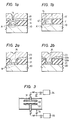
- Fig. la shows one example of such proposal, in which a wiring of a dual layer construction comprising a first wiring layer 12 and a second wiring layer 13 is shown (C.Y. Tiry, J. Vac. Sci. Technol., 21 (1) 1982, P14 - P18).
- the first wiring layer 12 of transition metal or compounds thereof such as TiN, TiW,.W,"Mo is provided to prevent occurrence of reaction between the second wiring layer 13 formed of alloy containing Al as a main component and a substrate 10 within a contact hole 14.
- the wiring layer 12 is extremely thin in a bottom end portion A of the contact hole 14 formed in an insulating film 11.
- the degree of such thinness is affected by the aspect ratio of the contact hole 14, method of forming the first wiring layer 12 and film thickness thereof.
- the aspect ratio of the contact hole is 1
- the step coverage factor (the ratio of film thickness) between a thick portion of a wiring layer and a thin portion thereof in the contact hole) is 0.1 to 0.5.
- the thickness of the first wiring layer 12 is reduced as described above, the effect of preventing the reaction between the second wiring layer 13 and the substrate 10 is lowered and the reliability of wiring is lowered.
- the current capacity of the wiring (maximum current amount that may be applied to the wiring) is also lowered.
- a method has been proposed wherein a first wiring layer 12' is formed inside a contact hole 14 by selective chemical vapor deposition (hereinafter referred to as "selective CVD"), as shown in Fig. lb, (C.E. Miller, Solid State Technol., Dec. 1982, 85).
- the first wiring layer 12' of transition metal such as W, Mo, etc. is selectively formed within the contact hole, and the contact hole 14 is embedded, after which a second wiring layer 13' is formed by sputtering or the like.
- the contact hole 14 is almost completely embedded or filled up by the first wiring layer 12', and therefore, the step coverage of the second wiring layer 13' and current capacity are improved over those shown in Fig. la.
- the present invention provides an arrangement wherein the thickness of a first wiring layer is made, on a side wall of a contact hole, gradually increasing from an upper portion toward a lower portion, to thereby effectively prevent a reaction between a second wiring layer and a substrate at the bottom end of the contact hole.
- a first wiring layer is provided to prevent a reaction between a semiconductor substrate at a bottom of a contact hole and a second wiring layer, and in the first wiring layer, a portion formed at the lower portion of the side wall of the contact hole is made greater in thickness than a portion formed on the upper portion of the side wall of the contact hole.
- an insulating film 21 having a contact hole 24, a first wiring layer 22 and a second wiring layer 23 are formed on a semiconductor substrate 20, and-the first wiring layer 22 within the contact hole 24 has a thickness thicker in a lower portion thereof than that in an upper portion thereof.
- the thickness of the first wiring layer 22 in the lower end portion B of the contact hole 24 is extremely qreat to effectively prevent a contact between the second wiring layer 23 and the semiconductor substrate 20 and reaction therebetween at the lower end portion B.
- the wiring layer in which,within the contact hole, the thickness of the lower portion is great whereas the thickness of the upper portion is small, can be formed by a method called "bias sputtering".
- normal sputtering comprises a method of bombarding high. speed ions (such as helium ions, neon ions etc.) against a source target formed of material forming a wiring,knocking out a material constituting the source target, accumulating the material locked out of the source target on the substrate arranged opposite of the source target, thus forming a film formed of said material on the substrate.
- high. speed ions such as helium ions, neon ions etc.
- the bias sputtering used in the present invention is characterized in that independent voltages are applied to both source target and substrate target on which a semiconductor substrate is placed, respectively, as shown in C.Y. Ting, et al., J. Vac. Sci. Technol. 15 (3), May/June 1978, P.1105 - P.1112. (This method is called “bias sputtering" because not . only a voltage is applied to a source target but also a bias voltage is applied to a substrate target.)
- Fig. 3 is a schematic view showing one example of such method.
- Independent power supplies (R.F. generators) 34, 35 are connected to an upper target (source target) 31 and a lower target (substrate target) 32, respectively, and a film formed of a material constituting the source target 31 is formed on a semiconductor substrate 33 placed on the substrate target 32.
- the present inventors have found that when a wiring layer is formed by the bias sputtering, the material is thickly accumulated on the lower portion of the side wall of the contact hole as shown in Fig. 2a. They have further found that the wiring layer formed by the bias sputtering is far more dense than the wiring formed by other methods such as normal sputtering or vacuum evaporation, and in addition, the adhesiveness with respect to the semiconductor and insulating film is far superior.
- At least the first wiring layer is formed by the bias sputtering whereby a wiring of extremely high reliability can be formed.
- the second wiring layer formed on the first wiring layer can be formed by various known methods such as normal sputtering, vacuum evaporation, etc.
- the bias sputtering is used, rugged portions on the upper surface are advantageously reduced.
- an insulating film 21 (Si0 2 ) having a thickness of 1 ⁇ m is formed on a silicon substrate 20 by a known heat oxidizing method, and a square contact hole 24 having a side length of 1 ⁇ m is formed by a known photoetching method.
- tungsten is accumulated in the contact hole 24 and on the insulating film 21 to form a first wiring layer 22 made of tungsten.
- the thickness in the lower end portion B of the contact hole 24 is more than 0.3 ⁇ m. This thickness of 0.3 ⁇ m is four to five times the thickness in the case a tungsten film is formed by normal sputtering..
- Al-Cu alloy (Cu 3%) having a thickness of 1 ⁇ m is formed under the same condition as before by the bias sputtering to form a second wiring layer 23.
- the thickness of the first wiring layer 22 in the lower end portion B of the contact hole 24 is extremely great, that is, four to five times that of prior art, and therefore, any reaction between the second wiring layer 23 and the silicon substrate 20 is completely prevented and the life time of the wiring is improved by more than twice over the case where formation of the first wiring layer having a thickness of 0.2 ⁇ m is performed by normal sputtering.
- the aforesaid resputtering rate is represented by a - b a, where a is the accumulated amount on the substrate when sputtering is carried out by not applying a voltage to the substrate electrode 32 but applying a voltage only to the source electrode 31, and b is the accumulated amount on the substrate when sputtering is carried out by applying a voltage to both substrate electrode 32 and source electrode 31.
- the resputtering rate can be adjusted to the desired value by varying the voltage (electric power) . applied to the substrate electrode 32 and/or source electrode 31. While Fig. 3 shows the case where R.F. power supplies 34, 35 are connected to substrate electrode 32 and source electrode 31, respectively,it should be noted that a DC power supply can be connected to the source electrode 31.
- An insulating film 21 having a contact hole 24 is formed in the same manner as in embodiment 1.
- a TiN film 22b is formed by the bias sputtering under the condition of a resputtering rate of 80%.
- the resputtering rate is so great as such, the surfaces of the substrate 20 and insulating film 21 are etched and fine particles caused by etching enter into the TiN film 22b and possibly deteriorate the purity of the TiN film 22b. Therefore, TiN film 22a having a thickness of 0.05 ⁇ m is formed by the normal sputtering in advance and then the TiN film 22b is formed thereon by the bias sputtering so as to form a first wiring layer having a thickness of 0.2 ⁇ m in total.
- a second wiring layer 23 of Al-Cu alloy is formed in the same manner as in embodiment 1.
- first wiring layers 22a, 22b can be formed of different material, for example, Ti can be used in place of TiN. In either case, it will suffice that the combined thickness of both layers is greater in the lower portion than in the upper portion within the contact hole.
- a silicon substrate is used in the above-described embodiment, but other semiconductor substrate, insulated substrate or metal substrate can be used.
- contact hole is used to connect a substrate with a wiring layer
- the contact hole is not limited to this purpose but can also be used to interconnect upper and lower wiring layers.
- various alloys principally containing Al or Cu such as Al-Si alloy, Al-Mn alloy and others can be used in addition to Al, Al-Cu alloy, etc.
- laminated films such as A1 ⁇ /X/Y/Al ⁇ Z can be used for the second wiring layer.
- X, Y, and Z can be noble metalsother than Al, transition metalsor alloys thereof, or nitride or silicate.
- X, Y and Z can be of the same kind of metal or different kinds of material.
- the first wiring layer there can be used at least one of various kinds of transition metals such as Ti, W, Mo, Pt, Pd, etc., alloys of those transition metals such as TiW, and various compounds of said transition metals such as titanium nitride, tungsten silicide, etc.
- transition metals such as Ti, W, Mo, Pt, Pd, etc.
- alloys of those transition metals such as TiW
- compounds of said transition metals such as titanium nitride, tungsten silicide, etc.
- the second wiring layer within the contact hole is preferably formed by the bias sputtering as described above, and a favorable result may be obtained if the resputtering rate is set to about 50 to 90%. If the resputtering rate is less than 50%, a cavity is sometimes formed in the filling layer. If the resputtering rate is above 90%, the accumulating speed of the film becomes extremely low.
- filling is not made only by the first wiring layer but is formed on the side surface and bottom surface, and therefore, a good result may be obtained by the bias sputtering at a resputtering above about 20%.
- the resputtering rate is less than about 20%, the thickness of the first wiring layer at the lower portion of the contact hole is sometimes insufficient, and therefore, it is preferable to set the resputtering rate above about 20%.
- a resputtering rate above 90% should be avoided since the accumulating speed is extremely low and the etching of the substrate and insulating film becomes conspicuous. Therefore, it is favorable to set the resputtering rate to about 20% to 90%.
Abstract
Description
- The present invention relates to a semiconductor device and method for manufacturing the same, and more particularly to a semiconductor device and method for manufacturing the same, which has a highly reliable wiring in a contact hole portion.
- With a trend of higher density of integration of a semiconductor integrated circuit, connecting portions of a wiring (such as a connecting portion between a wiring and a semiconductor substrate, a connecting portion between an upper layer wiring and a lower layer wiring, ect.) formed for connection between elements and the like are extremely reduced in dimension.
- The above-described connection is made through a contact hole formed in an insulating film, but the ratio of depth to diameter (or narrower width) of the contact hole (hereinafter referred to as "aspect ratio") also gradually increases.
- As a result, there occurs a tendency in that a defective connection is liable to occur to deteriorate the reliability of the wiring.
- A proposal has been made to provide a dual layer construction of a wiring in order to prevent the reliability from being deteriorated as described above.
- Fig. la shows one example of such proposal, in which a wiring of a dual layer construction comprising a
first wiring layer 12 and asecond wiring layer 13 is shown (C.Y. Tiry, J. Vac. Sci. Technol., 21 (1) 1982, P14 - P18). - The
first wiring layer 12 of transition metal or compounds thereof such as TiN, TiW,.W,"Mo is provided to prevent occurrence of reaction between thesecond wiring layer 13 formed of alloy containing Al as a main component and asubstrate 10 within acontact hole 14. - However, since the first and
second wiring layers wiring layer 12 is extremely thin in a bottom end portion A of thecontact hole 14 formed in aninsulating film 11. - The degree of such thinness is affected by the aspect ratio of the
contact hole 14, method of forming thefirst wiring layer 12 and film thickness thereof. For example, where the aspect ratio of the contact hole is 1, the step coverage factor (the ratio of film thickness) between a thick portion of a wiring layer and a thin portion thereof in the contact hole) is 0.1 to 0.5. - If in the end portion A, the thickness of the
first wiring layer 12 is reduced as described above, the effect of preventing the reaction between thesecond wiring layer 13 and thesubstrate 10 is lowered and the reliability of wiring is lowered. - Further, not only the thickness of the
first wiring layer 12 but also the thickness of thesecond wiring layer 13 become small in the end portion A for the same reason as described above, and therefore, the current capacity of the wiring (maximum current amount that may be applied to the wiring) is also lowered. - To solve the problem noted above, a method has been proposed wherein a first wiring layer 12' is formed inside a
contact hole 14 by selective chemical vapor deposition (hereinafter referred to as "selective CVD"), as shown in Fig. lb, (C.E. Miller, Solid State Technol., Dec. 1982, 85). - According to this method, the first wiring layer 12' of transition metal such as W, Mo, etc. is selectively formed within the contact hole, and the
contact hole 14 is embedded, after which a second wiring layer 13' is formed by sputtering or the like. - As clearly shown in Fig. lb, the contact hole 14 is almost completely embedded or filled up by the first wiring layer 12', and therefore, the step coverage of the second wiring layer 13' and current capacity are improved over those shown in Fig. la.
- However, as shown in Fig. lb, since the side of the first wiring layer 12' formed by the selective CVD and the side of the
insulating film 11 are not in close contact with each other but leave a gap therebetween, the thickness of the first wiring layer 12' becomes thin in the end portion A' similar to the case show in Fig. la, and the effect of preventing the reaction between the second wiring layer 13' and thesubstrate 10 is lowered, thus making it difficult to obtain a good wiring. Furthermore, three of the present inventors have proposed a method wherein a contact hole is filled with a first metal and thereafter a second metal layer is formed (see Japanese Patent Laid-Open No. 152192/82). However, it has been desired to develop a simpler and more practical method. - It is an object of the present invention to provide a semiconductor device and a method for manufacturing the same in which even if a dimension of a contact hole is made extremely small, a wiring having a high reliability is obtained, in overcoming those problems noted above with respect to prior art.
- To achieve the aforementioned object, the present invention provides an arrangement wherein the thickness of a first wiring layer is made, on a side wall of a contact hole, gradually increasing from an upper portion toward a lower portion, to thereby effectively prevent a reaction between a second wiring layer and a substrate at the bottom end of the contact hole.
-
- Figs. 1 and 2 are respectively views showing a sectional construction of a conventional wiring;
- Figs. 3 and 4 are respectively views showing a sectional construction of different embodiments of the present invention; and
- Fig. 3 is a schematic view for explaining bias sputtering used in the present invention.
- As described above, in the present invention, a first wiring layer is provided to prevent a reaction between a semiconductor substrate at a bottom of a contact hole and a second wiring layer, and in the first wiring layer, a portion formed at the lower portion of the side wall of the contact hole is made greater in thickness than a portion formed on the upper portion of the side wall of the contact hole.
- More specifically, as in one example shown in Fig. 2a, an
insulating film 21 having acontact hole 24, afirst wiring layer 22 and asecond wiring layer 23 are formed on asemiconductor substrate 20, and-thefirst wiring layer 22 within thecontact hole 24 has a thickness thicker in a lower portion thereof than that in an upper portion thereof. - Therefore, as is clear from Fig. 2a, the thickness of the
first wiring layer 22 in the lower end portion B of thecontact hole 24 is extremely qreat to effectively prevent a contact between thesecond wiring layer 23 and thesemiconductor substrate 20 and reaction therebetween at the lower end portion B. - The wiring layer in which,within the contact hole, the thickness of the lower portion is great whereas the thickness of the upper portion is small, can be formed by a method called "bias sputtering".
- As is known, normal sputtering comprises a method of bombarding high. speed ions (such as helium ions, neon ions etc.) against a source target formed of material forming a wiring,knocking out a material constituting the source target, accumulating the material locked out of the source target on the substrate arranged opposite of the source target, thus forming a film formed of said material on the substrate.
- The bias sputtering used in the present invention is characterized in that independent voltages are applied to both source target and substrate target on which a semiconductor substrate is placed, respectively, as shown in C.Y. Ting, et al., J. Vac. Sci. Technol. 15 (3), May/June 1978, P.1105 - P.1112. (This method is called "bias sputtering" because not . only a voltage is applied to a source target but also a bias voltage is applied to a substrate target.)
- Fig. 3 is a schematic view showing one example of such method. Independent power supplies (R.F. generators) 34, 35 are connected to an upper target (source target) 31 and a lower target (substrate target) 32, respectively, and a film formed of a material constituting the
source target 31 is formed on asemiconductor substrate 33 placed on thesubstrate target 32. - The present inventors have found that when a wiring layer is formed by the bias sputtering, the material is thickly accumulated on the lower portion of the side wall of the contact hole as shown in Fig. 2a. They have further found that the wiring layer formed by the bias sputtering is far more dense than the wiring formed by other methods such as normal sputtering or vacuum evaporation, and in addition, the adhesiveness with respect to the semiconductor and insulating film is far superior.
- The present invention has been achieved on the basis of the novel concept described above. At least the first wiring layer is formed by the bias sputtering whereby a wiring of extremely high reliability can be formed.
- Needless to say, the second wiring layer formed on the first wiring layer can be formed by various known methods such as normal sputtering, vacuum evaporation, etc. However, if the bias sputtering is used, rugged portions on the upper surface are advantageously reduced.
- As shown in Fig. 2a, an insulating film 21 (Si02) having a thickness of 1 µm is formed on a
silicon substrate 20 by a known heat oxidizing method, and asquare contact hole 24 having a side length of 1 µm is formed by a known photoetching method. - By the bias sputtering, tungsten is accumulated in the
contact hole 24 and on theinsulating film 21 to form afirst wiring layer 22 made of tungsten. - When the bias sputtering is carried out under the condition of a resputtering rate of 50% to form the
tungsten film 22 whose thickness in a flat portion is 0.2 µm, the thickness in the lower end portion B of thecontact hole 24 is more than 0.3 µm. This thickness of 0.3 µm is four to five times the thickness in the case
a tungsten film is formed by normal sputtering.. - Next, Al-Cu alloy (Cu 3%) having a thickness of 1 µm is formed under the same condition as before by the bias sputtering to form a
second wiring layer 23. - According to the above-described embodiment, the thickness of the
first wiring layer 22 in the lower end portion B of thecontact hole 24 is extremely great, that is, four to five times that of prior art, and therefore, any reaction between thesecond wiring layer 23 and thesilicon substrate 20 is completely prevented and the life time of the wiring is improved by more than twice over the case where formation of the first wiring layer having a thickness of 0.2 µm is performed by normal sputtering. - The aforesaid resputtering rate is represented by a - b a, where a is the accumulated amount on the substrate when sputtering is carried out by not applying a voltage to the
substrate electrode 32 but applying a voltage only to thesource electrode 31, and b is the accumulated amount on the substrate when sputtering is carried out by applying a voltage to bothsubstrate electrode 32 andsource electrode 31. - The resputtering rate can be adjusted to the desired value by varying the voltage (electric power) . applied to the
substrate electrode 32 and/orsource electrode 31. While Fig. 3 shows the case where R.F. power supplies 34, 35 are connected tosubstrate electrode 32 andsource electrode 31, respectively,it should be noted that a DC power supply can be connected to thesource electrode 31. - An insulating
film 21 having acontact hole 24 is formed in the same manner as in embodiment 1. - A
TiN film 22b is formed by the bias sputtering under the condition of a resputtering rate of 80%. However, where the resputtering rate is so great as such, the surfaces of thesubstrate 20 and insulatingfilm 21 are etched and fine particles caused by etching enter into theTiN film 22b and possibly deteriorate the purity of theTiN film 22b. Therefore,TiN film 22a having a thickness of 0.05 µm is formed by the normal sputtering in advance and then theTiN film 22b is formed thereon by the bias sputtering so as to form a first wiring layer having a thickness of 0.2 µm in total. - Thereafter, a
second wiring layer 23 of Al-Cu alloy is formed in the same manner as in embodiment 1. - It has been confirmed that as shown in Fig. 2b, the thus obtained wiring is great in thickness in the lower portion in the
contact hole 24 to effectively prevent reaction between thesecond wiring layer 23 andsubstrate 20, thus providing higher reliability and longer life time than in the prior art. - It will be noted that the
first wiring layers - It will be further noted that a silicon substrate is used in the above-described embodiment, but other semiconductor substrate, insulated substrate or metal substrate can be used.
- Moreover, while the case has been shown in which a contact hole is used to connect a substrate with a wiring layer, it will be noted than the contact hole is not limited to this purpose but can also be used to interconnect upper and lower wiring layers.
- Furthermore, while in the above-described embodiment, the case has been shown in which a first wiring layer is formed on the entire surface under a second wiring layer, it is possible that the first wiring layer is left only within the contact hole and is removed from the insulatinq film.
- For the second wiring layer, various alloys principally containing Al or Cu such as Al-Si alloy, Al-Mn alloy and others can be used in addition to Al, Al-Cu alloy, etc.
- Also, laminated films such as A1·/X/Y/Al·Z can be used for the second wiring layer. Here, X, Y, and Z can be noble metalsother than Al, transition metalsor alloys thereof, or nitride or silicate. Also, X, Y and Z can be of the same kind of metal or different kinds of material.
- For the first wiring layer, there can be used at least one of various kinds of transition metals such as Ti, W, Mo, Pt, Pd, etc., alloys of those transition metals such as TiW, and various compounds of said transition metals such as titanium nitride, tungsten silicide, etc.
- According to the present invention, the second wiring layer within the contact hole is preferably formed by the bias sputtering as described above, and a favorable result may be obtained if the resputtering rate is set to about 50 to 90%. If the resputtering rate is less than 50%, a cavity is sometimes formed in the filling layer. If the resputtering rate is above 90%, the accumulating speed of the film becomes extremely low.
- In the first wiring layer, filling is not made only by the first wiring layer but is formed on the side surface and bottom surface, and therefore, a good result may be obtained by the bias sputtering at a resputtering above about 20%.
- If the resputtering rate is less than about 20%, the thickness of the first wiring layer at the lower portion of the contact hole is sometimes insufficient, and therefore, it is preferable to set the resputtering rate above about 20%. A resputtering rate above 90% should be avoided since the accumulating speed is extremely low and the etching of the substrate and insulating film becomes conspicuous. Therefore, it is favorable to set the resputtering rate to about 20% to 90%.
Claims (11)
Applications Claiming Priority (2)
| Application Number | Priority Date | Filing Date | Title |
|---|---|---|---|
| JP147510/84 | 1984-07-18 | ||
| JP59147510A JPH069199B2 (en) | 1984-07-18 | 1984-07-18 | Wiring structure and manufacturing method thereof |
Publications (3)
| Publication Number | Publication Date |
|---|---|
| EP0168828A2 true EP0168828A2 (en) | 1986-01-22 |
| EP0168828A3 EP0168828A3 (en) | 1987-08-12 |
| EP0168828B1 EP0168828B1 (en) | 1992-01-15 |
Family
ID=15431982
Family Applications (1)
| Application Number | Title | Priority Date | Filing Date |
|---|---|---|---|
| EP85108953A Expired - Lifetime EP0168828B1 (en) | 1984-07-18 | 1985-07-17 | Method for manufacturing a semiconductor device having wiring layers |
Country Status (5)
| Country | Link |
|---|---|
| US (1) | US4792842A (en) |
| EP (1) | EP0168828B1 (en) |
| JP (1) | JPH069199B2 (en) |
| KR (1) | KR930007836B1 (en) |
| DE (1) | DE3585180D1 (en) |
Cited By (21)
| Publication number | Priority date | Publication date | Assignee | Title |
|---|---|---|---|---|
| EP0202572A2 (en) * | 1985-05-13 | 1986-11-26 | Nippon Telegraph And Telephone Corporation | Method for forming a planarized aluminium thin film |
| EP0300414A1 (en) * | 1987-07-20 | 1989-01-25 | Nippon Telegraph And Telephone Corporation | Method of connecting wirings through connection hole |
| US4884123A (en) * | 1987-02-19 | 1989-11-28 | Advanced Micro Devices, Inc. | Contact plug and interconnect employing a barrier lining and a backfilled conductor material |
| EP0351001A1 (en) * | 1988-07-12 | 1990-01-17 | Koninklijke Philips Electronics N.V. | Method for making a semi-conductor device with at least one level of interconnection with small dimensioned via holes |
| EP0376709A2 (en) * | 1988-12-29 | 1990-07-04 | Fujitsu Limited | Method of producing a semiconductor device by metal sputtering |
| US5356836A (en) * | 1993-08-19 | 1994-10-18 | Industrial Technology Research Institute | Aluminum plug process |
| US5374592A (en) * | 1992-09-22 | 1994-12-20 | Sgs-Thomson Microelectronics, Inc. | Method for forming an aluminum metal contact |
| US5397744A (en) * | 1991-02-19 | 1995-03-14 | Sony Corporation | Aluminum metallization method |
| US5472912A (en) * | 1989-11-30 | 1995-12-05 | Sgs-Thomson Microelectronics, Inc. | Method of making an integrated circuit structure by using a non-conductive plug |
| GB2296128A (en) * | 1993-09-15 | 1996-06-19 | Hyundai Electronics Ind | Formation of groves on conductors under via holes |
| US5591671A (en) * | 1994-01-18 | 1997-01-07 | Samsung Electronics Co., Ltd. | Method for interconnecting layers in semiconductor device |
| EP0766302A2 (en) * | 1995-09-27 | 1997-04-02 | Motorola, Inc. | Process for fabricating a CVD aluminium layer in a semiconductor device |
| US5658828A (en) * | 1989-11-30 | 1997-08-19 | Sgs-Thomson Microelectronics, Inc. | Method for forming an aluminum contact through an insulating layer |
| US5930673A (en) * | 1990-11-05 | 1999-07-27 | Stmicroelectronics, Inc. | Method for forming a metal contact |
| USRE36475E (en) * | 1993-09-15 | 1999-12-28 | Hyundai Electronics Industries Co., Ltd. | Method of forming a via plug in a semiconductor device |
| US6051490A (en) * | 1991-11-29 | 2000-04-18 | Sony Corporation | Method of forming wirings |
| USRE36663E (en) * | 1987-12-28 | 2000-04-18 | Texas Instruments Incorporated | Planarized selective tungsten metallization system |
| US6242811B1 (en) | 1989-11-30 | 2001-06-05 | Stmicroelectronics, Inc. | Interlevel contact including aluminum-refractory metal alloy formed during aluminum deposition at an elevated temperature |
| US6268290B1 (en) * | 1991-11-19 | 2001-07-31 | Sony Corporation | Method of forming wirings |
| US6271137B1 (en) | 1989-11-30 | 2001-08-07 | Stmicroelectronics, Inc. | Method of producing an aluminum stacked contact/via for multilayer |
| US6287963B1 (en) | 1990-11-05 | 2001-09-11 | Stmicroelectronics, Inc. | Method for forming a metal contact |
Families Citing this family (17)
| Publication number | Priority date | Publication date | Assignee | Title |
|---|---|---|---|---|
| US5175608A (en) * | 1987-06-30 | 1992-12-29 | Hitachi, Ltd. | Method of and apparatus for sputtering, and integrated circuit device |
| JPS6482547A (en) * | 1987-09-24 | 1989-03-28 | Tadahiro Omi | Semiconductor device |
| JPH0680736B2 (en) * | 1987-10-21 | 1994-10-12 | 工業技術院長 | Wiring formation method |
| US5132775A (en) * | 1987-12-11 | 1992-07-21 | Texas Instruments Incorporated | Methods for and products having self-aligned conductive pillars on interconnects |
| US5266835A (en) * | 1988-02-02 | 1993-11-30 | National Semiconductor Corporation | Semiconductor structure having a barrier layer disposed within openings of a dielectric layer |
| JP2537413B2 (en) * | 1989-03-14 | 1996-09-25 | 三菱電機株式会社 | Semiconductor device and manufacturing method thereof |
| US5730835A (en) * | 1996-01-31 | 1998-03-24 | Micron Technology, Inc. | Facet etch for improved step coverage of integrated circuit contacts |
| US6420786B1 (en) | 1996-02-02 | 2002-07-16 | Micron Technology, Inc. | Conductive spacer in a via |
| US6376781B1 (en) | 1996-05-03 | 2002-04-23 | Micron Technology, Inc. | Low resistance contacts fabricated in high aspect ratio openings by resputtering |
| US5929526A (en) * | 1997-06-05 | 1999-07-27 | Micron Technology, Inc. | Removal of metal cusp for improved contact fill |
| JP4947834B2 (en) * | 1997-11-26 | 2012-06-06 | アプライド マテリアルズ インコーポレイテッド | Damage-free coating engraving deposition method |
| US7253109B2 (en) | 1997-11-26 | 2007-08-07 | Applied Materials, Inc. | Method of depositing a tantalum nitride/tantalum diffusion barrier layer system |
| US6274486B1 (en) | 1998-09-02 | 2001-08-14 | Micron Technology, Inc. | Metal contact and process |
| US6423626B1 (en) | 1998-11-02 | 2002-07-23 | Micron Technology, Inc. | Removal of metal cusp for improved contact fill |
| US6261946B1 (en) * | 1999-01-05 | 2001-07-17 | Advanced Micro Devices, Inc. | Method for forming semiconductor seed layers by high bias deposition |
| US6537427B1 (en) | 1999-02-04 | 2003-03-25 | Micron Technology, Inc. | Deposition of smooth aluminum films |
| US9240378B2 (en) * | 2014-05-16 | 2016-01-19 | Taiwan Semiconductor Manufacturing Company Ltd. | Method of forming a copper layer using physical vapor deposition |
Citations (3)
| Publication number | Priority date | Publication date | Assignee | Title |
|---|---|---|---|---|
| JPS58108738A (en) * | 1981-12-22 | 1983-06-28 | Seiko Instr & Electronics Ltd | Manufacture of electrode for semiconductor device |
| FR2530383A1 (en) * | 1982-07-13 | 1984-01-20 | Thomson Csf | Monolithic integrated circuit comprising a Schottky logic section and a programmable memory with fuses |
| JPS60201655A (en) * | 1984-03-27 | 1985-10-12 | Seiko Epson Corp | Semiconductor device |
Family Cites Families (5)
| Publication number | Priority date | Publication date | Assignee | Title |
|---|---|---|---|---|
| JPS543480A (en) * | 1977-06-09 | 1979-01-11 | Fujitsu Ltd | Manufacture of semiconductor device |
| US4161430A (en) * | 1978-12-04 | 1979-07-17 | Burroughs Corporation | Method of forming integrated circuit metal interconnect structure employing molybdenum on aluminum |
| US4158613A (en) * | 1978-12-04 | 1979-06-19 | Burroughs Corporation | Method of forming a metal interconnect structure for integrated circuits |
| JPS592352A (en) * | 1982-06-28 | 1984-01-07 | Toshiba Corp | Manufacture of semiconductor device |
| JPH0620067B2 (en) * | 1982-10-08 | 1994-03-16 | 株式会社東芝 | Semiconductor device and manufacturing method thereof |
-
1984
- 1984-07-18 JP JP59147510A patent/JPH069199B2/en not_active Expired - Lifetime
-
1985
- 1985-07-12 KR KR1019850004971A patent/KR930007836B1/en not_active IP Right Cessation
- 1985-07-17 DE DE8585108953T patent/DE3585180D1/en not_active Expired - Lifetime
- 1985-07-17 EP EP85108953A patent/EP0168828B1/en not_active Expired - Lifetime
-
1987
- 1987-11-24 US US07/129,393 patent/US4792842A/en not_active Expired - Lifetime
Patent Citations (3)
| Publication number | Priority date | Publication date | Assignee | Title |
|---|---|---|---|---|
| JPS58108738A (en) * | 1981-12-22 | 1983-06-28 | Seiko Instr & Electronics Ltd | Manufacture of electrode for semiconductor device |
| FR2530383A1 (en) * | 1982-07-13 | 1984-01-20 | Thomson Csf | Monolithic integrated circuit comprising a Schottky logic section and a programmable memory with fuses |
| JPS60201655A (en) * | 1984-03-27 | 1985-10-12 | Seiko Epson Corp | Semiconductor device |
Non-Patent Citations (4)
| Title |
|---|
| EXTENDED ABSTRACTS, vol. 83, no. 2, 9th-14th October 1983, page 438, abstract no. 283, Washington, DC, US; Y. HOMMA et al.: "Planar deposition of aluminum by RF bias sputtering" * |
| JAPANESE JOURNAL OF APPLIED PHYSICS SUPPLEMENTS, 16th International Conference on Solid State Devices and Materials, 30th August - 1st September 1984, pages 43-46, Tokyo, JP; T. MOGAMI et al.: "Via-hole filling with molybdenum by RF Bias sputtering" * |
| PATENT ABSTRACTS OF JAPAN, vol. 10, no. 46 (E-383)[2103], 22nd February 1986; & JP-A-60 201 655 (SUWA SEIKOSHA K.K.) 12-10-1985 * |
| PATENT ABSTRACTS OF JAPAN, vol. 7, no. 214 (E-199)[1359], 21st September 1983, & JP-A-58 108 738 (DAINI SEIKOSHA K.K.) 28-06-1983 * |
Cited By (29)
| Publication number | Priority date | Publication date | Assignee | Title |
|---|---|---|---|---|
| EP0202572B1 (en) * | 1985-05-13 | 1993-12-15 | Nippon Telegraph And Telephone Corporation | Method for forming a planarized aluminium thin film |
| EP0202572A2 (en) * | 1985-05-13 | 1986-11-26 | Nippon Telegraph And Telephone Corporation | Method for forming a planarized aluminium thin film |
| US4884123A (en) * | 1987-02-19 | 1989-11-28 | Advanced Micro Devices, Inc. | Contact plug and interconnect employing a barrier lining and a backfilled conductor material |
| EP0300414A1 (en) * | 1987-07-20 | 1989-01-25 | Nippon Telegraph And Telephone Corporation | Method of connecting wirings through connection hole |
| USRE36663E (en) * | 1987-12-28 | 2000-04-18 | Texas Instruments Incorporated | Planarized selective tungsten metallization system |
| EP0351001A1 (en) * | 1988-07-12 | 1990-01-17 | Koninklijke Philips Electronics N.V. | Method for making a semi-conductor device with at least one level of interconnection with small dimensioned via holes |
| FR2634317A1 (en) * | 1988-07-12 | 1990-01-19 | Philips Nv | METHOD FOR MANUFACTURING SEMICONDUCTOR DEVICE HAVING AT LEAST ONE CONTACT LEVEL THROUGH SMALL DIMENSION CONTACT OPENINGS |
| EP0376709A3 (en) * | 1988-12-29 | 1990-10-10 | Fujitsu Limited | Method of producing a semiconductor device by metal sputtering |
| EP0376709A2 (en) * | 1988-12-29 | 1990-07-04 | Fujitsu Limited | Method of producing a semiconductor device by metal sputtering |
| US5976969A (en) * | 1989-11-30 | 1999-11-02 | Stmicroelectronics, Inc. | Method for forming an aluminum contact |
| US6271137B1 (en) | 1989-11-30 | 2001-08-07 | Stmicroelectronics, Inc. | Method of producing an aluminum stacked contact/via for multilayer |
| US5472912A (en) * | 1989-11-30 | 1995-12-05 | Sgs-Thomson Microelectronics, Inc. | Method of making an integrated circuit structure by using a non-conductive plug |
| US5658828A (en) * | 1989-11-30 | 1997-08-19 | Sgs-Thomson Microelectronics, Inc. | Method for forming an aluminum contact through an insulating layer |
| US6242811B1 (en) | 1989-11-30 | 2001-06-05 | Stmicroelectronics, Inc. | Interlevel contact including aluminum-refractory metal alloy formed during aluminum deposition at an elevated temperature |
| US6287963B1 (en) | 1990-11-05 | 2001-09-11 | Stmicroelectronics, Inc. | Method for forming a metal contact |
| US5930673A (en) * | 1990-11-05 | 1999-07-27 | Stmicroelectronics, Inc. | Method for forming a metal contact |
| US5397744A (en) * | 1991-02-19 | 1995-03-14 | Sony Corporation | Aluminum metallization method |
| US6268290B1 (en) * | 1991-11-19 | 2001-07-31 | Sony Corporation | Method of forming wirings |
| US6051490A (en) * | 1991-11-29 | 2000-04-18 | Sony Corporation | Method of forming wirings |
| US5374592A (en) * | 1992-09-22 | 1994-12-20 | Sgs-Thomson Microelectronics, Inc. | Method for forming an aluminum metal contact |
| US5356836A (en) * | 1993-08-19 | 1994-10-18 | Industrial Technology Research Institute | Aluminum plug process |
| GB2296128B (en) * | 1993-09-15 | 1998-09-23 | Hyundai Electronics Ind | Method of forming a via plug in a semiconductor device and a semiconductor device using its method |
| USRE36475E (en) * | 1993-09-15 | 1999-12-28 | Hyundai Electronics Industries Co., Ltd. | Method of forming a via plug in a semiconductor device |
| GB2296128A (en) * | 1993-09-15 | 1996-06-19 | Hyundai Electronics Ind | Formation of groves on conductors under via holes |
| USRE38383E1 (en) | 1993-09-15 | 2004-01-13 | Hyundai Electronics Industries Co. Ltd. | Method for forming a via plug in a semiconductor device |
| US6433435B2 (en) | 1993-11-30 | 2002-08-13 | Stmicroelectronics, Inc. | Aluminum contact structure for integrated circuits |
| US5591671A (en) * | 1994-01-18 | 1997-01-07 | Samsung Electronics Co., Ltd. | Method for interconnecting layers in semiconductor device |
| EP0766302A3 (en) * | 1995-09-27 | 1998-05-13 | Motorola, Inc. | Process for fabricating a CVD aluminium layer in a semiconductor device |
| EP0766302A2 (en) * | 1995-09-27 | 1997-04-02 | Motorola, Inc. | Process for fabricating a CVD aluminium layer in a semiconductor device |
Also Published As
| Publication number | Publication date |
|---|---|
| EP0168828B1 (en) | 1992-01-15 |
| KR930007836B1 (en) | 1993-08-20 |
| EP0168828A3 (en) | 1987-08-12 |
| JPS6127657A (en) | 1986-02-07 |
| JPH069199B2 (en) | 1994-02-02 |
| KR860001495A (en) | 1986-02-26 |
| US4792842A (en) | 1988-12-20 |
| DE3585180D1 (en) | 1992-02-27 |
Similar Documents
| Publication | Publication Date | Title |
|---|---|---|
| EP0168828B1 (en) | Method for manufacturing a semiconductor device having wiring layers | |
| US5266526A (en) | Method of forming trench buried wiring for semiconductor device | |
| US4924295A (en) | Integrated semi-conductor circuit comprising at least two metallization levels composed of aluminum or aluminum compounds and a method for the manufacture of same | |
| US5691572A (en) | Interconnect structures for integrated circuits | |
| JP3330495B2 (en) | Thin metal barrier layer for electrical interconnection | |
| US4898841A (en) | Method of filling contact holes for semiconductor devices and contact structures made by that method | |
| US6566258B1 (en) | Bi-layer etch stop for inter-level via | |
| JPH08204005A (en) | Semiconductor device and its manufacturing method | |
| JPH0680737B2 (en) | Method for manufacturing semiconductor device | |
| US5972786A (en) | Contact hole structure in a semiconductor and formation method therefor | |
| EP0455341B1 (en) | Semiconductor contact via structure and method | |
| US6614114B2 (en) | Conductive line formed on integrated circuits | |
| US6218287B1 (en) | Method of fabricating a semiconductor structure | |
| US4456506A (en) | Superconducting circuit fabrication | |
| EP1121717A1 (en) | Improved methods for barrier layer formation | |
| JPH0228253B2 (en) | ||
| JP2000091266A (en) | Method for improvement of aluminum metallized structure for tungsten etch back process | |
| US6274476B1 (en) | Semiconductor device and method of manufacturing the same | |
| US6417568B1 (en) | Semiconductor device | |
| US20010010401A1 (en) | Semiconductor device having a wiring layer of copper | |
| JP7343407B2 (en) | Metal wiring formation method and metal wiring structure | |
| JP3337758B2 (en) | Method for manufacturing semiconductor device | |
| JP2546482B2 (en) | Semiconductor device and manufacturing method thereof | |
| JPH0786209A (en) | Manufacture of semiconductor device | |
| JP2891195B2 (en) | Method for manufacturing semiconductor device |
Legal Events
| Date | Code | Title | Description |
|---|---|---|---|
| PUAI | Public reference made under article 153(3) epc to a published international application that has entered the european phase |
Free format text: ORIGINAL CODE: 0009012 |
|
| AK | Designated contracting states |
Designated state(s): DE FR GB IT |
|
| PUAL | Search report despatched |
Free format text: ORIGINAL CODE: 0009013 |
|
| AK | Designated contracting states |
Kind code of ref document: A3 Designated state(s): DE FR GB IT |
|
| 17P | Request for examination filed |
Effective date: 19871223 |
|
| 17Q | First examination report despatched |
Effective date: 19900227 |
|
| GRAA | (expected) grant |
Free format text: ORIGINAL CODE: 0009210 |
|
| AK | Designated contracting states |
Kind code of ref document: B1 Designated state(s): DE FR GB IT |
|
| PG25 | Lapsed in a contracting state [announced via postgrant information from national office to epo] |
Ref country code: IT Free format text: LAPSE BECAUSE OF FAILURE TO SUBMIT A TRANSLATION OF THE DESCRIPTION OR TO PAY THE FEE WITHIN THE PRESCRIBED TIME-LIMIT;WARNING: LAPSES OF ITALIAN PATENTS WITH EFFECTIVE DATE BEFORE 2007 MAY HAVE OCCURRED AT ANY TIME BEFORE 2007. THE CORRECT EFFECTIVE DATE MAY BE DIFFERENT FROM THE ONE RECORDED. Effective date: 19920115 Ref country code: FR Effective date: 19920115 |
|
| REF | Corresponds to: |
Ref document number: 3585180 Country of ref document: DE Date of ref document: 19920227 |
|
| EN | Fr: translation not filed | ||
| PLBE | No opposition filed within time limit |
Free format text: ORIGINAL CODE: 0009261 |
|
| STAA | Information on the status of an ep patent application or granted ep patent |
Free format text: STATUS: NO OPPOSITION FILED WITHIN TIME LIMIT |
|
| 26N | No opposition filed | ||
| PGFP | Annual fee paid to national office [announced via postgrant information from national office to epo] |
Ref country code: GB Payment date: 19990625 Year of fee payment: 15 |
|
| PG25 | Lapsed in a contracting state [announced via postgrant information from national office to epo] |
Ref country code: GB Free format text: LAPSE BECAUSE OF NON-PAYMENT OF DUE FEES Effective date: 20000717 |
|
| PGFP | Annual fee paid to national office [announced via postgrant information from national office to epo] |
Ref country code: DE Payment date: 20000928 Year of fee payment: 16 |
|
| GBPC | Gb: european patent ceased through non-payment of renewal fee |
Effective date: 20000717 |
|
| PG25 | Lapsed in a contracting state [announced via postgrant information from national office to epo] |
Ref country code: DE Free format text: LAPSE BECAUSE OF NON-PAYMENT OF DUE FEES Effective date: 20020501 |