EP0174476A2 - Photographic camera with electronic image enhancement - Google Patents
Photographic camera with electronic image enhancement Download PDFInfo
- Publication number
- EP0174476A2 EP0174476A2 EP85109360A EP85109360A EP0174476A2 EP 0174476 A2 EP0174476 A2 EP 0174476A2 EP 85109360 A EP85109360 A EP 85109360A EP 85109360 A EP85109360 A EP 85109360A EP 0174476 A2 EP0174476 A2 EP 0174476A2
- Authority
- EP
- European Patent Office
- Prior art keywords
- photosensitive material
- scene
- light
- photographic camera
- electrical signal
- Prior art date
- Legal status (The legal status is an assumption and is not a legal conclusion. Google has not performed a legal analysis and makes no representation as to the accuracy of the status listed.)
- Granted
Links
Images


Classifications
-
- G—PHYSICS
- G03—PHOTOGRAPHY; CINEMATOGRAPHY; ANALOGOUS TECHNIQUES USING WAVES OTHER THAN OPTICAL WAVES; ELECTROGRAPHY; HOLOGRAPHY
- G03B—APPARATUS OR ARRANGEMENTS FOR TAKING PHOTOGRAPHS OR FOR PROJECTING OR VIEWING THEM; APPARATUS OR ARRANGEMENTS EMPLOYING ANALOGOUS TECHNIQUES USING WAVES OTHER THAN OPTICAL WAVES; ACCESSORIES THEREFOR
- G03B7/00—Control of exposure by setting shutters, diaphragms or filters, separately or conjointly
- G03B7/28—Circuitry to measure or to take account of the object contrast
Definitions
- This invention relates generally to a photographic camera apparatus with electronic image enhancement and, more particularly, to a photographic camera apparatus in which a photosensitive material is both optically exposed to image scene light and electronically exposed to electronically sensed image scene light.
- Photographic cameras which operate to optically expose a photosensitive material to image scene light are very well established in the art. Such cameras may embody elaborate exposure control systems for precisely controlling the time of exposure as well as the size of the exposing aperture in accordance with the intensity of the light detected from the scene to be photographed.
- exposure control systems for precisely controlling the time of exposure as well as the size of the exposing aperture in accordance with the intensity of the light detected from the scene to be photographed.
- Electronic imaging cameras such as that disclosed by U.S. Patent No. 4,384,336 operate to detect image data electronically and manipulate electronic signal information so as to compensate for such unfavorable or difficult scene lighting conditions to provide satisfactory hard copy prints.
- Such electronic imaging cameras in some respects represent a substantial advance in the art because of their ability to provide some degree of image enhancement or compensation. However, such cameras may not achieve the high degree of image resolution provided by conventional photographic camera apparatus.
- the invention accordingly comprises a mechanism and system possessing the construction, combination of elements and arrangement of parts which are exemplified in the following detailed disclosure.
- a photographic camera apparatus providing for electronic image enhancement comprises means for controlling the exposure of a photosensitive material to scene light received directly from a scene in such a manner that the photosensitive material is exposed to a lesser extent than would be required for a selected optimum exposure value.
- Means is also provided for sensing the scene light from the photographic scene during the exposure and for converting the sensed scene light to electrical signal information corresponding to the sensed scene light.
- Means responding to the electrical signal information then expose the photosensitive material to an extent which in conjunction with the direct exposure to scene light substantially provides the selected optimum exposure value.
- the scene light sensing means preferably senses the scene light at a resolution substantially less than the resolution at which the photosensitive material is exposed during its direct exposure to scene light.
- the exposing means responds to the electrical signal information and generally comprises means for processing and thereby altering the electrical signal information so as to ultimately enhance the recorded image of the scene.
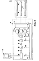
- FIG. 1 there is shown a photographic camera apparatus 10 embodying the present invention.
- the camera 10 includes an electronic flash unit 12 preferably of the quench type and mounted on a rigid body 14 for movement between an erect operative position as shown and a folded inoperative position (not illustrated).
- the camera body 14 includes a generally prismatic shaped major housing 16, a generally L-shaped front housing 18, and a generally rectangularly shaped film loading door 20 which together define the outward appearance of the camera 10 and which house and protect its interior components.
- the film loading door 20 includes an elongated film exit slot 46.
- the housings 16 and 18 and the film loading door 20 are all preferably molded of an opaque plastic to preclude unwanted light from entering the camera interior.
- the flash unit 12 includes a source of illumination having an output window 22 arranged so that the light output from the flash is directed toward the scene.
- a source of illumination having an output window 22 arranged so that the light output from the flash is directed toward the scene.
- a film cassette receiving chamber 24 Formed in the base of the prismatic housing 16 is a film cassette receiving chamber 24.
- the chamber 24 is adapted to releasably hold a film cassette 26.
- the film cassette 26 comprises a generally rectangular parallelepiped housing 28 which has an upwardly facing wall 30 framing a generally rectangular aperture 32.
- Mounted in registration with and biased towards the aperture 32 is a stack of integral type self-processable film units the top one of which is shown at 34.
- Each of the film units has a film speed requiring a predetermined exposure which is provided by the camera in the manner of this invention.
- Underneath the stack of film units is a flat thin battery (not shown) which is electrically coupled to power various electrical systems of the camera apparatus 10. Examples of the film cassette are described in U.S. Patents No. 3,872,487, 3,415,644, 3,594,165 and 3,761,268.
- the housing 16 In front of the housing 16 there is provided an objective lens 36 through which the optical axis O A of the camera extends.
- the housing 16 encloses an exposure chamber 38 within which a trapezoidally shaped mirror 40 is arranged at a predetermined angle with respect to the optical axis O A and the film plane to provide a folded light path of predetermined length between the objective lens 36 and the top film unit 34 in the film cassette 26.
- the exposure chamber 38 may be of the type which is described in U.S. Patent No. 4,057,815.
- the housing 16 further includes a negative lens 42 as part of a reversed Galilean viewfinder structured to have a field of view substantially coextensive with that of the objective lens to enable the user to frame and compose the subject matter to be photographed.
- a negative lens 42 as part of a reversed Galilean viewfinder structured to have a field of view substantially coextensive with that of the objective lens to enable the user to frame and compose the subject matter to be photographed.
- Individual film units 34 after being exposed to scene light by way of the objective taking lens 36 and trapezoidal mirror 40 in the manner of this invention, are advanced from the camera through a pair of film processing rollers 48 and the elongated film exit slot 46.
- the photographic camera apparatus 10 additionally includes a low resolution photoresponsive detector 50 which preferably comprises 128 x 128 Charge Coupled Device (CCD) array 51 (see FIG. 2) with colored filter stripes or patches disposed on it so that red, green and blue intensities can be detected for each low resolution pixel element.
- the preferred pattern for the filter stripes is repeating red, green, blue and green stripes.
- Scene light is directed to the CCD array 51 by way of an objective lens 53 and a conventional shutter (not shown).
- the output from the photoresponsive detector 50 is directed to an electronic image processor 52 which operates to process or enhance the electronic signal information derived from the photoresponsive detector 50.
- the electronic image processor 52 provides output signals to three linear arrays of color light exposing elements 54, 56 and 58.
- the linear arrays of color light exposing elements 54, 56, 58 preferably comprise, respectively, a row of 128 blue Light Emitting Diodes (LED's), a row of 128 green LED's and a row of 128 red LED's.
- LED's
- FIG. 2 there is schematically shown the circuit of the electronic image processor 52.
- the electronic signal data from the CCD array 51 is clocked to a shift register 60 by a timing and control circuit clock 82.
- the output signal of the shift register 60 is directed to a preamplifier 62 and is then sampled and held in a sample and hold circuit 64.
- the signal is thereafter directed into an amplifier 66 and thereafter is converted from an analog signal to a digital signal by an A/D converter 68.
- the digital signal is clocked into successive locations in a random access memory (RAM) 70.
- RAM random access memory
- the digitized data from the RAM 70 thereafter is directed by way of three latches 72, 74 and 76 to a programmable read only memory (PROM) 78 from which the data is directed to the linear arrays of color light exposing elements 54, 56 and 58.
- PROM programmable read only memory
- Operation of the photographic camera apparatus of this invention proceeds in the following manner.
- the photographer commences a photographic exposure cycle in the usual manner by actuating a photographic cycle initiation button (not shown) on the camera 10 after framing and composing the desired scene to be photographed.
- Scene light is thereafter directed by the objective taking lens 36 along the optical axis O A through a shutter system (not shown) to the trapezoidally shaped mirror 40 whence it is reflected to expose an integral self-processable film unit 34.
- This aspect of the photographic exposure is conventional with the exception that the film unit 34 is exposed to an extent less than required for its optimum exposure value. Thus, the film unit 34 is deliberately underexposed.
- the photoresponsive detector 50 electronically measures the scene light in low resolution for a selected exposure interval as determined by its shutter (not shown).
- the timing and control circuit clock 82 thereafter operates to clock the electronic image data for every color of the CCD array 51 into the shift register 60 whereafter for each horizontal line clocked into the shift register 60, the shift register clocks out each pixel.
- the charge packets from the shift register 60 are thereafter directed to the preamplifier 62 whence they are sampled and held by the sample and hold circuit 64.
- the sampled signal is thereafter directed into the amplifier 66 and converted into a digital signal format by the analog to digital (A/D) converter 68.
- Each analog signal value for each pixel is preferably converted into a four bit digital signal value.
- the digital values are thereafter clocked by the timing and control circuit clock 82 into successive locations in the random access memory (RAM) 70.
- the signal content of the CCD array 51 is digitized and stored in a random access memory (RAM) 70.
- the random access memory (RAM) 70 is required to hold four bits times 128 times 128 pixels equal to 65,536 bits of information.
- the digitized electronic signal data stored in the RAM 70 is thereafter clocked out and used to control an electronic second exposure in the manner of this invention.
- the digitized pixel image values for each horizontal line are stored in the RAM 70 in the pattern of the filter stripes: red, green, blue, green, etc. and are thereafter converted to three parallel lines of red, green and blue pixel signal data by replicating the measured image pixel data to estimate red, green and blue image signal values for every pixel of the CCD array in the following manner.
- the digitized image data is clocked out of the RAM 70 by the timing and control circuit clock 82 to the three different latches 72, 74 and 76 corresponding, respectively, to the red, green and blue image data.
- the red pixel latch 72 is clocked once for every fourth system clock pulse
- the green pixel latch 74 is clocked once for every other system clock pulse
- the blue latch 76 is clocked once for every fourth system clock pulse.
- Each of the three latches 72, 74 and 76 holds its four bit digitized pixel value until the next succeeding clock pulse from the timing and control circuit clock 82 appears. In this manner, each latch holds the value of the most recent pixel occurring for that color in the currently processed line providing a simultaneous estimate of R, G and B for each pixel.
- the digital pixel signal values are directed from the latch circuits 72, 74 and 76 into the programmable read only memory (PROM) which may include a look-up table containing the desired image processing information.
- PROM programmable read only memory
- the red, green and blue output signal values from the PROM 78 are directed respectively to the red, green and blue linear arrays of color light exposing elements 58, 56 and 54 to additionally expose the previously exposed top film unit 34 as it is advanced from the photographic camera 10 in the usual manner by the juxtaposed film processing rollers 48.
- the undesired film characteristics or unfavorable scene lighting conditions may be compensated or the desired image processing effect may be provided through this additional exposure.
- colors may be made more saturated by adding more red exposure where the detector 50 measured red pixel data.
- the programmable read only memory (PROM) 78 would receive 12 bits of digitized signal data for each pixel element sensed by the CCD array 51 and, in turn, provide 12 output bits of digitized signal data to drive corresponding light emitting diodes in the linear arrays 54, 56 and 58.
- Such digitized data may be utilized to drive the linear arrays in any manner, for instance, as disclosed by British Patent Specification No. 2,104,266.
- the electronic image processor 52 in conjunction with the photoresponsive detector 50 provides a means for sensing the light from the scene to be photographed during the actual photographic exposure so as to convert the sensed scene light to electrical signal information corresponding to the sensed scene light.
- the linear arrays of color light exposing elements 54, 56 and 58 provide a means responsive to the electrical signal information to expose the photosensitive material to an extent which in conjunction with the direct exposure to scene light substantially provides a select optimum exposure value.
- the PROM 78 may apply an exposure transform to the inputted R,G,B signal values in accordance with the following matrix wherein R, G, and B represent the red, green and blue digitized signal values input to the PROM 78 from the latches 72, 74 and 76, respectively, wherein R', G' and B' represent the corresponding red, green and blue transform digitized signal values output from the PROM 78 and wherein 6 may typically be in the order of 0.25.
- the aforementioned matrix may be derived from a matrix transformation by subtracting therefrom the exposure values provided optically by the photographic exposure through the objective lens as follows.
- the exposure values provided optically are shown by way of example to be 1 although as is readily apparent such exposure values could also be less than 1.
- FIGS. 3 and 4 there is shown an alternate arrangement which replaces the linear arrays of color light exposing elements with red, green and blue lights shown respectively at 82, 84 and 86.
- the red, green and blue lights 82, 84 and 86 are each respectively optically connected to an appropriate light dispersing optical element 88 to provide a substantially uniform light throughout the exposure chamber 38.
- a liquid crystal array 90 is provided in overlying relationship with respect to the top film unit 34 so as to control the added exposure in the aforementioned manner.
- FIG. 3 shows the addition of three buffer circuits 92, 94 and 96 to the red, green and blue output terminals respectively from the PROM 78 to enable the memory read-out process to occur consecutively starting with all the red pixel signal data modulating the LCD 90 while the red light 82 is turned on and thereafter switching to transfer all the green pixel signal data to the LCD 90 while the green light 84 is turned on and thereafter finally transferring all the blue pixel signal data to the LCD 90 while the blue light is turned on.
- any other means responsive to the electrical signal information may be utilized for exposing the photosensitive material to an extent which in conjunction with the direct optical exposure to scene light substantially provides the selected optimum exposure value.
- a camera apparatus utilizing instant developing film has been shown and described, the scope of invention is by no means so limited and extends to camera systems utilizing conventional type film.
Abstract
Description
- This invention relates generally to a photographic camera apparatus with electronic image enhancement and, more particularly, to a photographic camera apparatus in which a photosensitive material is both optically exposed to image scene light and electronically exposed to electronically sensed image scene light.
- Photographic cameras which operate to optically expose a photosensitive material to image scene light are very well established in the art. Such cameras may embody elaborate exposure control systems for precisely controlling the time of exposure as well as the size of the exposing aperture in accordance with the intensity of the light detected from the scene to be photographed. However, despite advances in the state of the art made with respect to exposure control systems, there still exist situations in which unfavorable or difficult scene lighting conditions as well as limitations in film sensitivity characteristics may contribute to a less than favorable exposure.
- Electronic imaging cameras such as that disclosed by U.S. Patent No. 4,384,336 operate to detect image data electronically and manipulate electronic signal information so as to compensate for such unfavorable or difficult scene lighting conditions to provide satisfactory hard copy prints. Such electronic imaging cameras in some respects represent a substantial advance in the art because of their ability to provide some degree of image enhancement or compensation. However, such cameras may not achieve the high degree of image resolution provided by conventional photographic camera apparatus.
- Therefore, it is a primary object of this invention to provide a photographic camera apparatus capable of yielding high resolution quality photographic prints electronically enhanced to compensate for both difficult or unfavorable scene lighting conditions and limitations in the film characteristics.
- Other objects of the invention will in part be obvious and will in part appear hereinafter. The invention accordingly comprises a mechanism and system possessing the construction, combination of elements and arrangement of parts which are exemplified in the following detailed disclosure.
- A photographic camera apparatus providing for electronic image enhancement comprises means for controlling the exposure of a photosensitive material to scene light received directly from a scene in such a manner that the photosensitive material is exposed to a lesser extent than would be required for a selected optimum exposure value. Means is also provided for sensing the scene light from the photographic scene during the exposure and for converting the sensed scene light to electrical signal information corresponding to the sensed scene light. Means responding to the electrical signal information then expose the photosensitive material to an extent which in conjunction with the direct exposure to scene light substantially provides the selected optimum exposure value. The scene light sensing means preferably senses the scene light at a resolution substantially less than the resolution at which the photosensitive material is exposed during its direct exposure to scene light. The exposing means responds to the electrical signal information and generally comprises means for processing and thereby altering the electrical signal information so as to ultimately enhance the recorded image of the scene.
- The novel features that are considered characteristic of the invention are set forth with particularity in the appended claims. The invention itself, however, both as to its organization and its method of operation, together with other objects and advantages thereof will be best understood from the following description of the illustrated embodiment when read in connection with the accompanying drawings wherein:
- FIG. 1 is a perspective view partly in phantom of a photographic camera apparatus embodying the electronic image enhancing feature of this invention;
- FIG. 2 is an electronic circuit diagram of the electronic image enhancing feature of this invention;
- FIG. 3 is a schematic diagram for an alternate embodiment showing a portion of the electronic image enhancing feature of this invention; and
- FIG. 4 is a perspective view partly in phantom of an alternate embodiment for a photographic camera apparatus embodying the electronic image enhancing feature of this invention.
- In FIG. 1 there is shown a photographic camera apparatus 10 embodying the present invention. The camera 10 includes an
electronic flash unit 12 preferably of the quench type and mounted on arigid body 14 for movement between an erect operative position as shown and a folded inoperative position (not illustrated). Thecamera body 14 includes a generally prismatic shapedmajor housing 16, a generally L-shapedfront housing 18, and a generally rectangularly shapedfilm loading door 20 which together define the outward appearance of the camera 10 and which house and protect its interior components. Thefilm loading door 20 includes an elongatedfilm exit slot 46. Thehousings film loading door 20 are all preferably molded of an opaque plastic to preclude unwanted light from entering the camera interior. - The
flash unit 12 includes a source of illumination having anoutput window 22 arranged so that the light output from the flash is directed toward the scene. For a more detailed description of the flash unit folding arrangement, see U.S. Patent No. 4,268,146. - Formed in the base of the
prismatic housing 16 is a filmcassette receiving chamber 24. Thechamber 24 is adapted to releasably hold afilm cassette 26. Thefilm cassette 26 comprises a generally rectangularparallelepiped housing 28 which has an upwardly facingwall 30 framing a generallyrectangular aperture 32. Mounted in registration with and biased towards theaperture 32 is a stack of integral type self-processable film units the top one of which is shown at 34. Each of the film units has a film speed requiring a predetermined exposure which is provided by the camera in the manner of this invention. Underneath the stack of film units is a flat thin battery (not shown) which is electrically coupled to power various electrical systems of the camera apparatus 10. Examples of the film cassette are described in U.S. Patents No. 3,872,487, 3,415,644, 3,594,165 and 3,761,268. - In front of the
housing 16 there is provided anobjective lens 36 through which the optical axis OA of the camera extends. Thehousing 16 encloses anexposure chamber 38 within which a trapezoidallyshaped mirror 40 is arranged at a predetermined angle with respect to the optical axis OA and the film plane to provide a folded light path of predetermined length between theobjective lens 36 and thetop film unit 34 in thefilm cassette 26. Theexposure chamber 38 may be of the type which is described in U.S. Patent No. 4,057,815. - In its front face the
housing 16 further includes anegative lens 42 as part of a reversed Galilean viewfinder structured to have a field of view substantially coextensive with that of the objective lens to enable the user to frame and compose the subject matter to be photographed. -
Individual film units 34, after being exposed to scene light by way of theobjective taking lens 36 andtrapezoidal mirror 40 in the manner of this invention, are advanced from the camera through a pair offilm processing rollers 48 and the elongatedfilm exit slot 46. - The photographic camera apparatus 10 additionally includes a low resolution
photoresponsive detector 50 which preferably comprises 128 x 128 Charge Coupled Device (CCD) array 51 (see FIG. 2) with colored filter stripes or patches disposed on it so that red, green and blue intensities can be detected for each low resolution pixel element. The preferred pattern for the filter stripes is repeating red, green, blue and green stripes. Scene light is directed to theCCD array 51 by way of anobjective lens 53 and a conventional shutter (not shown). The output from thephotoresponsive detector 50 is directed to anelectronic image processor 52 which operates to process or enhance the electronic signal information derived from thephotoresponsive detector 50. Theelectronic image processor 52, in turn, provides output signals to three linear arrays of colorlight exposing elements light exposing elements - Referring now to FIG. 2, there is schematically shown the circuit of the
electronic image processor 52. The electronic signal data from theCCD array 51 is clocked to ashift register 60 by a timing andcontrol circuit clock 82. The output signal of theshift register 60 is directed to apreamplifier 62 and is then sampled and held in a sample and holdcircuit 64. The signal is thereafter directed into anamplifier 66 and thereafter is converted from an analog signal to a digital signal by an A/D converter 68. The digital signal is clocked into successive locations in a random access memory (RAM) 70. The digitized data from theRAM 70 thereafter is directed by way of threelatches light exposing elements - Operation of the photographic camera apparatus of this invention proceeds in the following manner. The photographer commences a photographic exposure cycle in the usual manner by actuating a photographic cycle initiation button (not shown) on the camera 10 after framing and composing the desired scene to be photographed. Scene light is thereafter directed by the
objective taking lens 36 along the optical axis OA through a shutter system (not shown) to the trapezoidallyshaped mirror 40 whence it is reflected to expose an integral self-processable film unit 34. This aspect of the photographic exposure is conventional with the exception that thefilm unit 34 is exposed to an extent less than required for its optimum exposure value. Thus, thefilm unit 34 is deliberately underexposed. - Simultaneously with the aforementioned photographic exposure, the
photoresponsive detector 50 electronically measures the scene light in low resolution for a selected exposure interval as determined by its shutter (not shown). The timing and controlcircuit clock 82 thereafter operates to clock the electronic image data for every color of theCCD array 51 into theshift register 60 whereafter for each horizontal line clocked into theshift register 60, the shift register clocks out each pixel. The charge packets from theshift register 60 are thereafter directed to thepreamplifier 62 whence they are sampled and held by the sample and holdcircuit 64. The sampled signal is thereafter directed into theamplifier 66 and converted into a digital signal format by the analog to digital (A/D)converter 68. Each analog signal value for each pixel is preferably converted into a four bit digital signal value. The digital values are thereafter clocked by the timing and controlcircuit clock 82 into successive locations in the random access memory (RAM) 70. In this manner the signal content of theCCD array 51 is digitized and stored in a random access memory (RAM) 70. As is readily apparent, since thephotoresponsive detector 50 has a 128 x 128 pixel resolution, the random access memory (RAM) 70 is required to hold four bits times 128 times 128 pixels equal to 65,536 bits of information. - The digitized electronic signal data stored in the
RAM 70 is thereafter clocked out and used to control an electronic second exposure in the manner of this invention. The digitized pixel image values for each horizontal line are stored in theRAM 70 in the pattern of the filter stripes: red, green, blue, green, etc. and are thereafter converted to three parallel lines of red, green and blue pixel signal data by replicating the measured image pixel data to estimate red, green and blue image signal values for every pixel of the CCD array in the following manner. The digitized image data is clocked out of theRAM 70 by the timing and controlcircuit clock 82 to the threedifferent latches CCD array 51 is in the ordered sequence of red, green, blue, green stripes, it is readily apparent that thered pixel latch 72 is clocked once for every fourth system clock pulse, thegreen pixel latch 74 is clocked once for every other system clock pulse and theblue latch 76 is clocked once for every fourth system clock pulse. Each of the three latches 72, 74 and 76 holds its four bit digitized pixel value until the next succeeding clock pulse from the timing and controlcircuit clock 82 appears. In this manner, each latch holds the value of the most recent pixel occurring for that color in the currently processed line providing a simultaneous estimate of R, G and B for each pixel. - The digital pixel signal values are directed from the
latch circuits PROM 78 are directed respectively to the red, green and blue linear arrays of colorlight exposing elements top film unit 34 as it is advanced from the photographic camera 10 in the usual manner by the juxtaposedfilm processing rollers 48. - Thus, the undesired film characteristics or unfavorable scene lighting conditions may be compensated or the desired image processing effect may be provided through this additional exposure. For example, colors may be made more saturated by adding more red exposure where the
detector 50 measured red pixel data. In this example the programmable read only memory (PROM) 78 would receive 12 bits of digitized signal data for each pixel element sensed by theCCD array 51 and, in turn, provide 12 output bits of digitized signal data to drive corresponding light emitting diodes in thelinear arrays - In this manner the
electronic image processor 52 in conjunction with thephotoresponsive detector 50 provides a means for sensing the light from the scene to be photographed during the actual photographic exposure so as to convert the sensed scene light to electrical signal information corresponding to the sensed scene light. The linear arrays of colorlight exposing elements - The
PROM 78 may apply an exposure transform to the inputted R,G,B signal values in accordance with the following matrix wherein R, G, and B represent the red, green and blue digitized signal values input to thePROM 78 from thelatches PROM 78 and wherein 6 may typically be in the order of 0.25.
- In those situations where R', G' or B' may have negative values, such negative values are set to zero since a negative exposure is not physically possible. The aforementioned matrix may be derived from a matrix transformation by subtracting therefrom the exposure values provided optically by the photographic exposure through the objective lens as follows.

- In the aforementioned example, the exposure values provided optically are shown by way of example to be 1 although as is readily apparent such exposure values could also be less than 1.
- Referring now to FIGS. 3 and 4, there is shown an alternate arrangement which replaces the linear arrays of color light exposing elements with red, green and blue lights shown respectively at 82, 84 and 86. The red, green and
blue lights optical element 88 to provide a substantially uniform light throughout theexposure chamber 38. Aliquid crystal array 90 is provided in overlying relationship with respect to thetop film unit 34 so as to control the added exposure in the aforementioned manner. - The
liquid crystal array 90 is controlled to be maximally transparent during the initial photographic exposure through the objective lens of the camera. FIG. 3 shows the addition of threebuffer circuits PROM 78 to enable the memory read-out process to occur consecutively starting with all the red pixel signal data modulating theLCD 90 while thered light 82 is turned on and thereafter switching to transfer all the green pixel signal data to theLCD 90 while thegreen light 84 is turned on and thereafter finally transferring all the blue pixel signal data to theLCD 90 while the blue light is turned on. Although two preferred means for providing the second or supplementary exposure to the film unit have been described, any other means responsive to the electrical signal information may be utilized for exposing the photosensitive material to an extent which in conjunction with the direct optical exposure to scene light substantially provides the selected optimum exposure value. In addition, although a camera apparatus utilizing instant developing film has been shown and described, the scope of invention is by no means so limited and extends to camera systems utilizing conventional type film. - Thus, other embodiments of the invention, including additions, subtractions, deletions and other modifications of the preferred disclosed embodiments of the invention will be obvious to those skilled in the art and are within the scope of the following claims.
Claims (10)
characterized by the provision of means responsive to said electrical signal information for exposing said photosensitive material to an extent which in conjunction with said direct exposure to scene light substantially provides the selected optimum exposure value.
Applications Claiming Priority (2)
| Application Number | Priority Date | Filing Date | Title |
|---|---|---|---|
| US648773 | 1984-09-10 | ||
| US06/648,773 US4541704A (en) | 1984-09-10 | 1984-09-10 | Photographic camera with electronic image enhancement |
Publications (3)
| Publication Number | Publication Date |
|---|---|
| EP0174476A2 true EP0174476A2 (en) | 1986-03-19 |
| EP0174476A3 EP0174476A3 (en) | 1986-05-21 |
| EP0174476B1 EP0174476B1 (en) | 1988-09-28 |
Family
ID=24602175
Family Applications (1)
| Application Number | Title | Priority Date | Filing Date |
|---|---|---|---|
| EP85109360A Expired EP0174476B1 (en) | 1984-09-10 | 1985-07-25 | Photographic camera with electronic image enhancement |
Country Status (5)
| Country | Link |
|---|---|
| US (1) | US4541704A (en) |
| EP (1) | EP0174476B1 (en) |
| JP (1) | JPS6173116A (en) |
| CA (1) | CA1249160A (en) |
| DE (2) | DE3565325D1 (en) |
Families Citing this family (13)
| Publication number | Priority date | Publication date | Assignee | Title |
|---|---|---|---|---|
| DE256051T1 (en) * | 1986-01-20 | 1988-09-01 | Georges Garches Fr Cornuejols | IMAGE PROCESSING DEVICE FOR CONTROLLING THE TRANSFER FUNCTION OF AN OPTICAL SYSTEM. |
| FR2593295B1 (en) * | 1986-01-20 | 1989-05-05 | Cornuejols Georges | MATRIX ELECTRONIC CONTROLLER OF THE EXPOSURE PARAMETERS FOR A CAMERA |
| FR2606892A2 (en) * | 1986-02-04 | 1988-05-20 | Cornuejols Georges | Matrix electronic shutter controller for optical image transmission or projection apparatus |
| US4933754A (en) * | 1987-11-03 | 1990-06-12 | Ciba-Geigy Corporation | Method and apparatus for producing modified photographic prints |
| US4937676A (en) * | 1989-02-10 | 1990-06-26 | Polariod Corporation | Electronic camera system with detachable printer |
| US6519361B1 (en) * | 1999-11-19 | 2003-02-11 | Xerox Corporation | Optimization of color transformation matrix with all positive coefficients |
| JP2004526179A (en) | 2000-12-22 | 2004-08-26 | ヒューレット・パッカード・カンパニー | Image composition evaluation method and apparatus |
| GB2370438A (en) * | 2000-12-22 | 2002-06-26 | Hewlett Packard Co | Automated image cropping using selected compositional rules. |
| GB2375676A (en) | 2001-05-17 | 2002-11-20 | Hewlett Packard Co | Reducing the effects of specular reflections appearing in an image |
| GB0116113D0 (en) * | 2001-06-30 | 2001-08-22 | Hewlett Packard Co | Tilt correction of electronic images |
| GB2378340A (en) * | 2001-07-31 | 2003-02-05 | Hewlett Packard Co | Generation of an image bounded by a frame or of overlapping images |
| US7760956B2 (en) | 2005-05-12 | 2010-07-20 | Hewlett-Packard Development Company, L.P. | System and method for producing a page using frames of a video stream |
| JP4953908B2 (en) * | 2007-05-07 | 2012-06-13 | Hoya株式会社 | Endoscope system support device |
Citations (3)
| Publication number | Priority date | Publication date | Assignee | Title |
|---|---|---|---|---|
| US4268146A (en) * | 1979-07-03 | 1981-05-19 | Polaroid Corporation | Camera with folding flash unit |
| GB2104266A (en) * | 1981-08-14 | 1983-03-02 | Pitney Bowes Inc | Control of a light emitting diode array |
| US4384336A (en) * | 1980-08-29 | 1983-05-17 | Polaroid Corporation | Method and apparatus for lightness imaging |
Family Cites Families (14)
| Publication number | Priority date | Publication date | Assignee | Title |
|---|---|---|---|---|
| US3116670A (en) * | 1963-02-27 | 1964-01-07 | Vincent W Ball | Automatic exposure control for cameras |
| US3415644A (en) * | 1967-03-10 | 1968-12-10 | Polaroid Corp | Novel photographic products and processes |
| US3594165A (en) * | 1968-05-13 | 1971-07-20 | Polaroid Corp | Novel photographic products and processes |
| US3872487A (en) * | 1971-12-30 | 1975-03-18 | Polaroid Corp | Photographic film assemblage and apparatus |
| US3761268A (en) * | 1972-05-05 | 1973-09-25 | Polaroid Corp | Self developing photographic film assemblage |
| US3823413A (en) * | 1972-07-17 | 1974-07-09 | C & C Res Inc | Film speed enhancement camera |
| US3926520A (en) * | 1974-07-12 | 1975-12-16 | Us Air Force | System for electronic adjustment of effective contrast ratio in photographic reproduction |
| US4057815A (en) * | 1975-10-09 | 1977-11-08 | Polaroid Corporation | Anti-flare structure for photographic optical system |
| US4106034A (en) * | 1977-01-03 | 1978-08-08 | Polaroid Corporation | Camera having multizone shutter mechanism |
| GB1591270A (en) * | 1977-01-03 | 1981-06-17 | Polaroid Corp | Method and apparatus for controlling photographic exposure |
| DE2738804C2 (en) * | 1977-08-29 | 1983-10-20 | Canon Inc., Tokyo | Device for recognizing the relative movement between an object and this device |
| US4249815A (en) * | 1979-04-30 | 1981-02-10 | Burkholder Nelson D | Camera with means for allowing photography under low light conditions |
| JPS56113120A (en) * | 1980-02-13 | 1981-09-05 | Konishiroku Photo Ind Co Ltd | Photographing device |
| JPS58215884A (en) * | 1982-06-10 | 1983-12-15 | Sony Corp | Electronic camera |
-
1984
- 1984-09-10 US US06/648,773 patent/US4541704A/en not_active Expired - Lifetime
-
1985
- 1985-07-25 DE DE8585109360T patent/DE3565325D1/en not_active Expired
- 1985-07-25 EP EP85109360A patent/EP0174476B1/en not_active Expired
- 1985-07-25 DE DE198585109360T patent/DE174476T1/en active Pending
- 1985-08-30 CA CA000489785A patent/CA1249160A/en not_active Expired
- 1985-09-09 JP JP60197886A patent/JPS6173116A/en active Pending
Patent Citations (3)
| Publication number | Priority date | Publication date | Assignee | Title |
|---|---|---|---|---|
| US4268146A (en) * | 1979-07-03 | 1981-05-19 | Polaroid Corporation | Camera with folding flash unit |
| US4384336A (en) * | 1980-08-29 | 1983-05-17 | Polaroid Corporation | Method and apparatus for lightness imaging |
| GB2104266A (en) * | 1981-08-14 | 1983-03-02 | Pitney Bowes Inc | Control of a light emitting diode array |
Also Published As
| Publication number | Publication date |
|---|---|
| EP0174476A3 (en) | 1986-05-21 |
| JPS6173116A (en) | 1986-04-15 |
| DE174476T1 (en) | 1986-07-03 |
| CA1249160A (en) | 1989-01-24 |
| DE3565325D1 (en) | 1988-11-03 |
| US4541704A (en) | 1985-09-17 |
| EP0174476B1 (en) | 1988-09-28 |
Similar Documents
| Publication | Publication Date | Title |
|---|---|---|
| US5946031A (en) | Electronic still camera with printing capability | |
| US5894326A (en) | Electronic camera having a printer | |
| US4949117A (en) | Camera | |
| EP0302689A1 (en) | Camera equipped with a television set | |
| EP0174476B1 (en) | Photographic camera with electronic image enhancement | |
| US20050179731A1 (en) | Instant printer, printing method for use in the instant printer, and electronic still camera incorporated with printer | |
| JPH0642740B2 (en) | Image recording / reproducing device | |
| JPH11142935A (en) | Data transfer device | |
| US5708472A (en) | Optical image recording and reading apparatus | |
| US5917548A (en) | Electronic camera having a printer for providing improved hard copy images | |
| US6343190B1 (en) | White balance adjusting device | |
| US4527881A (en) | Photometric device | |
| US4763196A (en) | Image sensing device | |
| US6952272B1 (en) | Electronic still camera with printer and printer with monitor | |
| JPS61215538A (en) | Photographing device | |
| US7098941B2 (en) | Digital camera having a built-in printer | |
| JP3804056B2 (en) | Digital camera | |
| JP2707535B2 (en) | Photo equipment | |
| US5930542A (en) | Reading operation control device | |
| JP2000180950A (en) | Photographing operation controller | |
| JPS61253982A (en) | Electronic camera | |
| JPH11344759A (en) | Display action controller | |
| JP2928864B2 (en) | Photo equipment | |
| JPS6271938A (en) | Photographing device | |
| JP3194203B2 (en) | Image reading device |
Legal Events
| Date | Code | Title | Description |
|---|---|---|---|
| PUAI | Public reference made under article 153(3) epc to a published international application that has entered the european phase |
Free format text: ORIGINAL CODE: 0009012 |
|
| AK | Designated contracting states |
Kind code of ref document: A2 Designated state(s): DE FR GB |
|
| PUAL | Search report despatched |
Free format text: ORIGINAL CODE: 0009013 |
|
| AK | Designated contracting states |
Kind code of ref document: A3 Designated state(s): DE FR GB |
|
| EL | Fr: translation of claims filed | ||
| DET | De: translation of patent claims | ||
| 17P | Request for examination filed |
Effective date: 19861107 |
|
| 17Q | First examination report despatched |
Effective date: 19880126 |
|
| GRAA | (expected) grant |
Free format text: ORIGINAL CODE: 0009210 |
|
| AK | Designated contracting states |
Kind code of ref document: B1 Designated state(s): DE FR GB |
|
| REF | Corresponds to: |
Ref document number: 3565325 Country of ref document: DE Date of ref document: 19881103 |
|
| ET | Fr: translation filed | ||
| PLBE | No opposition filed within time limit |
Free format text: ORIGINAL CODE: 0009261 |
|
| STAA | Information on the status of an ep patent application or granted ep patent |
Free format text: STATUS: NO OPPOSITION FILED WITHIN TIME LIMIT |
|
| 26N | No opposition filed | ||
| PGFP | Annual fee paid to national office [announced via postgrant information from national office to epo] |
Ref country code: FR Payment date: 19930610 Year of fee payment: 9 |
|
| PGFP | Annual fee paid to national office [announced via postgrant information from national office to epo] |
Ref country code: GB Payment date: 19930615 Year of fee payment: 9 |
|
| PGFP | Annual fee paid to national office [announced via postgrant information from national office to epo] |
Ref country code: DE Payment date: 19930621 Year of fee payment: 9 |
|
| PG25 | Lapsed in a contracting state [announced via postgrant information from national office to epo] |
Ref country code: GB Effective date: 19940725 |
|
| GBPC | Gb: european patent ceased through non-payment of renewal fee |
Effective date: 19940725 |
|
| PG25 | Lapsed in a contracting state [announced via postgrant information from national office to epo] |
Ref country code: FR Effective date: 19950331 |
|
| PG25 | Lapsed in a contracting state [announced via postgrant information from national office to epo] |
Ref country code: DE Effective date: 19950401 |
|
| REG | Reference to a national code |
Ref country code: FR Ref legal event code: ST |