EP0175980A2 - Glow discharge method of applying a carbon coating onto a substrate and coating applied thereby - Google Patents
Glow discharge method of applying a carbon coating onto a substrate and coating applied thereby Download PDFInfo
- Publication number
- EP0175980A2 EP0175980A2 EP85111221A EP85111221A EP0175980A2 EP 0175980 A2 EP0175980 A2 EP 0175980A2 EP 85111221 A EP85111221 A EP 85111221A EP 85111221 A EP85111221 A EP 85111221A EP 0175980 A2 EP0175980 A2 EP 0175980A2
- Authority
- EP
- European Patent Office
- Prior art keywords
- carbon
- film
- substrate
- depositing
- solid
- Prior art date
- Legal status (The legal status is an assumption and is not a legal conclusion. Google has not performed a legal analysis and makes no representation as to the accuracy of the status listed.)
- Withdrawn
Links
Images


Classifications
-
- C—CHEMISTRY; METALLURGY
- C23—COATING METALLIC MATERIAL; COATING MATERIAL WITH METALLIC MATERIAL; CHEMICAL SURFACE TREATMENT; DIFFUSION TREATMENT OF METALLIC MATERIAL; COATING BY VACUUM EVAPORATION, BY SPUTTERING, BY ION IMPLANTATION OR BY CHEMICAL VAPOUR DEPOSITION, IN GENERAL; INHIBITING CORROSION OF METALLIC MATERIAL OR INCRUSTATION IN GENERAL
- C23C—COATING METALLIC MATERIAL; COATING MATERIAL WITH METALLIC MATERIAL; SURFACE TREATMENT OF METALLIC MATERIAL BY DIFFUSION INTO THE SURFACE, BY CHEMICAL CONVERSION OR SUBSTITUTION; COATING BY VACUUM EVAPORATION, BY SPUTTERING, BY ION IMPLANTATION OR BY CHEMICAL VAPOUR DEPOSITION, IN GENERAL
- C23C16/00—Chemical coating by decomposition of gaseous compounds, without leaving reaction products of surface material in the coating, i.e. chemical vapour deposition [CVD] processes
- C23C16/22—Chemical coating by decomposition of gaseous compounds, without leaving reaction products of surface material in the coating, i.e. chemical vapour deposition [CVD] processes characterised by the deposition of inorganic material, other than metallic material
- C23C16/26—Deposition of carbon only
-
- A—HUMAN NECESSITIES
- A44—HABERDASHERY; JEWELLERY
- A44C—PERSONAL ADORNMENTS, e.g. JEWELLERY; COINS
- A44C27/00—Making jewellery or other personal adornments
-
- H—ELECTRICITY
- H01—ELECTRIC ELEMENTS
- H01L—SEMICONDUCTOR DEVICES NOT COVERED BY CLASS H10
- H01L21/00—Processes or apparatus adapted for the manufacture or treatment of semiconductor or solid state devices or of parts thereof
- H01L21/02—Manufacture or treatment of semiconductor devices or of parts thereof
- H01L21/02104—Forming layers
- H01L21/02107—Forming insulating materials on a substrate
- H01L21/02225—Forming insulating materials on a substrate characterised by the process for the formation of the insulating layer
- H01L21/0226—Forming insulating materials on a substrate characterised by the process for the formation of the insulating layer formation by a deposition process
- H01L21/02263—Forming insulating materials on a substrate characterised by the process for the formation of the insulating layer formation by a deposition process deposition from the gas or vapour phase
- H01L21/02271—Forming insulating materials on a substrate characterised by the process for the formation of the insulating layer formation by a deposition process deposition from the gas or vapour phase deposition by decomposition or reaction of gaseous or vapour phase compounds, i.e. chemical vapour deposition
- H01L21/02274—Forming insulating materials on a substrate characterised by the process for the formation of the insulating layer formation by a deposition process deposition from the gas or vapour phase deposition by decomposition or reaction of gaseous or vapour phase compounds, i.e. chemical vapour deposition in the presence of a plasma [PECVD]
-
- H—ELECTRICITY
- H01—ELECTRIC ELEMENTS
- H01L—SEMICONDUCTOR DEVICES NOT COVERED BY CLASS H10
- H01L21/00—Processes or apparatus adapted for the manufacture or treatment of semiconductor or solid state devices or of parts thereof
- H01L21/02—Manufacture or treatment of semiconductor devices or of parts thereof
- H01L21/02104—Forming layers
- H01L21/02107—Forming insulating materials on a substrate
- H01L21/02109—Forming insulating materials on a substrate characterised by the type of layer, e.g. type of material, porous/non-porous, pre-cursors, mixtures or laminates
- H01L21/02112—Forming insulating materials on a substrate characterised by the type of layer, e.g. type of material, porous/non-porous, pre-cursors, mixtures or laminates characterised by the material of the layer
- H01L21/02115—Forming insulating materials on a substrate characterised by the type of layer, e.g. type of material, porous/non-porous, pre-cursors, mixtures or laminates characterised by the material of the layer the material being carbon, e.g. alpha-C, diamond or hydrogen doped carbon
-
- H—ELECTRICITY
- H01—ELECTRIC ELEMENTS
- H01L—SEMICONDUCTOR DEVICES NOT COVERED BY CLASS H10
- H01L21/00—Processes or apparatus adapted for the manufacture or treatment of semiconductor or solid state devices or of parts thereof
- H01L21/02—Manufacture or treatment of semiconductor devices or of parts thereof
- H01L21/02104—Forming layers
- H01L21/02107—Forming insulating materials on a substrate
- H01L21/02109—Forming insulating materials on a substrate characterised by the type of layer, e.g. type of material, porous/non-porous, pre-cursors, mixtures or laminates
- H01L21/02205—Forming insulating materials on a substrate characterised by the type of layer, e.g. type of material, porous/non-porous, pre-cursors, mixtures or laminates the layer being characterised by the precursor material for deposition
-
- H—ELECTRICITY
- H01—ELECTRIC ELEMENTS
- H01L—SEMICONDUCTOR DEVICES NOT COVERED BY CLASS H10
- H01L21/00—Processes or apparatus adapted for the manufacture or treatment of semiconductor or solid state devices or of parts thereof
- H01L21/02—Manufacture or treatment of semiconductor devices or of parts thereof
- H01L21/04—Manufacture or treatment of semiconductor devices or of parts thereof the devices having at least one potential-jump barrier or surface barrier, e.g. PN junction, depletion layer or carrier concentration layer
- H01L21/18—Manufacture or treatment of semiconductor devices or of parts thereof the devices having at least one potential-jump barrier or surface barrier, e.g. PN junction, depletion layer or carrier concentration layer the devices having semiconductor bodies comprising elements of Group IV of the Periodic System or AIIIBV compounds with or without impurities, e.g. doping materials
- H01L21/30—Treatment of semiconductor bodies using processes or apparatus not provided for in groups H01L21/20 - H01L21/26
- H01L21/31—Treatment of semiconductor bodies using processes or apparatus not provided for in groups H01L21/20 - H01L21/26 to form insulating layers thereon, e.g. for masking or by using photolithographic techniques; After treatment of these layers; Selection of materials for these layers
- H01L21/314—Inorganic layers
Definitions
- the invention disclosed herein relates to carbon coatings and to glow discharge methods of depositing carbon coatings.
- Whitmell and Williamson demonstrated a method of obtaining hard carbon containing films by cracking a gaseous, linear hydrocarbon in a direct current glow discharge.
- Whitme11 and Williamson process described in D.S. Whitmell and R.Williamson Thin Film Solids, Vol. 35 (1976) at p. 255, the substrate is placed on a negatively biased target electrode and the direct current plasma exposes the substrate to a hydrocarbon gas decomposing plasma.
- Holland and Ojha developed a process described in Thin Film Solids, Vol. 38 (1976) at p. L-17, Thin Film Solids, Vol. 40 (1977) at p. L-31, and Thin Film Solids, Vol. 48 (1978) at p. L-21.
- hard, carbon containing films are obtained by cracking gaseous linear hydrocarbons in a-radio frequency glow discharge.
- the substrate is placed on a negatively biased target electrode and the radio frequency excited plasma exposes the substrate to positive ions and to electrons alternately. This prevents any net charge accumulation on the insulating deposits.
- the resulting long range disorder includes inter alia, intersections of graphitic planes, and short range order including three-fold graphitic coordination and four-fold tetrahedral coordination, e.g. at sites of intersecting and/or puckering of graphitic planes.
- the hard, carbonaceous films exhibit properties that approach those heretofore associated with crystalline carbon having tetrahedral, four-fold, carbon-carbon coordination.
- These films are referred to as “tetrahedral like", and “diamond like” and are characterized by clarity, hardness, and especially the combination of low electrical conductivity, transparency, and optical band gap heretofore associated with tetrahedral coordination.
- the low temperature method comprises the steps of decomposing a gaseous hydrocarbon under conditions where deposition of a solid film having long range disorder and short range trigonal and tetrahedral coordination is formed.
- These conditions include one or more of the following: (1) decomposing a reaction gas containing a hydrocarbon compound having carbon atoms tetrahedrally coordinated to carbon nearest neighbors through carbon-carbon bonds; (2) including a fluorine containing compound in the reaction gas; (3) depositing the film on a cathodically biased substrate; and (4) applying energy to raise the bonding levels in the carbon atoms, i.e., expanding the normally available bonding orbitals, as by applying separate d.c., radio frequency, or ion beam self biasing means to the substrate.
- the reaction gas is decomposed in a radio frequency maintained plasma, i.e., a glow discharge plasma, and the plasma decomposition products thereof are deposited on a substrate.
- the principles involved in this invention can be applied to various types of disordered carbon films, for example characterized by thickness, e.g. from several tens of angstroms thick, or thick films e.g. several tens of microns thick, or to the intended application of the film as an abrasion resistant coating, a corrosion resistant coating, or a coating including a wide band gap coating, film, or layer for semiconductor devices.
- the coatings herein contemplated are useful as abrasion resistant coatings on plastic, for example hard, transparent or transparent to yellow adherent coatings on polycarbonates such as General Electric "LEXAN", polyacrylates as stretched polyacrylates, and poly(allyl carbonates) as poly(diethylene glycol(bis(allylcarbonate)) useful for optical and opthalmic applications.
- polycarbonates such as General Electric "LEXAN”
- polyacrylates as stretched polyacrylates
- poly(allyl carbonates) as poly(diethylene glycol(bis(allylcarbonate)
- Coated polycarbonate articles may be used as windshields, for example automotive windshields, while coated polyacrylate substrates, as stretched polyacrylate substrates, may be used for aircraft windows.
- the disordered carbon coatings herein contemplated may further be used in conjunction with electronic devices.
- the herein contemplated coatings of deposited disordered carbon may be utilized in electroluminescent and photoluminescent devices.
- the herein contemplated coatings may further be used as corrosion resistant coatings, for example on substrates susceptable to corrosion.
- the coatings herein contemplated show resistance to hydrofluoric acid, sulfuric acid, nitric acid, acetic acid, mixtures of hydrochloric and nitric acid, mixtures of hydrofluoric and nitric acid, hydrogen peroxide, mixtures of hydrogen peroxide and caustic soda, mixtures of sulfuric acid and hydrogen peroxide, cyanides and the like.
- the contemplated coatings, when intended for use as corrosion resistant coatings should be substantially pin-hole free.
- the herein contemplated coatings may be utilized as wear resistant coatings for tools, rolling surfaces, bearing surfaces, and the like.
- Coatings herein contemplated aJso find use as coatings on electrostatic photographic drums.
- the invention herein contemplated includes a method of forming hard, carbonaceous tetrahedral like films and the hard films prepared thereby.
- the films are characterized by the absence of long range order.
- the disordered films are substantially equivalent to crystalline carbon films, and have a long range disordered structure of bent, intersecting, and puckered three-fold coordinated, graphitic lamina; with short range order including tetrahedral, four-fold carbon-carbon coordination, e.g., at intersections of graphitic planes, a low concentration of C-H bonds, and the substantial absence of linear polymers, on a substrate.
- the hard carbonaceous film is a carbon-hydrogen alloy formed by a process of decomposing a reaction gas containing at least gaseous hydrocarbon in a radio frequency maintained plasma, i.e., a glow discharge, and depositing the decomposition products on a substrate.
- the substrate may be a cold substrate; that is, it need not be externally heated.
- the preferred gaseous hydrocarbon are characterized by having carbon atoms tetrahedrally coordinated to carbon nearest neighbors through carbon-carbon bonds. It is believed that the tetrahedral coordination of carbon to carbon nearest neighbor atoms through carbon-carbon single bonds in the precursor gas acts as a template for the replication of four-fold carbon-carbon co-ordination in the deposited film.
- Exemplary gaseous hydrocarbons are x,x-dialkyls having the formula where C represents a four-fold coordinated central carbon atom and C I , C II , C III and C IV represent methyl groups, alkyl groups, and mixtures thereof.
- a particularly preferred compound is 2,2-dimethyl propane having the formula where C I , C II , C III and C IV are all methyl groups.
- Other hydrocarbons having tetrahedrally coordinated central carbon atoms include 2,2-dimethyl butane, and 2,2,3,3-tetramethyl butane as well as higher homologs thereof.
- a halogen compound especially a fluorine compound
- the reaction gas e.g., a hydrocarbon gas
- the hydrocarbon gas contains carbon atoms four-fold coordinated with other carbon atoms
- the presence of hydrogen reduces the tendency of the fluorine to etch the deposit.
- the halogen is fluorine.
- Suitable fluorine compounds include perfluorocarbons, e.g., C n F 2n+2 where n is from 1 to about 8, and exemplified by carbon tetrafluoride, fluorinated hydrocarbons, e.g., C n F 2n+2-m H m where n is from 1 to about 8, and m is less than 2n+2, and exemplified by the fluoromethanes and fluoroethanes, and HF.
- perfluorocarbons e.g., C n F 2n+2 where n is from 1 to about 8
- fluorinated hydrocarbons e.g., C n F 2n+2-m H m where n is from 1 to about 8, and m is less than 2n+2
- the gaseous hydrocarbon (including the optional halogen, e.g. fluorocarbon) is in a gas mixture with inert gas.
- the inert gas may be helium, argon, neon, xenon or mixtures thereof.
- the inert gas is argon.
- the atomic ratio of the gaseous hydrocarbon to the carrier gas is from about 0.1:1.0 to about 10.0:1.0, depending on the desired properties of the deposited carbon film. As shown in Figure 2, hardness is a strong function of the ratio of hydrocarbon to argon. Thus, where the atomic ratio or volume ratio of hydrocarbon to argon is about 10:1, a relatively soft carbonaceous film is attained.
- the volume ratio of hydrocarbon to argon is less than about 1.0/1, a relatively hard carbonaceous film is attained.
- the volume ratio of hydrocarbon to argon is from about 0.1:1 to about 1:1.
- the apparatus includes a housing 10 having a vacuum chamber 11 and an inlet chamber 12 and an outlet chamber 13.
- a cathode backing member 14 is mounted in the vacuum chamber 11 through an insulator 15 and is provided with an insulating sleeve 16 and a dark space shield 17.
- a substrate 18, i.e., a cathodically biased substrate, is secured to the inner end of the cathode backing member 14 by a substrate holder 19 which may be joined to the cathode backing member 14 in electrical contact therewith.
- the cathode backing member 14 may be provided with a well receiving an electrical heater for heating the cathode backing member 14. However, this is not necessary as the disordered carbon films may be deposited at room temperature on the contemplated low temperature process.
- the cathode backing member 14 may further have a temperature responsive probe 21, e.g., a thermocouple, for measuring the temperature of the cathode backing member.
- the glow discharge decomposition apparatus further includes an electrode 23 secured in the vacuum chamber 11 and spaced from the cathode backing member 14.
- the electrode 23 is provided with a shield 24.
- the space in the vacuum chamber 11 between the cathode backing member 14 and the electrode 23 provides space for glow discharge conditions therebetween. In this way, there is produced a plasma within the vacuum chamber 11 between the cathode backing member 14 and the electrode.
- the cathode is electrically connected to a source of radio frequency power which may be regulated.
- the electrode 23 is grounded whereby to provide the desired glow discharge therebetween.
- the vacuum chamber 11 may be evacuated by a vacuum pump 30 and particle trap 31 and pressure gauge 32 indicating the vacuum pressure in the vacuum chamber.
- the inlet chamber 12 of the housing 10 may be provided with a plurality of conduits for introducing materials into that housing 10.
- materials for example, in addition to the hydrocarbon gas, there may be provided fluorinated hydrocarbon gases or fluorocarbon gases whereby to provide fluorine in the deposited coating for substantially eliminating dangling bonds and providing a carbon-fluorine or carbon-fluorine-hydrogen alloy.
- the inlet chamber 12 may be located remote from the vacuum chamber 11 for premixing the gases before they are fed into the vacuum chamber 11 of the housing.
- the gases as the hydrocarbon gas and the fluorocarbon gas, may be fed to conduit 34 through filters or purifying devices 35 through suitable control means 36.
- the control means controls the rate of admission of materials into the vacuum chamber 11.
- the materials fed through the conduit 34 and mixed in the inlet chamber 12 are subjected to the glow discharge composition between the cathode 14 and the electrode 23 in the vacuum chamber 11. This provides the desired glow discharge decomposition and the formation of the disordered, diamond-like carbon on the substrate 18, optionally with the incorporation of the desired alterants or modifying elements therein as hydrogen and fluorine.
- the method herein contemplated may also be carried where the substrate is a moving, continuous web, and the deposition is substantially continuous.
- the process may be carried out with a deposition means including multichamber depositions, i.e., to provide a vertically arrayed structure.
- the system is pumped down to a pressure less than about 5 x 10- 8 torr prior to deposition.
- a hydrocarbon gas optionally with a carrier as an inert gas such as helium, argon, neon, or a mixture thereof, and optionally with fluorocarbon gases as tetrafluoromethane, (carbon tetrafluoride) difluoromethane or the like are fed into the inlet chamber 12 through one of the conduits 34.
- the gas mixture is fed at a constant rate of about 100 standard cubic centimeters per minute total gas into the vacuum chamber 11.
- the vacuum chamber is maintained at a total pressure of about 50 to about 500 millitorrs and preferably from about 100-300 millitorr.
- the partial pressure in the vacuum chamber 11 of the gases introduced therein provides a reactive atmosphere which contains the hydrocarbon and fluorocarbon gases as well as the carrier gas, e.g., argon.
- a plasma is generated in the atmosphere between the electrode and the cathode using a radio frequency power of at least 50 watts and preferably up to 500 watts, operating at a radio frequency of from above about 0.1 megahertz, and generally for reasons of operational convenience, at about 13.56 megahertz.
- radio frequency also referred to herein as "r.f., is meant that portion of the electromagnetic spectrum having frequencies between the audio portion of the electromagnetic spectrum and the far infrared portion of the electromagnetic spectrum, i.e., from 0.1 megahertz to about 100 gigahertz, and wavelenghts corresponding thereto of from about 3 x 10 3 meters for 0.1 megahertz radiation to 3 x 10 -3 meter for 100 gigahertz radiation, and including "microwave" radiation.
- microwave is meant that portion of radio frequency radiation having frequencies in the gigahertz range, i.e., above about 1 gigahertz (which is the generally accepted definition found in the IEEE Standard Dictionary of Electrical and Electronics Terms, F. Jay, editor, IEEE, New York, NY (1977) at page 416) and wavelengts corresponding thereto of less than about 3 x 10 1 meter for 1 gigahertz radiation.
- the upper range of microwave radiation is less than the frequencies and wavelengths of the "far infrared" portion of the electromagnetic spectrum.
- bias energy to raise the bonding levels in the carbon atoms,that is,to expand the normally available bonding orbitals, and enhances both the tetrahedral-likeness of the coating and the rate of film growth.
- the energy may be applied by applying a d.c. field or bias across the deposition electrodes, by applying an r.f. field across the deposition electrodes, or even by applying an ion beam to deposit film.
- an external ion beam may be directed onto the substrate and/or growing film during film deposition whereby to get ion bombardment during deposition.
- the process is carried out to form a coating of from about 100 angstroms to about 100 microns thick, and preferably from about 200 angstroms to about 20 microns in thickness.
- a coating of from about 100 angstroms to about 100 microns thick, and preferably from about 200 angstroms to about 20 microns in thickness.
- the resulting deposited coatings when subjected to Raman spectropscopy and to electron diffraction microscopy, indicated a disordered structure.
- Infrared spectropscopy indicated the low levels of C-H bonds, i.e., detectable by infrared spectroscopy and up to about 1 atomic percent of hydrogen.
- the hydrogen in the deposit decreases, and the deposit gets darker and harder.
- the ratio of hydrocarbon gas to argon decreases, the hardness increases.
- the deposit is prepared at a low temperature, i.e., with the substrate at about 20° to 100°, although high temperatures may be utilized without deleterious effect.
- the method of the invention may be utilized to provide forming a hard carbonaceous film on a polymeric substrate.
- Suitable polymeric substrates include polycarbonates as General Electric "LEXAN”, polyacrylates as stretched polyacrylates used in aircraft windows, and poly(allylcarbonate) as used in opthalmic and optical lenses.
- the method herein contemplated may also be used for forming hard carbonaceous films having semiconductor properties, e.g., a band edge, on a semiconductor device.
- the hard coating has an optical band gap intermediate that of graphite and of diamond, e.g., from about 0.1 to about 3.5 electron volts, and preferably from about 0.7 to 2.9 electron volts depending upon the deposition parameters and deposition gas concentration.
- it may be used as an antireflective coating as well as an abrasion resistant coating on a photoresponsive semiconductor device.
- Particularly preferred is a deposit having an optical band gap of from about 1.3 to about 2.5 electron volts.
- the method herein contemplated may further be used to provide a hard carbonaceous film on a metallic substrate, for example, a substantially pin-hole free, corrosion resistant, surface or a semiconducting film on a conducting plate whereby to provide an electrostatic imaging surface.
- methane was passed through the deposition chamber at a ratio of methane to argon of about 4/1.
- the deposition was carried out at a power of from about 50 watts.
- the deposit had an electrical resistance at 27° centigrade of about 6 x 10 12 (ohm centimeters), and an optical band gap of 2.2 electron volts.
- the above example was repeated at a power of about 50 watts and a ratio of methane to argon of about 1/1.
- the resulting film was a transparent-yellow, hard film with an electrical resistivity at 27°C of about 1 x 1 0 10 (ohm-centimeters) and an optical band gap of 1.4 electron volts.
- the above example was repeated at a power of about 400 watts and a ratio of methane to argon about 1/1.
- the resulting film was black and substantially opaque and had an electrical resistivity of about 4 x 10 6 (ohm-centimeters), and had an optical band gap of about 0.73 electron volts.
- the run was repeated at a power of about 200 watts and a 2,2-dimethyl propane to argon ratio of about 0.1/1.
- the resulting surface was a hard surface having about 40 percent optical absorbtion at a thickness of 9000 angstroms, an electrical resistivity of about 10 10 (ohm-centimeters), and an optical band gap of about 1.3 electron volts, and an index of refraction of 2.3 to 2.4.
- the above run was again repeated at a 2,2-dimethyl propane to argon ratio of about 0.25/1 and a radio frequency power of about 400 watts.
- the resulting film had an optical transmissivity of about 0 at 1 micron thickness, an electrical resisitivity of about 3 x 10 8 (ohm centimeter), and an optical band gap of about 0.7 electron volt.
- Example I was repeated with a reaction gas of methane-carbon tetrafluoride-argon at a volume ratio of 9:10:10. Deposition was carried out at a power of 50 watts. The resulting film had an optical band gap of 2.0 electron volts.
- the above run was then repeated with a reaction gas having a methane-carbon tetafluoride-argon ration of 1:1:2.
- Deposition was carried out at a power of 50 watts.
- the resulting film had an optical band gap of 2.4 to 3.3 electron volts.
Abstract
Description
- The invention disclosed herein relates to carbon coatings and to glow discharge methods of depositing carbon coatings.
- Considerable effort has been made to develop carbon containing coatings having particular desirable properties, i.e., synthetic diamond coatings, sometimes characterized as glassy diamond coatings, amorphous diamond coatings, and disordered diamond coatings. These coatings are characterized by unique photoluminescent, electroluminescent, optical, corrosion resisting, and ultimate properties. However, various problems are associated with the attainment of such "diamond like" properties. These problems are believed to be associated with microvoids, dangling bonds, a high number of carbon-hydrogen bonds, and carbon-carbon double bonding.
- Two distinctly different methods of depositing carbon coatings in an attempt to avoid these problems and to attain properties associated with tetrahedral coordination are reported in the literature. In one method, described, for example, by Aisenberg and Chabot in Journal of Applied Physics, Vol. 42 (1971) at p. 2953, diamond-like films are deposited using an ion beam of carbon produced in an argon plasma and then introduced into a low vacuum vessel, While the reported hardness, electrical resistivity and chemical inertness of the films and coatings produced thereby are reported to be satisfactory, the production rate of the method was reported to be low.
- Subsequently, Whitmell and Williamson demonstrated a method of obtaining hard carbon containing films by cracking a gaseous, linear hydrocarbon in a direct current glow discharge. In the Whitme11 and Williamson process described in D.S. Whitmell and R.Williamson Thin Film Solids, Vol. 35 (1976) at p. 255, the substrate is placed on a negatively biased target electrode and the direct current plasma exposes the substrate to a hydrocarbon gas decomposing plasma.
- Subsequently, Holland and Ojha developed a process described in Thin Film Solids, Vol. 38 (1976) at p. L-17, Thin Film Solids, Vol. 40 (1977) at p. L-31, and Thin Film Solids, Vol. 48 (1978) at p. L-21. In the process of Holland and Ojha, hard, carbon containing films are obtained by cracking gaseous linear hydrocarbons in a-radio frequency glow discharge. In the process of Holland and Ojha, the substrate is placed on a negatively biased target electrode and the radio frequency excited plasma exposes the substrate to positive ions and to electrons alternately. This prevents any net charge accumulation on the insulating deposits.
- The reported hardness, electrical resistivity, optical absorbtion, chemical inertness, and index of optical refraction of the films produced by the method of Holland and Ojha indicated a disordered structure characterized by the substantial absence of carbon hydrogen bonds and the postulated presence of a small number of tetrahedral, four-fold, carbon-carbon coordination in an otherwise graphitic structure.
- According to the invention herein contemplated, there is provided a method of obtaining hard carbonaceous films characterized by the absence of long range order, the resulting long range disorder includes inter alia, intersections of graphitic planes, and short range order including three-fold graphitic coordination and four-fold tetrahedral coordination, e.g. at sites of intersecting and/or puckering of graphitic planes. The hard, carbonaceous films exhibit properties that approach those heretofore associated with crystalline carbon having tetrahedral, four-fold, carbon-carbon coordination. These films are referred to as "tetrahedral like", and "diamond like" and are characterized by clarity, hardness, and especially the combination of low electrical conductivity, transparency, and optical band gap heretofore associated with tetrahedral coordination.
- The low temperature method comprises the steps of decomposing a gaseous hydrocarbon under conditions where deposition of a solid film having long range disorder and short range trigonal and tetrahedral coordination is formed. These conditions include one or more of the following: (1) decomposing a reaction gas containing a hydrocarbon compound having carbon atoms tetrahedrally coordinated to carbon nearest neighbors through carbon-carbon bonds; (2) including a fluorine containing compound in the reaction gas; (3) depositing the film on a cathodically biased substrate; and (4) applying energy to raise the bonding levels in the carbon atoms, i.e., expanding the normally available bonding orbitals, as by applying separate d.c., radio frequency, or ion beam self biasing means to the substrate. The reaction gas is decomposed in a radio frequency maintained plasma, i.e., a glow discharge plasma, and the plasma decomposition products thereof are deposited on a substrate.
- The herein contemplated coatings formed by glow discharge assisted decomposition of gaseous hydrocarbons, especially one having tetrahedral coordination of carbon atoms, optionally in the presence of fluorine, and the subsequent deposition thereof on a substrate, preferably a cathodically biased substrate, results in an adherent, hard, tetrahedral like, inert coating. It is believed that the presence of tetrahedral coordination of carbon atoms in the precursor hydrocarbon gas acts as a template for replication of four-fold carbon-carbon co-ordination in the deposited film.
- The principles involved in this invention can be applied to various types of disordered carbon films, for example characterized by thickness, e.g. from several tens of angstroms thick, or thick films e.g. several tens of microns thick, or to the intended application of the film as an abrasion resistant coating, a corrosion resistant coating, or a coating including a wide band gap coating, film, or layer for semiconductor devices.
- The coatings herein contemplated are useful as abrasion resistant coatings on plastic, for example hard, transparent or transparent to yellow adherent coatings on polycarbonates such as General Electric "LEXAN", polyacrylates as stretched polyacrylates, and poly(allyl carbonates) as poly(diethylene glycol(bis(allylcarbonate)) useful for optical and opthalmic applications.
- Coated polycarbonate articles may be used as windshields, for example automotive windshields, while coated polyacrylate substrates, as stretched polyacrylate substrates, may be used for aircraft windows.
- The disordered carbon coatings herein contemplated may further be used in conjunction with electronic devices.
- The herein contemplated coatings of deposited disordered carbon may be utilized in electroluminescent and photoluminescent devices.
- The herein contemplated coatings may further be used as corrosion resistant coatings, for example on substrates susceptable to corrosion. The coatings herein contemplated show resistance to hydrofluoric acid, sulfuric acid, nitric acid, acetic acid, mixtures of hydrochloric and nitric acid, mixtures of hydrofluoric and nitric acid, hydrogen peroxide, mixtures of hydrogen peroxide and caustic soda, mixtures of sulfuric acid and hydrogen peroxide, cyanides and the like. The contemplated coatings, when intended for use as corrosion resistant coatings, should be substantially pin-hole free.
- The herein contemplated coatings may be utilized as wear resistant coatings for tools, rolling surfaces, bearing surfaces, and the like.
- Coatings herein contemplated aJso find use as coatings on electrostatic photographic drums.
-
- Figure 1 is a diagrammatic illustration of the apparatus for the glow discharge decomposition of a reaction gas containing gaseous hydrocarbons and deposition of the resulting glow discharge decomposition product onto a cathodically biased substrate. .
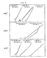
- Figure 2 is a graphical representation of the relative hardness of the coatings produced by the method of this invention versus the hydrocarbon-carrier ratio.
- Figure 3 is a graphical representation of the optical band gap for carbon and for silicon, both produced by glow discharge deposition.
- The invention herein contemplated includes a method of forming hard, carbonaceous tetrahedral like films and the hard films prepared thereby. The films are characterized by the absence of long range order. The disordered films are substantially equivalent to crystalline carbon films, and have a long range disordered structure of bent, intersecting, and puckered three-fold coordinated, graphitic lamina; with short range order including tetrahedral, four-fold carbon-carbon coordination, e.g., at intersections of graphitic planes, a low concentration of C-H bonds, and the substantial absence of linear polymers, on a substrate. The hard carbonaceous film is a carbon-hydrogen alloy formed by a process of decomposing a reaction gas containing at least gaseous hydrocarbon in a radio frequency maintained plasma, i.e., a glow discharge, and depositing the decomposition products on a substrate. The substrate may be a cold substrate; that is, it need not be externally heated.
- The preferred gaseous hydrocarbon are characterized by having carbon atoms tetrahedrally coordinated to carbon nearest neighbors through carbon-carbon bonds. It is believed that the tetrahedral coordination of carbon to carbon nearest neighbor atoms through carbon-carbon single bonds in the precursor gas acts as a template for the replication of four-fold carbon-carbon co-ordination in the deposited film. Exemplary gaseous hydrocarbons are x,x-dialkyls having the formula

where C represents a four-fold coordinated central carbon atom and C I, CII, C III and CIV represent methyl groups, alkyl groups, and mixtures thereof. A particularly preferred compound is 2,2-dimethyl propane having the formula
where C I, C II, CIII and CIV are all methyl groups. Other hydrocarbons having tetrahedrally coordinated central carbon atoms include 2,2-dimethyl butane, and 2,2,3,3-tetramethyl butane as well as higher homologs thereof. - It is believed that the presence of a halogen compound, especially a fluorine compound, in the reaction gas, e.g., a hydrocarbon gas, whether or not the hydrocarbon gas contains carbon atoms four-fold coordinated with other carbon atoms, enhances both tetrahedral coordination of carbon and the presence of an effective amount of hydrogen in the film. Moreover, the presence of hydrogen reduces the tendency of the fluorine to etch the deposit. When the halogen is fluorine. Suitable fluorine compounds include perfluorocarbons, e.g., CnF2n+2 where n is from 1 to about 8, and exemplified by carbon tetrafluoride, fluorinated hydrocarbons, e.g., C n F 2n+2-m H m where n is from 1 to about 8, and m is less than 2n+2, and exemplified by the fluoromethanes and fluoroethanes, and HF.
- According to the glow discharge method herein contemplated, the gaseous hydrocarbon (including the optional halogen, e.g. fluorocarbon) is in a gas mixture with inert gas. The inert gas may be helium, argon, neon, xenon or mixtures thereof. Preferably the inert gas is argon. The atomic ratio of the gaseous hydrocarbon to the carrier gas is from about 0.1:1.0 to about 10.0:1.0, depending on the desired properties of the deposited carbon film. As shown in Figure 2, hardness is a strong function of the ratio of hydrocarbon to argon. Thus, where the atomic ratio or volume ratio of hydrocarbon to argon is about 10:1, a relatively soft carbonaceous film is attained. When the volume ratio of hydrocarbon to argon is less than about 1.0/1, a relatively hard carbonaceous film is attained. When it is desired to obtain a relatively hard carbonaceous film, the volume ratio of hydrocarbon to argon is from about 0.1:1 to about 1:1.
- A method and apparatus for depositing the disordered carbon by glow discharge deposition are illustrated in Figure 1. The apparatus includes a
housing 10 having avacuum chamber 11 and aninlet chamber 12 and anoutlet chamber 13. Acathode backing member 14 is mounted in thevacuum chamber 11 through aninsulator 15 and is provided with an insulatingsleeve 16 and adark space shield 17. Asubstrate 18, i.e., a cathodically biased substrate, is secured to the inner end of thecathode backing member 14 by asubstrate holder 19 which may be joined to thecathode backing member 14 in electrical contact therewith. - The
cathode backing member 14 may be provided with a well receiving an electrical heater for heating thecathode backing member 14. However, this is not necessary as the disordered carbon films may be deposited at room temperature on the contemplated low temperature process. When thecathode backing member 14 has a well for receiving anelectrical heating element 20, thecathode backing member 14 may further have a temperatureresponsive probe 21, e.g., a thermocouple, for measuring the temperature of the cathode backing member. - The glow discharge decomposition apparatus further includes an
electrode 23 secured in thevacuum chamber 11 and spaced from thecathode backing member 14. Theelectrode 23 is provided with ashield 24. - The space in the
vacuum chamber 11 between thecathode backing member 14 and theelectrode 23 provides space for glow discharge conditions therebetween. In this way, there is produced a plasma within thevacuum chamber 11 between thecathode backing member 14 and the electrode. As herein contemplated, the cathode is electrically connected to a source of radio frequency power which may be regulated. Theelectrode 23 is grounded whereby to provide the desired glow discharge therebetween. - The
vacuum chamber 11 may be evacuated by avacuum pump 30 and particle trap 31 andpressure gauge 32 indicating the vacuum pressure in the vacuum chamber. - The
inlet chamber 12 of thehousing 10 may be provided with a plurality of conduits for introducing materials into thathousing 10. For example, in addition to the hydrocarbon gas, there may be provided fluorinated hydrocarbon gases or fluorocarbon gases whereby to provide fluorine in the deposited coating for substantially eliminating dangling bonds and providing a carbon-fluorine or carbon-fluorine-hydrogen alloy. - The
inlet chamber 12 may be located remote from thevacuum chamber 11 for premixing the gases before they are fed into thevacuum chamber 11 of the housing. Thus, the gases, as the hydrocarbon gas and the fluorocarbon gas, may be fed toconduit 34 through filters or purifyingdevices 35 through suitable control means 36. The control means controls the rate of admission of materials into thevacuum chamber 11. The materials fed through theconduit 34 and mixed in theinlet chamber 12 are subjected to the glow discharge composition between thecathode 14 and theelectrode 23 in thevacuum chamber 11. This provides the desired glow discharge decomposition and the formation of the disordered, diamond-like carbon on thesubstrate 18, optionally with the incorporation of the desired alterants or modifying elements therein as hydrogen and fluorine. - The method herein contemplated may also be carried where the substrate is a moving, continuous web, and the deposition is substantially continuous. For example, the process may be carried out with a deposition means including multichamber depositions, i.e., to provide a vertically arrayed structure.
- According to the method herein contemplated, the system is pumped down to a pressure less than about 5 x 10⁻⁸ torr prior to deposition.
- Thereafter, a hydrocarbon gas optionally with a carrier as an inert gas such as helium, argon, neon, or a mixture thereof, and optionally with fluorocarbon gases as tetrafluoromethane, (carbon tetrafluoride) difluoromethane or the like are fed into the
inlet chamber 12 through one of theconduits 34. The gas mixture is fed at a constant rate of about 100 standard cubic centimeters per minute total gas into thevacuum chamber 11. The vacuum chamber is maintained at a total pressure of about 50 to about 500 millitorrs and preferably from about 100-300 millitorr. - The partial pressure in the
vacuum chamber 11 of the gases introduced therein provides a reactive atmosphere which contains the hydrocarbon and fluorocarbon gases as well as the carrier gas, e.g., argon. A plasma is generated in the atmosphere between the electrode and the cathode using a radio frequency power of at least 50 watts and preferably up to 500 watts, operating at a radio frequency of from above about 0.1 megahertz, and generally for reasons of operational convenience, at about 13.56 megahertz. - By "radio frequency", also referred to herein as "r.f., is meant that portion of the electromagnetic spectrum having frequencies between the audio portion of the electromagnetic spectrum and the far infrared portion of the electromagnetic spectrum, i.e., from 0.1 megahertz to about 100 gigahertz, and wavelenghts corresponding thereto of from about 3 x 10³ meters for 0.1 megahertz radiation to 3 x 10⁻³ meter for 100 gigahertz radiation, and including "microwave" radiation.
- By "microwave" is meant that portion of radio frequency radiation having frequencies in the gigahertz range, i.e., above about 1 gigahertz (which is the generally accepted definition found in the IEEE Standard Dictionary of Electrical and Electronics Terms, F. Jay, editor, IEEE, New York, NY (1977) at page 416) and wavelengts corresponding thereto of less than about 3 x 10 1 meter for 1 gigahertz radiation. The upper range of microwave radiation is less than the frequencies and wavelengths of the "far infrared" portion of the electromagnetic spectrum.
- In the process, argon ions are attracted to the cathode and break the carbon hydrogen bonds. A subsequent carbon atom comes down to the substrate to take the place of the hydrogen. It is believed that the interaction of fluorine and hydrogen promotes the four-fold, tetrahedral, carbon-carbon coordination while avoiding etching by the fluorine.
- Additionally, the application of bias energy to raise the bonding levels in the carbon atoms,that is,to expand the normally available bonding orbitals, and enhances both the tetrahedral-likeness of the coating and the rate of film growth. The energy may be applied by applying a d.c. field or bias across the deposition electrodes, by applying an r.f. field across the deposition electrodes, or even by applying an ion beam to deposit film. Thus, an external ion beam may be directed onto the substrate and/or growing film during film deposition whereby to get ion bombardment during deposition.
- The process is carried out to form a coating of from about 100 angstroms to about 100 microns thick, and preferably from about 200 angstroms to about 20 microns in thickness. When coatings are prepared as described hereinabove, the disordered carbon coatings cannot be scratched with a steel or carbide scribe.
- The resulting deposited coatings, when subjected to Raman spectropscopy and to electron diffraction microscopy, indicated a disordered structure. Infrared spectropscopy indicated the low levels of C-H bonds, i.e., detectable by infrared spectroscopy and up to about 1 atomic percent of hydrogen.
- As the power applied to the plasma increases, i.e. from less than about 50 watts to 500 or more watts, the hydrogen in the deposit decreases, and the deposit gets darker and harder. Similarly, when the ratio of hydrocarbon gas to argon decreases, the hardness increases.
- The deposit is prepared at a low temperature, i.e., with the substrate at about 20° to 100°, although high temperatures may be utilized without deleterious effect.
- The method of the invention may be utilized to provide forming a hard carbonaceous film on a polymeric substrate. Suitable polymeric substrates include polycarbonates as General Electric "LEXAN", polyacrylates as stretched polyacrylates used in aircraft windows, and poly(allylcarbonate) as used in opthalmic and optical lenses.
- The method herein contemplated may also be used for forming hard carbonaceous films having semiconductor properties, e.g., a band edge, on a semiconductor device. The hard coating has an optical band gap intermediate that of graphite and of diamond, e.g., from about 0.1 to about 3.5 electron volts, and preferably from about 0.7 to 2.9 electron volts depending upon the deposition parameters and deposition gas concentration. As such, it may be used as an antireflective coating as well as an abrasion resistant coating on a photoresponsive semiconductor device. Particularly preferred is a deposit having an optical band gap of from about 1.3 to about 2.5 electron volts.
- The method herein contemplated may further be used to provide a hard carbonaceous film on a metallic substrate, for example, a substantially pin-hole free, corrosion resistant, surface or a semiconducting film on a conducting plate whereby to provide an electrostatic imaging surface.
- The following examples are illustrative of the method of this invention.
- A series of tests were carried out to compare glow discharge deposition of methane to glow discharge deposition of 2,2-dimethyl propane. In all cases, the deposit was formed by pumping a deposition chamber down to a pressure of less than 5 x 10⁻⁸ torr, forming a reaction gas of the gaseous hydrocarbon and argon, and passing the gaseous hydrocarbon through the vacuum chamber, with the sample on the cathode at the power indicated. The radio frequency was 13.56 megahertz.
- In the first test, methane was passed through the deposition chamber at a ratio of methane to argon of about 4/1. The deposition was carried out at a power of from about 50 watts. The deposit had an electrical resistance at 27° centigrade of about 6 x 10 12 (ohm centimeters), and an optical band gap of 2.2 electron volts.
- The above example was repeated at a power of about 50 watts and a ratio of methane to argon of about 1/1. The resulting film was a transparent-yellow, hard film with an electrical resistivity at 27°C of about 1 x 10¹⁰ (ohm-centimeters) and an optical band gap of 1.4 electron volts.
- The above example was repeated at a power of about 400 watts and a ratio of methane to argon about 1/1. The resulting film was black and substantially opaque and had an electrical resistivity of about 4 x 10⁶ (ohm-centimeters), and had an optical band gap of about 0.73 electron volts.
- Thereafter, the example was repeated with 2,2-dimethyl propane at a ratio of hydrocarbon to argon of 1/1 and a power of about 50 watts. The resulting surface was "soft", very transparent, had an electrical resistivity of above about 1012 (ohm centimeters), and had an optical band gap of about 2.9 electron volts.
- The run was repeated at a power of about 200 watts and a 2,2-dimethyl propane to argon ratio of about 0.1/1. The resulting surface was a hard surface having about 40 percent optical absorbtion at a thickness of 9000 angstroms, an electrical resistivity of about 1010 (ohm-centimeters), and an optical band gap of about 1.3 electron volts, and an index of refraction of 2.3 to 2.4.
- The above run was again repeated at a 2,2-dimethyl propane to argon ratio of about 0.25/1 and a radio frequency power of about 400 watts. The resulting film had an optical transmissivity of about 0 at 1 micron thickness, an electrical resisitivity of about 3 x 10⁸ (ohm centimeter), and an optical band gap of about 0.7 electron volt.
- Example I was repeated with a reaction gas of methane-carbon tetrafluoride-argon at a volume ratio of 9:10:10. Deposition was carried out at a power of 50 watts. The resulting film had an optical band gap of 2.0 electron volts.
- The above run was then repeated with a reaction gas having a methane-carbon tetafluoride-argon ration of 1:1:2. Deposition was carried out at a power of 50 watts. The resulting film had an optical band gap of 2.4 to 3.3 electron volts.
- The qualitative hardness data of Example I and II are reproduced in Figure 2.
- The optical band gap data of Examples I, II, and III are reproduced in Figure 3.
- While the invention has been described with respect to certain preferred exemplifications and embodiments thereof, it is not intended to limit the scope of the protection thereby but solely by the claims appended hereto.
Claims (21)
Applications Claiming Priority (2)
| Application Number | Priority Date | Filing Date | Title |
|---|---|---|---|
| US649324 | 1984-09-10 | ||
| US06/649,324 US4663183A (en) | 1984-09-10 | 1984-09-10 | Glow discharge method of applying a carbon coating onto a substrate |
Publications (2)
| Publication Number | Publication Date |
|---|---|
| EP0175980A2 true EP0175980A2 (en) | 1986-04-02 |
| EP0175980A3 EP0175980A3 (en) | 1987-04-01 |
Family
ID=24604312
Family Applications (1)
| Application Number | Title | Priority Date | Filing Date |
|---|---|---|---|
| EP85111221A Withdrawn EP0175980A3 (en) | 1984-09-10 | 1985-09-05 | Glow discharge method of applying a carbon coating onto a substrate and coating applied thereby |
Country Status (7)
| Country | Link |
|---|---|
| US (1) | US4663183A (en) |
| EP (1) | EP0175980A3 (en) |
| JP (1) | JPS6171626A (en) |
| KR (1) | KR860002249A (en) |
| AU (1) | AU567660B2 (en) |
| IL (1) | IL76336A0 (en) |
| PH (1) | PH22103A (en) |
Cited By (16)
| Publication number | Priority date | Publication date | Assignee | Title |
|---|---|---|---|---|
| EP0244874A2 (en) * | 1986-05-08 | 1987-11-11 | Kabushiki Kaisha Meidensha | Luminescent material, process for producing it and luminescent semiconductor device using it |
| EP0278480A2 (en) * | 1987-02-10 | 1988-08-17 | Semiconductor Energy Laboratory Co., Ltd. | Microwave enhanced cvd method for coating plastic articles with carbon film |
| US4777090A (en) * | 1986-11-03 | 1988-10-11 | Ovonic Synthetic Materials Company | Coated article and method of manufacturing the article |
| EP0304220A1 (en) * | 1987-08-10 | 1989-02-22 | Semiconductor Energy Laboratory Co., Ltd. | Thin film carbon material and method of depositing the same |
| US4843256A (en) * | 1986-12-23 | 1989-06-27 | Jenoptik Jena Gmbh | Controlled CMOS substrate voltage generator |
| US4849199A (en) * | 1987-03-30 | 1989-07-18 | Crystallume | Method for suppressing growth of graphite and other non-diamond carbon species during formation of synthetic diamond |
| US4859493A (en) * | 1987-03-31 | 1989-08-22 | Lemelson Jerome H | Methods of forming synthetic diamond coatings on particles using microwaves |
| EP0353934A1 (en) * | 1988-07-26 | 1990-02-07 | Fujikura Ltd. | Optical fiber and apparatus for producing same |
| EP0372696A2 (en) * | 1988-10-11 | 1990-06-13 | Semiconductor Energy Laboratory Co., Ltd. | Method of producing a carbon-based film |
| EP0384772A1 (en) * | 1989-02-24 | 1990-08-29 | McDONNELL DOUGLAS CORPORATION | Diamond like coating and a method of forming the same |
| EP0517627A1 (en) * | 1991-06-07 | 1992-12-09 | Eastman Kodak Company | Deposited carbon mask for dry etch processing of Si |
| EP0605814A1 (en) * | 1993-01-07 | 1994-07-13 | International Business Machines Corporation | Diamond-like carbon films from a hydrocarbon helium plasma |
| US6207281B1 (en) | 1988-03-07 | 2001-03-27 | Semiconductor Energy Laboratory Co., Ltd. | Electrostatic-erasing abrasion-proof coating and method for forming the same |
| US6224952B1 (en) | 1988-03-07 | 2001-05-01 | Semiconductor Energy Laboratory Co., Ltd. | Electrostatic-erasing abrasion-proof coating and method for forming the same |
| DE10111150A1 (en) * | 2001-02-15 | 2002-09-05 | Konrad Damasko | Clockwork assembly, especially for wrist or pocket watches, in which the working surfaces are coated with DLC (diamond like carbon) to largely prevent wear and thus make maintenance almost unnecessary |
| US6755566B2 (en) | 2001-02-15 | 2004-06-29 | Konrad Damasko | Clockwork |
Families Citing this family (72)
| Publication number | Priority date | Publication date | Assignee | Title |
|---|---|---|---|---|
| US5462772A (en) * | 1957-06-27 | 1995-10-31 | Lemelson; Jerome H. | Methods for forming artificial diamond |
| JPS61238961A (en) * | 1985-04-12 | 1986-10-24 | Sachiko Okazaki | Reforming method of base material surface |
| US6730244B1 (en) | 1986-01-28 | 2004-05-04 | Q2100, Inc. | Plastic lens and method for the production thereof |
| US5529728A (en) | 1986-01-28 | 1996-06-25 | Q2100, Inc. | Process for lens curing and coating |
| US5364256A (en) | 1986-01-28 | 1994-11-15 | Ophthalmic Research Group International, Inc. | Apparatus for the production of plastic lenses |
| US5415816A (en) | 1986-01-28 | 1995-05-16 | Q2100, Inc. | Method for the production of plastic lenses |
| US6201037B1 (en) | 1986-01-28 | 2001-03-13 | Ophthalmic Research Group International, Inc. | Plastic lens composition and method for the production thereof |
| JPS63140083A (en) * | 1986-05-29 | 1988-06-11 | Nippon Steel Corp | Stainless steel having black and transparent appearance and its production |
| DE3630419A1 (en) * | 1986-09-06 | 1988-03-10 | Kernforschungsanlage Juelich | METHOD FOR COATING COMPONENTS EXPOSED TO HIGH THERMAL LOADS WITH AN AMORPHOUS HYDROCARBON LAYER |
| JPS63107898A (en) * | 1986-10-23 | 1988-05-12 | Natl Inst For Res In Inorg Mater | Method for synthesizing diamond with plasma |
| US6083570A (en) * | 1987-03-31 | 2000-07-04 | Lemelson; Jerome H. | Synthetic diamond coatings with intermediate amorphous metal bonding layers and methods of applying such coatings |
| US5332348A (en) * | 1987-03-31 | 1994-07-26 | Lemelson Jerome H | Fastening devices |
| US4960643A (en) * | 1987-03-31 | 1990-10-02 | Lemelson Jerome H | Composite synthetic materials |
| US5096352A (en) * | 1987-03-31 | 1992-03-17 | Lemelson Jerome H | Diamond coated fasteners |
| JPH0672306B2 (en) * | 1987-04-27 | 1994-09-14 | 株式会社半導体エネルギー研究所 | Plasma processing apparatus and plasma processing method |
| US5230931A (en) * | 1987-08-10 | 1993-07-27 | Semiconductor Energy Laboratory Co., Ltd. | Plasma-assisted cvd of carbonaceous films by using a bias voltage |
| US5145711A (en) * | 1987-08-10 | 1992-09-08 | Semiconductor Energy Laboratory Co., Ltd. | Cyclotron resonance chemical vapor deposition method of forming a halogen-containing diamond on a substrate |
| FR2622337B1 (en) * | 1987-10-27 | 1995-06-16 | Thomson Csf | VIDEO RECORDING / PLAYING HEAD, METHOD FOR PRODUCING SAME AND APPARATUS IMPLEMENTING THE SAME |
| US5866195A (en) * | 1988-03-31 | 1999-02-02 | Lemelson; Jerome H. | Methods for forming diamond-coated superconductor wire |
| DE8909436U1 (en) * | 1988-08-04 | 1989-12-28 | Ion Tech Ltd., Teddington, Middlesex, Gb | |
| US5017403A (en) * | 1989-04-13 | 1991-05-21 | Massachusetts Institute Of Technology | Process for forming planarized films |
| DE69005938T2 (en) * | 1989-07-31 | 1994-05-19 | Matsushita Electric Ind Co Ltd | Device for producing a thin diamond-like carbon layer. |
| DE69021821T2 (en) * | 1989-09-20 | 1996-05-30 | Sumitomo Electric Industries | Process and plant for producing hard material. |
| KR930011413B1 (en) | 1990-09-25 | 1993-12-06 | 가부시키가이샤 한도오따이 에네루기 겐큐쇼 | Plasma cvd method for using pulsed waveform |
| JPH07109034B2 (en) * | 1991-04-08 | 1995-11-22 | ワイケイケイ株式会社 | Hard multilayer film forming body and method for producing the same |
| US5605759A (en) * | 1992-01-14 | 1997-02-25 | Prince; Robert | Physical vapor deposition of diamond-like carbon films |
| US5290610A (en) * | 1992-02-13 | 1994-03-01 | Motorola, Inc. | Forming a diamond material layer on an electron emitter using hydrocarbon reactant gases ionized by emitted electrons |
| US6500488B1 (en) * | 1992-08-04 | 2002-12-31 | Northwestern Univ. | Method of forming fluorine-bearing diamond layer on substrates, including tool substrates |
| US5794801A (en) * | 1993-08-16 | 1998-08-18 | Lemelson; Jerome | Material compositions |
| US5514214A (en) | 1993-09-20 | 1996-05-07 | Q2100, Inc. | Eyeglass lens and mold spin coater |
| US5688556A (en) * | 1994-04-01 | 1997-11-18 | Mobil Oil Corporation | Barrier films having vapor coated EVOH surfaces |
| US5464667A (en) * | 1994-08-16 | 1995-11-07 | Minnesota Mining And Manufacturing Company | Jet plasma process and apparatus |
| EP0743375B1 (en) * | 1995-03-31 | 2000-07-12 | CeramOptec GmbH | Method of producing diamond-like-carbon coatings |
| US5714202A (en) * | 1995-06-07 | 1998-02-03 | Lemelson; Jerome H. | Synthetic diamond overlays for gas turbine engine parts having thermal barrier coatings |
| US5688557A (en) * | 1995-06-07 | 1997-11-18 | Lemelson; Jerome H. | Method of depositing synthetic diamond coatings with intermediates bonding layers |
| US5616372A (en) * | 1995-06-07 | 1997-04-01 | Syndia Corporation | Method of applying a wear-resistant diamond coating to a substrate |
| US5871805A (en) * | 1996-04-08 | 1999-02-16 | Lemelson; Jerome | Computer controlled vapor deposition processes |
| US6022498A (en) | 1996-04-19 | 2000-02-08 | Q2100, Inc. | Methods for eyeglass lens curing using ultraviolet light |
| US6280171B1 (en) | 1996-06-14 | 2001-08-28 | Q2100, Inc. | El apparatus for eyeglass lens curing using ultraviolet light |
| US6203898B1 (en) | 1997-08-29 | 2001-03-20 | 3M Innovatave Properties Company | Article comprising a substrate having a silicone coating |
| KR100477402B1 (en) * | 1997-11-20 | 2005-03-22 | 동경 엘렉트론 주식회사 | Method of forming film by plasma |
| GB2338716B (en) * | 1998-06-26 | 2003-04-02 | Mclaughlin James A | An apparatus and a method for coating diamond like carbon (DLC) or other vacuum depositable coatings onto a substrate |
| US6287711B1 (en) | 1998-07-01 | 2001-09-11 | Front Edge Technology, Inc. | Wear-resistant coating and component |
| KR100307629B1 (en) * | 1999-04-30 | 2001-09-26 | 윤종용 | Method for forming and applicating a anti reflective film using hydrocarbon based gas |
| US6749813B1 (en) | 2000-03-05 | 2004-06-15 | 3M Innovative Properties Company | Fluid handling devices with diamond-like films |
| US6795636B1 (en) | 2000-03-05 | 2004-09-21 | 3M Innovative Properties Company | Radiation-transmissive films on glass articles |
| EP1158088A3 (en) * | 2000-05-26 | 2003-01-22 | Voith Paper Patent GmbH | Process and device for treating a fibrous suspension |
| US7106939B2 (en) * | 2001-09-19 | 2006-09-12 | 3M Innovative Properties Company | Optical and optoelectronic articles |
| US7866342B2 (en) | 2002-12-18 | 2011-01-11 | Vapor Technologies, Inc. | Valve component for faucet |
| US8555921B2 (en) | 2002-12-18 | 2013-10-15 | Vapor Technologies Inc. | Faucet component with coating |
| US7866343B2 (en) | 2002-12-18 | 2011-01-11 | Masco Corporation Of Indiana | Faucet |
| US8220489B2 (en) | 2002-12-18 | 2012-07-17 | Vapor Technologies Inc. | Faucet with wear-resistant valve component |
| US6904935B2 (en) | 2002-12-18 | 2005-06-14 | Masco Corporation Of Indiana | Valve component with multiple surface layers |
| US8679674B2 (en) * | 2005-03-25 | 2014-03-25 | Front Edge Technology, Inc. | Battery with protective packaging |
| US7846579B2 (en) | 2005-03-25 | 2010-12-07 | Victor Krasnov | Thin film battery with protective packaging |
| US20070026205A1 (en) | 2005-08-01 | 2007-02-01 | Vapor Technologies Inc. | Article having patterned decorative coating |
| US7862927B2 (en) * | 2007-03-02 | 2011-01-04 | Front Edge Technology | Thin film battery and manufacturing method |
| US20080260968A1 (en) * | 2007-04-23 | 2008-10-23 | Atto Co., Ltd. | Method of forming amorphous carbon layer using cross type hydrocarbon compound and method of forming low-k dielectric layer using the same |
| US8870974B2 (en) * | 2008-02-18 | 2014-10-28 | Front Edge Technology, Inc. | Thin film battery fabrication using laser shaping |
| US7862627B2 (en) | 2007-04-27 | 2011-01-04 | Front Edge Technology, Inc. | Thin film battery substrate cutting and fabrication process |
| US8628645B2 (en) * | 2007-09-04 | 2014-01-14 | Front Edge Technology, Inc. | Manufacturing method for thin film battery |
| US20090136839A1 (en) * | 2007-11-28 | 2009-05-28 | Front Edge Technology, Inc. | Thin film battery comprising stacked battery cells and method |
| US8502494B2 (en) * | 2009-08-28 | 2013-08-06 | Front Edge Technology, Inc. | Battery charging apparatus and method |
| US8865340B2 (en) | 2011-10-20 | 2014-10-21 | Front Edge Technology Inc. | Thin film battery packaging formed by localized heating |
| US9887429B2 (en) | 2011-12-21 | 2018-02-06 | Front Edge Technology Inc. | Laminated lithium battery |
| US8864954B2 (en) | 2011-12-23 | 2014-10-21 | Front Edge Technology Inc. | Sputtering lithium-containing material with multiple targets |
| US9077000B2 (en) | 2012-03-29 | 2015-07-07 | Front Edge Technology, Inc. | Thin film battery and localized heat treatment |
| US9257695B2 (en) | 2012-03-29 | 2016-02-09 | Front Edge Technology, Inc. | Localized heat treatment of battery component films |
| US9159964B2 (en) | 2012-09-25 | 2015-10-13 | Front Edge Technology, Inc. | Solid state battery having mismatched battery cells |
| US8753724B2 (en) | 2012-09-26 | 2014-06-17 | Front Edge Technology Inc. | Plasma deposition on a partially formed battery through a mesh screen |
| US9356320B2 (en) | 2012-10-15 | 2016-05-31 | Front Edge Technology Inc. | Lithium battery having low leakage anode |
| US10008739B2 (en) | 2015-02-23 | 2018-06-26 | Front Edge Technology, Inc. | Solid-state lithium battery with electrolyte |
Citations (3)
| Publication number | Priority date | Publication date | Assignee | Title |
|---|---|---|---|---|
| EP0064760A1 (en) * | 1981-05-12 | 1982-11-17 | Meidensha Electric Mfg. Co., Ltd. | Hydrogen-containing silicic substance, process for producing the same, and use thereof |
| JPS5930709A (en) * | 1982-08-13 | 1984-02-18 | Toa Nenryo Kogyo Kk | Method for synthesizing carbon film and carbon granule in vapor phase |
| US4434188A (en) * | 1981-12-17 | 1984-02-28 | National Institute For Researches In Inorganic Materials | Method for synthesizing diamond |
Family Cites Families (6)
| Publication number | Priority date | Publication date | Assignee | Title |
|---|---|---|---|---|
| GB1582231A (en) * | 1976-08-13 | 1981-01-07 | Nat Res Dev | Application of a layer of carbonaceous material to a surface |
| DE3175345D1 (en) * | 1980-08-21 | 1986-10-23 | Nat Res Dev | Coating insulating materials by glow discharge |
| US4522663A (en) * | 1980-09-09 | 1985-06-11 | Sovonics Solar Systems | Method for optimizing photoresponsive amorphous alloys and devices |
| US4402993A (en) * | 1981-03-20 | 1983-09-06 | Gulf & Western Manufacturing Company | Process for coating optical fibers |
| DE3205345A1 (en) * | 1982-02-15 | 1983-09-01 | Philips Patentverwaltung Gmbh, 2000 Hamburg | "METHOD FOR THE PRODUCTION OF FLUOREDOTED LIGHT-CONDUCTING FIBERS" |
| US4517223A (en) * | 1982-09-24 | 1985-05-14 | Sovonics Solar Systems | Method of making amorphous semiconductor alloys and devices using microwave energy |
-
1984
- 1984-09-10 US US06/649,324 patent/US4663183A/en not_active Expired - Fee Related
-
1985
- 1985-09-04 AU AU47076/85A patent/AU567660B2/en not_active Ceased
- 1985-09-05 EP EP85111221A patent/EP0175980A3/en not_active Withdrawn
- 1985-09-09 PH PH32750A patent/PH22103A/en unknown
- 1985-09-09 IL IL76336A patent/IL76336A0/en unknown
- 1985-09-10 JP JP60200402A patent/JPS6171626A/en active Pending
- 1985-09-10 KR KR1019850006598A patent/KR860002249A/en not_active Application Discontinuation
Patent Citations (3)
| Publication number | Priority date | Publication date | Assignee | Title |
|---|---|---|---|---|
| EP0064760A1 (en) * | 1981-05-12 | 1982-11-17 | Meidensha Electric Mfg. Co., Ltd. | Hydrogen-containing silicic substance, process for producing the same, and use thereof |
| US4434188A (en) * | 1981-12-17 | 1984-02-28 | National Institute For Researches In Inorganic Materials | Method for synthesizing diamond |
| JPS5930709A (en) * | 1982-08-13 | 1984-02-18 | Toa Nenryo Kogyo Kk | Method for synthesizing carbon film and carbon granule in vapor phase |
Non-Patent Citations (4)
| Title |
|---|
| 4ème COLLOQUE INTERNATIONAL SUR LES PLASMAS ET LA PULVERISATION CATHODIQUE C.I.P. 82, 13th-17th September 1982, pages 163-168, I.U.T., Nice, FR; A.R. NYAIESH et al.: "Amorphous hard carbon films on polycarbonate substrates" * |
| CHEMICAL ABSTRACTS, vol. 92, no. 24, June 1980, page 112, abstract no. 200300j, Columbus, Ohio, US; S. OTANI et al.: "Preparation of pyrolytic carbons from cis-1,2-dichloroethylene and their structure", & PROC. LONDON INT. CARBON GRAPHITE CONF. 5th 1978, 2, 811-15 * |
| PATENTS ABSTRACTS OF JAPAN, vol. 8, no. 118 (C-226)[1555], 31 may 1984; & JP 59030709 A (TOA NENRYO KOGYO K.K.) 18-02-1984 * |
| THIN SOLID FILMS, vol. 63, 1979, pages 155-160, Elsevier Sequoia S.A., Lausanne - printed in the Netherlands, CH; L.P. ANDERSSON et al.: "Properties and coating rates of diamond-like carbon films produced by R.F. Glow discharge of hydrocarbon gases" * |
Cited By (24)
| Publication number | Priority date | Publication date | Assignee | Title |
|---|---|---|---|---|
| EP0244874A2 (en) * | 1986-05-08 | 1987-11-11 | Kabushiki Kaisha Meidensha | Luminescent material, process for producing it and luminescent semiconductor device using it |
| EP0244874A3 (en) * | 1986-05-08 | 1988-10-12 | Kabushiki Kaisha Meidensha | Luminescent material, process for producing it and luminescent semiconductor device using it |
| US4777090A (en) * | 1986-11-03 | 1988-10-11 | Ovonic Synthetic Materials Company | Coated article and method of manufacturing the article |
| US4843256A (en) * | 1986-12-23 | 1989-06-27 | Jenoptik Jena Gmbh | Controlled CMOS substrate voltage generator |
| EP0278480A2 (en) * | 1987-02-10 | 1988-08-17 | Semiconductor Energy Laboratory Co., Ltd. | Microwave enhanced cvd method for coating plastic articles with carbon film |
| EP0278480A3 (en) * | 1987-02-10 | 1989-02-22 | Semiconductor Energy Laboratory Co., Ltd. | Microwave enhanced cvd method for coating plastic articles with carbon film and its products |
| US4849199A (en) * | 1987-03-30 | 1989-07-18 | Crystallume | Method for suppressing growth of graphite and other non-diamond carbon species during formation of synthetic diamond |
| US4859493A (en) * | 1987-03-31 | 1989-08-22 | Lemelson Jerome H | Methods of forming synthetic diamond coatings on particles using microwaves |
| EP0304220A1 (en) * | 1987-08-10 | 1989-02-22 | Semiconductor Energy Laboratory Co., Ltd. | Thin film carbon material and method of depositing the same |
| US6207281B1 (en) | 1988-03-07 | 2001-03-27 | Semiconductor Energy Laboratory Co., Ltd. | Electrostatic-erasing abrasion-proof coating and method for forming the same |
| US6224952B1 (en) | 1988-03-07 | 2001-05-01 | Semiconductor Energy Laboratory Co., Ltd. | Electrostatic-erasing abrasion-proof coating and method for forming the same |
| US7144629B2 (en) | 1988-03-07 | 2006-12-05 | Semiconductor Energy Laboratory Co., Ltd. | Electrostatic-erasing abrasion-proof coating and method for forming the same |
| US6265070B1 (en) | 1988-03-07 | 2001-07-24 | Semiconductor Energy Laboratory Co., Ltd. | Electrostatic-erasing abrasion-proof coating and method for forming the same |
| US4964694A (en) * | 1988-07-26 | 1990-10-23 | Fujikura Ltd. | Optical fiber and apparatus for producing same |
| EP0481570A3 (en) * | 1988-07-26 | 1992-09-02 | Fujikura Ltd. | Optical fiber and apparatus for producing same |
| EP0353934A1 (en) * | 1988-07-26 | 1990-02-07 | Fujikura Ltd. | Optical fiber and apparatus for producing same |
| US5185179A (en) * | 1988-10-11 | 1993-02-09 | Semiconductor Energy Laboratory Co., Ltd. | Plasma processing method and products thereof |
| EP0372696A2 (en) * | 1988-10-11 | 1990-06-13 | Semiconductor Energy Laboratory Co., Ltd. | Method of producing a carbon-based film |
| EP0372696A3 (en) * | 1988-10-11 | 1990-07-18 | Semiconductor Energy Laboratory Co., Ltd. | Method of producing a carbon-based film |
| EP0384772A1 (en) * | 1989-02-24 | 1990-08-29 | McDONNELL DOUGLAS CORPORATION | Diamond like coating and a method of forming the same |
| EP0517627A1 (en) * | 1991-06-07 | 1992-12-09 | Eastman Kodak Company | Deposited carbon mask for dry etch processing of Si |
| EP0605814A1 (en) * | 1993-01-07 | 1994-07-13 | International Business Machines Corporation | Diamond-like carbon films from a hydrocarbon helium plasma |
| DE10111150A1 (en) * | 2001-02-15 | 2002-09-05 | Konrad Damasko | Clockwork assembly, especially for wrist or pocket watches, in which the working surfaces are coated with DLC (diamond like carbon) to largely prevent wear and thus make maintenance almost unnecessary |
| US6755566B2 (en) | 2001-02-15 | 2004-06-29 | Konrad Damasko | Clockwork |
Also Published As
| Publication number | Publication date |
|---|---|
| AU567660B2 (en) | 1987-11-26 |
| EP0175980A3 (en) | 1987-04-01 |
| US4663183A (en) | 1987-05-05 |
| JPS6171626A (en) | 1986-04-12 |
| IL76336A0 (en) | 1986-01-31 |
| AU4707685A (en) | 1986-03-27 |
| KR860002249A (en) | 1986-04-24 |
| PH22103A (en) | 1988-05-20 |
Similar Documents
| Publication | Publication Date | Title |
|---|---|---|
| US4663183A (en) | Glow discharge method of applying a carbon coating onto a substrate | |
| US4770940A (en) | Glow discharge method of applying a carbon coating onto a substrate and coating applied thereby | |
| US5198263A (en) | High rate chemical vapor deposition of carbon films using fluorinated gases | |
| EP0238085B1 (en) | Improved diamond-like carbon films and process for production thereof | |
| US5055421A (en) | Method for the plasma deposition of hydrogenated, amorphous carbon using predetermined retention times of gaseous hydrocarbons | |
| EP0304220B1 (en) | Thin film carbon material and method of depositing the same | |
| Saito et al. | Diamond-like carbon films prepared from CH 4-H 2-H 2 O mixed gas using a microwave plasma | |
| Maeda et al. | Diamond growth from a mixture of fluorocarbon and hydrogen in a microwave plasma | |
| Shimada et al. | Analysis of diamond phase in hydrogenated hard carbon film using radio frequency plasma etching | |
| John et al. | IR attenuated total reflectance studies of dc biased growth of diamond films | |
| CA1332720C (en) | Production of polymer-metal compounds and the production of said compounds by discharge in the glow-discharge zones | |
| EP0617141B1 (en) | Improved method for growing continuous diamond films | |
| JPH0421638B2 (en) | ||
| Guo et al. | Evaluation of carbon films electrodeposited on different substrates from different organic solvents | |
| Jubber et al. | Atom beam treatment of diamond films | |
| Ianno et al. | Plasma-enhanced chemical vapor deposition of molybdenum | |
| Loh et al. | Growth studies of thin film diamond using molecular beam techniques | |
| Jubber et al. | Microwave plasma chemical vapour deposition of high purity diamond films | |
| Manage | Structural and optical characterization of hydrogenated amorphous carbon thin films. | |
| McNamara et al. | Comparison of Tantalum and Rhenium Filaments in Diamond CVD Using Selective Carbon‐13 Labeling | |
| RU2099283C1 (en) | Diamond-like carbon-based coating and method of manufacturing thereof | |
| Hirabayashi et al. | Epitaxial growth of cubic SiC by hot filament CVD | |
| Athwal et al. | Dlc films by plasma assisted chemical vapor deposition near room temperature | |
| KR0156562B1 (en) | A method for preparing an electrophotographic photoreceptor | |
| Huck et al. | Mass-separated ion beam deposition of diamond-like thin films |
Legal Events
| Date | Code | Title | Description |
|---|---|---|---|
| PUAI | Public reference made under article 153(3) epc to a published international application that has entered the european phase |
Free format text: ORIGINAL CODE: 0009012 |
|
| AK | Designated contracting states |
Kind code of ref document: A2 Designated state(s): AT BE CH DE FR GB IT LI LU NL SE |
|
| PUAL | Search report despatched |
Free format text: ORIGINAL CODE: 0009013 |
|
| AK | Designated contracting states |
Kind code of ref document: A3 Designated state(s): AT BE CH DE FR GB IT LI LU NL SE |
|
| RAP1 | Party data changed (applicant data changed or rights of an application transferred) |
Owner name: OVONIC SYNTHETIC MATERIALS COMPANY, INC. |
|
| 17P | Request for examination filed |
Effective date: 19870728 |
|
| 17Q | First examination report despatched |
Effective date: 19890202 |
|
| STAA | Information on the status of an ep patent application or granted ep patent |
Free format text: STATUS: THE APPLICATION IS DEEMED TO BE WITHDRAWN |
|
| 18D | Application deemed to be withdrawn |
Effective date: 19890613 |
|
| RIN1 | Information on inventor provided before grant (corrected) |
Inventor name: FLASCK, JAMES Inventor name: OVSHINSKY, STANFORD R. |