EP0176356A2 - Photosensitive polymer compositions, electrophoretic deposition processes using same, and the use of same in forming films on substrates - Google Patents
Photosensitive polymer compositions, electrophoretic deposition processes using same, and the use of same in forming films on substrates Download PDFInfo
- Publication number
- EP0176356A2 EP0176356A2 EP85306800A EP85306800A EP0176356A2 EP 0176356 A2 EP0176356 A2 EP 0176356A2 EP 85306800 A EP85306800 A EP 85306800A EP 85306800 A EP85306800 A EP 85306800A EP 0176356 A2 EP0176356 A2 EP 0176356A2
- Authority
- EP
- European Patent Office
- Prior art keywords
- polymer
- film
- composition
- photosensitive
- groups
- Prior art date
- Legal status (The legal status is an assumption and is not a legal conclusion. Google has not performed a legal analysis and makes no representation as to the accuracy of the status listed.)
- Granted
Links
Images
Classifications
-
- G—PHYSICS
- G03—PHOTOGRAPHY; CINEMATOGRAPHY; ANALOGOUS TECHNIQUES USING WAVES OTHER THAN OPTICAL WAVES; ELECTROGRAPHY; HOLOGRAPHY
- G03F—PHOTOMECHANICAL PRODUCTION OF TEXTURED OR PATTERNED SURFACES, e.g. FOR PRINTING, FOR PROCESSING OF SEMICONDUCTOR DEVICES; MATERIALS THEREFOR; ORIGINALS THEREFOR; APPARATUS SPECIALLY ADAPTED THEREFOR
- G03F7/00—Photomechanical, e.g. photolithographic, production of textured or patterned surfaces, e.g. printing surfaces; Materials therefor, e.g. comprising photoresists; Apparatus specially adapted therefor
- G03F7/004—Photosensitive materials
- G03F7/027—Non-macromolecular photopolymerisable compounds having carbon-to-carbon double bonds, e.g. ethylenic compounds
- G03F7/028—Non-macromolecular photopolymerisable compounds having carbon-to-carbon double bonds, e.g. ethylenic compounds with photosensitivity-increasing substances, e.g. photoinitiators
-
- G—PHYSICS
- G03—PHOTOGRAPHY; CINEMATOGRAPHY; ANALOGOUS TECHNIQUES USING WAVES OTHER THAN OPTICAL WAVES; ELECTROGRAPHY; HOLOGRAPHY
- G03F—PHOTOMECHANICAL PRODUCTION OF TEXTURED OR PATTERNED SURFACES, e.g. FOR PRINTING, FOR PROCESSING OF SEMICONDUCTOR DEVICES; MATERIALS THEREFOR; ORIGINALS THEREFOR; APPARATUS SPECIALLY ADAPTED THEREFOR
- G03F7/00—Photomechanical, e.g. photolithographic, production of textured or patterned surfaces, e.g. printing surfaces; Materials therefor, e.g. comprising photoresists; Apparatus specially adapted therefor
- G03F7/004—Photosensitive materials
- G03F7/027—Non-macromolecular photopolymerisable compounds having carbon-to-carbon double bonds, e.g. ethylenic compounds
-
- C—CHEMISTRY; METALLURGY
- C25—ELECTROLYTIC OR ELECTROPHORETIC PROCESSES; APPARATUS THEREFOR
- C25D—PROCESSES FOR THE ELECTROLYTIC OR ELECTROPHORETIC PRODUCTION OF COATINGS; ELECTROFORMING; APPARATUS THEREFOR
- C25D5/00—Electroplating characterised by the process; Pretreatment or after-treatment of workpieces
-
- G—PHYSICS
- G03—PHOTOGRAPHY; CINEMATOGRAPHY; ANALOGOUS TECHNIQUES USING WAVES OTHER THAN OPTICAL WAVES; ELECTROGRAPHY; HOLOGRAPHY
- G03F—PHOTOMECHANICAL PRODUCTION OF TEXTURED OR PATTERNED SURFACES, e.g. FOR PRINTING, FOR PROCESSING OF SEMICONDUCTOR DEVICES; MATERIALS THEREFOR; ORIGINALS THEREFOR; APPARATUS SPECIALLY ADAPTED THEREFOR
- G03F7/00—Photomechanical, e.g. photolithographic, production of textured or patterned surfaces, e.g. printing surfaces; Materials therefor, e.g. comprising photoresists; Apparatus specially adapted therefor
- G03F7/16—Coating processes; Apparatus therefor
- G03F7/164—Coating processes; Apparatus therefor using electric, electrostatic or magnetic means; powder coating
-
- Y—GENERAL TAGGING OF NEW TECHNOLOGICAL DEVELOPMENTS; GENERAL TAGGING OF CROSS-SECTIONAL TECHNOLOGIES SPANNING OVER SEVERAL SECTIONS OF THE IPC; TECHNICAL SUBJECTS COVERED BY FORMER USPC CROSS-REFERENCE ART COLLECTIONS [XRACs] AND DIGESTS
- Y10—TECHNICAL SUBJECTS COVERED BY FORMER USPC
- Y10S—TECHNICAL SUBJECTS COVERED BY FORMER USPC CROSS-REFERENCE ART COLLECTIONS [XRACs] AND DIGESTS
- Y10S430/00—Radiation imagery chemistry: process, composition, or product thereof
- Y10S430/138—Corona discharge process
Definitions
- This invention is concerned with photosensitive polymer compositions and their use in electrophoretic deposition processes, for example, to deposit on a conductive surface a uniform, negative-acting, aqueous-developable photoresist film that is resistant to strong inorganic acids and aqueous bases.
- Photoresists are photosensitive films capable of transferring an image onto a conductive surface, for example, the metal surface of a printed circuit board or lithographic plate.
- Liquid-type photoresists typically contain a combination of a film-forming resin or polymer and a photosensitive compound or photoinitiator dissolved or suspended in a solvent such as an organic liquid.
- Liquid-type photoresists can be negative-acting or positive-acting systems.
- a negative-acting photoresist or negative resist after the film is deposited on a surface and the solvent is removed, e.g. by heating, the film is selectively exposed, typically through a photomask, to a source of energy, such as ultraviolet light.
- the photomask has areas that are opaque and other areas that are transparent to the exposing radiation.
- the pattern on the photomask formed by the opaque and transparent areas defines the desired image, for example, a circuit, which is to be transferred to the substrate surface.
- the exposed portions of a negative resist film become less soluble in a developing solution than the unexposed portions, as the result of a photochemical reaction between the photoinitiator and the polymer or resin upon exposure. This difference in solubility allows for the selective removal of the unexposed film and the transfer of the image to the surface.
- the exposed portions of the film become more soluble than the unexposed portions in the developer, as a result of the photochemical reaction, allowing for the selective removal of the exposed areas.
- the portions of the surface that are not protected by the resist may be etched, such as by the action of an oxidizing solution typically containing an inorganic acid. The remaining resist film may then be stripped from the surface leaving only the desired etched image on the substrate.
- a metallic substrate surface containing the imaged resist can be plated with a metal or combination of metals, for example, tin and lead. The resist may then be stripped and the exposed substrate metal may be etched to form the desired pattern or a circuit on the substrate surface.
- a metal or combination of metals for example, tin and lead.
- the resist may then be stripped and the exposed substrate metal may be etched to form the desired pattern or a circuit on the substrate surface.
- liquid-type resists have been used for many years in lithographic and electronics applications, and despite numerous improvements to the resist systems and processing steps involved with their use, these conventional liquid resists still suffer from one or more disadvantages.
- special surface preparations may be required to obtain good adhesion of a liquid resist film onto a surface. This increases the processing time and cost involved.
- the resists themselves may also require other special processing steps, such as hardening or baking steps, which also increase processing time.
- the cost of the resist components utilized in conventional systems combined with the loss of materials in depositing a film and the difficulty in reproducibly synthesizing stable systems, has also been a problem.
- Dry film type resists are multilayer films in which the photoresist is precast into a solid film and sandwiched between a polyethylene film and a polyester cover sheet. Dry film resists are described in U.S. Patent Nos. 3,469,982, 4,378,264 and 4,343,885.
- the lamination, onto the surface of a printed circuit board, of the photoresist layer of a dry film resist is typically achieved by peeling away the polyethylene film layer from the adjacent photoresist layer and then bringing the thus exposed surface of the photoresist layer of the resulting photoresist layer/cover sheet combination into contact with the surface of the printed circuit board onto which the photoresist layer is to be laminated.
- the photoresist layer/cover sheet combination is then laminated onto the printed circuit board, for example, using hot rollers.
- the transparent cover sheet which provides mechanical support for the photoresist film layer, is usually kept in place until after the photoresist is exposed through a photomask and the cover sheet. After exposure, the cover sheet is peeled away from the resist film and the resist is developed and processed in a conventional manner.
- dry film resists also suffer from a number of drawbacks.
- the conductive copper surface of a printed circuit board contains a protective coating, known as a chromate conversion coating, that protects the copper from oxidation. Therefore, before a dry film resist can be applied to the metal surface, the conversion coating must be removed, for example, by abrasive scrubbing. This scrubbing roughens the surface and facilitates adhesion of the dry film resist to the substrate surface.
- an abrasive scrubber can lead to defective circuitry on subsequent etching operations.
- Dry film resists may also have difficulty in adhering to metal surfaces unless the metal has been specially prepared.
- dry film resists typically cannot be used effectively with surfaces having irregular topographies. For example, a small scratch in the substrate surface may not be filled by a dry film resist. The dry film may merely bridge the scratch and can allow etchant to seep into the scratch during etching resulting in unacceptable circuits.
- their use also results in substantial waste of materials in the form of unusable strips of excess film because the dry film resists are typically trimmed to conform with the substrate surface to be coated.
- Electrophoresis refers to the motion of charged particles or molecules through a liquid medium under the influence of an applied electrical field. Electrophoretic deposition or electrodeposition is conducted in an electrolytic cell where the surface of the conductive material, to be coated by the migrating charged particles, serves as one electrode. Polymers bearing a positive charge in the liquid medium, or polymers which become associated with a substance such as a surfactant having a positive charge, are known as cationic polymers. The electrodeposition of cationic polymers on the surface of a negatively charged electrode (cathode) is referred to as cataphoresis, while the electrophoretic deposition of negatively charged polymers (anionic polymers) onto the surface of a positively charged electrode (anode) is known as anaphoresis.
- Electrophoresis has been used to prepare electrical components, such as resistors and capacitors, that are integral to printed circuit boards (U.S. Patent No. 3,303,078).
- U.S. Patent No. 3,403,088 is directed to anaphoresis of water-dispersed acrylic interpolymers to prepare thermally curable, non-photoactive, insulating coatings for electrical devices.
- U.S. Patent No. 3,446,723 is also directed to thermally cured, non-photoactive, coatings preferably applied by cataphoresis. Cataphoresis is taught in U.S. Patent No.
- Electrophoretic deposition of photosensitive coatings is also generally known.
- U.S. Patent No. 3,738,835 describes the use of anaphoresis to deposit a photosensitive composition from an emulsion prepared from a solution containing a polychloroprene polymer, a photosensitizer, such as 4,4'-bis-(dimethyl-amino)-benzophenone, a stabilizer, such as hydroquinone that prevents the unsaturated polymer from decomposing in solution, and a hardener such as a partially cured resin or other polymer to provide etch resistance, in an 80% butyl acetate/20% methyl ethyl ketone or 80% cyclohexanone/20% methyl ethyl ketone solvent, the percentages being percentages by volume.
- the emulsion is formed by the addition, to this solution, of an aqueous solution containing a wetting agent, such as a fluorocarbon anionic surfactant, N-methyl-2-pyrolidone and triethyl amine.
- a wetting agent such as a fluorocarbon anionic surfactant, N-methyl-2-pyrolidone and triethyl amine.
- the unsaturated polymer crosslinks and the unexposed film is developed with an organic solvent.
- U.S. Patents Nos. 3,954,587; 4,029,561; 4,035,273; 4,035,274; 4,039,414; 4,066,523; 4,070,258; and 4,166,017 also disclose coatings that are applied by electrophoresis and are cured by exposure to ultraviolet (UV) light and/or heat.
- UV ultraviolet
- U.S. Patent No. 3,844,919 relates to the electrodeposition of a permanent photoconductive material prepared from a photoconductive zinc oxide, an electrically insulating resin, such as an acrylic resin, and an organic solvent or water.
- U.S. Patent No. 4,414,311 describes the preparation of lithographic printing plates by cataphoretically applying a thin, submicrometre photosensitive film, from an aqueous solution of a polymeric material having pendant diazonium salts, onto an electrochemically hydrophilized metal surface.
- the thin film is exposed to UV radiation, developed and inked to form a lithographic printing plate.
- Japanese patent application 77-11601 describes electrophoretically depositing a photosensitive polymer composition onto a silicate coated metal surface.
- the photosensitive polymers are soluble or dispersible in an aqueous medium and capable of being anaphoretically deposited on a conductive surface by virtue of containing neutralized acid groups.
- the polymers are photosensitive by virtue of containing unsaturated groups that crosslink upon exposure to light.
- the preparation of these polymers requires at least two steps; the first step being the preparation of a polymer having unsaturated groups or acid groups and the second step being either the addition of an acid to a polymer having unsaturated groups or the addition of unsaturated groups to a polymer having acid groups.
- This Japanese patent application illustrates the formation of such polymers from an acrylic polymer having acid groups and pendant hydroxy groups and an isocyanate-containing methacrylate compound.
- the preparation of these photosensitive polymers is difficult because of the number of separate reactions needed.
- the extent to which such polymers can be effectively crosslinked is limited by the number of available unsaturated groups on the polymer or the number of unsaturated groups that can be attached thereto.
- the number of unsaturated groups that can be attached to the polymer may also affect other desirable properties of the resist such as its aqueous solubility and capability to form high quality films.
- photosensitive compositions containing a neutralized acid group are not capable of being used in a cataphoretic deposition process and while the patent mentions cataphoresis, it fails to suggest any composition that can be used to cataphoretically form an aqueous acid- developable and strippable resist that is resistant to aqueous base solutions and inorganic acids.
- Japanese patent disclosure 55(1980)-148491 entitled Method for Preparing Printed Wiring Boards discloses using electrophoresis for coating photosensitive substances onto the copper surface of a copper-laminated plate in preparing printed circuit boards.
- this reference does not describe any materials useful for the process or any of the process conditions used therein.
- the present invention may enable the provision of photosensitive polymer compositions which are capable of being electrophoretically deposited from an aqueous solution or emulsion directly onto a conductive surface, for example as a uniform, adherent, photosensitive film of desired thickness, and which may solve the problems of conventional liquid-type and dry film resists.
- the photosensitive polymer compositions may be electrophoretically deposited as a uniform film of desired thickness on a conductive surface of regular or irregular surface topography without the need for elaborate and time consuming surface preparation steps and without wastage of the photosensitive composition.
- the present invention may also enable the provision of photosensitive polymer compositions that can be cataphoretically deposited on a conductive surface as aqueous base and inorganic acid resistant films that can be developed with organic acids to form highly resolved images.
- a crosslinkable photosensitive polymer composition which comprises (a) photoinitiator, and (b) at least one polymer having one or more carrier groups per polymer molecule, and wherein the composition contains unsaturated groups so that it is capable, upon exposure to actinic radiation, of forming a film containing crosslinked polymer.
- the photosensitive polymer compositions of the present invention are useful in electrophoretic deposition processes, for example, the electrophoretic deposition of a uniform photosensitive film of desired thickness on a conductive substrate, and in such use are conveniently used in the form of aqueous emulsions or solutions.
- One embodiment of the invention relates to a process for forming an aqueous inorganic acid and base resistant image on the surface is provided.
- a further embodiment of the invention is directed to cataphoretically deposited, aqueous-developable, negative photoresist films formed from the photosensitive polymer compositions containing at least one polymer having one or more positively charged carrier groups per polymer molecule, photoinitiator and unsaturated multifunctional crosslinking monomer.
- the photosensitive polymer compositions of the present invention, and deposited photosensitive polymer films formed therefrom, are capable of being crosslinked when the photoinitiator is activated by exposure to actinic radiation. This crosslinking reaction requires the presence, in the photosensitive polymer composition, of material containing unsaturation.
- the material containing unsaturation is preferably at least one unsaturated crosslinker monomer.
- the material containing unsaturation can be one or more polymers present in the photosensitive polymer composition.
- Such polymer(s) can be the polymer(s) containing one or more carrier groups per polymer molecule.
- the photosensitive polymer composition is in the form of an aqueous solution or emulsion containing at least one polymer having one or more cationic carrier groups per molecule, photoinitiator, and unsaturated crosslinker monomer.
- Carrier groups are positively or negatively charged groups or groups capable of being positively or negatively charged upon reaction with an acid or base, respectively.
- the polymer or polymer mixture is capable of being deposited, from a low viscosity aqueous emulsion or solution, by electrophoresis, as a uniform, adherent film on a conductive surface.
- At least one polymer, in the photosensitive polymer composition has one or more carrier group per polymer molecule, the number of carrier groups typically being sufficient to enable the polymer(s) to be useful in an electrophoretic process.
- the carrier group(s) is/are conveniently selected so that, after electrophoretic deposition of a film of the photosensitive polymer composition and subsequent exposure of a portion of the film to actinic radiation, the unexposed portion of the film can be easily removed using an aqueous acid or aqueous base developer depending on the charge of the carrier group(s).
- the polymer or polymer mixture is soluble in water to form a solution thereof, or possesses limited solubility in water to form an aqueous emulsion suitable for use in electrophoresis.
- photosensitive polymer compositions containing polymer(s) in the form of a solution can be used, in accordance with the present invention, in electrophoretic processes, it is preferred to use photosensitive polymer compositions containing polymer(s) in the form of aqueous emulsions in such processes.
- Photosensitive polymer compositions according to the present invention can be used with conventional film forming techniques, other than electrodeposition, to form films, for example photoresists, having the same desirable properties as films formed from aqueous solutions or dispersions of the photosensitive polymer compositions by electrodeposition onto conductive substrates.
- a polymer film when deposited, from an aqueous solution or emulsion of a photosensitive polymer composition according to the present invention, preferably by cataphoresis, and crosslinked by exposure to actinic radiation, the crosslinked film is essentially insoluble in aqueous acids and resistant to etchants, such as those containing inorganic acids, and electroplating baths.
- etchants such as those containing inorganic acids, and electroplating baths.
- the portions of the film that are not exposed to actinic radiation are typically soluble in, or easily removable by, aqueous organic acids.
- the polymer(s) having one or more carrier groups per polymer molecule may, for example, have a molecular weight of from about 10,000 to about 100,000 and a glas transition temperature of from about 0°C to about 100°C.
- Suitable polymers for use in the photosensitive polymer compositions of the invention include addition or condensation polymers having one or more carrier groups per polymer molecule. Addition polymers having one or more carrier groups per polymer molecule, prepared from monomers having ethylenic unsaturation, are preferred. Polymers containing one or more carrier groups per polymer molecule that are useful in the photosensitive polymer composition include acrylic polymers, vinyl polymers other than acrylic polymers, epoxy polymers, polyurethanes, polyesters and polyamides. Positively charged carrier groups, or cataphoretic carrier groups, include, for example, quaternary ammonium groups, sulfonium groups and sulfoxonium groups.
- the acids that are useful to protonate the carrier group(s) of the polymer(s) include lactic acid, glycolic acid, hydroxyacetic acid, hydrochloric acid, formic acid, acetic acid and phosphoric acid.
- Negatively charged carrier groups include, for example, carboxylic acid groups.
- Acrylic polymers containing one or more carrier groups per polymer molecule can be prepared by the polymerization or copolymerization of acrylic acid, methacrylic acid, the esters of amides thereof, or mixtures of such monomers, provided that at least one such monomer contains one or more carrier group.
- the composition of the invention may comprise polymer formed from a mixture of monomers containing from 8 to 15 weight percent acrylic or methacrylic acid.
- An acrylic polymer bearing one or more cataphoretic carrier groups can be prepared by the polymerization of monomers, one of which has a basic amine group, such as 2-(dimethylamino)ethyl methacrylate (DMAEMA), or 3-(dimethylamino) propyl methacrylamide (DMAPMA).
- DMAEMA 2-(dimethylamino)ethyl methacrylate
- DMAPMA 3-(dimethylamino) propyl methacrylamide
- the amine groups on the polymer can be converted to positively charged amine salts by reaction with an acid, for example, lactic acid.
- (meth)acrylic acid polymers bearing one or more anaphoretic carrier groups may be prepared from acrylic acid or methacrylic acid monomers alone or with other monomers such as lower alkyl acrylic or methacrylic acid esters where the alkyl group contains from 1 to about 8 carbon atoms, for example methyl methacrylate or butylacrylate.
- the pendant carboxylic acids on the poly(meth)acrylic acid polymers can then be converted to the negatively charged carboxylate salts by reaction with a base, for example, sodium hydroxide.
- polymers having no carrier groups can be modified to incorporate one or more such carrier groups.
- a glycidyl methacrylate polymer can be reacted with an amine to attach one or more amine carrier groups to the polymer chain.
- Vinyl polymers other than the acrylic or methacrylic polymers described above, incorporating one or more carrier groups may also be used. These polymers may be prepared by the polymerization of vinyl monomer(s), for example, styrene, substituted styrene, vinyl halides such as vinyl chloride, vinyl esters such as vinyl acetate, and/or vinyl ethers such as methyl vinyl ether, alone or with other vinyl monomer(s) containing one or more carrier groups such as 2-methylvinylimidazole and vinyl imidazole containing cataphoretic carrier groups.
- vinyl monomer(s) for example, styrene, substituted styrene, vinyl halides such as vinyl chloride, vinyl esters such as vinyl acetate, and/or vinyl ethers such as methyl vinyl ether, alone or with other vinyl monomer(s) containing one or more carrier groups such as 2-methylvinylimidazole and vinyl imidazole containing cataphoretic carrier groups.
- polymers that are suitable for the practice of this invention from the polymerization of the acrylic and/or methacrylic monomers together with the vinyl monomers other than acrylic and methacrylic monomers, provided that at least one of the monomers contains one or more carrier group.
- Epoxy polymers are also useful in the photosensitive polymer compositions. They are typically prepared by the reaction of di-epoxides with diols, diamines or dicarboxylic acids. The polymerization of a di-epoxide with a diol can be carried out in the presence of an amine to incorporate one or more cataphoretic carrier groups into the polymer. Anaphoretic epoxy polymers can be prepared from uncharged epoxy polymers by chemical reactions that attach one or more carboxylic acid carrier groups to the epoxy polymers.
- Polyurethanes which can be used in the photosensitive polymer compositions are typically prepared by the reaction of diisocyanates with diols. Residual isocyanate groups can be reacted with hydroxyamines, such as triethanolamine, to attach one or more amine carrier group for cataphoretic deposition.
- Anaphoretic polyurethane polymers can be prepared by reacting residual hydroxyl groups with anhydrides of polycarboxylic acids, such as trimellitic anhydride, to attach one or more acid carrier groups.
- Polyesters with terminal carboxylic acid groups are suitable anaphoretic polymers for use in the photosensitive polymer composition. These polymers can be converted to cataphoretic polymers by reaction with primary 2-aminoalcohols, such as 2,2-di(hydroxymethyl)-2-aminoethanol, to form one or more oxazoline carrier groups.
- primary 2-aminoalcohols such as 2,2-di(hydroxymethyl)-2-aminoethanol
- a preferred class of polymers suitable for cataphoresis are prepared by the free radical polymerization in a suitable solvent of esters and/or amides of acrylic acid and/or methacrylic acid, where at least one of the monomers contains one or more amine carrier groups.
- Suitable solvents for the polymerization include the monopropyl ethers of 1,2-propanediol (such as Propasol-P manufactured by Union Carbide Corporation), methyl cellosolve, ethyl cellosolve, butyl cellosolve, cellosolve acetate, methyl carbitol, butyl carbitol, 1,2-dimethoxyethane, diethylene glycol dimethyl ether, isopropanol, propanol, n-butanol, sec-butanol, isobutanol, ethylene glycol, 1,3-propanediol, acetone, methyl ethyl ketone, methyl isobutyl ketone, tetrahydrofuran, ethyl acetate, butyl acetate, 1,4-dioxane, toluene, xylene, acetonitrile, dimethylformamide and dimethylsulfoxide. Solvent
- the polymer cr polymer mixture containing one or more carrier groups per polymer molecule conveniently contains from at least about 10 milliequivalents of charged carrier group per 100 grams of the polymer or polymer mixture (in order for the polymer or polymer mixture to be water- dispersible and capable of being electrophoretically depositable as a film) to less than about 200 milliequivalents of charged carrier group per 100 grams of polymer or mixture (in order for the electrophoretically deposited film to be capable of being selectively developed without adversely affecting the exposed areas of the film).
- the milliequivalents of charged carrier group per 100 grams of polymer is calculated based on the assumption that each equivalent of acid (in the case of a cataphoretic carrier group) added has protonated each group, such as an amine, on the polymer.
- the polymer In the case of the cataphoretic polymers containing one or more positively charged carrier groups per polymer molecule, it is preferred that the polymer contain from about 20 to about 100 meq/100 g. Even more preferred are cataphoretic polymers containing from about 25 to about 75 meq/100 g.
- the molecular weight of the polymers used in the photosensitive polymer composition of the invention is conveniently less than 100,000 weight average molecular weight.
- the weight average molecular weight conveniently ranges from about 10,000 to about 100,000, and preferably from about 20,000 to about 60,000 weight average molecular weight.
- One particularly preferred cataphoretic polymer mixture useful in the photosensitive polymer composition of the invention is formed from about 2 to about 15 weight percent DMAEMA, about 2 to about 43 weight percent ethyl acrylate, and from about 83 to about 55 weight percent methyl methacrylate, the percentages being based on the total weight of DMAEMA, ethyl acrylate and methyl methacrylate.
- These copolymers have a molecular weight of from about 10,000 to about 100,000 and a glass transition temperature of from about 0°C to about 100°C.
- this polymer mixture is formulated as an aqueous emulsion with crosslinking unsaturated monomer, photoinitiator and acid, to protonate the carrier groups, the cataphoretically deposited adherent film formed on a conductive substrate surface is readily developed with an aqueous solution of an organic acid and the exposed areas of the film are resistant to strong inorganic acid solutions and strong aqueous bases.
- Preferred photosensitive polymer compositions of the invention are formed by mixing the polymer(s) containing one or more carrier groups per polymer molecule with at least one unsaturated monomer so that the photosensitive polymer films formed from the photosensitive polymer compositions are capable of being polymerized into crosslinked polymers by photoinitiator when exposed to actinic radiation.
- Unsaturated monomers having two or more unsaturated groups attached to the same molecule referred herein as multifunctional monomers, are preferred. More preferred are multifunctional monomers having two or more acrylate or methacrylate groups attached to each monomer molecule.
- the multifunctional monomer, when used, is usually added to the polymer or polymer mixture so that there is sufficient unsaturation to give a Bromine Number of about 35 or greater.
- a Bromine Number is a generally accepted method used to determine the degree of unsaturation in a sample.
- the Bromine Number refers to the number of grams of bromine needed to react with all the unsaturated groups in 100 grams of a sample.
- Suitable multifunctional monomers include the following: allyl methacrylate; 1,4-benzenediol diacrylate; 1,4-benzenediol dimethacrylate; bis-(acryloxy- ethyl)phosphate; bisphenol-A diacrylate; bisphenol-A dimethacrylate; 1,3-butanediol diacrylate; 1,3-butanediol dimethacrylate; 1,4-butanediol diacrylate; 1,4-butanediol dimethacrylate; 2-butene-l,4-diol diacrylate; 2-butene-1,4-diol dimethacrylate; butylene glycol dimethacrylate; 1,2,4-butanetriol trimethacrylate; crotyl acrylate; crotyl methacrylate; 1,4-cyclohexanediol diacrylate; 1,4-cyclohexanediol dimethacrylate; decam
- acrylate and methacrylate esters of polyalkoxylated compounds such as those described in US Patents Nos: 3,594,410; 4,180,474; and 4,382,135; polyoxyethylated trimethylolpropane triacrylate and trimethacrylate and similar compounds as disclosed in U.S. Patent No. 3,380,831; and the esters of 2-acryloxypropionic acid such as those prepared by the Michael addition of acrylic acids as described in EP-A-0081973.
- Preferred unsaturated crosslinker monomers are those where at least one, and preferably most, of such unsaturated linkages are conjugated with a double bonded carbon, for example, carbon double bonded to carbon or to such heteroatoms as nitrogen, oxygen and sulfur.
- the most preferred crosslinker monomers are those where the ethylenically unsaturated groups are conjugated with esters or amides, such as pentaerythritol triacrylate.
- the photosensitive polymeric composition contains photoinitiator.
- a photoinitiator is a material that will polymerize the unsaturated group(s), present, for example, in the polymer(s) and/or unsaturated crosslinker monomer(s), when exposed to radiation of an appropriate wavelength.
- photoinitiators suitable for use in the polymeric composition include the azo compounds, sulfur containing compounds, metallic salts and complexes, oximes, amines, polynuclear compounds, organic carbonyl compounds and mixtures thereof as described in U.S. Patent No.
- photoinitiators which are also useful are described in U.S. Patent No. 2,760,863 and include vicinal ketaldonyl alcohols, such as benzoin, pivaloin, acyloin ethers, e.g., benzoin methyl and ethyl ethers; alpha-hydrocarbon- substituted aromatic acyloins, including alpha-methylbenzoin, alpha-allylbenzoin, and alpha-phenylbenzoin.
- the photoinitiators which have been found to be preferred for use in the photosensitive polymer compositions of the invention include: 3-phenyl-5-isoxazolone/ benzathrone; 2-t-butylanthraquinone; 2,2-dimethoxy-2-phenylacetophenone; 1-hydroxycyclohexyl phenyl ketone, and diethoxyacetophenone.
- Other suitable photoinitiators are disclosed in Nippon Kagaku Kaisha No.
- Preferred photosensitive cataphoretic polymeric compositions of the invention are conveniently formed by mixing a solution of the polymer(s) with unsaturated crosslinker monomer.
- the photoinitiator dissolved in a suitable solvent, is then added with stirring to this solution and the acid, used to protonate the carrier groups, is added to the stirred mixture.
- water is added.
- the solids content of the emulsion can be adjusted by diluting the emulsion with additional water.
- Typical relative concentrations of polymer, photoinitiator, unsaturated monomer and acid are illustrated in Table 1 where all components are expressed on a weight basis, based on 100 parts by weight of the polymer.
- the process of cataphoretically depositing a photosensitive polymeric film from an aqueous solution or emulsion can be accomplished using the following procedure.
- a substrate having a conductive surface such as a circuit board material having copper cladding on each side, may be scrubbed with an abrasive cleaner, dried with air and lowered into the aqueous emulsion or solution to serve as the cathode.
- Preparing the substrate by scrubbing with an abrasive cleaner is not necessary to obtain good adhesion of the photosensitive film and can be eliminated from the process if desired.
- An inert counter electrode such as stainless steel, is used as the anode.
- the anode is also submerged into the aqueous emulsion or solution such that the two electrodes are parallel to each other and separated by a fixed distance of at least about 0.5 centimetres.
- the electrodes are connected to a constant voltage, direct current power supply. A potential on the order of one hundred volts is then applied. The amount of applied voltage and the time that the voltage is applied determines the thickness of the deposited film. The time that the voltage is applied should be less than about one minute, and preferably as short as from about 5 to 15 seconds. A decrease in the current, as monitored on a strip chart recorder during the time the voltage is applied, to about 10 to 15 percent of the initial current level indicates complete electrodeposition.
- the power source is then disconnected and the cathode is removed from the aqueous emulsion or solution, rinsed with water and dried with air or nitrogen.
- the film can optionally be baked at about 100°C for about 10 minutes to reduce tack and increase abrasion resistance of the film if desired.
- the thickness of the deposited film or coating may be measured, for example by using an Alpha Step profiler manufactured by Tencor Instruments. The profiler measures the thickness of the film as follows: A small section of the film is scraped away from the substrate and the sample is positioned in the profiler so that the stylus of the profiler is drawn along the copper cladding on the substrate surface and from the substrate surface onto the surface of the deposited film. The profiler monitors the distance that the stylus travels as it climbs from the surface of the copper cladding to the surface of the film. This distance is equal to the thickness of the deposited film.
- This procedure is also suitable for anaphoretic deposition using the anaphoretic photosensitive polymer composition of the invention using the conductive surface as the anode and the inert counter electrode as the cathode.
- the polymer(s) containing the positively charged carrier group(s) migrate toward the cathode surface while water is being electrolyzed at the cathode forming hydrogen and hydroxide ions. Due to hydroxide formation, the pH at the cathode surface is much higher than in the bulk of the solution or emulsion.
- the positively charged carrier groups such as the protonated amine groups of the polymer, react with the hydroxide ions to form water and neutral carrier groups, such as neutral amine groups, on the polymer.
- unprotonated carrier groups are not capable of stabilizing polymer particles in the emulsion or the solution and the polymer particles precipitate onto the cathode surface, coalescing with other like particles and forming a film on the cathode surface.
- the film acts as an electrical insulator for the cathode, and as the film grows in thickness the resistance between the two electrodes increases and the current drops. This drop in current reduces the deposition rate for additional film until the growth of the film eventually stops. Therefore, when the initial current is reduced to about 10 to 15 percent of its initial level effectively complete electrodeposition has occurred.
- the growth of the film is therefore self-limiting and typically results in an even, uniformly thick coating or film over the entire conductive substrate surface.
- the photosensitive film-coated substrate can then be exposed and developed to transfer an image, such as a pattern delineated on a photomask, onto the substrate.
- Exposure of the film can be carried out at atmospheric pressure (air) by placing the photomask in contact with the film and exposing the film, through the mask, to the desired radiation, e.g. light.
- Exposure of the film is preferably carried out under partial vacuum by placing the film coated substrate and photomask in a frame that is capable of sustaining at least a partial vacuum and which has a window that is transparent to the exposing radiation. When the vacuum is applied, the seal that the window rests on is compressed so that the window presses the mask firmly onto the photosensitive film.
- the exposing radiation such as unfiltered ultraviolet light produced by a mercury lamp having an average wavelength of about 366 nanometres, can then be used to expose the photosensitive film through the photomask.
- the photomask used in the illustrative examples described hereinafter was a Stouffer Resolution Guide (1-T) made of a transparent film having an opaque pattern. Part of the pattern consists of ten black or opaque lines, in a side-by-side pattern, which are tapered so that the width of the lines ranges from a distance of about 5000 micrometres to about 10 micrometres. The space between the lines at any point is about 1.5 times the width of the lines at that point, for example, if the lines are 300 micrometres in width, the space between the lines is about 450 micrometres.
- Another part of the photomask has a negative image formed by transparent lines separated by opaque spaces on a pattern as described above. Calibration bars which cross the lines at several places serve to indicate the width of the lines.
- the power of the exposing radiation that reaches the film can be measured before the exposure of the film.
- a Hybrid Technologies Group Power Meter (Model 100) was used to measure the exposure power at about 366 nanometres. This meter uses a photocell with a filter that filters out wavelengths other than those of about 366 nanometres. The meter is placed under the exposure lamp at a position normally occupied by the sample to be exposed. The signal from the photocell is converted to a digital readout in power units (milliwatts per square centimetres). The power can then be converted to energy units (millijoules per square centimetre) by multiplying the power units by the exposure time (seconds).
- the photosensitive film can be developed by subjecting the film to a developing solution either by spraying the developer onto the film or by immersing the film coated substrate into a developing solution.
- Developer solutions that have been found to be useful for developing cataphoretically deposited negative photoresist films of the invention include, for example, from about 10 to about 15 weight percent aqueous solutions of acetic, lactic, glycolic, formic or succinic acid, with acetic acid being the preferred developer.
- the developer solutions are used at temperatures ranging from about 20°C to about 50°C.
- the developing solution is typically stirred gently for a sufficient time to cause complete protonation of the amine or other carrier group(s) on the polymer in the unexposed areas making these film areas sufficiently hydrophillic and soluble in, or swellable by, warm water at temperatures of from about 45 to about 50°C so that the developed areas are easily removed from the surface.
- Spray development may, for example, be conducted by pumping the developer through a spray nozzle onto the surface of the exposed film coated substrate. The unexposed film is then removed by the sprayed developer. Excess developer may be removed from the surface by rinsing with water. Following development, the substrate surface can then be dried with air or nitrogen.
- the exposed, crosslinked, areas of the film are more resistant to the reaction with the developer and are much less soluble, even after some limited reaction with the developer, than the unexposed areas. During the time that is required to completely remove the unexposed portions of the film, the exposed areas remain essentially unaffected.
- the conductive surface of the substrate not covered by the exposed, crosslinked, resist film can be etched and removed using common oxidizing agents.
- a solution of ferric chloride, cupric chloride or commercially available etchants such as Shipley Company Neutra-Etch V-1 (alkaline ammonia) or Hydroetch 536 can be used.
- Other etching solutions and etching techniques which are commonly used are described in The Printed Circuit Handbook, C.F. Coombs, Jr., pages 8-11 to 8-27.
- the photosensitive film may be stripped to reveal lines of unetched metal on the substrate. Stripping the photosensitive film may be carried out by immersing the exposed photosensitive film coated substrate in a stripping solution or by spraying the stripping solution on the resist, similar to the techniques described above in connection with the development step, until the exposed film is removed.
- Aqueous solutions which may be used to strip the resist are similar to those used to develop the resist. They can also contain minor amounts of surfactants and other additives. Suitable aqueous stripping solutions include 5 weight percent solutions of succinic acid, butyl carbitol or butyl cellosolve. These stripping solutions may be used at elevated temperatures, for example, about 50°C.
- the resolution of the developed photosensitive film or image on the surface is defined as the minimum width of lines and spaces, corresponding to the alternating opaque and transparent lines on the photomask, that are reliably transferred to the photosensitive film image after etching and stripping. Lines having a continuous surface of unetched metal on the surface are considered resolved.
- the resolution as actually reported is the nominal width of the line in the photomask used to produce that line although the actual width of the etched line may be slightly less due to slight undercutting of the exposed film by the etchant.
- the photosensitive polymer composition of the invention can also be used as a photoresist for chemical milling and as a solder mask for printed circuit boards.
- a metal workpiece that is to be milled can be electrophoretically coated with the photosensitive polymer composition.
- the areas of the coated workpiece which are desired to be protected during milling are exposed to ultraviolet light.
- the unexposed resist is then removed by a developer leaving bare metal areas.
- the bare metal areas of the workpiece are then etched with a solution that doesn't affect the photoresist.
- the conductive lines of a finished printed circuit board are coated with the photosensitive polymer composition.
- the coating is exposed in all areas except where a component is to be soldered to the circuit.
- the unexposed film is developed to expose the bare metal portion of the conductive line where the solder is to be applied.
- the solder will adhere to the bare metal but will not contact other areas of the conductive lines coated by the exposed film.
- the solder resist film thereby prevents shorts, caused by solder bridging the conductive lines, and protects the lines against corrosion and abrasion.
- the photosensitive resin can be used for the preparation of printing plates.
- the printing plate can be coated with the photoresist film, exposed through a mask with transparent areas corresponding to the areas to be coated with ink.
- the resist is developed to remove the unexposed resist.
- the plate bearing the resist image is inked with an ink that adheres to resist but not to the plate surface.
- the inked plate is pressed against the paper to transfer the ink to the surface of the paper.
- the plate bearing the resist image can be etched to partially remove areas not covered by the resist.
- the resist is then stripped and the plate is inked, coating the areas that were not partially removed by the etching.
- the plate is pressed against the paper to transfer the ink to the surface of the paper.
- the photosensitive composition can also be used advantageously to prepare screens for cathode ray tubes by electrophoretically coating the photosensitive polymer composition onto a conductive opaque surface.
- Cathode ray tube surfaces are normally not planar but curved, and obtaining a uniform photoresist coating on such a surface can be difficult to accomplish using conventional liquid resists.
- a photomask having opaque areas corresponding to the areas that will be transparent in the final screen, is placed over the photosensitive film and the film is exposed and developed. The opaque surface not protected by the film is etched down to the transparent support and the screen is then processed in a conventional manner to make a cathode ray tube.
- the photosensitive polymeric composition of the invention can also be used with printed circuit boards formed by electroplating a dissimilar material, such as a tin/lead alloy, on the copper foil substrate not protected by the exposed photosensitive film. Following electroplating, the film is stripped to reveal the bare copper foil that is then etched using an etchant that doesn't attack the dissimilar electroplated metal image.
- a dissimilar material such as a tin/lead alloy
- aqueous emulsion was then prepared by stirring 16.4 grams of the polymer solution with 5.0 grams of a multifunctional monomer, pentaerythritol triacrylate, 1.9 grams of a 21 weight percent solution of 2-t-butyl-anthraquinone photoinitiator in glyme (1,2-dimethoxyethane). To the above mixture was then added stepwise 0.2 millilitres of 85 weight percent aqueous lactic acid. Deionized water was then added slowly with stirring until the mixture was completely dispersed and until the viscosity of the mixture was noticeably reduced. Deionized water was added to make a total of 150 g of the photosensitive polymeric emulsion having a solids content of about 10 weight percent.
- a printed circuit board having a thickness of 1.59 mm (one sixteenth inch), measuring 2.5 centimetres by 10 centimetres and having 305.17 g/m 2 (one ounce per square foot) of copper clad to each side, was scrubbed with an abrasive cleaner (Shipley Company Scrub Cleaner 11), dried with a stream of air and lowered about 5 centimetres into the photosensitive polymeric emulsion prepared in Example 1.
- a stainless steel electrode of the same size as the printed circuit board was also submerged in this emulsion to form an electrolytic cell. The two electrodes were positioned parallel to each other separated by a distance of 2.5 centimetres.
- the electrodes were connected to a DC power supply, the stainless steel electrode being the anode and the circuit board surface being the cathode. An electrical potential of 100 volts was applied for 12 seconds. The temperature of the emulsion was 30°C and the initial current density was 15 milliamps per square centimetre. The power supply was then disconnected and the coated board was removed from the emulsion, rinsed with water and dried with nitrogen. The thickness of the coating was 5 micrometres as measured using the Alpha-Step Profiler.
- the film coated printed circuit board prepared in Example 2 was placed in a vacuum frame with a Stouffer Resolution Guide photomask and exposed with 1 mW/cm 2 of unfiltered 366 nm ultraviolet light.
- the exposure time was 3 minutes and the exposure power as measured by a Hydrid Techologies Group Power meter (Model 100) was about 1 milliwatt per square centimetre.
- the exposed film was then developed by immersion in an aqueous solution of 15 weight percent acetic acid at 45°C with a constant back and forth motion of the substrate for two minutes.
- the substrate was then washed under a stream of warm (45°C) water for 10 to 15 seconds and dried with a stream of nitrogen.
- Printed circuit boards prepared according to Example 3 were then etched by submerging each board in one of the following inorganic etchants while stirring back and forth until the bare copper, not protected by the photoresist, was etched away revealing the insulating material of the board.
- the condition of the etched printed circuit board after etching with each etchant was visually inspected to determine if the photosensitive film was attacked by the etchant or if the film failed to adequately protect the copper, under the film, from the etchant.
- the results of the etching tests are shown in Table 1.
- Example 4 The Hydro-Etch 536 printed circuit board described in Example 4 (footnote 3) that had been heated prior to etching was placed in an aqueous stripping solution containing 15% acetic acid at 60°C for 8 minutes. The photosensitive film was softened and was easily brushed away from the surface leaving a clean copper surface.
- a printed circuit board containing the developed photosensitive polymer film of Example 3 was electroplated with solder in the areas not covered by the photosensitive film for 10 minutes at 10 milliamps per square centimetre to produce a layer of solder about 5 micrometres thick.
- the film was visually examined and found to be essentially unaffected by the plating process. No pinholes in the film which would have resulted in the formation of solder in undesired areas were found by inspection under 70X magnification.
- a standard copper plating bath and a standard solder plating bath were prepared according to the Printed Circuit Handbook, C.F. Coombs, Jr., pages 7-16 to 7-18 and 7-19 to 7-22, respectively.
- the resistance of exposed photosensitive polymeric film was tested by placing a printed circuit board, prepared according to Example 3, in the copper plating bath for 60 minutes and then in the solder plating bath for 30 minutes. The film was then inspected for any substantial change in hardness and adhesion or for signs of attack by the plating bath or changes in the image.
- the printed circuit boards remained essentially unchanged in the plating baths and no pinholes were detected by inspection under 70X magnification.
- a photosensitive polymer composition was prepared by formulating an aqueous emulsion using the same materials and procedures as in Examples 1 and 2 except that 4.0 grams of trimethylolpropane trimethacrylate was substituted for the pentaerythritol triacrylate multifunctional monomer.
- the aqueous emulsion was then cataphoretically deposited onto a printed circuit board. After 12 seconds at 100 volts and at 20°C, the coating thickness was measured to be 5 micrometres.
- the film coated board was exposed under vacuum using a Stouffer resolution guide and mercury lamp (UV 366 nanometres) for 3 minutes at an intensity of 1 milliwatt per square centimetre and developed with an aqueous solution of 15 weight percent acetic acid at 40°C for 2.5 minutes. Lines and spaces of 30 micrometres resolution were obtained in the photoresist image on the copper.
- Example 8 was repeated with the following modifications: 5.0 grams of trimethylolpropane triacrylate multifunctional monomer were used instead of 4.0 grams of trimethylolpropane trimethacrylate in preparing the photosensitive polymer composition. Cataphoretic deposition at 21°C for 12 seconds resulted in a film of 4 micrometres thickness. The film was exposed, under vacuum using the Stouffer resolution guide, to UV radiation (366 nanometres) for 3 minutes at 1 milliwatts per square centimetre. The unexposed film was developed for 3.5 minutes at 30°C in an aqueous solution of 15 percent acetic acid. Lines and spaces of 30 micrometres were resolved in the imaged photoresist image on the copper.
- Example 1 was repeated this time by using 1.9 grams of a 21 percent solution of Irgacure 651 (2,2-dimethoxy-2-phenylacetophenone) manufactured by Ciba-Geigy in glyme (1,2-dimethoxyethane) as the photoinitiator in place of the 2-t-butylanthraquinone. Electrophoretic deposition for 12 seconds and 20°C was followed by exposure under vacuum through a Stouffer Sensitivity Guide mask for 2 minutes at 1 milliwatt per square centimetre. Development was accomplished by using a 15 weight percent acetic acid aqueous solution for 2 minutes at 40°C. Another sample was exposed through a Stouffer Resolution Guide and developed as described above. Lines and spaces of 30 micrometres in width were resolved in the photoresist pattern on the copper substrate.
- Irgacure 651 (2,2-dimethoxy-2-phenylacetophenone) manufactured by Ciba-Geigy in glyme (1,2-dime
- Example 1 illustrates the utility of the photosensitive polymer compositions of the invention for coating unscrubbed conductive surfaces and compares the coating with a scrubbed surface as described in Example 2 (Sample 1).
- a copper clad substrate having a chromate conversion coating (Sample 2) typical of those used as the inner layers of multilayer printed circuit boards, measuring 10 cm by 3.75 cm by 0.03 cm and clad with a 35 micrometre thick layer of copper on each side, was used but was not cleaned or scrubbed.
- Sample 3 was an inner layer substrate, as in Sample 2, that had been scrubbed.
- the copper surface was converted to black oxide as is typically commercially done during the preparation of multilayer boards to increase adhesion between the layers.
- Sample 4 was a smooth, high purity, copper foil (Baker 1-1714, 0.13 mm (0.005 inches) thick) which did not have a chromate conversion coating; the surface was slightly oxidized and smudged by handling. The surface was not scrubbed or cleaned.
- Sample 5 was sample of a dry film laminated onto a copper substrate (Kepro Sl-12126) with the cover sheet removed. This sample was included for comparative purposes.
- Samples 1-4 were each cataphoretically coated with the photosensitive polymer film and samples (1-3) were exposed for 3 minutes at 1 Milliwatt per square centimetre (mw/cm 2 ) through the resolution guide photomask either in air (ambient atmospheric pressure) or under vacuum as indicated in Table 2.
- Sample 1-3 were then developed using an aqueous acetic acid (15%) developer at 40°C and etched with cupric chloride (as in Example 4) to produce an image in the copper substrates.
- the adhesion of the unexposed film of all Samples 1-5 to the surface was measured using ASTM D3359-78 (measuring Adhesion by Tape Test) and the adhesion and resolution achieved is illustrated in Table 2.
- the final solids content of the polymer solution was 58 weight percent indicating a polymerization conversion greater than 95 percent.
- the aqueous emulsion was prepared from:
- This experiment was conducted to determine the effect of the temperature of the photosensitive composition on the thickness of the electrophoretically deposited film formed on a surface therefrom.
- This experiment utilized the photosensitive emulsion prepared in Example 1 and the electrodeposition procedure described in Example 2 except for changing the temperature of the emulsion.
- the thickness of the film at each temperature was recorded and presented in Table 3.
- the experiment demonstrates that the thickness of the electrophoretically deposited film can be adjusted by changing the temperature of the photosensitive polymer composition during electrophoresis.
- Electrophoretic deposition of printed circuit boards was conducted at 35°C for 12 seconds using the aqueous emulsion with various applied electrical potentials.
- the thickness of the film as a function of the electrophoretic potential (volts) and initial current density (milliamperes per square centimetre) is presented in Table 4. This demonstrates that both the temperature of the aqueous emulsion (Example 13) and the electrophoretic potential applied (Example 14) have a significant effect on the thickness of the deposited film.
- Example 1 The materials and procedures of Example 1 were used with the following changes: The final solids content of the polymer solution was 60% indicating essentially complete polymerization of the monomers.
- Electrophetic coating was conducted, using a printed circuit board cathode (conductive coating on both sides) and a stainless steel anode each measuring 8 centimetres by 9 centimetres separated by 0.7 centimetres, at 21°C, at an initial current density of 35 mA/cm 2 , and at 100 volts for 12 seconds.
- the thickness of the photosensitive polymer film on the printed circuit board was measured at the centre of the board and at each of the four corners as illustrated in Table 5.
- Upper and lower refers respectively to the portion of the board closest to the air and farthest from emulsion interface.
- Example 1 The materials and procedure of Example 1 were repeated as follows:
- Example 4 illustrates the use of 3-(dimethylamino) propyl methacrylamide, instead of DMAEMA as used in Example 1, to formulate the photosensitive polymer compositions and to prepare images from this composition by electrophoresis.
- the materials and procedures of Examples 1-4 were used with modifications as indicated.
- the final solids content of the polymer solution was 57% and the polymerization yield was about 95%.
- the stability of the exposed, developed photoresist image to copper and tin/lead plating baths was determined according to the procedure of Example 7. After 30 minutes in the copper plating bath, the resist softened slightly but showed no further change during the remaining 30 minutes nor was any additional change noted during an additional 30 minute immersion in a tin/lead plating bath.
- Copper clad substrates with an exposed, developed photoresist image of the invention were subjected to etching as described in Example 4.
- Etching with the ferric chloride, cupric chloride and Shipley Neutra-Etch V-1 produced lines and spaces of 75 micrometres or less.
- the ferric chloride and cupric chloride etchants softened the resist slightly but did not lead to decreased performance while the resist etched with Neutra Etch showed no softening.
- the sample etched with Shipley Hydro-Etch 536 showed resolved lines and spaces of 100 micrometres with some softening and unacceptable blistering of the film.
- This Example illustrates the use of the photosensitive polymer composition in an anaphoretic coating process to produce a photoresist film that is developed with aqueous base.
- Example 1 The materials and procedures described in Example 1 were used with the exceptions noted.
- the final solids of the polymer solution was 60%, indicating that the conversion of the monomers to the polymer was complete.
- Emulsion preparation :
- Example 2 The procedure described in Example 2 was followed except that the film was applied by anaphoresis.
- the copper clad substrate to be coated was used as the anode and the stainless steel electrode was used as the cathode.
- the coating was carried out at 100V.
- a non-planar substrate was electrophoretically coated with a photosensitive polymer composition to demonstrate that irregular shaped substrates can be easily coated.
- the polymer and emulsion was prepared as described in Example 1.
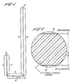
- a piece of flexible circuit board measuring 12.5 cm x 2.5 cm x 0.18 mm with 37 micrometres of copper laminated to each side was bent twice at right angles at 8 cm and 10 cm along the longest dimension to form a "J" as shown in Figure 1.
- the substrate was then used as the cathode and positioned in the cell such that the stem of the "J" (between points 1 and 2) was 2.5 cm from the anode and the hook of the "J" (between points 2 and 3) was pointing away from the anode.
- the electrophoretic coating was carried out at 100V for 30 seconds at 35°C. the thickness at each horizontal and vertical side (as shown in Figure 1) was measured. The results are recorded in the table below.
Abstract
Description
- This invention is concerned with photosensitive polymer compositions and their use in electrophoretic deposition processes, for example, to deposit on a conductive surface a uniform, negative-acting, aqueous-developable photoresist film that is resistant to strong inorganic acids and aqueous bases.
- Photoresists are photosensitive films capable of transferring an image onto a conductive surface, for example, the metal surface of a printed circuit board or lithographic plate. Liquid-type photoresists typically contain a combination of a film-forming resin or polymer and a photosensitive compound or photoinitiator dissolved or suspended in a solvent such as an organic liquid.
- Liquid-type photoresists can be negative-acting or positive-acting systems. In the case of a negative-acting photoresist or negative resist, after the film is deposited on a surface and the solvent is removed, e.g. by heating, the film is selectively exposed, typically through a photomask, to a source of energy, such as ultraviolet light. The photomask has areas that are opaque and other areas that are transparent to the exposing radiation. The pattern on the photomask formed by the opaque and transparent areas defines the desired image, for example, a circuit, which is to be transferred to the substrate surface. The exposed portions of a negative resist film become less soluble in a developing solution than the unexposed portions, as the result of a photochemical reaction between the photoinitiator and the polymer or resin upon exposure. This difference in solubility allows for the selective removal of the unexposed film and the transfer of the image to the surface. In a positive resist, the exposed portions of the film become more soluble than the unexposed portions in the developer, as a result of the photochemical reaction, allowing for the selective removal of the exposed areas. After either type of resist film is developed, the portions of the surface that are not protected by the resist may be etched, such as by the action of an oxidizing solution typically containing an inorganic acid. The remaining resist film may then be stripped from the surface leaving only the desired etched image on the substrate. Alternatively, a metallic substrate surface containing the imaged resist can be plated with a metal or combination of metals, for example, tin and lead. The resist may then be stripped and the exposed substrate metal may be etched to form the desired pattern or a circuit on the substrate surface. The historical background, types and operation of conventional photoresists is described in Photoresist Materials and Processes, W.S. DeForest, McGraw-Hill, 1975.
- Although liquid-type resists have been used for many years in lithographic and electronics applications, and despite numerous improvements to the resist systems and processing steps involved with their use, these conventional liquid resists still suffer from one or more disadvantages. For example, special surface preparations may be required to obtain good adhesion of a liquid resist film onto a surface. This increases the processing time and cost involved. The resists themselves may also require other special processing steps, such as hardening or baking steps, which also increase processing time. The cost of the resist components utilized in conventional systems, combined with the loss of materials in depositing a film and the difficulty in reproducibly synthesizing stable systems, has also been a problem. The most widely recognized drawback of liquid resists, however, has been the difficulty of depositing, on surfaces, films of uniform and adequate thickness whilst avoiding the formation of voids or pinholes. Furthermore, there remains a need for resists which have resistance to etching and electroplating baths and which are functional over a wide range of exposing radiations at minimal exposure doses and times. The use of organic solvents to formulate and develop liquid resists also presents a potential health, flammability and environmental concern, as well as adding to the potential for swelling the images formed and reducing the image resolution achievable.
- Despite the abundance of conventional liquid type photosensitive coatings, dry film type resists are also important in the preparation of printed circuit boards. Dry film resists are multilayer films in which the photoresist is precast into a solid film and sandwiched between a polyethylene film and a polyester cover sheet. Dry film resists are described in U.S. Patent Nos. 3,469,982, 4,378,264 and 4,343,885. The lamination, onto the surface of a printed circuit board, of the photoresist layer of a dry film resist is typically achieved by peeling away the polyethylene film layer from the adjacent photoresist layer and then bringing the thus exposed surface of the photoresist layer of the resulting photoresist layer/cover sheet combination into contact with the surface of the printed circuit board onto which the photoresist layer is to be laminated. The photoresist layer/cover sheet combination is then laminated onto the printed circuit board, for example, using hot rollers. The transparent cover sheet, which provides mechanical support for the photoresist film layer, is usually kept in place until after the photoresist is exposed through a photomask and the cover sheet. After exposure, the cover sheet is peeled away from the resist film and the resist is developed and processed in a conventional manner.
- Despite the advantages of these dry film resists over liquid-type resists, such as the ability to apply a uniformly thick coating without pinholes, dry film resists also suffer from a number of drawbacks. Typically, the conductive copper surface of a printed circuit board contains a protective coating, known as a chromate conversion coating, that protects the copper from oxidation. Therefore, before a dry film resist can be applied to the metal surface, the conversion coating must be removed, for example, by abrasive scrubbing. This scrubbing roughens the surface and facilitates adhesion of the dry film resist to the substrate surface. However, the use of an abrasive scrubber can lead to defective circuitry on subsequent etching operations. Dry film resists may also have difficulty in adhering to metal surfaces unless the metal has been specially prepared. In addition, dry film resists typically cannot be used effectively with surfaces having irregular topographies. For example, a small scratch in the substrate surface may not be filled by a dry film resist. The dry film may merely bridge the scratch and can allow etchant to seep into the scratch during etching resulting in unacceptable circuits. Furthermore, in addition to the high cost of dry film resists, their use also results in substantial waste of materials in the form of unusable strips of excess film because the dry film resists are typically trimmed to conform with the substrate surface to be coated.
- Electrophoresis refers to the motion of charged particles or molecules through a liquid medium under the influence of an applied electrical field. Electrophoretic deposition or electrodeposition is conducted in an electrolytic cell where the surface of the conductive material, to be coated by the migrating charged particles, serves as one electrode. Polymers bearing a positive charge in the liquid medium, or polymers which become associated with a substance such as a surfactant having a positive charge, are known as cationic polymers. The electrodeposition of cationic polymers on the surface of a negatively charged electrode (cathode) is referred to as cataphoresis, while the electrophoretic deposition of negatively charged polymers (anionic polymers) onto the surface of a positively charged electrode (anode) is known as anaphoresis.
- Coating metal objects with organic materials by electrophoresis is well known and is widely used to paint metal surfaces such as automobiles. Electrophoresis has been used to prepare electrical components, such as resistors and capacitors, that are integral to printed circuit boards (U.S. Patent No. 3,303,078). U.S. Patent No. 3,403,088 is directed to anaphoresis of water-dispersed acrylic interpolymers to prepare thermally curable, non-photoactive, insulating coatings for electrical devices. U.S. Patent No. 3,446,723 is also directed to thermally cured, non-photoactive, coatings preferably applied by cataphoresis. Cataphoresis is taught in U.S. Patent No. 3,446,723 to be superior to anaphoresis because nascent oxygen does not react with the polymers. In addition, metal ions are eliminated from passing into solution resulting in a decrease in the water repellancy and discoloration of the coatings. Other patents disclosing the use of electrophoresis to deposit non-photoactive, thermally-curable coatings include: U.S. Patents Nos. 3,925,181; 3,975,251; 3,200,057; 4,238,385; and 4,338,235. Polymer Compositions for Cationic Electrodepositable Coatings, P.E. Kondomenos and J.D. Nordstrom, Journal of Coatings Technology, Volume 54, No. 686, March 1982, pages 33-41 also describes recent advances in this coating area.
- Electrophoretic deposition of photosensitive coatings is also generally known. U.S. Patent No. 3,738,835 describes the use of anaphoresis to deposit a photosensitive composition from an emulsion prepared from a solution containing a polychloroprene polymer, a photosensitizer, such as 4,4'-bis-(dimethyl-amino)-benzophenone, a stabilizer, such as hydroquinone that prevents the unsaturated polymer from decomposing in solution, and a hardener such as a partially cured resin or other polymer to provide etch resistance, in an 80% butyl acetate/20% methyl ethyl ketone or 80% cyclohexanone/20% methyl ethyl ketone solvent, the percentages being percentages by volume. The emulsion is formed by the addition, to this solution, of an aqueous solution containing a wetting agent, such as a fluorocarbon anionic surfactant, N-methyl-2-pyrolidone and triethyl amine. Upon exposure of the photosensitive composition to radiation, the unsaturated polymer crosslinks and the unexposed film is developed with an organic solvent. U.S. Patents Nos. 3,954,587; 4,029,561; 4,035,273; 4,035,274; 4,039,414; 4,066,523; 4,070,258; and 4,166,017 also disclose coatings that are applied by electrophoresis and are cured by exposure to ultraviolet (UV) light and/or heat. These coatings are intended to provide a permanent protective coating or to improve the appearance of the article to be coated. These patents do not disclose or suggest that such coatings are useful as photoresists and, in fact, they are not suitable for such use. U.S. Patent No. 3,844,919 relates to the electrodeposition of a permanent photoconductive material prepared from a photoconductive zinc oxide, an electrically insulating resin, such as an acrylic resin, and an organic solvent or water.
- U.S. Patent No. 4,414,311 describes the preparation of lithographic printing plates by cataphoretically applying a thin, submicrometre photosensitive film, from an aqueous solution of a polymeric material having pendant diazonium salts, onto an electrochemically hydrophilized metal surface. The thin film is exposed to UV radiation, developed and inked to form a lithographic printing plate.
- Japanese patent application 77-11601 describes electrophoretically depositing a photosensitive polymer composition onto a silicate coated metal surface. The photosensitive polymers are soluble or dispersible in an aqueous medium and capable of being anaphoretically deposited on a conductive surface by virtue of containing neutralized acid groups. The polymers are photosensitive by virtue of containing unsaturated groups that crosslink upon exposure to light. The preparation of these polymers requires at least two steps; the first step being the preparation of a polymer having unsaturated groups or acid groups and the second step being either the addition of an acid to a polymer having unsaturated groups or the addition of unsaturated groups to a polymer having acid groups. This Japanese patent application illustrates the formation of such polymers from an acrylic polymer having acid groups and pendant hydroxy groups and an isocyanate-containing methacrylate compound. The preparation of these photosensitive polymers is difficult because of the number of separate reactions needed. In addition, the extent to which such polymers can be effectively crosslinked is limited by the number of available unsaturated groups on the polymer or the number of unsaturated groups that can be attached thereto. The number of unsaturated groups that can be attached to the polymer may also affect other desirable properties of the resist such as its aqueous solubility and capability to form high quality films. In addition, photosensitive compositions containing a neutralized acid group are not capable of being used in a cataphoretic deposition process and while the patent mentions cataphoresis, it fails to suggest any composition that can be used to cataphoretically form an aqueous acid- developable and strippable resist that is resistant to aqueous base solutions and inorganic acids.
- Japanese patent disclosure 55(1980)-148491 entitled Method for Preparing Printed Wiring Boards discloses using electrophoresis for coating photosensitive substances onto the copper surface of a copper-laminated plate in preparing printed circuit boards. However, this reference does not describe any materials useful for the process or any of the process conditions used therein.
- The present invention may enable the provision of photosensitive polymer compositions which are capable of being electrophoretically deposited from an aqueous solution or emulsion directly onto a conductive surface, for example as a uniform, adherent, photosensitive film of desired thickness, and which may solve the problems of conventional liquid-type and dry film resists. For example, the photosensitive polymer compositions may be electrophoretically deposited as a uniform film of desired thickness on a conductive surface of regular or irregular surface topography without the need for elaborate and time consuming surface preparation steps and without wastage of the photosensitive composition.
- The present invention may also enable the provision of photosensitive polymer compositions that can be cataphoretically deposited on a conductive surface as aqueous base and inorganic acid resistant films that can be developed with organic acids to form highly resolved images.
- According to the present invention there is provided a crosslinkable photosensitive polymer composition, which comprises (a) photoinitiator, and (b) at least one polymer having one or more carrier groups per polymer molecule, and wherein the composition contains unsaturated groups so that it is capable, upon exposure to actinic radiation, of forming a film containing crosslinked polymer.
- The photosensitive polymer compositions of the present invention are useful in electrophoretic deposition processes, for example, the electrophoretic deposition of a uniform photosensitive film of desired thickness on a conductive substrate, and in such use are conveniently used in the form of aqueous emulsions or solutions.
- One embodiment of the invention relates to a process for forming an aqueous inorganic acid and base resistant image on the surface is provided.
- A further embodiment of the invention is directed to cataphoretically deposited, aqueous-developable, negative photoresist films formed from the photosensitive polymer compositions containing at least one polymer having one or more positively charged carrier groups per polymer molecule, photoinitiator and unsaturated multifunctional crosslinking monomer.
- The photosensitive polymer compositions of the present invention, and deposited photosensitive polymer films formed therefrom, are capable of being crosslinked when the photoinitiator is activated by exposure to actinic radiation. This crosslinking reaction requires the presence, in the photosensitive polymer composition, of material containing unsaturation.
- The material containing unsaturation is preferably at least one unsaturated crosslinker monomer. The incorporation of unsaturated crosslinker monomer having two or more unsaturated groups in the photosensitive polymer composition, referred to herein as a multifunctional monomer, is preferred in the practice of the invention.
- Alternatively, the material containing unsaturation can be one or more polymers present in the photosensitive polymer composition. Such polymer(s) can be the polymer(s) containing one or more carrier groups per polymer molecule.
- Preferably, the photosensitive polymer composition is in the form of an aqueous solution or emulsion containing at least one polymer having one or more cationic carrier groups per molecule, photoinitiator, and unsaturated crosslinker monomer.
- Carrier groups are positively or negatively charged groups or groups capable of being positively or negatively charged upon reaction with an acid or base, respectively.
- By selection of a suitable monomer or mixture of monomers, it is possible to prepare a polymer or polymer mixture having a number of desirable properties for use in the photosensitive polymer compositions of the invention. Conveniently, the polymer or polymer mixture is capable of being deposited, from a low viscosity aqueous emulsion or solution, by electrophoresis, as a uniform, adherent film on a conductive surface. At least one polymer, in the photosensitive polymer composition, has one or more carrier group per polymer molecule, the number of carrier groups typically being sufficient to enable the polymer(s) to be useful in an electrophoretic process. The carrier group(s) is/are conveniently selected so that, after electrophoretic deposition of a film of the photosensitive polymer composition and subsequent exposure of a portion of the film to actinic radiation, the unexposed portion of the film can be easily removed using an aqueous acid or aqueous base developer depending on the charge of the carrier group(s). Typically, the polymer or polymer mixture is soluble in water to form a solution thereof, or possesses limited solubility in water to form an aqueous emulsion suitable for use in electrophoresis. Whilst photosensitive polymer compositions containing polymer(s) in the form of a solution can be used, in accordance with the present invention, in electrophoretic processes, it is preferred to use photosensitive polymer compositions containing polymer(s) in the form of aqueous emulsions in such processes.
- Photosensitive polymer compositions according to the present invention can be used with conventional film forming techniques, other than electrodeposition, to form films, for example photoresists, having the same desirable properties as films formed from aqueous solutions or dispersions of the photosensitive polymer compositions by electrodeposition onto conductive substrates.
- Typically, when a polymer film is deposited, from an aqueous solution or emulsion of a photosensitive polymer composition according to the present invention, preferably by cataphoresis, and crosslinked by exposure to actinic radiation, the crosslinked film is essentially insoluble in aqueous acids and resistant to etchants, such as those containing inorganic acids, and electroplating baths. At the same time the portions of the film that are not exposed to actinic radiation are typically soluble in, or easily removable by, aqueous organic acids.
- The polymer(s) having one or more carrier groups per polymer molecule may, for example, have a molecular weight of from about 10,000 to about 100,000 and a glas transition temperature of from about 0°C to about 100°C.
- Suitable polymers for use in the photosensitive polymer compositions of the invention include addition or condensation polymers having one or more carrier groups per polymer molecule. Addition polymers having one or more carrier groups per polymer molecule, prepared from monomers having ethylenic unsaturation, are preferred. Polymers containing one or more carrier groups per polymer molecule that are useful in the photosensitive polymer composition include acrylic polymers, vinyl polymers other than acrylic polymers, epoxy polymers, polyurethanes, polyesters and polyamides. Positively charged carrier groups, or cataphoretic carrier groups, include, for example, quaternary ammonium groups, sulfonium groups and sulfoxonium groups.
- Other groups which become positively charged upon reaction with an acid, for example amine groups, may also be employed. The acids that are useful to protonate the carrier group(s) of the polymer(s) include lactic acid, glycolic acid, hydroxyacetic acid, hydrochloric acid, formic acid, acetic acid and phosphoric acid.
- Negatively charged carrier groups, or anaphoretic carrier groups, include, for example, carboxylic acid groups.
- Acrylic polymers containing one or more carrier groups per polymer molecule can be prepared by the polymerization or copolymerization of acrylic acid, methacrylic acid, the esters of amides thereof, or mixtures of such monomers, provided that at least one such monomer contains one or more carrier group. For example, the composition of the invention may comprise polymer formed from a mixture of monomers containing from 8 to 15 weight percent acrylic or methacrylic acid. An acrylic polymer bearing one or more cataphoretic carrier groups can be prepared by the polymerization of monomers, one of which has a basic amine group, such as 2-(dimethylamino)ethyl methacrylate (DMAEMA), or 3-(dimethylamino) propyl methacrylamide (DMAPMA). The amine groups on the polymer can be converted to positively charged amine salts by reaction with an acid, for example, lactic acid. Similarly, (meth)acrylic acid polymers bearing one or more anaphoretic carrier groups may be prepared from acrylic acid or methacrylic acid monomers alone or with other monomers such as lower alkyl acrylic or methacrylic acid esters where the alkyl group contains from 1 to about 8 carbon atoms, for example methyl methacrylate or butylacrylate. The pendant carboxylic acids on the poly(meth)acrylic acid polymers can then be converted to the negatively charged carboxylate salts by reaction with a base, for example, sodium hydroxide.
- Alternatively, it is also possible to modify polymers having no carrier groups to incorporate one or more such carrier groups. For example, a glycidyl methacrylate polymer can be reacted with an amine to attach one or more amine carrier groups to the polymer chain.
- Vinyl polymers, other than the acrylic or methacrylic polymers described above, incorporating one or more carrier groups may also be used. These polymers may be prepared by the polymerization of vinyl monomer(s), for example, styrene, substituted styrene, vinyl halides such as vinyl chloride, vinyl esters such as vinyl acetate, and/or vinyl ethers such as methyl vinyl ether, alone or with other vinyl monomer(s) containing one or more carrier groups such as 2-methylvinylimidazole and vinyl imidazole containing cataphoretic carrier groups.
- It is also possible to prepare polymers that are suitable for the practice of this invention from the polymerization of the acrylic and/or methacrylic monomers together with the vinyl monomers other than acrylic and methacrylic monomers, provided that at least one of the monomers contains one or more carrier group.
- Epoxy polymers are also useful in the photosensitive polymer compositions. They are typically prepared by the reaction of di-epoxides with diols, diamines or dicarboxylic acids. The polymerization of a di-epoxide with a diol can be carried out in the presence of an amine to incorporate one or more cataphoretic carrier groups into the polymer. Anaphoretic epoxy polymers can be prepared from uncharged epoxy polymers by chemical reactions that attach one or more carboxylic acid carrier groups to the epoxy polymers.
- Polyurethanes which can be used in the photosensitive polymer compositions are typically prepared by the reaction of diisocyanates with diols. Residual isocyanate groups can be reacted with hydroxyamines, such as triethanolamine, to attach one or more amine carrier group for cataphoretic deposition. Anaphoretic polyurethane polymers can be prepared by reacting residual hydroxyl groups with anhydrides of polycarboxylic acids, such as trimellitic anhydride, to attach one or more acid carrier groups.
- Polyesters with terminal carboxylic acid groups are suitable anaphoretic polymers for use in the photosensitive polymer composition. These polymers can be converted to cataphoretic polymers by reaction with primary 2-aminoalcohols, such as 2,2-di(hydroxymethyl)-2-aminoethanol, to form one or more oxazoline carrier groups.
- A preferred class of polymers suitable for cataphoresis are prepared by the free radical polymerization in a suitable solvent of esters and/or amides of acrylic acid and/or methacrylic acid, where at least one of the monomers contains one or more amine carrier groups. Suitable solvents for the polymerization include the monopropyl ethers of 1,2-propanediol (such as Propasol-P manufactured by Union Carbide Corporation), methyl cellosolve, ethyl cellosolve, butyl cellosolve, cellosolve acetate, methyl carbitol, butyl carbitol, 1,2-dimethoxyethane, diethylene glycol dimethyl ether, isopropanol, propanol, n-butanol, sec-butanol, isobutanol, ethylene glycol, 1,3-propanediol, acetone, methyl ethyl ketone, methyl isobutyl ketone, tetrahydrofuran, ethyl acetate, butyl acetate, 1,4-dioxane, toluene, xylene, acetonitrile, dimethylformamide and dimethylsulfoxide. Solvents that are very soluble in water are preferred.
- The polymer cr polymer mixture containing one or more carrier groups per polymer molecule conveniently contains from at least about 10 milliequivalents of charged carrier group per 100 grams of the polymer or polymer mixture (in order for the polymer or polymer mixture to be water- dispersible and capable of being electrophoretically depositable as a film) to less than about 200 milliequivalents of charged carrier group per 100 grams of polymer or mixture (in order for the electrophoretically deposited film to be capable of being selectively developed without adversely affecting the exposed areas of the film). The milliequivalents of charged carrier group per 100 grams of polymer (meq/100 g) is calculated based on the assumption that each equivalent of acid (in the case of a cataphoretic carrier group) added has protonated each group, such as an amine, on the polymer.
- In the case of the cataphoretic polymers containing one or more positively charged carrier groups per polymer molecule, it is preferred that the polymer contain from about 20 to about 100 meq/100 g. Even more preferred are cataphoretic polymers containing from about 25 to about 75 meq/100 g.
- The molecular weight of the polymers used in the photosensitive polymer composition of the invention is conveniently less than 100,000 weight average molecular weight. When acrylic, methacrylic, or the other vinyl polymers containing one or more carrier groups per polymer molecule are used, the weight average molecular weight conveniently ranges from about 10,000 to about 100,000, and preferably from about 20,000 to about 60,000 weight average molecular weight.
- One particularly preferred cataphoretic polymer mixture useful in the photosensitive polymer composition of the invention is formed from about 2 to about 15 weight percent DMAEMA, about 2 to about 43 weight percent ethyl acrylate, and from about 83 to about 55 weight percent methyl methacrylate, the percentages being based on the total weight of DMAEMA, ethyl acrylate and methyl methacrylate. These copolymers have a molecular weight of from about 10,000 to about 100,000 and a glass transition temperature of from about 0°C to about 100°C. When this polymer mixture is formulated as an aqueous emulsion with crosslinking unsaturated monomer, photoinitiator and acid, to protonate the carrier groups, the cataphoretically deposited adherent film formed on a conductive substrate surface is readily developed with an aqueous solution of an organic acid and the exposed areas of the film are resistant to strong inorganic acid solutions and strong aqueous bases.
- Preferred photosensitive polymer compositions of the invention are formed by mixing the polymer(s) containing one or more carrier groups per polymer molecule with at least one unsaturated monomer so that the photosensitive polymer films formed from the photosensitive polymer compositions are capable of being polymerized into crosslinked polymers by photoinitiator when exposed to actinic radiation. Unsaturated monomers having two or more unsaturated groups attached to the same molecule, referred herein as multifunctional monomers, are preferred. More preferred are multifunctional monomers having two or more acrylate or methacrylate groups attached to each monomer molecule. The multifunctional monomer, when used, is usually added to the polymer or polymer mixture so that there is sufficient unsaturation to give a Bromine Number of about 35 or greater. A Bromine Number is a generally accepted method used to determine the degree of unsaturation in a sample. The Bromine Number refers to the number of grams of bromine needed to react with all the unsaturated groups in 100 grams of a sample.
- Examples of suitable multifunctional monomers include the following: allyl methacrylate; 1,4-benzenediol diacrylate; 1,4-benzenediol dimethacrylate; bis-(acryloxy- ethyl)phosphate; bisphenol-A diacrylate; bisphenol-A dimethacrylate; 1,3-butanediol diacrylate; 1,3-butanediol dimethacrylate; 1,4-butanediol diacrylate; 1,4-butanediol dimethacrylate; 2-butene-l,4-diol diacrylate; 2-butene-1,4-diol dimethacrylate; butylene glycol dimethacrylate; 1,2,4-butanetriol trimethacrylate; crotyl acrylate; crotyl methacrylate; 1,4-cyclohexanediol diacrylate; 1,4-cyclohexanediol dimethacrylate; decamethylene glycol diacrylate; decamethylene glycol dimethacrylate; diallyl isocyanurate; diallyl itaconate; diethylene glycol diacrylate; diethylene glycol dimethacrylate; di-(3-acryloxyethyl) ether of bisphenol-A; di-(3-acryloxy-2-hydroxypropyl) ether of bisphenol-A; diallyl fumarate; diisopropenylbenzene; di-(3-methacryloxyethyl) ether of bisphenol-A; di-(3-methacryloxy-2-hydroxypropyl) ether of bisphenol-A; di-(3-methacryloxy-2-hydroxypropyl) ether of tetrachlorobisphenol-A; di-(3-methacryloxy-2-hydroxypropyl) ether of tetrabromobisphenol-A; di-(3-methacryloxy-2-hydroxypropyl) ether of 1,4-butanediol; di-(3-methacryloxy-2-hydroxypropyl) ether of diphenolic acid; 2,2-dimethyl-1,3-propanediol diacrylate; 2,2-dimethyl-1,3-propanediol dimethacrylate; dipropylene glycol dimethacrylate; ethylene glycol diacrylate; ethylene glycol dimethacrylate; gycerol triacrylate; gycerol trimethacrylate; hexamethylene glycol diacrylate; hexamethylene glycol dimethacrylate; hydrogenated bisphenol-A dimethacrylate; melamine acrylate; methallyl ethacrylate; N,N'-methylenebisacrylamide; 1,9-nonanediol dimethacrylate; 1,5-pentanediol diacrylate; 1,5-pentanediol dimethacrylate; pentaerythritol tetraacrylate; pentaerythritol tetramethacrylate; pentaerythritol triacrylate; pentaerythritol trimethacrylate; 1-phenyl-1,2-ethanediol dimethacrylate; polyoxyethyl-2,2-di(p-hydroxyphenyl)propane diacrylate; polyoxyethyl-2,2-di(p-hydroxyphenyl)propane dimethacrylate; polyoxypropyltrimethylolpropane triacrylate; 1,3-propanediol diacrylate; 1,2-propanediol dimethacrylate; 1,3-propanediol dimethacrylate; propoxylated bisphenol-A dimethacrylate; tetraethylene glycol diacrylate; tetraethylene glycol dimethacrylate; 1,3,5-triacryloylhexa- hydro-s-triazine; triethylene glycol diacrylate; triethylene glycol dimethacrylate; 1,3,5-isopropenyl- benzene; trimethylolethane triacrylate; trimethylolpropane diallyl ether mono-methacrylate; trimethylolpropane triacrylate; trimethylolpropane trimethacrylate; 2,2,4-trimethyl-1,3-pentanediol dimethacrylate; tripropylene glycol diacrylate; tris-(2-acryloxyethyl) isocyanurate; and tris-(2-methacryloxyethyl) isocyanurate. Also useful are the acrylate and methacrylate esters of polyalkoxylated compounds such as those described in US Patents Nos: 3,594,410; 4,180,474; and 4,382,135; polyoxyethylated trimethylolpropane triacrylate and trimethacrylate and similar compounds as disclosed in U.S. Patent No. 3,380,831; and the esters of 2-acryloxypropionic acid such as those prepared by the Michael addition of acrylic acids as described in EP-A-0081973.
- Preferred unsaturated crosslinker monomers are those where at least one, and preferably most, of such unsaturated linkages are conjugated with a double bonded carbon, for example, carbon double bonded to carbon or to such heteroatoms as nitrogen, oxygen and sulfur. The most preferred crosslinker monomers are those where the ethylenically unsaturated groups are conjugated with esters or amides, such as pentaerythritol triacrylate.
- The photosensitive polymeric composition contains photoinitiator. A photoinitiator is a material that will polymerize the unsaturated group(s), present, for example, in the polymer(s) and/or unsaturated crosslinker monomer(s), when exposed to radiation of an appropriate wavelength. Examples of photoinitiators suitable for use in the polymeric composition include the azo compounds, sulfur containing compounds, metallic salts and complexes, oximes, amines, polynuclear compounds, organic carbonyl compounds and mixtures thereof as described in U.S. Patent No. 4,343,885, column 13, line 26 to column 17, line 18; and 9,10-anthraquinone; 1-chloroanthraquinone; 2-chloroanthraquinone; 2-methylanthraquinone; 2-ethylanthraquinone; 2-tert-butylanthraquinone; octamethylanthraquinone; 1,4-naphthoquinone; 9,10-phenanthrenequinone; 1,2-benzanthraquinone; 2,3-benzanthraquinone; 2-methyl-1,4-naphthoquinone; 2,3-dichloronaphthoquinone; 1,4-dimethylanthraquinone; 2,3-dimethylanthraquinone; 2-phenylanthraquinone; 2,3-diphenylanthraquinone; 3-chloro-2-methylanthraquinone; retenequinone; 7,8,9,10-tetrahydronaphthalenequinone; and 1,2,3,4-tetrahydrobenz(a)anthracene-7,12-dione. Other photoinitiators which are also useful are described in U.S. Patent No. 2,760,863 and include vicinal ketaldonyl alcohols, such as benzoin, pivaloin, acyloin ethers, e.g., benzoin methyl and ethyl ethers; alpha-hydrocarbon- substituted aromatic acyloins, including alpha-methylbenzoin, alpha-allylbenzoin, and alpha-phenylbenzoin. Photoreducible dyes and reducing agents disclosed in U.S. Patent Nos: 2,850,445; 2,875,047; 3,097,096; 3,074,974; 3,097,097; and 3,145,104 as well as dyes of the phenazine, oxazine and quinone classes, benzophenone, 2,4,5-triphenyl- imidazolyl dimers with hydrogen donors, and mixtures thereof as described in U.S. Patent Nos. 3,427,161; 3,479,185; and 3,549,367 can be also used as photoinitiators. Also useful with photoinitiators are sensitizers as disclosed in U.S. Patent No. 4,162,162.
- The photoinitiators which have been found to be preferred for use in the photosensitive polymer compositions of the invention include: 3-phenyl-5-isoxazolone/ benzathrone; 2-t-butylanthraquinone; 2,2-dimethoxy-2-phenylacetophenone; 1-hydroxycyclohexyl phenyl ketone, and diethoxyacetophenone. Other suitable photoinitiators are disclosed in Nippon Kagaku Kaisha No. 1192-199 (1984) and include 2,4,6-tris (trichloromethyl)-1,3,5-triazine with 3,3'-carbonyl bis (7-diethylaminocoumarin), 1-methyl-2-benzylmethylene-1,2-dihydronaphthol (1,2d) thiazole, or 9-phenylacridine; 2-mecaptobenzimidazole with 9-phenylacridine; and 3-phenyl-5-isoxazoline with 9-fluorenone or 1-methyl-2-benzylmethylene-1,2-dihydronaphtho (1,2d) thiazole.
- Preferred photosensitive cataphoretic polymeric compositions of the invention are conveniently formed by mixing a solution of the polymer(s) with unsaturated crosslinker monomer. The photoinitiator, dissolved in a suitable solvent, is then added with stirring to this solution and the acid, used to protonate the carrier groups, is added to the stirred mixture. After the mixture is completely mixed, water is added. As the water is added, the mixture becomes less viscous and an aqueous emulsion is formed. The solids content of the emulsion can be adjusted by diluting the emulsion with additional water. Typical relative concentrations of polymer, photoinitiator, unsaturated monomer and acid are illustrated in Table 1 where all components are expressed on a weight basis, based on 100 parts by weight of the polymer.

- The process of cataphoretically depositing a photosensitive polymeric film from an aqueous solution or emulsion can be accomplished using the following procedure. A substrate having a conductive surface, such as a circuit board material having copper cladding on each side, may be scrubbed with an abrasive cleaner, dried with air and lowered into the aqueous emulsion or solution to serve as the cathode. Preparing the substrate by scrubbing with an abrasive cleaner is not necessary to obtain good adhesion of the photosensitive film and can be eliminated from the process if desired. An inert counter electrode, such as stainless steel, is used as the anode. The anode is also submerged into the aqueous emulsion or solution such that the two electrodes are parallel to each other and separated by a fixed distance of at least about 0.5 centimetres. The electrodes are connected to a constant voltage, direct current power supply. A potential on the order of one hundred volts is then applied. The amount of applied voltage and the time that the voltage is applied determines the thickness of the deposited film. The time that the voltage is applied should be less than about one minute, and preferably as short as from about 5 to 15 seconds. A decrease in the current, as monitored on a strip chart recorder during the time the voltage is applied, to about 10 to 15 percent of the initial current level indicates complete electrodeposition. The power source is then disconnected and the cathode is removed from the aqueous emulsion or solution, rinsed with water and dried with air or nitrogen. The film can optionally be baked at about 100°C for about 10 minutes to reduce tack and increase abrasion resistance of the film if desired. The thickness of the deposited film or coating may be measured, for example by using an Alpha Step profiler manufactured by Tencor Instruments. The profiler measures the thickness of the film as follows: A small section of the film is scraped away from the substrate and the sample is positioned in the profiler so that the stylus of the profiler is drawn along the copper cladding on the substrate surface and from the substrate surface onto the surface of the deposited film. The profiler monitors the distance that the stylus travels as it climbs from the surface of the copper cladding to the surface of the film. This distance is equal to the thickness of the deposited film.
- This procedure is also suitable for anaphoretic deposition using the anaphoretic photosensitive polymer composition of the invention using the conductive surface as the anode and the inert counter electrode as the cathode.
- During cataphoretic electrodeposition from an aqueous solution or emulsion, the polymer(s) containing the positively charged carrier group(s) migrate toward the cathode surface while water is being electrolyzed at the cathode forming hydrogen and hydroxide ions. Due to hydroxide formation, the pH at the cathode surface is much higher than in the bulk of the solution or emulsion. When the polymer particles reach the cathode surface, the positively charged carrier groups, such as the protonated amine groups of the polymer, react with the hydroxide ions to form water and neutral carrier groups, such as neutral amine groups, on the polymer. These unprotonated carrier groups are not capable of stabilizing polymer particles in the emulsion or the solution and the polymer particles precipitate onto the cathode surface, coalescing with other like particles and forming a film on the cathode surface. The film acts as an electrical insulator for the cathode, and as the film grows in thickness the resistance between the two electrodes increases and the current drops. This drop in current reduces the deposition rate for additional film until the growth of the film eventually stops. Therefore, when the initial current is reduced to about 10 to 15 percent of its initial level effectively complete electrodeposition has occurred. The growth of the film is therefore self-limiting and typically results in an even, uniformly thick coating or film over the entire conductive substrate surface.
- The photosensitive film-coated substrate can then be exposed and developed to transfer an image, such as a pattern delineated on a photomask, onto the substrate. Exposure of the film can be carried out at atmospheric pressure (air) by placing the photomask in contact with the film and exposing the film, through the mask, to the desired radiation, e.g. light. Exposure of the film is preferably carried out under partial vacuum by placing the film coated substrate and photomask in a frame that is capable of sustaining at least a partial vacuum and which has a window that is transparent to the exposing radiation. When the vacuum is applied, the seal that the window rests on is compressed so that the window presses the mask firmly onto the photosensitive film. The exposing radiation, such as unfiltered ultraviolet light produced by a mercury lamp having an average wavelength of about 366 nanometres, can then be used to expose the photosensitive film through the photomask. The photomask used in the illustrative examples described hereinafter was a Stouffer Resolution Guide (1-T) made of a transparent film having an opaque pattern. Part of the pattern consists of ten black or opaque lines, in a side-by-side pattern, which are tapered so that the width of the lines ranges from a distance of about 5000 micrometres to about 10 micrometres. The space between the lines at any point is about 1.5 times the width of the lines at that point, for example, if the lines are 300 micrometres in width, the space between the lines is about 450 micrometres. Another part of the photomask has a negative image formed by transparent lines separated by opaque spaces on a pattern as described above. Calibration bars which cross the lines at several places serve to indicate the width of the lines.
- The power of the exposing radiation that reaches the film can be measured before the exposure of the film. A Hybrid Technologies Group Power Meter (Model 100) was used to measure the exposure power at about 366 nanometres. This meter uses a photocell with a filter that filters out wavelengths other than those of about 366 nanometres. The meter is placed under the exposure lamp at a position normally occupied by the sample to be exposed. The signal from the photocell is converted to a digital readout in power units (milliwatts per square centimetres). The power can then be converted to energy units (millijoules per square centimetre) by multiplying the power units by the exposure time (seconds).
- Following exposure and the removal of the photomask, the photosensitive film can be developed by subjecting the film to a developing solution either by spraying the developer onto the film or by immersing the film coated substrate into a developing solution. Developer solutions that have been found to be useful for developing cataphoretically deposited negative photoresist films of the invention include, for example, from about 10 to about 15 weight percent aqueous solutions of acetic, lactic, glycolic, formic or succinic acid, with acetic acid being the preferred developer. Conveniently, the developer solutions are used at temperatures ranging from about 20°C to about 50°C.
- During immersion development of cataphoretically deposited negative resists of the invention, the developing solution is typically stirred gently for a sufficient time to cause complete protonation of the amine or other carrier group(s) on the polymer in the unexposed areas making these film areas sufficiently hydrophillic and soluble in, or swellable by, warm water at temperatures of from about 45 to about 50°C so that the developed areas are easily removed from the surface.
- Spray development may, for example, be conducted by pumping the developer through a spray nozzle onto the surface of the exposed film coated substrate. The unexposed film is then removed by the sprayed developer. Excess developer may be removed from the surface by rinsing with water. Following development, the substrate surface can then be dried with air or nitrogen.
- The exposed, crosslinked, areas of the film are more resistant to the reaction with the developer and are much less soluble, even after some limited reaction with the developer, than the unexposed areas. During the time that is required to completely remove the unexposed portions of the film, the exposed areas remain essentially unaffected.
- The conductive surface of the substrate not covered by the exposed, crosslinked, resist film can be etched and removed using common oxidizing agents. For example, with a substrate having a copper metal surface, a solution of ferric chloride, cupric chloride or commercially available etchants such as Shipley Company Neutra-Etch V-1 (alkaline ammonia) or Hydroetch 536 can be used. Other etching solutions and etching techniques which are commonly used are described in The Printed Circuit Handbook, C.F. Coombs, Jr., pages 8-11 to 8-27.
- After etching, the photosensitive film may be stripped to reveal lines of unetched metal on the substrate. Stripping the photosensitive film may be carried out by immersing the exposed photosensitive film coated substrate in a stripping solution or by spraying the stripping solution on the resist, similar to the techniques described above in connection with the development step, until the exposed film is removed.
- Aqueous solutions which may be used to strip the resist are similar to those used to develop the resist. They can also contain minor amounts of surfactants and other additives. Suitable aqueous stripping solutions include 5 weight percent solutions of succinic acid, butyl carbitol or butyl cellosolve. These stripping solutions may be used at elevated temperatures, for example, about 50°C.
- The resolution of the developed photosensitive film or image on the surface is defined as the minimum width of lines and spaces, corresponding to the alternating opaque and transparent lines on the photomask, that are reliably transferred to the photosensitive film image after etching and stripping. Lines having a continuous surface of unetched metal on the surface are considered resolved. The resolution as actually reported is the nominal width of the line in the photomask used to produce that line although the actual width of the etched line may be slightly less due to slight undercutting of the exposed film by the etchant.
- The use of the photosensitive polymer composition to electrophoretically deposit an inorganic acid resistant, negative photoresist, which can be further processed as described generally above, is described in greater detail in the examples that follow.
- The photosensitive polymer composition of the invention can also be used as a photoresist for chemical milling and as a solder mask for printed circuit boards. In chemical milling, a metal workpiece that is to be milled can be electrophoretically coated with the photosensitive polymer composition. The areas of the coated workpiece which are desired to be protected during milling are exposed to ultraviolet light. The unexposed resist is then removed by a developer leaving bare metal areas. The bare metal areas of the workpiece are then etched with a solution that doesn't affect the photoresist.
- When the photosensitive polymer composition is used as a solder mask for printed circuit boards, the conductive lines of a finished printed circuit board are coated with the photosensitive polymer composition. The coating is exposed in all areas except where a component is to be soldered to the circuit. The unexposed film is developed to expose the bare metal portion of the conductive line where the solder is to be applied. During soldering, the solder will adhere to the bare metal but will not contact other areas of the conductive lines coated by the exposed film. The solder resist film thereby prevents shorts, caused by solder bridging the conductive lines, and protects the lines against corrosion and abrasion.
- The photosensitive resin can be used for the preparation of printing plates. The printing plate can be coated with the photoresist film, exposed through a mask with transparent areas corresponding to the areas to be coated with ink. The resist is developed to remove the unexposed resist. The plate bearing the resist image is inked with an ink that adheres to resist but not to the plate surface. The inked plate is pressed against the paper to transfer the ink to the surface of the paper. Alternatively, the plate bearing the resist image can be etched to partially remove areas not covered by the resist. The resist is then stripped and the plate is inked, coating the areas that were not partially removed by the etching. The plate is pressed against the paper to transfer the ink to the surface of the paper.
- In addition, the photosensitive composition can also be used advantageously to prepare screens for cathode ray tubes by electrophoretically coating the photosensitive polymer composition onto a conductive opaque surface. Cathode ray tube surfaces are normally not planar but curved, and obtaining a uniform photoresist coating on such a surface can be difficult to accomplish using conventional liquid resists. A photomask, having opaque areas corresponding to the areas that will be transparent in the final screen, is placed over the photosensitive film and the film is exposed and developed. The opaque surface not protected by the film is etched down to the transparent support and the screen is then processed in a conventional manner to make a cathode ray tube.
- The photosensitive polymeric composition of the invention can also be used with printed circuit boards formed by electroplating a dissimilar material, such as a tin/lead alloy, on the copper foil substrate not protected by the exposed photosensitive film. Following electroplating, the film is stripped to reveal the bare copper foil that is then etched using an etchant that doesn't attack the dissimilar electroplated metal image.
- Additional uses of the photosensitive polymer composition of the invention will be readily apparent from the following Examples, and the accompanying drawings referred to therein, the Examples being provided for illustrative purposes only and are not to be construed as imposing any limitation on the scope or applicability of the invention. All percentages used in the Examples are on a weight basis unless specifically stated otherwise.
- In the accompanying drawings:-
- Fig. 1 is a schematic drawing of a "J" shaped copper-laminated flexible circuit board used as a cathode in a cataphoretic process of the invention.
- Fig. 2 is a cross-sectional view of the circuit board illustrated in Fig. 1 taken at the point illustrated in Fig. 1.
- Four hundred grams of Propasol-P solvent was placed in a four neck round bottom flask fitted with a mechanical stirrer, nitrogen inlet tube, condenser and thermometer. Nitrogen gas was bubbled through the solvent and exhausted through an oil bubbler attached to the condenser to degas the solvent and flush the air from the reaction vessel. The nitrogen inlet tube was raised above the level of the solvent and a flow was maintained to keep a positive pressure of nitrogen in the flask throughout the reaction. A thermostatically controlled heating mantle was fitted to the underside of the flask and the solvent was heated to 105°C. A mixture of 48 grams of 2-(dimethylamino)ethyl methacrylate, 408 grams of methyl methacrylate and 162 grams of butyl acrylate and 6.2 grams of t-butyl peroctoate, a free radical initiator, was added dropwise over a four hour period to the stirred reaction vessel. An additional 0.6 grams of t-butyl peroctoate (10% of the originally added amount) was added to the reaction vessel 20 minutes after the addition of all the monomers. The heating and stirring was maintained for another 30 minutes and then discontinued. The polymer solution formed had a solids content of 61 weight percent indicating the essentially complete conversion of the monomers to polymer.
- An aqueous emulsion was then prepared by stirring 16.4 grams of the polymer solution with 5.0 grams of a multifunctional monomer, pentaerythritol triacrylate, 1.9 grams of a 21 weight percent solution of 2-t-butyl-anthraquinone photoinitiator in glyme (1,2-dimethoxyethane). To the above mixture was then added stepwise 0.2 millilitres of 85 weight percent aqueous lactic acid. Deionized water was then added slowly with stirring until the mixture was completely dispersed and until the viscosity of the mixture was noticeably reduced. Deionized water was added to make a total of 150 g of the photosensitive polymeric emulsion having a solids content of about 10 weight percent.
- A printed circuit board, having a thickness of 1.59 mm (one sixteenth inch), measuring 2.5 centimetres by 10 centimetres and having 305.17 g/m2 (one ounce per square foot) of copper clad to each side, was scrubbed with an abrasive cleaner (Shipley Company Scrub Cleaner 11), dried with a stream of air and lowered about 5 centimetres into the photosensitive polymeric emulsion prepared in Example 1. A stainless steel electrode of the same size as the printed circuit board was also submerged in this emulsion to form an electrolytic cell. The two electrodes were positioned parallel to each other separated by a distance of 2.5 centimetres. The electrodes were connected to a DC power supply, the stainless steel electrode being the anode and the circuit board surface being the cathode. An electrical potential of 100 volts was applied for 12 seconds. The temperature of the emulsion was 30°C and the initial current density was 15 milliamps per square centimetre. The power supply was then disconnected and the coated board was removed from the emulsion, rinsed with water and dried with nitrogen. The thickness of the coating was 5 micrometres as measured using the Alpha-Step Profiler.
- The film coated printed circuit board prepared in Example 2 was placed in a vacuum frame with a Stouffer Resolution Guide photomask and exposed with 1 mW/cm2 of unfiltered 366 nm ultraviolet light. The exposure time was 3 minutes and the exposure power as measured by a Hydrid Techologies Group Power meter (Model 100) was about 1 milliwatt per square centimetre.
- The exposed film was then developed by immersion in an aqueous solution of 15 weight percent acetic acid at 45°C with a constant back and forth motion of the substrate for two minutes. The substrate was then washed under a stream of warm (45°C) water for 10 to 15 seconds and dried with a stream of nitrogen.
- Lines and spaces of 25 micrometres in the Stouffer Resolution Guide were accurately reproduced in the imaged photoresist pattern.
- Printed circuit boards prepared according to Example 3 were then etched by submerging each board in one of the following inorganic etchants while stirring back and forth until the bare copper, not protected by the photoresist, was etched away revealing the insulating material of the board. The condition of the etched printed circuit board after etching with each etchant was visually inspected to determine if the photosensitive film was attacked by the etchant or if the film failed to adequately protect the copper, under the film, from the etchant. The results of the etching tests are shown in Table 1.

- 1) Ferric Chloride etchant was a 38 weight % solution having 1.402 specific gravity, 42 Baume, 530 g/L (4.45 lb/gal) density and 3.27 molarity at 20 to 25°C as described in the Printed Circuit Board Handbook, pages. 8-20, Table 8.5. Optimum FeC13 solution.
- 2) Cupric Chloride etchant was a CuCl2·2H2O at 2.2 M, 7.925 mL/litre (30 mL/gal) HC1 (20°C Be), 4M NaCl with water to make up 3.785 litres (1 gallon) as described in Printed Circuit Handbook, pages 8-15, Table 8.2-2.
- 3) Another developed photosensitizer film board was heated with a stream of air at temperature of 170°C for about 1 minute prior to etching with Shipley Hydro-Etch 536 to produce etched lines with 75 micrometre resolution. The finer lines of this pattern had less of a tendency to peel away from the copper substrate than the sample illustrated in Table 1 that had not been heated prior to Hydro-Etch 536.
- The Hydro-Etch 536 printed circuit board described in Example 4 (footnote 3) that had been heated prior to etching was placed in an aqueous stripping solution containing 15% acetic acid at 60°C for 8 minutes. The photosensitive film was softened and was easily brushed away from the surface leaving a clean copper surface.
- A printed circuit board containing the developed photosensitive polymer film of Example 3 was electroplated with solder in the areas not covered by the photosensitive film for 10 minutes at 10 milliamps per square centimetre to produce a layer of solder about 5 micrometres thick. The film was visually examined and found to be essentially unaffected by the plating process. No pinholes in the film which would have resulted in the formation of solder in undesired areas were found by inspection under 70X magnification.
- A standard copper plating bath and a standard solder plating bath were prepared according to the Printed Circuit Handbook, C.F. Coombs, Jr., pages 7-16 to 7-18 and 7-19 to 7-22, respectively. The resistance of exposed photosensitive polymeric film was tested by placing a printed circuit board, prepared according to Example 3, in the copper plating bath for 60 minutes and then in the solder plating bath for 30 minutes. The film was then inspected for any substantial change in hardness and adhesion or for signs of attack by the plating bath or changes in the image. The printed circuit boards remained essentially unchanged in the plating baths and no pinholes were detected by inspection under 70X magnification.
- A photosensitive polymer composition was prepared by formulating an aqueous emulsion using the same materials and procedures as in Examples 1 and 2 except that 4.0 grams of trimethylolpropane trimethacrylate was substituted for the pentaerythritol triacrylate multifunctional monomer. The aqueous emulsion was then cataphoretically deposited onto a printed circuit board. After 12 seconds at 100 volts and at 20°C, the coating thickness was measured to be 5 micrometres. The film coated board was exposed under vacuum using a Stouffer resolution guide and mercury lamp (UV 366 nanometres) for 3 minutes at an intensity of 1 milliwatt per square centimetre and developed with an aqueous solution of 15 weight percent acetic acid at 40°C for 2.5 minutes. Lines and spaces of 30 micrometres resolution were obtained in the photoresist image on the copper.
- Example 8 was repeated with the following modifications: 5.0 grams of trimethylolpropane triacrylate multifunctional monomer were used instead of 4.0 grams of trimethylolpropane trimethacrylate in preparing the photosensitive polymer composition. Cataphoretic deposition at 21°C for 12 seconds resulted in a film of 4 micrometres thickness. The film was exposed, under vacuum using the Stouffer resolution guide, to UV radiation (366 nanometres) for 3 minutes at 1 milliwatts per square centimetre. The unexposed film was developed for 3.5 minutes at 30°C in an aqueous solution of 15 percent acetic acid. Lines and spaces of 30 micrometres were resolved in the imaged photoresist image on the copper.
- Example 1 was repeated this time by using 1.9 grams of a 21 percent solution of Irgacure 651 (2,2-dimethoxy-2-phenylacetophenone) manufactured by Ciba-Geigy in glyme (1,2-dimethoxyethane) as the photoinitiator in place of the 2-t-butylanthraquinone. Electrophoretic deposition for 12 seconds and 20°C was followed by exposure under vacuum through a Stouffer Sensitivity Guide mask for 2 minutes at 1 milliwatt per square centimetre. Development was accomplished by using a 15 weight percent acetic acid aqueous solution for 2 minutes at 40°C. Another sample was exposed through a Stouffer Resolution Guide and developed as described above. Lines and spaces of 30 micrometres in width were resolved in the photoresist pattern on the copper substrate.
- This Example illustrates the utility of the photosensitive polymer compositions of the invention for coating unscrubbed conductive surfaces and compares the coating with a scrubbed surface as described in Example 2 (Sample 1).
- A copper clad substrate having a chromate conversion coating (Sample 2) typical of those used as the inner layers of multilayer printed circuit boards, measuring 10 cm by 3.75 cm by 0.03 cm and clad with a 35 micrometre thick layer of copper on each side, was used but was not cleaned or scrubbed.
- Sample 3 was an inner layer substrate, as in Sample 2, that had been scrubbed. The copper surface was converted to black oxide as is typically commercially done during the preparation of multilayer boards to increase adhesion between the layers.
- Sample 4 was a smooth, high purity, copper foil (Baker 1-1714, 0.13 mm (0.005 inches) thick) which did not have a chromate conversion coating; the surface was slightly oxidized and smudged by handling. The surface was not scrubbed or cleaned.
- Sample 5 was sample of a dry film laminated onto a copper substrate (Kepro Sl-12126) with the cover sheet removed. This sample was included for comparative purposes.
- Samples 1-4 were each cataphoretically coated with the photosensitive polymer film and samples (1-3) were exposed for 3 minutes at 1 Milliwatt per square centimetre (mw/cm2) through the resolution guide photomask either in air (ambient atmospheric pressure) or under vacuum as indicated in Table 2. Sample 1-3 were then developed using an aqueous acetic acid (15%) developer at 40°C and etched with cupric chloride (as in Example 4) to produce an image in the copper substrates. The adhesion of the unexposed film of all Samples 1-5 to the surface was measured using ASTM D3359-78 (measuring Adhesion by Tape Test) and the adhesion and resolution achieved is illustrated in Table 2.

- The same materials and procedures for formulating the aqueous emulsion of the photosensitive polymeric composition of Example 1 were employed with the following changes:
-


- Two samples of copper foil measuring 4 centimetres by 8 centimetres by 0.013 centimetres each, were dried for 2 hours at 100°C and weighed. Approximately half of each sample was electrodeposited with the aqueous emulsion at 21°C using a potential of 100 volts for 12 seconds. Each sample was rinsed with water and dried with nitrogen gas. The samples were each weighed again to determine the weight of the deposited film. They were then dried at 90°C in a forced air oven for 1 hour until the weight was constant and weighed again to determine the weight of nonvolatile solids in the films. The nonvolatile solids were found to be equal to 90 to 93% of the weight of the film respectively before the films were baked.
- This experiment was conducted to determine the effect of the temperature of the photosensitive composition on the thickness of the electrophoretically deposited film formed on a surface therefrom. This experiment utilized the photosensitive emulsion prepared in Example 1 and the electrodeposition procedure described in Example 2 except for changing the temperature of the emulsion. The thickness of the film at each temperature was recorded and presented in Table 3.

- The experiment demonstrates that the thickness of the electrophoretically deposited film can be adjusted by changing the temperature of the photosensitive polymer composition during electrophoresis.
- This experiment was conducted to determine whether the thickness of the deposited photosensitive film can be controlled by varying the electrophoretic potential. The polymer solution and emulsion were prepared according to Example 1.
- Electrophoretic deposition of printed circuit boards was conducted at 35°C for 12 seconds using the aqueous emulsion with various applied electrical potentials. The thickness of the film as a function of the electrophoretic potential (volts) and initial current density (milliamperes per square centimetre) is presented in Table 4.

- The materials and procedures of Example 1 were used with the following changes:

-


- 1) Upper and lower refers respectively to the portion of the board closest to the air and farthest from emulsion interface.
- This demonstrates that very little variation in thickness across the surface of the substrate was found using the electrophoretic deposition process with the photosensitive polymer composition of the invention.
- The materials and procedure of Example 1 were repeated as follows:

- Final solids content of the polymer solution was 48 weight percent indicating essentially complete conversion of monomers to polymer.
-

- This Example illustrates the use of 3-(dimethylamino) propyl methacrylamide, instead of DMAEMA as used in Example 1, to formulate the photosensitive polymer compositions and to prepare images from this composition by electrophoresis. The materials and procedures of Examples 1-4 were used with modifications as indicated.
-

-

-

-

-

- The stability of the exposed, developed photoresist image to copper and tin/lead plating baths was determined according to the procedure of Example 7. After 30 minutes in the copper plating bath, the resist softened slightly but showed no further change during the remaining 30 minutes nor was any additional change noted during an additional 30 minute immersion in a tin/lead plating bath.
- Copper clad substrates with an exposed, developed photoresist image of the invention were subjected to etching as described in Example 4. Etching with the ferric chloride, cupric chloride and Shipley Neutra-Etch V-1 produced lines and spaces of 75 micrometres or less. The ferric chloride and cupric chloride etchants softened the resist slightly but did not lead to decreased performance while the resist etched with Neutra Etch showed no softening. The sample etched with Shipley Hydro-Etch 536 showed resolved lines and spaces of 100 micrometres with some softening and unacceptable blistering of the film.
- This Example illustrates the use of the photosensitive polymer composition in an anaphoretic coating process to produce a photoresist film that is developed with aqueous base.
- The materials and procedures described in Example 1 were used with the exceptions noted.
-

-

-

- The procedure described in Example 2 was followed except that the film was applied by anaphoresis. The copper clad substrate to be coated was used as the anode and the stainless steel electrode was used as the cathode. The coating was carried out at 100V.

-

-

- In this experiment, a non-planar substrate was electrophoretically coated with a photosensitive polymer composition to demonstrate that irregular shaped substrates can be easily coated. The polymer and emulsion was prepared as described in Example 1. A piece of flexible circuit board measuring 12.5 cm x 2.5 cm x 0.18 mm with 37 micrometres of copper laminated to each side was bent twice at right angles at 8 cm and 10 cm along the longest dimension to form a "J" as shown in Figure 1. The substrate was then used as the cathode and positioned in the cell such that the stem of the "J" (between points 1 and 2) was 2.5 cm from the anode and the hook of the "J" (between points 2 and 3) was pointing away from the anode. The electrophoretic coating was carried out at 100V for 30 seconds at 35°C. the thickness at each horizontal and vertical side (as shown in Figure 1) was measured. The results are recorded in the table below.

- These data show that irregularly shaped objects can be coated with an essentially uniform coating of the photoresist.
- "Propasol", "Alpha Step", "Neutra-Etch", "Hydro-Etch" and "Irgacure" are trademarks which may or may not be registered in all of the designated states.
Claims (20)
and wherein said carrier group(s) is/are positively or negatively charged in aqueous solution or emulsion or are capable of being positively or negatively charged in aqueous solution or emulsion upon reaction with an acid or base, respectively.
wherein the polymer(s) has/have one or more negatively charged carrier groups per polymer molecule or one or more groups, per polymer molecule capable of being negatively charged upon reaction with base.
Priority Applications (1)
| Application Number | Priority Date | Filing Date | Title |
|---|---|---|---|
| AT85306800T ATE38441T1 (en) | 1984-09-26 | 1985-09-25 | PHOTOPOLYMERIZABLE COMPOSITION, METHOD OF ELECTROPHORETIC COATING THEREOF, AND USE FOR FORMING A FILM ON SUPPORTS. |
Applications Claiming Priority (3)
| Application Number | Priority Date | Filing Date | Title |
|---|---|---|---|
| US06/654,821 US4592816A (en) | 1984-09-26 | 1984-09-26 | Electrophoretic deposition process |
| CN198686100150A CN86100150A (en) | 1984-09-26 | 1986-01-11 | Photopolymer composition and electrophoretic deposition process thereof |
| US654821 | 1994-09-26 |
Publications (3)
| Publication Number | Publication Date |
|---|---|
| EP0176356A2 true EP0176356A2 (en) | 1986-04-02 |
| EP0176356A3 EP0176356A3 (en) | 1986-08-20 |
| EP0176356B1 EP0176356B1 (en) | 1988-11-02 |
Family
ID=67809744
Family Applications (1)
| Application Number | Title | Priority Date | Filing Date |
|---|---|---|---|
| EP85306800A Expired EP0176356B1 (en) | 1984-09-26 | 1985-09-25 | Photosensitive polymer compositions, electrophoretic deposition processes using same, and the use of same in forming films on substrates |
Country Status (19)
| Country | Link |
|---|---|
| US (1) | US4592816A (en) |
| EP (1) | EP0176356B1 (en) |
| JP (1) | JPH081519B2 (en) |
| KR (1) | KR920005775B1 (en) |
| CN (2) | CN1058431A (en) |
| AU (1) | AU586189B2 (en) |
| BR (1) | BR8504640A (en) |
| CA (1) | CA1257803A (en) |
| DE (1) | DE3566047D1 (en) |
| DK (1) | DK168802B1 (en) |
| FI (1) | FI80350C (en) |
| HK (1) | HK58289A (en) |
| IE (1) | IE58622B1 (en) |
| IL (1) | IL76491A (en) |
| MX (1) | MX165458B (en) |
| NO (1) | NO168857C (en) |
| PH (1) | PH22139A (en) |
| SG (1) | SG8489G (en) |
| ZA (1) | ZA857435B (en) |
Cited By (10)
| Publication number | Priority date | Publication date | Assignee | Title |
|---|---|---|---|---|
| EP0256986A2 (en) * | 1986-08-16 | 1988-02-24 | Ciba-Geigy Ag | Process for obtaining images |
| EP0302827A2 (en) * | 1987-08-05 | 1989-02-08 | Ciba-Geigy Ag | Process for the formation of images |
| EP0384616A2 (en) * | 1989-02-22 | 1990-08-29 | Dow Corning Corporation | Method for making electronic components using a masking material and a masking material therefor |
| DE4009563A1 (en) * | 1990-03-24 | 1991-09-26 | Basf Lacke & Farben | WAESSER DEVELOPABLE, NEGATIVELY, ELECTROPHORETICALLY DETACHABLE AND PHOTO-ACID COATING AGENT, AND ITS USE IN MANUFACTURING CONDUCTIVE RAILWAYS |
| US5080998A (en) * | 1986-10-23 | 1992-01-14 | Ciba-Geigy Corporation | Process for the formation of positive images utilizing electrodeposition of o-quinone diazide compound containing photoresist on conductive surface |
| EP0469537A2 (en) * | 1990-08-02 | 1992-02-05 | Ppg Industries, Inc. | Photoimageable electrodepositable photoresist composition |
| EP0490118A1 (en) * | 1990-12-10 | 1992-06-17 | Shipley Company Inc. | Photoimagable solder mask and photosensitive composition |
| EP0518453A1 (en) * | 1991-06-12 | 1992-12-16 | W.R. Grace & Co.-Conn. | A method of making electrical circuit traces |
| EP0539714A1 (en) * | 1991-10-01 | 1993-05-05 | Shipley Company Inc. | Amphoteric compositions |
| WO1993014443A1 (en) * | 1992-01-06 | 1993-07-22 | Ppg Industries, Inc. | Photoimageable electrodepositable photoresist composition for producing non-tacky films |
Families Citing this family (77)
| Publication number | Priority date | Publication date | Assignee | Title |
|---|---|---|---|---|
| GB8430377D0 (en) * | 1984-12-01 | 1985-01-09 | Ciba Geigy Ag | Modified phenolic resins |
| DE3517796A1 (en) * | 1985-05-17 | 1986-11-20 | Hoechst Ag, 6230 Frankfurt | METHOD FOR PRODUCING ELECTRICALLY INSULATING BASE MATERIAL FOR THE PRODUCTION OF CONTACTED CIRCUIT BOARDS |
| JPH0644150B2 (en) * | 1986-05-09 | 1994-06-08 | 関西ペイント株式会社 | Electrodeposition coating composition for printed wiring photoresist |
| JPS6317592A (en) * | 1986-07-09 | 1988-01-25 | 三菱電機株式会社 | Manufacture of printed wiring board |
| US4762747A (en) * | 1986-07-29 | 1988-08-09 | Industrial Technology Research Institute | Single component aqueous acrylic adhesive compositions for flexible printed circuits and laminates made therefrom |
| US4751172A (en) * | 1986-08-01 | 1988-06-14 | Shipley Company Inc. | Process for forming metal images |
| JPS63182888A (en) * | 1987-01-26 | 1988-07-28 | 関西ペイント株式会社 | Manufacture of printed wiring board |
| JPS63246890A (en) * | 1987-04-02 | 1988-10-13 | 関西ペイント株式会社 | Method of forming printed circuit |
| JPS6420694A (en) * | 1987-07-15 | 1989-01-24 | Kansai Paint Co Ltd | Manufacture of printed wiring board |
| EP0302831B1 (en) * | 1987-08-05 | 1993-05-12 | Ciba-Geigy Ag | Compounds |
| US5196098A (en) * | 1988-01-04 | 1993-03-23 | Shipley Company Inc. | Apparatus and process for electrophoretic deposition |
| JPH0795577B2 (en) * | 1988-04-12 | 1995-10-11 | 富士プラント工業株式会社 | Partial plating method on lead frame |
| JP2585070B2 (en) * | 1988-08-02 | 1997-02-26 | 日本ペイント株式会社 | Image forming method |
| CA1334897C (en) * | 1988-08-02 | 1995-03-28 | Mamoru Seio | Electrodeposition coating composition and image-forming method using the same |
| US5102775A (en) * | 1988-09-30 | 1992-04-07 | Kansai Paint Co., Ltd. | Visible light sensitive electrodeposition coating composition and image-forming method using the same |
| GB8827847D0 (en) * | 1988-11-29 | 1988-12-29 | Ciba Geigy Ag | Method |
| GB8909561D0 (en) * | 1989-04-26 | 1989-06-14 | Kodak Ltd | Radiation-sensitive composition and use thereof in the preparation of electrochemical ion sensors |
| JPH02302092A (en) * | 1989-05-16 | 1990-12-14 | Kansai Paint Co Ltd | Manufacture of printed wiring board |
| US5004672A (en) * | 1989-07-10 | 1991-04-02 | Shipley Company Inc. | Electrophoretic method for applying photoresist to three dimensional circuit board substrate |
| US5236810A (en) * | 1989-10-03 | 1993-08-17 | Kansai Paint Co., Ltd. | Process for preparing printed-circuit board |
| US5047128A (en) * | 1990-01-02 | 1991-09-10 | Shipley Company Inc. | Electrodialysis cell for removal of excess electrolytes formed during electrodeposition of photoresists coatings |
| EP0449022A3 (en) * | 1990-03-26 | 1992-03-11 | Shipley Company Inc. | Method of controlling photoresist film thickness and stability of an electrodeposition bath |
| US5055164A (en) * | 1990-03-26 | 1991-10-08 | Shipley Company Inc. | Electrodepositable photoresists for manufacture of hybrid circuit boards |
| WO1992000552A1 (en) * | 1990-06-27 | 1992-01-09 | Coates Brothers Plc | Image-forming process |
| JPH0465184A (en) * | 1990-07-05 | 1992-03-02 | Kansai Paint Co Ltd | Electrodeposition pretreatment method |
| US5066374A (en) * | 1990-09-20 | 1991-11-19 | Rohm And Haas Company | Elimination of film defects due to hydrogen evolution during cathodic electrodeposition |
| EP0493317B2 (en) * | 1990-12-18 | 2001-01-10 | Ciba SC Holding AG | Radiosensitive composition on basis of water as solvent |
| US5202222A (en) * | 1991-03-01 | 1993-04-13 | Shipley Company Inc. | Selective and precise etching and plating of conductive substrates |
| US5607818A (en) * | 1991-06-04 | 1997-03-04 | Micron Technology, Inc. | Method for making interconnects and semiconductor structures using electrophoretic photoresist deposition |
| US5288377A (en) * | 1991-06-05 | 1994-02-22 | Macdermid, Incorporated | Process for the manufacture of printed circuits using electrophoretically deposited organic resists |
| US5160579A (en) * | 1991-06-05 | 1992-11-03 | Macdermid, Incorporated | Process for manufacturing printed circuit employing selective provision of solderable coating |
| US5384229A (en) * | 1992-05-07 | 1995-01-24 | Shipley Company Inc. | Photoimageable compositions for electrodeposition |
| DK0678124T3 (en) * | 1993-01-11 | 2000-09-25 | Ppg Industries Inc | Phosphating methods, in particular for use in the production of printed circuits using organic resists |
| JPH07249766A (en) * | 1994-03-10 | 1995-09-26 | Fujitsu Ltd | Semiconductor device and its fabrication |
| US5590460A (en) | 1994-07-19 | 1997-01-07 | Tessera, Inc. | Method of making multilayer circuit |
| US5531872A (en) * | 1994-08-11 | 1996-07-02 | Xerox Corporation | Processes for preparing photoconductive members by electrophoresis |
| US5721088A (en) * | 1995-12-20 | 1998-02-24 | Ppg Industries, Inc. | Electrodepositable photoimageable compositions with improved edge coverage |
| KR100242165B1 (en) * | 1996-11-30 | 2000-02-01 | 김영남 | A photoconductive spreading solvent for manufacturing a dry-type photographical screen and the screen manufacturing method using the same |
| US6033548A (en) * | 1997-07-28 | 2000-03-07 | Micron Technology, Inc. | Rotating system and method for electrodepositing materials on semiconductor wafers |
| US5893966A (en) * | 1997-07-28 | 1999-04-13 | Micron Technology, Inc. | Method and apparatus for continuous processing of semiconductor wafers |
| US6153075A (en) | 1998-02-26 | 2000-11-28 | Micron Technology, Inc. | Methods using electrophoretically deposited patternable material |
| US6503564B1 (en) * | 1999-02-26 | 2003-01-07 | 3M Innovative Properties Company | Method of coating microstructured substrates with polymeric layer(s), allowing preservation of surface feature profile |
| JP2003506519A (en) | 1999-07-30 | 2003-02-18 | ピーピージー インダストリーズ オハイオ,インコーポレイティド | Coating compositions with improved scratch resistance, coated substrates and related methods |
| WO2001009231A1 (en) | 1999-07-30 | 2001-02-08 | Ppg Industries Ohio, Inc. | Cured coatings having improved scratch resistance, coated substrates and methods related thereto |
| US6593417B1 (en) * | 1999-07-30 | 2003-07-15 | Ppg Industries Ohio, Inc. | Coating compositions having improved scratch resistance, coated substrates and methods related thereto |
| US6623791B2 (en) | 1999-07-30 | 2003-09-23 | Ppg Industries Ohio, Inc. | Coating compositions having improved adhesion, coated substrates and methods related thereto |
| US6610777B1 (en) | 1999-07-30 | 2003-08-26 | Ppg Industries Ohio, Inc. | Flexible coating compositions having improved scratch resistance, coated substrates and methods related thereto |
| US6455231B1 (en) * | 1999-11-03 | 2002-09-24 | Shipley Company, L.L.C. | Dry film photoimageable compositions |
| KR100686228B1 (en) * | 2000-03-13 | 2007-02-22 | 삼성전자주식회사 | apparatus and method for photolithography, and manufacturing method for a thin film transistor array panel of a liquid crystal display using the same |
| US6379865B1 (en) | 2000-04-11 | 2002-04-30 | 3M Innovative Properties Company | Photoimageable, aqueous acid soluble polyimide polymers |
| US6635341B1 (en) | 2000-07-31 | 2003-10-21 | Ppg Industries Ohio, Inc. | Coating compositions comprising silyl blocked components, coating, coated substrates and methods related thereto |
| DE10112023A1 (en) * | 2001-03-07 | 2002-10-02 | Atotech Deutschland Gmbh | Method of forming a metal pattern on a dielectric substrate |
| US7228623B2 (en) * | 2001-03-08 | 2007-06-12 | Ppg Industries Ohio, Inc. | Process for fabricating a multi layer circuit assembly |
| US7000313B2 (en) * | 2001-03-08 | 2006-02-21 | Ppg Industries Ohio, Inc. | Process for fabricating circuit assemblies using electrodepositable dielectric coating compositions |
| US6713587B2 (en) | 2001-03-08 | 2004-03-30 | Ppg Industries Ohio, Inc. | Electrodepositable dielectric coating compositions and methods related thereto |
| US8065795B2 (en) | 2001-03-08 | 2011-11-29 | Ppg Industries Ohio, Inc | Multi-layer circuit assembly and process for preparing the same |
| US6951707B2 (en) * | 2001-03-08 | 2005-10-04 | Ppg Industries Ohio, Inc. | Process for creating vias for circuit assemblies |
| US6671950B2 (en) | 2001-03-08 | 2004-01-06 | Ppg Industries Ohio, Inc. | Multi-layer circuit assembly and process for preparing the same |
| US6803092B2 (en) | 2001-06-26 | 2004-10-12 | 3M Innovative Properties Company | Selective deposition of circuit-protective polymers |
| AU2002331809A1 (en) * | 2001-08-31 | 2004-03-19 | Semitool, Inc. | Apparatus and method for deposition of an electrophoretic emulsion |
| AU2002366894A1 (en) * | 2001-12-20 | 2003-07-09 | Koninklijke Philips Electronics N.V. | Method of patterning a layer and method of manufacturing an electronic device |
| US7344970B2 (en) * | 2002-04-11 | 2008-03-18 | Shipley Company, L.L.C. | Plating method |
| EP1520454B1 (en) * | 2002-06-27 | 2012-01-25 | PPG Industries Ohio, Inc. | Single or multi-layer printed circuit board with extended breakaway tabs and method of manufacture thereof |
| US6824959B2 (en) * | 2002-06-27 | 2004-11-30 | Ppg Industries Ohio, Inc. | Process for creating holes in polymeric substrates |
| US20060213685A1 (en) * | 2002-06-27 | 2006-09-28 | Wang Alan E | Single or multi-layer printed circuit board with improved edge via design |
| SG133590A1 (en) * | 2003-08-26 | 2007-07-30 | Nikon Corp | Optical element and exposure device |
| FR2860523B1 (en) * | 2003-10-01 | 2006-01-13 | Commissariat Energie Atomique | METHOD FOR FORMING POLYMER FILM ON A CONDUCTIVE OR SEMICONDUCTOR SURFACE OF ELECTRICITY BY ELECTRO-GRAFTING, SURFACES OBTAINED AND APPLICATIONS |
| EP1581034A1 (en) * | 2004-03-25 | 2005-09-28 | DSM IP Assets B.V. | Method of forming solder mask |
| US8003293B2 (en) * | 2004-09-30 | 2011-08-23 | Intel Corporation | Pixelated photoresists |
| US20060141143A1 (en) * | 2004-12-17 | 2006-06-29 | J Mccollum Gregory | Method for creating circuit assemblies |
| TWI342172B (en) * | 2007-01-02 | 2011-05-11 | Advanced Semiconductor Eng | Circuit board and method for manufacturing the same |
| EP1975706A3 (en) * | 2007-03-30 | 2010-03-03 | FUJIFILM Corporation | Lithographic printing plate precursor |
| CN101693515B (en) * | 2009-10-30 | 2012-04-25 | 上海交通大学 | Preparation method of patternable thin polymer film in MEMS field |
| EP2676991B1 (en) | 2011-02-14 | 2020-07-15 | LG Chem, Ltd. | Substrate film and method for manufacturing same |
| CN108811359B (en) * | 2018-07-03 | 2019-11-08 | 刘平 | A kind of two-sided and multilayer printed circuit board production method |
| DE102020206107A1 (en) | 2020-05-14 | 2021-11-18 | Carl Zeiss Smt Gmbh | Method for manufacturing an optical element |
| GB2613173A (en) * | 2021-11-25 | 2023-05-31 | Bae Systems Plc | Component processing |
Citations (37)
| Publication number | Priority date | Publication date | Assignee | Title |
|---|---|---|---|---|
| US2760863A (en) | 1951-08-20 | 1956-08-28 | Du Pont | Photographic preparation of relief images |
| US2850445A (en) | 1955-01-19 | 1958-09-02 | Oster Gerald | Photopolymerization |
| US2875047A (en) | 1955-01-19 | 1959-02-24 | Oster Gerald | Photopolymerization with the formation of coherent plastic masses |
| US3074974A (en) | 1957-12-06 | 1963-01-22 | Monsanto Chemicals | Method for the preparation of diglycidyl ether of tetrachlorobisphenol-a |
| US3097097A (en) | 1959-02-12 | 1963-07-09 | Gisela K Oster | Photo degrading of gel systems and photographic production of reliefs therewith |
| US3145104A (en) | 1959-08-07 | 1964-08-18 | Gisela K Oster | Photographic processes comprising cross-linking of thiol polymers |
| US3200057A (en) | 1960-12-27 | 1965-08-10 | Ford Motor Co | Electrophoretic coating process |
| US3303078A (en) | 1962-05-18 | 1967-02-07 | David Wolf | Method of making electrical components |
| US3380831A (en) | 1964-05-26 | 1968-04-30 | Du Pont | Photopolymerizable compositions and elements |
| US3403088A (en) | 1964-05-18 | 1968-09-24 | Ppg Industries Inc | Electrodeposition of water-dispersed acrylic interpolymers |
| US3427161A (en) | 1965-02-26 | 1969-02-11 | Agfa Gevaert Nv | Photochemical insolubilisation of polymers |
| US3446723A (en) | 1965-07-09 | 1969-05-27 | Basf Ag | Electrodeposition of a copolymer containing basic nitrogen atoms |
| US3469982A (en) | 1968-09-11 | 1969-09-30 | Jack Richard Celeste | Process for making photoresists |
| US3479185A (en) | 1965-06-03 | 1969-11-18 | Du Pont | Photopolymerizable compositions and layers containing 2,4,5-triphenylimidazoyl dimers |
| US3549367A (en) | 1968-05-24 | 1970-12-22 | Du Pont | Photopolymerizable compositions containing triarylimidazolyl dimers and p-aminophenyl ketones |
| US3738835A (en) | 1971-10-21 | 1973-06-12 | Ibm | Electrophoretic photoresist composition and a method of forming etch resistant masks |
| US3844919A (en) | 1969-06-10 | 1974-10-29 | Ricoh Kk | Method of preparing photosensitive surfaces |
| US3925181A (en) | 1974-10-31 | 1975-12-09 | Scm Corp | Cathodic electrocoating process |
| US3954587A (en) | 1972-01-10 | 1976-05-04 | Kansai Paint Company | Electrodeposition coating method of photocuring composition |
| US3975251A (en) | 1975-03-19 | 1976-08-17 | Scm Corporation | Cathodic electrocoating process |
| JPS5211601A (en) | 1975-07-17 | 1977-01-28 | Taiho Kensetsu Kk | Excavation device |
| US4029561A (en) | 1976-01-22 | 1977-06-14 | Scm Corporation | Photocurable cathodic electrocoating |
| US4035273A (en) | 1976-05-24 | 1977-07-12 | Scm Corporation | Cathodic electrocoating process |
| US4035274A (en) | 1976-05-24 | 1977-07-12 | Scm Corporation | Dual cure cathodic electrocoating |
| US4039414A (en) | 1974-06-19 | 1977-08-02 | Scm Corporation | Ultraviolet curing of electrocoating compositions |
| US4066523A (en) | 1976-02-17 | 1978-01-03 | Scm Corporation | Dual cure cathodic electrocoating composition |
| US4162162A (en) | 1978-05-08 | 1979-07-24 | E. I. Du Pont De Nemours And Company | Derivatives of aryl ketones and p-dialkyl-aminoarylaldehydes as visible sensitizers of photopolymerizable compositions |
| US4166017A (en) | 1976-05-24 | 1979-08-28 | Scm Corporation | Process for cathodic electrocoating and photocuring |
| US4180474A (en) | 1976-11-11 | 1979-12-25 | Bayer Aktiengesellschaft | Radiation-hardenable diluents for radiation-hardenable compositions |
| JPS55148491A (en) | 1979-05-09 | 1980-11-19 | Meidensha Electric Mfg Co Ltd | Method of fabricating printed circuit board |
| US4238385A (en) | 1978-08-17 | 1980-12-09 | Nippon Telegraph And Telephone Public Corporation | Coating composition for forming insulating film on electroconductive substrate for printed circuits and method therefor |
| US4338235A (en) | 1979-12-21 | 1982-07-06 | E. I. Du Pont De Nemours And Company | Electrocoating composition with polyhydroxyamine and acrylic or methacrylic polymers |
| US4343885A (en) | 1978-05-09 | 1982-08-10 | Dynachem Corporation | Phototropic photosensitive compositions containing fluoran colorformer |
| US4378264A (en) | 1980-05-27 | 1983-03-29 | E. I. Du Pont De Nemours And Company | Integrated laminating process |
| US4382135A (en) | 1981-04-01 | 1983-05-03 | Diamond Shamrock Corporation | Radiation-hardenable diluents |
| EP0081973A1 (en) | 1981-12-11 | 1983-06-22 | Rohm And Haas Company | Polymer comprising mers of esters and use thereof in coating compositions, binders or adhesive; esters and use thereof as monomers, reactive diluents, modifiers or crosslinkers |
| US4414311A (en) | 1982-03-18 | 1983-11-08 | American Hoechst Corporation | Cathodic deposition of light sensitive components |
Family Cites Families (9)
| Publication number | Priority date | Publication date | Assignee | Title |
|---|---|---|---|---|
| US2893868A (en) * | 1955-08-22 | 1959-07-07 | Du Pont | Polymerizable compositions |
| US4040925A (en) * | 1974-05-02 | 1977-08-09 | Scm Corporation | Ultraviolet curing of electrocoating compositions |
| BE835203A (en) * | 1974-11-04 | 1976-05-04 | PHOTO RESISTIVE REMOVAL SYSTEMS | |
| US4025409A (en) * | 1975-07-14 | 1977-05-24 | Scm Corporation | Dual cure cathodic electrocoating process |
| GB1572441A (en) * | 1975-12-23 | 1980-07-30 | Vickers Ltd | Photopolymerisable polymers with free carboxyl groups and printing plates therefrom |
| JPS60432B2 (en) * | 1978-03-27 | 1985-01-08 | 凸版印刷株式会社 | Partially colored metal decorative board |
| DE2816774A1 (en) * | 1977-04-22 | 1978-10-26 | Du Pont | Photopolymerisable material for printing plate prodn. - using photo-insolubilisable layer below 25 micron thickness |
| DE3005034A1 (en) * | 1980-02-11 | 1981-08-20 | Basf Ag, 6700 Ludwigshafen | METHOD FOR PRODUCING COVERS |
| DE3131448A1 (en) * | 1981-08-07 | 1983-02-24 | Basf Ag, 6700 Ludwigshafen | PHOTOPOLYMERIZABLE RECORDING MEASURES SUITABLE FOR THE PRODUCTION OF PHOTORESIS LAYERS |
-
1984
- 1984-09-26 US US06/654,821 patent/US4592816A/en not_active Expired - Lifetime
-
1985
- 1985-09-12 CA CA000490519A patent/CA1257803A/en not_active Expired
- 1985-09-16 PH PH32784A patent/PH22139A/en unknown
- 1985-09-17 JP JP60205180A patent/JPH081519B2/en not_active Expired - Lifetime
- 1985-09-23 BR BR8504640A patent/BR8504640A/en not_active IP Right Cessation
- 1985-09-23 IE IE234385A patent/IE58622B1/en not_active IP Right Cessation
- 1985-09-24 IL IL76491A patent/IL76491A/en not_active IP Right Cessation
- 1985-09-24 NO NO853738A patent/NO168857C/en not_active IP Right Cessation
- 1985-09-25 EP EP85306800A patent/EP0176356B1/en not_active Expired
- 1985-09-25 DE DE8585306800T patent/DE3566047D1/en not_active Expired
- 1985-09-25 KR KR1019850007029A patent/KR920005775B1/en not_active IP Right Cessation
- 1985-09-25 DK DK434885A patent/DK168802B1/en not_active IP Right Cessation
- 1985-09-25 FI FI853691A patent/FI80350C/en not_active IP Right Cessation
- 1985-09-25 AU AU47862/85A patent/AU586189B2/en not_active Ceased
- 1985-09-26 ZA ZA857435A patent/ZA857435B/en unknown
- 1985-10-01 MX MX000032A patent/MX165458B/en unknown
-
1986
- 1986-01-11 CN CN91108683A patent/CN1058431A/en not_active Withdrawn
- 1986-01-11 CN CN198686100150A patent/CN86100150A/en active Pending
-
1989
- 1989-02-14 SG SG84/89A patent/SG8489G/en unknown
- 1989-07-20 HK HK582/89A patent/HK58289A/en not_active IP Right Cessation
Patent Citations (40)
| Publication number | Priority date | Publication date | Assignee | Title |
|---|---|---|---|---|
| US2760863A (en) | 1951-08-20 | 1956-08-28 | Du Pont | Photographic preparation of relief images |
| US2850445A (en) | 1955-01-19 | 1958-09-02 | Oster Gerald | Photopolymerization |
| US2875047A (en) | 1955-01-19 | 1959-02-24 | Oster Gerald | Photopolymerization with the formation of coherent plastic masses |
| US3097096A (en) | 1955-01-19 | 1963-07-09 | Oster Gerald | Photopolymerization with the formation of relief images |
| US3074974A (en) | 1957-12-06 | 1963-01-22 | Monsanto Chemicals | Method for the preparation of diglycidyl ether of tetrachlorobisphenol-a |
| US3097097A (en) | 1959-02-12 | 1963-07-09 | Gisela K Oster | Photo degrading of gel systems and photographic production of reliefs therewith |
| US3145104A (en) | 1959-08-07 | 1964-08-18 | Gisela K Oster | Photographic processes comprising cross-linking of thiol polymers |
| US3200057A (en) | 1960-12-27 | 1965-08-10 | Ford Motor Co | Electrophoretic coating process |
| US3303078A (en) | 1962-05-18 | 1967-02-07 | David Wolf | Method of making electrical components |
| US3403088A (en) | 1964-05-18 | 1968-09-24 | Ppg Industries Inc | Electrodeposition of water-dispersed acrylic interpolymers |
| US3380831A (en) | 1964-05-26 | 1968-04-30 | Du Pont | Photopolymerizable compositions and elements |
| US3594410A (en) | 1964-05-26 | 1971-07-20 | Du Pont | Addition polymerizable branched chain polyol polyesters of alpha-methylene carboxylic acids |
| US3427161A (en) | 1965-02-26 | 1969-02-11 | Agfa Gevaert Nv | Photochemical insolubilisation of polymers |
| US3479185A (en) | 1965-06-03 | 1969-11-18 | Du Pont | Photopolymerizable compositions and layers containing 2,4,5-triphenylimidazoyl dimers |
| US3446723A (en) | 1965-07-09 | 1969-05-27 | Basf Ag | Electrodeposition of a copolymer containing basic nitrogen atoms |
| US3549367A (en) | 1968-05-24 | 1970-12-22 | Du Pont | Photopolymerizable compositions containing triarylimidazolyl dimers and p-aminophenyl ketones |
| US3469982A (en) | 1968-09-11 | 1969-09-30 | Jack Richard Celeste | Process for making photoresists |
| US3844919A (en) | 1969-06-10 | 1974-10-29 | Ricoh Kk | Method of preparing photosensitive surfaces |
| US3738835A (en) | 1971-10-21 | 1973-06-12 | Ibm | Electrophoretic photoresist composition and a method of forming etch resistant masks |
| US3954587A (en) | 1972-01-10 | 1976-05-04 | Kansai Paint Company | Electrodeposition coating method of photocuring composition |
| US4039414A (en) | 1974-06-19 | 1977-08-02 | Scm Corporation | Ultraviolet curing of electrocoating compositions |
| US3925181A (en) | 1974-10-31 | 1975-12-09 | Scm Corp | Cathodic electrocoating process |
| US3975251A (en) | 1975-03-19 | 1976-08-17 | Scm Corporation | Cathodic electrocoating process |
| JPS5211601A (en) | 1975-07-17 | 1977-01-28 | Taiho Kensetsu Kk | Excavation device |
| US4029561A (en) | 1976-01-22 | 1977-06-14 | Scm Corporation | Photocurable cathodic electrocoating |
| US4066523A (en) | 1976-02-17 | 1978-01-03 | Scm Corporation | Dual cure cathodic electrocoating composition |
| US4166017A (en) | 1976-05-24 | 1979-08-28 | Scm Corporation | Process for cathodic electrocoating and photocuring |
| US4035274A (en) | 1976-05-24 | 1977-07-12 | Scm Corporation | Dual cure cathodic electrocoating |
| US4070258A (en) | 1976-05-24 | 1978-01-24 | Scm Corporation | Dual cure cathodic electrocoating compositions |
| US4035273A (en) | 1976-05-24 | 1977-07-12 | Scm Corporation | Cathodic electrocoating process |
| US4180474A (en) | 1976-11-11 | 1979-12-25 | Bayer Aktiengesellschaft | Radiation-hardenable diluents for radiation-hardenable compositions |
| US4162162A (en) | 1978-05-08 | 1979-07-24 | E. I. Du Pont De Nemours And Company | Derivatives of aryl ketones and p-dialkyl-aminoarylaldehydes as visible sensitizers of photopolymerizable compositions |
| US4343885A (en) | 1978-05-09 | 1982-08-10 | Dynachem Corporation | Phototropic photosensitive compositions containing fluoran colorformer |
| US4238385A (en) | 1978-08-17 | 1980-12-09 | Nippon Telegraph And Telephone Public Corporation | Coating composition for forming insulating film on electroconductive substrate for printed circuits and method therefor |
| JPS55148491A (en) | 1979-05-09 | 1980-11-19 | Meidensha Electric Mfg Co Ltd | Method of fabricating printed circuit board |
| US4338235A (en) | 1979-12-21 | 1982-07-06 | E. I. Du Pont De Nemours And Company | Electrocoating composition with polyhydroxyamine and acrylic or methacrylic polymers |
| US4378264A (en) | 1980-05-27 | 1983-03-29 | E. I. Du Pont De Nemours And Company | Integrated laminating process |
| US4382135A (en) | 1981-04-01 | 1983-05-03 | Diamond Shamrock Corporation | Radiation-hardenable diluents |
| EP0081973A1 (en) | 1981-12-11 | 1983-06-22 | Rohm And Haas Company | Polymer comprising mers of esters and use thereof in coating compositions, binders or adhesive; esters and use thereof as monomers, reactive diluents, modifiers or crosslinkers |
| US4414311A (en) | 1982-03-18 | 1983-11-08 | American Hoechst Corporation | Cathodic deposition of light sensitive components |
Non-Patent Citations (6)
| Title |
|---|
| "Printed Circuit Board Handbook", pages: 8 - 20 |
| "Printed Circuit Handbook", pages: 8 - 15 |
| C.F. COOMBS, JR.: "Printed Circuit Handbook", pages: 7 - 16,7-18, |
| C.F. COOMBS, JR.: "The Printed Circuit Handbook", pages: 8 - 11,8-27 |
| P.E. KONDOMENOS; J.D. NORDSTROM: "Polymer Compositions for Cationic Electrodepositable Coatings", JOURNAL OF COATINGS TECHNOLOGY, vol. 54, no. 686, March 1982 (1982-03-01), pages 33 - 41 |
| W.S. DEFOREST: "Photoresist Materials and Processes", 1975, MCGRAW-HILL |
Cited By (17)
| Publication number | Priority date | Publication date | Assignee | Title |
|---|---|---|---|---|
| EP0256986A3 (en) * | 1986-08-16 | 1990-12-05 | Ciba-Geigy Ag | Process for obtaining images |
| EP0256986A2 (en) * | 1986-08-16 | 1988-02-24 | Ciba-Geigy Ag | Process for obtaining images |
| US5080998A (en) * | 1986-10-23 | 1992-01-14 | Ciba-Geigy Corporation | Process for the formation of positive images utilizing electrodeposition of o-quinone diazide compound containing photoresist on conductive surface |
| EP0302827A3 (en) * | 1987-08-05 | 1990-12-05 | Ciba-Geigy Ag | Process for the formation of images |
| EP0302827A2 (en) * | 1987-08-05 | 1989-02-08 | Ciba-Geigy Ag | Process for the formation of images |
| EP0384616A2 (en) * | 1989-02-22 | 1990-08-29 | Dow Corning Corporation | Method for making electronic components using a masking material and a masking material therefor |
| EP0384616A3 (en) * | 1989-02-22 | 1991-07-17 | Dow Corning Corporation | Method for making electronic components using a masking material and a masking material therefor |
| AU630665B2 (en) * | 1989-02-22 | 1992-11-05 | Dow Corning Corporation | Method for making electronic components using a masking material and a masking material therefor |
| DE4009563A1 (en) * | 1990-03-24 | 1991-09-26 | Basf Lacke & Farben | WAESSER DEVELOPABLE, NEGATIVELY, ELECTROPHORETICALLY DETACHABLE AND PHOTO-ACID COATING AGENT, AND ITS USE IN MANUFACTURING CONDUCTIVE RAILWAYS |
| WO1991014972A1 (en) * | 1990-03-24 | 1991-10-03 | Basf Lacke + Farben Aktiengesellschaft | Coating material with negative effect, which can be developed in water, precipitated by electrophoresis and hardened by light, and its use to manufacture conductive tracks |
| EP0469537A3 (en) * | 1990-08-02 | 1992-04-29 | Ppg Industries, Inc. | Photoimageable electrodepositable photoresist composition |
| EP0469537A2 (en) * | 1990-08-02 | 1992-02-05 | Ppg Industries, Inc. | Photoimageable electrodepositable photoresist composition |
| US5268256A (en) * | 1990-08-02 | 1993-12-07 | Ppg Industries, Inc. | Photoimageable electrodepositable photoresist composition for producing non-tacky films |
| EP0490118A1 (en) * | 1990-12-10 | 1992-06-17 | Shipley Company Inc. | Photoimagable solder mask and photosensitive composition |
| EP0518453A1 (en) * | 1991-06-12 | 1992-12-16 | W.R. Grace & Co.-Conn. | A method of making electrical circuit traces |
| EP0539714A1 (en) * | 1991-10-01 | 1993-05-05 | Shipley Company Inc. | Amphoteric compositions |
| WO1993014443A1 (en) * | 1992-01-06 | 1993-07-22 | Ppg Industries, Inc. | Photoimageable electrodepositable photoresist composition for producing non-tacky films |
Also Published As
| Publication number | Publication date |
|---|---|
| KR920005775B1 (en) | 1992-07-18 |
| DK434885A (en) | 1986-03-27 |
| BR8504640A (en) | 1986-07-15 |
| US4592816A (en) | 1986-06-03 |
| EP0176356B1 (en) | 1988-11-02 |
| EP0176356A3 (en) | 1986-08-20 |
| JPH081519B2 (en) | 1996-01-10 |
| NO853738L (en) | 1986-04-01 |
| IE58622B1 (en) | 1993-10-20 |
| AU4786285A (en) | 1986-04-10 |
| FI80350B (en) | 1990-01-31 |
| JPS6180240A (en) | 1986-04-23 |
| DK434885D0 (en) | 1985-09-25 |
| FI853691L (en) | 1986-03-27 |
| IL76491A0 (en) | 1986-01-31 |
| NO168857B (en) | 1991-12-30 |
| FI80350C (en) | 1990-05-10 |
| ZA857435B (en) | 1987-11-25 |
| CN1058431A (en) | 1992-02-05 |
| DK168802B1 (en) | 1994-06-13 |
| IL76491A (en) | 1989-07-31 |
| DE3566047D1 (en) | 1988-12-08 |
| AU586189B2 (en) | 1989-07-06 |
| CN86100150A (en) | 1987-07-22 |
| PH22139A (en) | 1988-06-01 |
| NO168857C (en) | 1992-04-08 |
| HK58289A (en) | 1989-07-28 |
| FI853691A0 (en) | 1985-09-25 |
| MX165458B (en) | 1992-11-11 |
| KR860002735A (en) | 1986-04-28 |
| SG8489G (en) | 1989-07-14 |
| CA1257803A (en) | 1989-07-25 |
| IE852343L (en) | 1986-03-26 |
Similar Documents
| Publication | Publication Date | Title |
|---|---|---|
| EP0176356B1 (en) | Photosensitive polymer compositions, electrophoretic deposition processes using same, and the use of same in forming films on substrates | |
| US4877818A (en) | Electrophoretically depositable photosensitive polymer composition | |
| US5004672A (en) | Electrophoretic method for applying photoresist to three dimensional circuit board substrate | |
| US4064287A (en) | Process for treating selected areas of a surface with solder | |
| US4456679A (en) | Production of relief images or resist images by a positive-working method | |
| US4751172A (en) | Process for forming metal images | |
| US3526504A (en) | Photocrosslinkable elements and processes | |
| US5252427A (en) | Positive photoresist compositions | |
| EP0230995A2 (en) | Light-sensitive composition | |
| EP0239082A2 (en) | Light-sensitive composition | |
| EP0539714B1 (en) | Amphoteric compositions | |
| US5268256A (en) | Photoimageable electrodepositable photoresist composition for producing non-tacky films | |
| US5202222A (en) | Selective and precise etching and plating of conductive substrates | |
| JPS5923723B2 (en) | Photosensitive resin composition and photosensitive element | |
| CA2048164C (en) | Photoimageable electrodepositable photoresist composition | |
| EP0193621B1 (en) | Photopolymerizable compositions and elements containing acid to reduce scum and stain formation | |
| JPH04195043A (en) | Photosensitive composition and production of printed circuit board with solder resist using the same | |
| Vidusek | Electrophoretic Photoresist Technology: An Image of the Future—Today | |
| EP0237985A2 (en) | Improved solvent developable photoresist composition and process of use | |
| JPH04228598A (en) | Method for adjusting thickness of photoresist film and stability of electrodeposition vessel | |
| JPS61132947A (en) | Photosensitive resin composition | |
| JPS6310681A (en) | Photopolymerizable composition | |
| JPH0473639B2 (en) | ||
| JPH03120784A (en) | Manufacture of printed-wiring board | |
| JPS584138A (en) | Photosensitive resin composition |
Legal Events
| Date | Code | Title | Description |
|---|---|---|---|
| PUAI | Public reference made under article 153(3) epc to a published international application that has entered the european phase |
Free format text: ORIGINAL CODE: 0009012 |
|
| AK | Designated contracting states |
Kind code of ref document: A2 Designated state(s): AT BE CH DE FR GB IT LI LU NL SE |
|
| PUAL | Search report despatched |
Free format text: ORIGINAL CODE: 0009013 |
|
| AK | Designated contracting states |
Kind code of ref document: A3 Designated state(s): AT BE CH DE FR GB IT LI LU NL SE |
|
| 17P | Request for examination filed |
Effective date: 19860812 |
|
| 17Q | First examination report despatched |
Effective date: 19861128 |
|
| GRAA | (expected) grant |
Free format text: ORIGINAL CODE: 0009210 |
|
| AK | Designated contracting states |
Kind code of ref document: B1 Designated state(s): AT BE CH DE FR GB IT LI LU NL SE |
|
| REF | Corresponds to: |
Ref document number: 38441 Country of ref document: AT Date of ref document: 19881115 Kind code of ref document: T |
|
| ITF | It: translation for a ep patent filed |
Owner name: JACOBACCI & PERANI S.P.A. |
|
| REF | Corresponds to: |
Ref document number: 3566047 Country of ref document: DE Date of ref document: 19881208 |
|
| ET | Fr: translation filed | ||
| PLBI | Opposition filed |
Free format text: ORIGINAL CODE: 0009260 |
|
| PLBI | Opposition filed |
Free format text: ORIGINAL CODE: 0009260 |
|
| 26 | Opposition filed |
Opponent name: BASF LACKE + FARBEN AKTIENGESELLSCHAFT, MUENSTER Effective date: 19890701 |
|
| 26 | Opposition filed |
Opponent name: HOECHST AKTIENGESELLSCHAFT,FRANKFURT(MAIN) Effective date: 19890728 Opponent name: BASF LACKE + FARBEN AKTIENGESELLSCHAFT, MUENSTER Effective date: 19890701 |
|
| NLR1 | Nl: opposition has been filed with the epo |
Opponent name: FARBEN AG Opponent name: BASF LACKE |
|
| NLR1 | Nl: opposition has been filed with the epo |
Opponent name: HOECHST AG |
|
| PLBN | Opposition rejected |
Free format text: ORIGINAL CODE: 0009273 |
|
| STAA | Information on the status of an ep patent application or granted ep patent |
Free format text: STATUS: OPPOSITION REJECTED |
|
| 27O | Opposition rejected |
Effective date: 19910207 |
|
| NLR2 | Nl: decision of opposition | ||
| ITTA | It: last paid annual fee | ||
| EPTA | Lu: last paid annual fee | ||
| EAL | Se: european patent in force in sweden |
Ref document number: 85306800.5 |
|
| PGFP | Annual fee paid to national office [announced via postgrant information from national office to epo] |
Ref country code: AT Payment date: 19990811 Year of fee payment: 15 |
|
| PGFP | Annual fee paid to national office [announced via postgrant information from national office to epo] |
Ref country code: CH Payment date: 19990813 Year of fee payment: 15 |
|
| PGFP | Annual fee paid to national office [announced via postgrant information from national office to epo] |
Ref country code: SE Payment date: 19990816 Year of fee payment: 15 |
|
| PGFP | Annual fee paid to national office [announced via postgrant information from national office to epo] |
Ref country code: BE Payment date: 19990823 Year of fee payment: 15 |
|
| PGFP | Annual fee paid to national office [announced via postgrant information from national office to epo] |
Ref country code: LU Payment date: 19991029 Year of fee payment: 15 |
|
| PGFP | Annual fee paid to national office [announced via postgrant information from national office to epo] |
Ref country code: FR Payment date: 20000807 Year of fee payment: 16 |
|
| PGFP | Annual fee paid to national office [announced via postgrant information from national office to epo] |
Ref country code: GB Payment date: 20000811 Year of fee payment: 16 |
|
| PGFP | Annual fee paid to national office [announced via postgrant information from national office to epo] |
Ref country code: NL Payment date: 20000814 Year of fee payment: 16 |
|
| PG25 | Lapsed in a contracting state [announced via postgrant information from national office to epo] |
Ref country code: LU Free format text: LAPSE BECAUSE OF NON-PAYMENT OF DUE FEES Effective date: 20000925 Ref country code: AT Free format text: LAPSE BECAUSE OF NON-PAYMENT OF DUE FEES Effective date: 20000925 |
|
| PG25 | Lapsed in a contracting state [announced via postgrant information from national office to epo] |
Ref country code: SE Free format text: THE PATENT HAS BEEN ANNULLED BY A DECISION OF A NATIONAL AUTHORITY Effective date: 20000929 |
|
| PG25 | Lapsed in a contracting state [announced via postgrant information from national office to epo] |
Ref country code: LI Free format text: LAPSE BECAUSE OF NON-PAYMENT OF DUE FEES Effective date: 20000930 Ref country code: CH Free format text: LAPSE BECAUSE OF NON-PAYMENT OF DUE FEES Effective date: 20000930 Ref country code: BE Free format text: LAPSE BECAUSE OF NON-PAYMENT OF DUE FEES Effective date: 20000930 |
|
| BERE | Be: lapsed |
Owner name: ROHM AND HAAS CY Effective date: 20000930 |
|
| REG | Reference to a national code |
Ref country code: CH Ref legal event code: PL |
|
| EUG | Se: european patent has lapsed |
Ref document number: 85306800.5 |
|
| PG25 | Lapsed in a contracting state [announced via postgrant information from national office to epo] |
Ref country code: GB Free format text: LAPSE BECAUSE OF NON-PAYMENT OF DUE FEES Effective date: 20010925 |
|
| REG | Reference to a national code |
Ref country code: GB Ref legal event code: IF02 |
|
| PG25 | Lapsed in a contracting state [announced via postgrant information from national office to epo] |
Ref country code: NL Free format text: LAPSE BECAUSE OF NON-PAYMENT OF DUE FEES Effective date: 20020401 |
|
| GBPC | Gb: european patent ceased through non-payment of renewal fee |
Effective date: 20010925 |
|
| PG25 | Lapsed in a contracting state [announced via postgrant information from national office to epo] |
Ref country code: FR Free format text: LAPSE BECAUSE OF NON-PAYMENT OF DUE FEES Effective date: 20020531 |
|
| NLV4 | Nl: lapsed or anulled due to non-payment of the annual fee |
Effective date: 20020401 |
|
| REG | Reference to a national code |
Ref country code: FR Ref legal event code: ST |
|
| NLV4 | Nl: lapsed or anulled due to non-payment of the annual fee |
Effective date: 20020401 |
|
| PGFP | Annual fee paid to national office [announced via postgrant information from national office to epo] |
Ref country code: DE Payment date: 20041020 Year of fee payment: 20 |