EP0176755A2 - Optical disk and method for reproducing reference signal therefrom - Google Patents
Optical disk and method for reproducing reference signal therefrom Download PDFInfo
- Publication number
- EP0176755A2 EP0176755A2 EP85110716A EP85110716A EP0176755A2 EP 0176755 A2 EP0176755 A2 EP 0176755A2 EP 85110716 A EP85110716 A EP 85110716A EP 85110716 A EP85110716 A EP 85110716A EP 0176755 A2 EP0176755 A2 EP 0176755A2
- Authority
- EP
- European Patent Office
- Prior art keywords
- grooves
- recorded
- groove
- reference signals
- signals
- Prior art date
- Legal status (The legal status is an assumption and is not a legal conclusion. Google has not performed a legal analysis and makes no representation as to the accuracy of the status listed.)
- Granted
Links
Images


Classifications
-
- G—PHYSICS
- G11—INFORMATION STORAGE
- G11B—INFORMATION STORAGE BASED ON RELATIVE MOVEMENT BETWEEN RECORD CARRIER AND TRANSDUCER
- G11B19/00—Driving, starting, stopping record carriers not specifically of filamentary or web form, or of supports therefor; Control thereof; Control of operating function ; Driving both disc and head
- G11B19/20—Driving; Starting; Stopping; Control thereof
- G11B19/24—Arrangements for providing constant relative speed between record carrier and head
-
- G—PHYSICS
- G11—INFORMATION STORAGE
- G11B—INFORMATION STORAGE BASED ON RELATIVE MOVEMENT BETWEEN RECORD CARRIER AND TRANSDUCER
- G11B27/00—Editing; Indexing; Addressing; Timing or synchronising; Monitoring; Measuring tape travel
- G11B27/10—Indexing; Addressing; Timing or synchronising; Measuring tape travel
- G11B27/19—Indexing; Addressing; Timing or synchronising; Measuring tape travel by using information detectable on the record carrier
- G11B27/24—Indexing; Addressing; Timing or synchronising; Measuring tape travel by using information detectable on the record carrier by sensing features on the record carrier other than the transducing track ; sensing signals or marks recorded by another method than the main recording
-
- G—PHYSICS
- G11—INFORMATION STORAGE
- G11B—INFORMATION STORAGE BASED ON RELATIVE MOVEMENT BETWEEN RECORD CARRIER AND TRANSDUCER
- G11B7/00—Recording or reproducing by optical means, e.g. recording using a thermal beam of optical radiation by modifying optical properties or the physical structure, reproducing using an optical beam at lower power by sensing optical properties; Record carriers therefor
- G11B7/004—Recording, reproducing or erasing methods; Read, write or erase circuits therefor
- G11B7/005—Reproducing
- G11B7/0053—Reproducing non-user data, e.g. wobbled address, prepits, BCA
-
- G—PHYSICS
- G11—INFORMATION STORAGE
- G11B—INFORMATION STORAGE BASED ON RELATIVE MOVEMENT BETWEEN RECORD CARRIER AND TRANSDUCER
- G11B7/00—Recording or reproducing by optical means, e.g. recording using a thermal beam of optical radiation by modifying optical properties or the physical structure, reproducing using an optical beam at lower power by sensing optical properties; Record carriers therefor
- G11B7/007—Arrangement of the information on the record carrier, e.g. form of tracks, actual track shape, e.g. wobbled, or cross-section, e.g. v-shaped; Sequential information structures, e.g. sectoring or header formats within a track
- G11B7/00745—Sectoring or header formats within a track
-
- G—PHYSICS
- G11—INFORMATION STORAGE
- G11B—INFORMATION STORAGE BASED ON RELATIVE MOVEMENT BETWEEN RECORD CARRIER AND TRANSDUCER
- G11B7/00—Recording or reproducing by optical means, e.g. recording using a thermal beam of optical radiation by modifying optical properties or the physical structure, reproducing using an optical beam at lower power by sensing optical properties; Record carriers therefor
- G11B7/24—Record carriers characterised by shape, structure or physical properties, or by the selection of the material
- G11B7/2407—Tracks or pits; Shape, structure or physical properties thereof
- G11B7/24073—Tracks
- G11B7/24076—Cross sectional shape in the radial direction of a disc, e.g. asymmetrical cross sectional shape
-
- G—PHYSICS
- G11—INFORMATION STORAGE
- G11B—INFORMATION STORAGE BASED ON RELATIVE MOVEMENT BETWEEN RECORD CARRIER AND TRANSDUCER
- G11B7/00—Recording or reproducing by optical means, e.g. recording using a thermal beam of optical radiation by modifying optical properties or the physical structure, reproducing using an optical beam at lower power by sensing optical properties; Record carriers therefor
- G11B7/24—Record carriers characterised by shape, structure or physical properties, or by the selection of the material
- G11B7/2407—Tracks or pits; Shape, structure or physical properties thereof
- G11B7/24085—Pits
-
- G—PHYSICS
- G11—INFORMATION STORAGE
- G11B—INFORMATION STORAGE BASED ON RELATIVE MOVEMENT BETWEEN RECORD CARRIER AND TRANSDUCER
- G11B2220/00—Record carriers by type
- G11B2220/20—Disc-shaped record carriers
-
- G—PHYSICS
- G11—INFORMATION STORAGE
- G11B—INFORMATION STORAGE BASED ON RELATIVE MOVEMENT BETWEEN RECORD CARRIER AND TRANSDUCER
- G11B27/00—Editing; Indexing; Addressing; Timing or synchronising; Monitoring; Measuring tape travel
- G11B27/10—Indexing; Addressing; Timing or synchronising; Measuring tape travel
- G11B27/19—Indexing; Addressing; Timing or synchronising; Measuring tape travel by using information detectable on the record carrier
- G11B27/28—Indexing; Addressing; Timing or synchronising; Measuring tape travel by using information detectable on the record carrier by using information signals recorded by the same method as the main recording
- G11B27/30—Indexing; Addressing; Timing or synchronising; Measuring tape travel by using information detectable on the record carrier by using information signals recorded by the same method as the main recording on the same track as the main recording
- G11B27/3027—Indexing; Addressing; Timing or synchronising; Measuring tape travel by using information detectable on the record carrier by using information signals recorded by the same method as the main recording on the same track as the main recording used signal is digitally coded
Definitions
- the present invention relates generally to optical disks and method for reproducing reference signal therefrom, and more particularly to optical recording disks having circular or helical (i.e., spiral) grooves of V-section whereon recording signals are recorded, for example as change of optical reflectivity or forming pits or change of optomagnetic characteristic and reference signals are recorded by forming pits on the surface of the V-section grooves and method for reproducing the reference signal therefrom.
- recording signals for example as change of optical reflectivity or forming pits or change of optomagnetic characteristic and reference signals are recorded by forming pits on the surface of the V-section grooves and method for reproducing the reference signal therefrom.
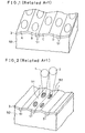
- FIG. I is a partially cut perspective view showing the related art proposed by the same assignee wherein the surface of the optical disk has oblique groove surfaces A, B, C, D,.., and a set of laser beam spots 1 and 2 as shown in FIG. 2 are irradiated on the oblique groove surfaces of each other neighboring relation with a ridge "r" inbetween to record information thereon and reproduce it therefrom.
- the two tracks e.g., oblique groove surfaces III and 112 may be used to record independent signals.
- header regions each with reference signals therein, which are permanently recorded by manufacturer, are provided on the disk.
- reference signals are address signal for searching a selected track, a sector signal for dividing the disk into several sectors, code signals for indicating that the opitcal disk is of constant angular velocity driving type or constant linear velocity driving type, or the like.
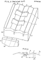
- the reference signal is generally recorded, as shown in FIG. 3, by forming pits 4 on the oblique surfaces of the V-shaped track.
- the optical recording disk having the V-section grooves is produced by cutting the helical or circular V-section grooves 51, 51 ... on a metal master disk, by means of a diamond cutter 55 having a V-shaped cutting edge 56. And then a stninper is produced by using the metal master having the helical or circular V-shape cross section grooves. And thereafter, by utilizing the stamper a substrate 50 is mass-produced by known plastic molding or the like manufacturing method.
- the pits 4 are formed to have round bottom face with respect to an imaginary cross-section of the pits in a direction of the longitudinal axis of the groove.
- the pits 4,4 are drawn to have rectangular shaped sections on a virtual sectional plane in the longitudinal direction of the groove as shown in F I G . 3 and subsequent drawings, FIGs. 5, 7 and 11, but actual shapes in virtual longitudinal sectional views the pits are shaped to have rounded corners which are like sinusoidal waves or deformed sinusoidal waves.
- Reproduction of reference signal by reading the pits is done by irradiating laser light beam spots on the signal tracks, namely the V-shaped groove 51, 51 having the pits 4, 4 ... thereon, and by detecting change of diffraction light obtained from the reflection from the disk surface.
- FIG. 4 is a front view of the V-shaped groove wherein the angle of V-shape of the grooves is 6, depth of the groove is "d", and lateral pitch of the groove is 2Pt.
- tan is given.
- the purpose of the present invention is to provide an improved optical disk and an improved method for reproducing reference signal from the optical disk.
- the improvements made in the present invention is to eliminate crosstalk between reference signals of neighboring V-shaped grooves, thereby to assure reliable reproduction of the reference signal which is very important to operation of the optical disk.
- Optical disk in sccordance with the present invention comprises:
- the method comprises the steps of
- FIG. 6(a), FIG. 6(B), FIG. 6(c), FIG. 7 and FIG. 8 show a first embodiment.
- FIG. 9, FIG. 10 and FIG. 11 show a second embodiment.
- FIG. 12, FIG. 13 and FIG. 14 show a third embodiment.
- FIG. 15 and FIG. 16 show a fourth embodiment.
- FIG. 17 shows a fifth embodiment.
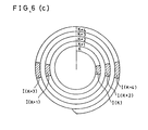
- FIG. 6(a) which shows disk format of the first embodiment
- a disk having a center hole 7 helical or circular V-shaped cross-section grooves are formed in a region between a periphery 5 and an innermost circle 6.
- the optical disk further has header regions 8 and 9 in the region between the periphery 5 and the innermost circle 6.
- the header regions 8 and 9 have permenently recorded reference signals, which are permanently recorded by changing depth of the V-shaped cross-section grooves. Manner of arrangement of the header regions 8 and 9 is shown in schematical enlargement in FIG. 6(b) and FIG. 6(c) which show cases of concentric type V-grooves and helical type V-grooves, respectively.
- numbers K, K+1, ...K+j show K-th, K+l-th, ... and K+j-th V-groove, respectively.
- I(K), I(K)+l, I(K)+2 ... I(K)+j show regions of reference signal for these V-grooves.
- two header regions are provided on the optical recording disk, and in one header region, the reference signal is recorded in the V-groove of odd number order, and in the other header reaion the reference signals are recorded in the V-groove of even number order.
- FIG. 7 shows in enlarged manner the parts wherein the reference signals are recorded.
- the photodetector 10 and 13 are configurated as has been disclosed in FIG. 6 of the European Patent Application 55439, and designated therein by marks M and N. Since reflected lights from the surface of the disk is diffracted by the pits on the tracks, intensities of reflected light received by the photodetector 10 and 13 change responding to existence or non-existence of the pits. Accordingly, by detecting the change of the intensity of the reflected light, the reference signal can be reproduced. In such detection, reference signals reproduced by the photodetector 10 and the second photodetector 13 are substantially the same. The same applies also in reproducing the reference signals recorded in the rightest V-groove III. Next, another case when a reference signal in the intermediate V-groove II is reproduced is described.
- a pair of the laser beam spots.I and II are irradiated on the track C and track D of the intermediate V-groove II, respectively.
- ridge line r bc is cut out by the pits of the V-groove I, and thereby width of the track C is decreased at the cut out parts.
- the width change APt of the track width Pt increases responding to increase ⁇ d of the pit depth "d". Accordingly, when the pit depth "d" increases to some extent, the laser beam spot 1 in the neighboring track C sufficiently detects the reference signal of the leftest V-groove.
- the laser beam spot 2 on the track D can detect the reference signal of neighboring V-groove III.
- the first photodetector 10 and the second photodetector 13 produce each other different reference signals based on the V-groove I and V-groove III. Therefore, a coincidence detector 17, which produces a coincidence signal between two signals based on the first photodetector 10 and the second photodetector 13 amplified by a first preamplifier 11 and a second preamplifier 14 and decoded by a first reference signal decoder 12 and a second reference signal decoder 15, fails to issue the coincidence output.
- the reproduced reference signal is a valid reference signal which is reproduced based on light beam scannings on a groove wherein the reference is recorded, or based on a scanning on a groove wherein the reference signal is not recorded.
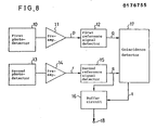
- FIG. 8 is a block diagram showing an example of a circuit for reproducing the reference signal, wherein output terminals of the first photodetector and the second photodetector are connected through a preamplifier 11 and a preamplifier 14 to input terminals of a first reference signal decoder 12 and a second reference signal decoder 15, respectively. And output terminals of the first reference signal decoder 12 and the second reference signal decoder 15 are connected to input terminals of a coincidence detector 17.
- the first photodetector 10 and the second photodetector 13 detect reflection light from the laser beam spots 1' and 2', and their output signals are amplified by the preamplifiers 11 and 14, to produce reproduced signal "p" and "r".
- the first reference signal decoder 12 and the second reference signal decoder 15 decode the reproduced reference signals "p" and “r” thereby to produce the reference signals "q” and “s", respectively.
- a buffer circuit 16 stores the output signal "s" from the second reference signal decoder 15, and when the coincidence detector 17 issues an output which indicates the reference signals "q” and “s” are identical each other thereby issuing a coincidence signal "a”, then issues the temporarily stored signal "s" to its output terminal 18.
- two reference signals obtained by the pair of laser light beams scanning on neighboring two tracks are examined with respect to their coincidence, and when the coincidence is confirmed the reference signal is outputted as a valid reference signal.
- the address signal comprises a code signal of address value to show each V-groove, address mark signal to show starting points of address regions, error correction code for detecting and correcting errors generated at producing of the code signal, clock synchronization signal, or the like.
- the address signal is preferably recorded for every certain data length of a recorded signal.
- distance between the reference signal I(K) and I(K+l) is one and half ,turn, while a distance between I(K+1) and I(K+2) is only half turn. Therefore, the length of the data recording region is not uniformed with respect to each groove.
- a modified disk format as shown in FIG. 9 is proposed.
- the header region 19 disposed in a region including one radius has a recording of reference signal including address signal.
- the optical recording disk shown in FIG. 9 is.for use in a constant angular velocity driving (hereinafter is referred to as CAV driving).
- CAV driving constant angular velocity driving
- the header region is disposed on a radius as shown in FIG. 9.
- FIG. 10 is an enlarged perspective view showing a small part of the disk surface whereon the header region disposed on the radius is shown.
- bit number of the address signal is L
- the header region 19 has a physical length for enabling cutting for information of 2L bits.
- the header region 19 is divided into several sets each consisting of two parts 20 vs. 21, two parts of 22 vs. 23, etc., and the regions of the address signal are disposed like in a checker pattern as shown in FIG. 10, that is, the header regions are disposed with respect to a radius line in alternate V-grooves in radial direction, so that pits of each other neighboring V-grooves do not conflict each other.
- FIG. 11 is a plan view showing a small part of the header region formed in the above-mentioned manner.
- FIG. 12 A third example is described hereafter with reference to FIG. 12, FIG. 13 and FIG. 14.
- This third embodiment relates to an optical recording disk of constant linear velocity type (hereinafter is abbreviated as CLV-type).
- CLV-type constant linear velocity type
- the hatched regions show header regions and 28, 29, 30 and 31 show V-grooves proved that unitary length of data length of the recording signal is l byte, phisical length of V-groove necessary for recording it is always the same irrespective of the position of the grooves being near periphery or near center.
- this unit length to be RL and that the length RL includes address of the signal.
- FIG. 13 shows a small part of the optical recording disk wherein three neighboring header regions in neighboring three V-grooves V 0 , V 1 and V 2 .
- radial distance (pitch) of neighboring V-grooves is 2P
- distance difference 6 along herical or circular V-groove between the observed V-grooved V 1 and adjacent outer V-groove V 2 or adjacent inner V-groove V 0 is about 2 ⁇ -2P.
- the distance difference 6 is ⁇ ⁇ 10 ⁇ m.
- the neighboring header regions become partly contacting each other in radial direction as shown in FIG. 13, and therefore due to the aofrementioned reason in the preceding example a reading of address signal becomes difficult.
- the lengths of the header regions are selected to be twice the physical length necessary for cutting the address signal thereon plus 6, that is 2AR+6, and that the header region is divided into two parts, i.e., central part 32 having no address signal and either one end regions having address signals.
- the forming of the address signals is made by selecting former half part, latter half part, former half part, ... in the address cutting regions of the header regions 25 so that the address signal parts 33, 34, 35 ... are not formed radially continuous.
- the address signals recorded by the above-mentioned CAV type or CLV type optical recording disk can be reproduced in similar way as that described with reference to the circuit of reference signal reproducing of FIG. 8.
- the address value of the optical recording disk are recorded by regularly changing at every precletermined data length. Therefore, even though all the addresses are not recorded, address values can be repro ducved by interpolating from the address values of previous or susequent positions. As an example of such way, a description is made on a case wherein address values are alloted in sequential order on a row of V-grooves on the optical recording disk, and the address signal is recorded in every other V-grooves. In this case, in the configuration of the optical recording disk shown in FIG.
- This type of recording is a recording type wherein among two header regions 8 and 9 of - FIG. 6(a), only one is used for recording, and in this type of recording there is no possibility that two address signals in the each other neighboring V-grooves conflict each other. And hence, this type recording produces no cross talk.
- FIG. 15 is a circuit block diagram showing one example of a circuit for reproducing the address signal of this fourth example.
- the circuit of this example comprises address region detectors 36 and 39, address decoder 37 and 40 and an interpolator 38 which issues output signal to an output terminal 41 Similar to the circuit of FIG. 8, the first photodetect; 10 and the second photodetector 13 detects reflected lights of the laser beam spots 1 and 2, respectively. The first and the second photodetector 10 and 13 issue electric signals to the preamplifiers 11 and 14, thereby issuing output signals PI and P2.
- the address region detector 36 and 39 detect address mark signals from the output signals P1 and P2, respectively, thereby issuing address gate signals ul and u2, which are given to the address decorder 37 and 40, respectively.
- These address decoders 37 and 40 issues output address values adl and ad2 to the interpolator 38.
- the interpolator 38 examines whether the first address value ad1 and the second address value ad2 coincide each other. Then, when the coincidence is obtained, the interpolator 38 issues the address value to the output terminal 41 as an address value v of the V-groove II being scanned by the pnir of the lasor beams 1 and 2. On the contrary, when the coincidence is not obtained, the address value v of the V-groove is produced by the predetermined. interpolation process using two address values adl and ad2, and such interpolated output v is issued to the output terminal 41.
- the reproduced signals P1 and P2 are further used to reproduce data signal other than the address signal reproducing, and therefore is given to a known signal reproducing circuit (not shown in FIG. 15).
- the interpolation process is dependent on the recording method of address values on the optical recording disk. Now in this example, let us provide that the address signal is recorded in track of every other V-grooves.
- FIG. 16 one example of the interpolation circuit is shown in FIG. 16.
- the circuit of FIG. 16 has two address decoders 37 and 40 which give output signals to an interpolator 38.
- the components and parts corresponding to those of FIG. 15 are designated by the same numerals.
- the interpolator 38 has an adder 42 and a divider 43 connected in sequence.
- the address decoders 37 and 40 reproduce output signals ad1 and ad2 respectively.
- the adder 42 makes addition of the address values ad1 and ad2.
- the divider 43 divides the added value by 2, and output the divided value to the output terminal 41 as the - address value v.
- the address value ad1 becomes address n
- the address value ad2 becomes n+2. Therefore by obtaining arithmetic mean of these two address values, the address value v of the V groove II is obtainable to be n+1.
- FIG. 17 shows another example of the optical disk format wherein the corresponding parts are designated by the same numerals with the preceding examples, for instance FIG. 9.
- the optical recording disk of FIG. 17 is divided to k sectors.
- k is 8.
- the address is alloted for respective sectors.
- address values of plural V-grooves which are adjoining within one sector separated by the sector separators vary by addresses of K.
- the interpolator 38 can be constituted in a ROM, and a predetermined address values are preliminarily written in the ROM.
- the address signal is to be reproduced, it is done by reading out the written data by means of the address values ad1 and ad2 as the addresses of the ROM, and the read out address value v is used as the address of the V-groove which is looked for.
- the apparatus and method in accordance with the present invention can record and readout reference signals without any trouble of making interferences between neighboring V-grooves, and very accurate reading is achievable by using coincidence of the reference- signals read by two laser beam spots.
- address signals of the V-grooves having no recording of the address signal can be obtained by means of interpolation. Accordingly, practical utility of using the above mentioned method of recording on an optical recording disk well as method of reproducing the reference signal the optical I recording is very great.
Abstract
Description
- The present invention relates generally to optical disks and method for reproducing reference signal therefrom, and more particularly to optical recording disks having circular or helical (i.e., spiral) grooves of V-section whereon recording signals are recorded, for example as change of optical reflectivity or forming pits or change of optomagnetic characteristic and reference signals are recorded by forming pits on the surface of the V-section grooves and method for reproducing the reference signal therefrom.
- In recent years, various optical disk memory means for recording and reproducing information by using laser light on a disk have been proposed. Among them, as method for improving recording density and transfer rate in recording and reproducing, we have proposed method for recording and reproducing signal by utilizing oblique surface of helical or circular grooves having V-shaped section with respect to an imaginary sectional plane in radial direction (Japanese Patent Unexamined Published
- Application 59-36338).
- FIG. I is a partially cut perspective view showing the related art proposed by the same assignee wherein the surface of the optical disk has oblique groove surfaces A, B, C, D,.., and a set of
laser beam spots thin film 3 is, for instance TeOx (x =l.l), and by changing reflectivity of the small areas on the track by producing reaction by the laser beam spots, recording of signal can be made. - When the signal recorded in the above-mentioned way is reproduced by scanning by laser beam spots on each other neighboring tracks on neighboring oblique surfaces of the recording groove in the similar way as in the recording, signals recorded on the two tracks are simultaneously reproduced, and such signals are usable, for instance, to obtain a transfer rate as high as twice of the single track optical disk system. As has been described in the Published European Patent Application 55439, by optimumly selecting the shape of the V-section groove, crosstalk from neighboring oblique surface through receiving mainly positive or negative first diffraction lights among reflection lights from the disk is sufficiently suppressed, and each signal of respective tracks can be individually reproduced. In such reproducing, a photodetector to be used is known by being disclosed in FIG. 6 of the Published European Patent Application No. 55439.
- In general, in an optical recording disk, beside the information recording track for use for user to record desired data, header regions each with reference signals therein, which are permanently recorded by manufacturer, are provided on the disk. For instance, such reference signals are address signal for searching a selected track, a sector signal for dividing the disk into several sectors, code signals for indicating that the opitcal disk is of constant angular velocity driving type or constant linear velocity driving type, or the like.
- The reference signal is generally recorded, as shown in FIG. 3, by forming
pits 4 on the oblique surfaces of the V-shaped track. Generally, the optical recording disk having the V-section grooves is produced by cutting the helical or circular V-section grooves shaped cutting edge 56. And then a stninper is produced by using the metal master having the helical or circular V-shape cross section grooves. And thereafter, by utilizing the stamper asubstrate 50 is mass-produced by known plastic molding or the like manufacturing method. Thepits pits 4 are formed to have round bottom face with respect to an imaginary cross-section of the pits in a direction of the longitudinal axis of the groove. However, for the sake of easy drawing and clear understanding of the shape of the pits, thepits - Reproduction of reference signal by reading the pits is done by irradiating laser light beam spots on the signal tracks, namely the V-
shaped groove pits - In the above-mentioned conventional method of forming the pits for recording the reference signal, since the diamond cutter has a very large width in comparison with width of each V-shaped cross-section groove, forming of the pits on one V-shaped cross-section groove inevitably produce partial cutting of upper edge parts of neighboring V-shaped cross-section grooves B and E, thereby undesirably producing a cause of crosstalk in reproducing of neighboring tracks.
- This is elucidated more in detail with reference to FIG. 4, which is a front view of the V-shaped groove wherein the angle of V-shape of the grooves is 6, depth of the groove is "d", and lateral pitch of the groove is 2Pt. Let us take one example wherein


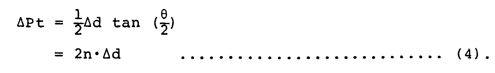
- In the case shown in FIG. 4, when a pit is formed in the groove V1 the ridge r is shifted rightward by ΔPt, thereby broadening the width Pt of the track to Pt+ΔPt. When another pit is formed on a groove V2, which is on the rightside of the former groove V 1, the ridge r is shifted leftward by ΔPt, thereby narrowing the width Pt of the track to Pt-ΔPt. That is, the width of the track changes from P+ΔPt to P-ΔPt, and the changes in total range 2ΔPt.
- This equation gives a result that when n=1.5, lateral increase of the pitch is three times of the depth of pits, and therefore a track pitch Pt changes by 2 Pt=6Ad. For instance, when Δd=0.02 µm , 2 ΔPt=0.12 µm results. Since the track pitch Pt is about 1 pm, such change of the position of ridge between the tracks results in substantial crosstalk. Especially in the case of FIG. 5, wherein pits in neighboring tracks are interfering each other, there is a grave possibility of erroneous reading of the reference signal induced by the interfering dispositions of the pits in neighboring tracks.
- The purpose of the present invention is to provide an improved optical disk and an improved method for reproducing reference signal from the optical disk. The improvements made in the present invention is to eliminate crosstalk between reference signals of neighboring V-shaped grooves, thereby to assure reliable reproduction of the reference signal which is very important to operation of the optical disk.
- Optical disk in sccordance with the present invention comprises:
- a disk having grooves of helical or circular pattern and of V-shaped cross-section thereon,
- header regions on at least one of the helical and circular grooves having reference signals recorded in form of pits that are parts with changed depth across width of the helical or circular grooves,
- the parts with changed depth are disposed in a manner that parts which has the reference signals of each-other-neighboring grooves are apart from each other in longitudinal direction of said groove.
- In method in accordance with the present invention for reproducing reference signal from a recording disk which has grooves of helical or circular pattern and of V-shaped cross section thereon, each of the groove having two recording tracks on oblique surface therein, the method comprises the steps of
- irradiating two light beams on pits of reference signals in a header region on two neighboring tracks of oblique surface on helical or circular grooves of V-shaped section wherein the pits are disposed in a manner that the parts of each-other-neighboring grooves are apart from each other in longitudinal direction of the groove,
- detecting reflection light from the tracks and producing two electric signals corresponding to data on respective two tracks and
- detecting coincidence between the two electric signals thereby to produce a valid reference signals only when the two electric signals coincide each other.
-
- FIG. I is the perspective view of the small part of the optical recording disk with V-shaped cross-section grooves of the related art.
- FIG. 2 is the perspective view of the small part irradiated with a pair of laser beams in the related art.
- FIG. 3 is the perspectrive view of the small part having reference signal pits for permanently recording reference signal as ohange of depth of V-shaped cross-section grooves in the related art.
- FIG. 4 is the schematic view showing relation of width variation corresponding to depth variation of the V- shaped cross-section groove of FIG. 3.
- FIG. 5 is the perspective view of a small part of a recording disk of a related art wherein pits of neighboring grooves are overlapping.
- FIG. 6(a), FIG. 6(b) and FIG. 6(c) are schematic plan views of disk format of various embodiment embodying the present invention.
- FIG. 7 is a perspective view of a small part of an optical recording disk embodying the present invention showing relation between reference signal pits and data signal spots.
- FIG. 8 is a circuit block diagram of one example of a reference signal reproducing circuit in one embodiment of the present invention.
- FIG. 9 is schematic plan views showing disk formats of a second embodiment in accordance with the present invention.
- FIG. 10 is a perspective view of a small part of an optical recording disk of the second embodiment showing header regions.
- FIG. 11 is a schematic plan view of a small part of an optical recording disk showing arrangement of the reference signal pits, wherein vertical size of the drawing is represented very much compressed.
- FIG. 12 is a schematic plan view showing arrangement of reference signal pits in a third embodiment.
- FIG. 13 is a perspective view of a small part of an optical recording disk of related art showing staggered arrangement of header region on a CLV disk.
- FIG. 14 is a perspective view of a small part of an optical recolrding disk of the third embodiment showing an improved arrangement of the header region embodying the present invention.
- FIG. 15 is a circuit block diagram showing one example of an address reproducing circuit of a fourth embodiment.
- FIG. 16 is a circuit block diagram showing address interpolation circuit of the fourth embodiment in accordance with the present invention.
- FIG. 17 is a schematic plan view showing a disk format of a fifth embodiment of an optical recording disk embodying the present invention.
- Hereafter, the invention is described in detail taking several embodiments with reference to the accompanying drawings FIG. 6(a), FIG. 6(B), FIG. 6(c), FIG. 7 and FIG. 8 show a first embodiment. FIG. 9, FIG. 10 and FIG. 11 show a second embodiment. FIG. 12, FIG. 13 and FIG. 14 show a third embodiment. FIG. 15 and FIG. 16 show a fourth embodiment. FIG. 17 shows a fifth embodiment.
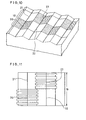
- In FIG. 6(a) which shows disk format of the first embodiment, on a disk having a
center hole 7, helical or circular V-shaped cross-section grooves are formed in a region between aperiphery 5 and aninnermost circle 6. The optical disk further hasheader regions periphery 5 and theinnermost circle 6. As is already known, theheader regions header regions - And hatched regions I(K), I(K)+l, I(K)+2 ... I(K)+j show regions of reference signal for these V-grooves. In this embodiment, two header regions are provided on the optical recording disk, and in one header region, the reference signal is recorded in the V-groove of odd number order, and in the other header reaion the reference signals are recorded in the V-groove of even number order. By arranging the reference signals in the above-mentioned manner, undesirable crosstalking of the reference signals between neighboring V-grooves can be avoided.
- Method for reproducing the reference signals recorded in the above-mentioned way is described hereafter.
- FIG. 7 shows in enlarged manner the parts wherein the reference signals are recorded.
- In FIG. 7, in a leftest V-groove I consisting of tracks A and B and a rightest V-groove III have reference signals recorded by forming pits which are made by changing depth of the V-groove I and III. On the contrary, in the intermediate V-groove II, no reference signal is recorded. A case when the reference signal in the leftest V-groove I is reproduced is first elucidated. Now provided that a
laser beam spot 1 is formed on the track A and anotherlaser beam spot 2 is formed on a neighboring track B, reflected lights from the laser beam spots I and 2 are detected by afirst photodetector 10 and asecond photodetector 13, respectively as shown in FIG. 8. Thephotodetector photodetector photodetector 10 and thesecond photodetector 13 are substantially the same. The same applies also in reproducing the reference signals recorded in the rightest V-groove III. Next, another case when a reference signal in the intermediate V-groove II is reproduced is described. As shown in FIG. 7, a pair of the laser beam spots.I and II are irradiated on the track C and track D of the intermediate V-groove II, respectively. In this case, as shown in FIG. 7, ridge line rbc is cut out by the pits of the V-groove I, and thereby width of the track C is decreased at the cut out parts. As has been described with reference to the aforementioned equation (4), the width change APt of the track width Pt increases responding to increase Δd of the pit depth "d". Accordingly, when the pit depth "d" increases to some extent, thelaser beam spot 1 in the neighboring track C sufficiently detects the reference signal of the leftest V-groove. In the same manner, thelaser beam spot 2 on the track D can detect the reference signal of neighboring V-groove III. In such undesirable detections of the reference signals of neighboring tracks, thefirst photodetector 10 and thesecond photodetector 13 produce each other different reference signals based on the V-groove I and V-groove III. Therefore, acoincidence detector 17, which produces a coincidence signal between two signals based on thefirst photodetector 10 and thesecond photodetector 13 amplified by afirst preamplifier 11 and asecond preamplifier 14 and decoded by a first reference signal decoder 12 and a secondreference signal decoder 15, fails to issue the coincidence output. In the above-mentioned manner, by producing the coincidence detection signal between the signals based on thefirst photodetector 10 and thesecond photodetector 13, judgment is made whether the reproduced reference signal is a valid reference signal which is reproduced based on light beam scannings on a groove wherein the reference is recorded, or based on a scanning on a groove wherein the reference signal is not recorded. - FIG. 8 is a block diagram showing an example of a circuit for reproducing the reference signal, wherein output terminals of the first photodetector and the second photodetector are connected through a
preamplifier 11 and apreamplifier 14 to input terminals of a first reference signal decoder 12 and a secondreference signal decoder 15, respectively. And output terminals of the first reference signal decoder 12 and the secondreference signal decoder 15 are connected to input terminals of acoincidence detector 17. As has been described with reference to FIG. 7, thefirst photodetector 10 and thesecond photodetector 13 detect reflection light from the laser beam spots 1' and 2', and their output signals are amplified by thepreamplifiers reference signal decoder 15 decode the reproduced reference signals "p" and "r" thereby to produce the reference signals "q" and "s", respectively. Abuffer circuit 16 stores the output signal "s" from the secondreference signal decoder 15, and when thecoincidence detector 17 issues an output which indicates the reference signals "q" and "s" are identical each other thereby issuing a coincidence signal "a", then issues the temporarily stored signal "s" to itsoutput terminal 18. As a result of the above-mentioned circuit configuration and signal processing, two reference signals obtained by the pair of laser light beams scanning on neighboring two tracks are examined with respect to their coincidence, and when the coincidence is confirmed the reference signal is outputted as a valid reference signal. - In general, in the reference signal, many information are contained, and among them the signal which has largest information amount is address signal. The address signal comprises a code signal of address value to show each V-groove, address mark signal to show starting points of address regions, error correction code for detecting and correcting errors generated at producing of the code signal, clock synchronization signal, or the like.
- The address signal is preferably recorded for every certain data length of a recorded signal. However, for instance, in the case of FIG. 6(c), distance between the reference signal I(K) and I(K+l) is one and half ,turn, while a distance between I(K+1) and I(K+2) is only half turn. Therefore, the length of the data recording region is not uniformed with respect to each groove. In order to improve the above-mentioned problem, a modified disk format as shown in FIG. 9 is proposed. In the optical recording disk shown in FIG. 9, the
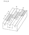
header region 19 disposed in a region including one radius has a recording of reference signal including address signal. The optical recording disk shown in FIG. 9 is.for use in a constant angular velocity driving (hereinafter is referred to as CAV driving). In case the signal recording and reproducing are made by the CAV driving, the header region is disposed on a radius as shown in FIG. 9. - FIG. 10 is an enlarged perspective view showing a small part of the disk surface whereon the header region disposed on the radius is shown. When bit number of the address signal is L, the
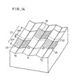
header region 19 has a physical length for enabling cutting for information of 2L bits. In the example of FIG. 10, theheader region 19 is divided into several sets each consisting of twoparts 20 vs. 21, two parts of 22 vs. 23, etc., and the regions of the address signal are disposed like in a checker pattern as shown in FIG. 10, that is, the header regions are disposed with respect to a radius line in alternate V-grooves in radial direction, so that pits of each other neighboring V-grooves do not conflict each other. FIG. 11 is a plan view showing a small part of the header region formed in the above-mentioned manner. - A third example is described hereafter with reference to FIG. 12, FIG. 13 and FIG. 14. This third embodiment relates to an optical recording disk of constant linear velocity type (hereinafter is abbreviated as CLV-type). In FIG. 12, the hatched regions show header regions and 28, 29, 30 and 31 show V-grooves proved that unitary length of data length of the recording signal is ℓ byte, phisical length of V-groove necessary for recording it is always the same irrespective of the position of the grooves being near periphery or near center. Now let us define this unit length to be RL and that the length RL includes address of the signal. In this type of the optical recording disk, though the header regions are not disposed simply on one radius of the recording disk, still there are possibilities that the neighboring header regions are disposed each other contacting in fully or partly in radial direction. FIG. 13 shows a small part of the optical recording disk wherein three neighboring header regions in neighboring three V-grooves V0, V1 and V2. Now provided that radial distance (pitch) of neighboring V-grooves is 2P,
distance difference 6 along herical or circular V-groove between the observed V-grooved V 1 and adjacent outer V-groove V2 or adjacent inner V-groove V0 is about 2π-2P. When 2P is 1.6 µm, thedistance difference 6 is δ ≒ 10 µm. When length of recording part of the address signal AR is longer than thediscance 6, the neighboring header regions become partly contacting each other in radial direction as shown in FIG. 13, and therefore due to the aofrementioned reason in the preceding example a reading of address signal becomes difficult. In order to dissolve the above-mentioned problem, as shown in FIG. 14 the lengths of the header regions are selected to be twice the physical length necessary for cutting the address signal thereonplus 6, that is 2AR+6, and that the header region is divided into two parts, i.e.,central part 32 having no address signal and either one end regions having address signals. By so arranging the header regions, the forming of the address signals is made by selecting former half part, latter half part, former half part, ... in the address cutting regions of theheader regions 25 so that theaddress signal parts - The address signals recorded by the above-mentioned CAV type or CLV type optical recording disk can be reproduced in similar way as that described with reference to the circuit of reference signal reproducing of FIG. 8.
- In general, the address value of the optical recording disk are recorded by regularly changing at every precletermined data length. Therefore, even though all the addresses are not recorded, address values can be repro ducved by interpolating from the address values of previous or susequent positions. As an example of such way, a description is made on a case wherein address values are alloted in sequential order on a row of V-grooves on the optical recording disk, and the address signal is recorded in every other V-grooves. In this case, in the configuration of the optical recording disk shown in FIG. 7, when the address value of the V-groove I is address n (n is an integer), and address value of the V-
groove 3 is n+2, in the same manner the address values are designed to increase by 2 for every two-groove displacement of the V-groove. This type of recording is a recording type wherein among twoheader regions - Next, method of reproducing the address signals recorded in the above-mentioned way is elucidated. When the address signals recorded on the V-grooves I and III as shown in FIG. 7, address signals reproduced by using a pair of the laser beam spots coincide with each other. And therefore it is determined that the reproduced address signals is right one which is recorded on tracks which are in the same V-groove. On the contrary, when reproducing of signal is carried out on the V-groove II wherein no address signals are recorded, a pair of the laser beam spots reproduce the address signals of the neighboring V-grooves I and III by detecting cross talk noises due to the tresspassing edges of the pits beyond the ridges between the different V-grooves. Address values of the V-groove II is obtainable by an interpolation using the address values of the V-groove I and the V-groove III.
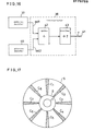
- FIG. 15 is a circuit block diagram showing one example of a circuit for reproducing the address signal of this fourth example. In the circuit block diagram of FIG. 15, corresponding components and parts with the previous example of FIG. 8 are shown by the same numerals. The circuit of this example comprises
address region detectors address decoder interpolator 38 which issues output signal to an output terminal 41 Similar to the circuit of FIG. 8, the first photodetect; 10 and thesecond photodetector 13 detects reflected lights of thelaser beam spots second photodetector preamplifiers address region detector address decorder address decoders interpolator 38. Theinterpolator 38 examines whether the first address value ad1 and the second address value ad2 coincide each other. Then, when the coincidence is obtained, theinterpolator 38 issues the address value to the output terminal 41 as an address value v of the V-groove II being scanned by the pnir of the lasor beams 1 and 2. On the contrary, when the coincidence is not obtained, the address value v of the V-groove is produced by the predetermined. interpolation process using two address values adl and ad2, and such interpolated output v is issued to the output terminal 41. - Incidentaly, in the circuit of FIG. 15 the reproduced signals P1 and P2 are further used to reproduce data signal other than the address signal reproducing, and therefore is given to a known signal reproducing circuit (not shown in FIG. 15).
- Next, the process of interpolation of the address value is described. The interpolation process is dependent on the recording method of address values on the optical recording disk. Now in this example, let us provide that the address signal is recorded in track of every other V-grooves.
- one example of the interpolation circuit is shown in FIG. 16. The circuit of FIG. 16 has two
address decoders interpolator 38. The components and parts corresponding to those of FIG. 15 are designated by the same numerals. Theinterpolator 38 has anadder 42 and adivider 43 connected in sequence. As has been described on FIG. 15, theaddress decoders adder 42 makes addition of the address values ad1 and ad2. Thedivider 43 divides the added value by 2, and output the divided value to the output terminal 41 as the - address value v. In general, such computation is made by binary code, and therefore the dividing by thedivider 43 is made by only shifting the added result by one bit toward LSB. When the address signal of the V-groove I of FIG. 7 is reproduced by this interpolation ciricuit of FIG. 16, both address alues ad1 and ad2 become n. Accordingly the address value v after the interpolation processing is also of n. When the address value in the V-groove III is reproduced, the address value v becomes n+2 in the similar way. - Next, when the address value on the V-groove II is reproduced, the address value ad1 becomes address n, and the address value ad2 becomes n+2. Therefore by obtaining arithmetic mean of these two address values, the address value v of the V groove II is obtainable to be n+1.
- Recording method of the address value varies depending on formats of the optical recording disk. FIG. 17 shows another example of the optical disk format wherein the corresponding parts are designated by the same numerals with the preceding examples, for instance FIG. 9. The optical recording disk of FIG. 17 is divided to k sectors. In the example k is 8. For the sake of recording and reproducing of the data signal and serching it., it is convenient to control the data signal in sector by sector basis. Accordingly, the address is alloted for respective sectors. In this case, address values of plural V-grooves which are adjoining within one sector separated by the sector separators vary by addresses of K. In this case, by recording the address signals in a manner to advance by address of 2k, for instance, address nt2k after address n and the like. Then, by the interpolator circuit shown in FIG. 16, the address values of respective V-grooves are obtainable in the same way.
- When the series of the address values are not in the above-mentioned arithmetical series, the above mentioned interpolator circuit can not be used. In general, the
interpolator 38 can be constituted in a ROM, and a predetermined address values are preliminarily written in the ROM. When the address signal is to be reproduced, it is done by reading out the written data by means of the address values ad1 and ad2 as the addresses of the ROM, and the read out address value v is used as the address of the V-groove which is looked for. - As has been described in detail on preferred embodiments, the apparatus and method in accordance with the present invention can record and readout reference signals without any trouble of making interferences between neighboring V-grooves, and very accurate reading is achievable by using coincidence of the reference- signals read by two laser beam spots. Besides, in the case of recording the address signals in every other V-grooves, by utilizing crosstalk of the address signals in neighboring V-grooves, address signals of the V-grooves having no recording of the address signal can be obtained by means of interpolation. Accordingly, practical utility of using the above mentioned method of recording on an optical recording disk well as method of reproducing the reference signal the optical I recording is very great.
characterized in that
Claims (9)
charactrereized in that
Applications Claiming Priority (4)
| Application Number | Priority Date | Filing Date | Title |
|---|---|---|---|
| JP59181752A JPS6161237A (en) | 1984-08-31 | 1984-08-31 | Optical disk and address reproduction method of optical disk |
| JP181752/84 | 1984-08-31 | ||
| JP59259478A JPS61137242A (en) | 1984-12-07 | 1984-12-07 | Optical disk and address recording and reproducing method |
| JP259478/84 | 1984-12-07 |
Publications (3)
| Publication Number | Publication Date |
|---|---|
| EP0176755A2 true EP0176755A2 (en) | 1986-04-09 |
| EP0176755A3 EP0176755A3 (en) | 1987-03-25 |
| EP0176755B1 EP0176755B1 (en) | 1989-12-06 |
Family
ID=26500802
Family Applications (1)
| Application Number | Title | Priority Date | Filing Date |
|---|---|---|---|
| EP85110716A Expired EP0176755B1 (en) | 1984-08-31 | 1985-08-26 | Optical disk and method for reproducing reference signal therefrom |
Country Status (3)
| Country | Link |
|---|---|
| US (1) | US4712204A (en) |
| EP (1) | EP0176755B1 (en) |
| DE (1) | DE3574644D1 (en) |
Cited By (7)
| Publication number | Priority date | Publication date | Assignee | Title |
|---|---|---|---|---|
| EP0193614A1 (en) * | 1984-09-04 | 1986-09-10 | Matsushita Electric Industrial Co., Ltd. | Disk-shaped record carrier |
| US4873679A (en) * | 1986-12-25 | 1989-10-10 | Matsushita Electric Industrial Co., Ltd. | Optical information recording disk and optical information recording disk apparatus |
| EP0499278A2 (en) * | 1991-02-14 | 1992-08-19 | Sony Corporation | Method for recording sector control information on magneto-optical disk |
| EP0570235A3 (en) * | 1992-05-15 | 1994-01-05 | Sharp Kabushiki Kaisha | Optical disk |
| EP0656625A1 (en) * | 1993-12-01 | 1995-06-07 | Sharp Kabushiki Kaisha | Optical disk and method for reproducing information recorded on the same |
| EP0588305A3 (en) * | 1992-09-14 | 1996-01-03 | Matsushita Electric Ind Co Ltd | Optical information recording medium and optical information recording/reproducing apparatus |
| EP0757343A1 (en) * | 1995-02-17 | 1997-02-05 | Matsushita Electric Industrial Co., Ltd. | Optical disk and optical disk recording and reproducing device |
Families Citing this family (13)
| Publication number | Priority date | Publication date | Assignee | Title |
|---|---|---|---|---|
| JPH0782703B2 (en) * | 1986-08-01 | 1995-09-06 | パイオニア株式会社 | Crosstalk noise measurement method |
| US4949325A (en) * | 1987-03-18 | 1990-08-14 | Hitachi, Ltd. | Method and associated apparatus and medium for optical recording and reproducing information |
| JPH01130324A (en) * | 1987-11-16 | 1989-05-23 | Olympus Optical Co Ltd | Optical recording and reproducing device |
| JP2589370B2 (en) * | 1989-04-13 | 1997-03-12 | シャープ株式会社 | Optical disk drive |
| JPH02292744A (en) * | 1989-05-02 | 1990-12-04 | Teac Corp | Optical disk and optical disk device |
| JP2572842B2 (en) * | 1989-05-10 | 1997-01-16 | パイオニア株式会社 | Apparatus for detecting crosstalk in optical read signal |
| US5134601A (en) * | 1989-08-08 | 1992-07-28 | International Business Machines Corporation | Optical disk sector servo patterns |
| US5214629A (en) * | 1990-02-27 | 1993-05-25 | Hitachi Maxell, Ltd. | Optical disc having a high-speed access capability and reading apparatus therefor |
| US5422762A (en) * | 1992-09-30 | 1995-06-06 | Hewlett-Packard Company | Method and apparatus for optimizing disk performance by locating a file directory on a middle track and distributing the file allocation tables close to clusters referenced in the tables |
| EP0628952B1 (en) * | 1993-06-08 | 2002-02-20 | Matsushita Electric Industrial Co., Ltd. | Optical disk, and information recording/reproduction apparatus |
| US5615205A (en) * | 1995-06-28 | 1997-03-25 | International Business Machines Corporation | Bi-level optical media having embossed header format |
| US7088668B1 (en) * | 1999-10-19 | 2006-08-08 | Matsushita Electric Industrial Co., Ltd. | Optical recording medium with address information composed of pits |
| KR100667764B1 (en) * | 2004-10-08 | 2007-01-12 | 삼성전자주식회사 | Optical recording medium, recording/reproducing method and recording/reproducing apparatus |
Citations (5)
| Publication number | Priority date | Publication date | Assignee | Title |
|---|---|---|---|---|
| US3992593A (en) * | 1974-08-22 | 1976-11-16 | Heine William K | Disc phonograph record playback by laser generated diffraction pattern |
| US4006292A (en) * | 1974-09-03 | 1977-02-01 | Sharp Corporation | Information recording and reproducing system with plural information tracks within a single groove |
| US4310916A (en) * | 1979-09-27 | 1982-01-12 | U.S. Philips Corporation | Optical record carrier and apparatus for reading it |
| EP0102231A1 (en) * | 1982-08-24 | 1984-03-07 | Matsushita Electric Industrial Co., Ltd. | Optical disk and method of recording and reproduction for the disk |
| US4455632A (en) * | 1980-04-25 | 1984-06-19 | U.S. Philips Corporation | Apparatus for optically reading a record carrier with two types of information areas |
Family Cites Families (4)
| Publication number | Priority date | Publication date | Assignee | Title |
|---|---|---|---|---|
| FR2325262A1 (en) * | 1974-01-11 | 1977-04-15 | Thomson Brandt | PROCESS FOR ENTERING TELEVISION SIGNALS ON AN INFORMATION AND RECORDING MEDIA OBTAINED BY LEDIT PROCEDE |
| GB1577133A (en) * | 1976-03-19 | 1980-10-22 | Rca Corp | Video information record and playback apparatus |
| JPS57105828A (en) * | 1980-12-19 | 1982-07-01 | Matsushita Electric Ind Co Ltd | Optical disk recording and reproducing system |
| JPS58175109A (en) * | 1982-04-07 | 1983-10-14 | Pioneer Video Kk | Recording system of discoidal recording medium |
-
1985
- 1985-08-23 US US06/768,843 patent/US4712204A/en not_active Expired - Lifetime
- 1985-08-26 EP EP85110716A patent/EP0176755B1/en not_active Expired
- 1985-08-26 DE DE8585110716T patent/DE3574644D1/en not_active Expired - Lifetime
Patent Citations (5)
| Publication number | Priority date | Publication date | Assignee | Title |
|---|---|---|---|---|
| US3992593A (en) * | 1974-08-22 | 1976-11-16 | Heine William K | Disc phonograph record playback by laser generated diffraction pattern |
| US4006292A (en) * | 1974-09-03 | 1977-02-01 | Sharp Corporation | Information recording and reproducing system with plural information tracks within a single groove |
| US4310916A (en) * | 1979-09-27 | 1982-01-12 | U.S. Philips Corporation | Optical record carrier and apparatus for reading it |
| US4455632A (en) * | 1980-04-25 | 1984-06-19 | U.S. Philips Corporation | Apparatus for optically reading a record carrier with two types of information areas |
| EP0102231A1 (en) * | 1982-08-24 | 1984-03-07 | Matsushita Electric Industrial Co., Ltd. | Optical disk and method of recording and reproduction for the disk |
Cited By (13)
| Publication number | Priority date | Publication date | Assignee | Title |
|---|---|---|---|---|
| EP0193614A1 (en) * | 1984-09-04 | 1986-09-10 | Matsushita Electric Industrial Co., Ltd. | Disk-shaped record carrier |
| EP0193614B1 (en) * | 1984-09-04 | 1991-01-30 | Matsushita Electric Industrial Co., Ltd. | Disk-shaped record carrier |
| US4873679A (en) * | 1986-12-25 | 1989-10-10 | Matsushita Electric Industrial Co., Ltd. | Optical information recording disk and optical information recording disk apparatus |
| EP0499278A2 (en) * | 1991-02-14 | 1992-08-19 | Sony Corporation | Method for recording sector control information on magneto-optical disk |
| EP0499278A3 (en) * | 1991-02-14 | 1993-08-11 | Sony Corporation | Method for recording sector control information on magneto-optical disk |
| EP0851416A3 (en) * | 1992-05-15 | 1999-03-24 | Sharp Kabushiki Kaisha | Optical disk and method of manufacturing an optical disk |
| EP0570235A3 (en) * | 1992-05-15 | 1994-01-05 | Sharp Kabushiki Kaisha | Optical disk |
| EP0588305A3 (en) * | 1992-09-14 | 1996-01-03 | Matsushita Electric Ind Co Ltd | Optical information recording medium and optical information recording/reproducing apparatus |
| EP0656625A1 (en) * | 1993-12-01 | 1995-06-07 | Sharp Kabushiki Kaisha | Optical disk and method for reproducing information recorded on the same |
| EP0757343A1 (en) * | 1995-02-17 | 1997-02-05 | Matsushita Electric Industrial Co., Ltd. | Optical disk and optical disk recording and reproducing device |
| EP0757343A4 (en) * | 1995-02-17 | 1999-08-04 | Matsushita Electric Ind Co Ltd | Optical disk and optical disk recording and reproducing device |
| EP0992985A3 (en) * | 1995-02-17 | 2000-04-26 | Matsushita Electric Industrial Co., Ltd. | An optical disk and an optical disk recording/reproduction device |
| EP0992986A3 (en) * | 1995-02-17 | 2000-04-26 | Matsushita Electric Industrial Co., Ltd. | An optical disk and an optical disk recording/reproduction device |
Also Published As
| Publication number | Publication date |
|---|---|
| US4712204A (en) | 1987-12-08 |
| EP0176755B1 (en) | 1989-12-06 |
| DE3574644D1 (en) | 1990-01-11 |
| EP0176755A3 (en) | 1987-03-25 |
Similar Documents
| Publication | Publication Date | Title |
|---|---|---|
| EP0176755B1 (en) | Optical disk and method for reproducing reference signal therefrom | |
| EP0984435B1 (en) | An optical information recording medium and an optical information recording/reproduction device | |
| US4587648A (en) | Optical disk | |
| EP1118983B9 (en) | Optical disc | |
| US4535439A (en) | Optical having index mark and sector mark | |
| US6487147B2 (en) | Optical information recording medium and an optical information recording/reproduction device | |
| EP0768648B1 (en) | Optical information recording medium | |
| US5754523A (en) | Optical memory medium with preformed pit arrangement | |
| US6887652B2 (en) | High density optical disk, apparatus for reproducing optical disk and method for producing optical disk master | |
| EP0813193B1 (en) | Optical disk | |
| EP0190774B1 (en) | Record carrier body provided with preformed optically detectable servo-track portions and sector addresses | |
| CN1148732C (en) | Optical record carrier | |
| CN1201301C (en) | Optical record carrier | |
| US6404729B1 (en) | Optical disc | |
| JP2568503B2 (en) | Optical disk address recovery circuit | |
| US20020127365A1 (en) | Optical recording medium | |
| JPS61137242A (en) | Optical disk and address recording and reproducing method | |
| JP2685440B2 (en) | Magneto-optical disk | |
| US7564773B2 (en) | Optical disk including address data recording region formed with paired wobbling sections of identical phase | |
| JPS59218645A (en) | Optical disk | |
| JPH08273203A (en) | Optical disk and detection of header information of optical disk | |
| JPH05234143A (en) | Optical recording medium | |
| JP2002184044A (en) | Method for forming wobble mark |
Legal Events
| Date | Code | Title | Description |
|---|---|---|---|
| PUAI | Public reference made under article 153(3) epc to a published international application that has entered the european phase |
Free format text: ORIGINAL CODE: 0009012 |
|
| AK | Designated contracting states |
Kind code of ref document: A2 Designated state(s): DE FR GB |
|
| PUAL | Search report despatched |
Free format text: ORIGINAL CODE: 0009013 |
|
| AK | Designated contracting states |
Kind code of ref document: A3 Designated state(s): DE FR GB |
|
| 17P | Request for examination filed |
Effective date: 19870207 |
|
| 17Q | First examination report despatched |
Effective date: 19880916 |
|
| GRAA | (expected) grant |
Free format text: ORIGINAL CODE: 0009210 |
|
| AK | Designated contracting states |
Kind code of ref document: B1 Designated state(s): DE FR GB |
|
| REF | Corresponds to: |
Ref document number: 3574644 Country of ref document: DE Date of ref document: 19900111 |
|
| ET | Fr: translation filed | ||
| PLBE | No opposition filed within time limit |
Free format text: ORIGINAL CODE: 0009261 |
|
| STAA | Information on the status of an ep patent application or granted ep patent |
Free format text: STATUS: NO OPPOSITION FILED WITHIN TIME LIMIT |
|
| 26N | No opposition filed | ||
| PGFP | Annual fee paid to national office [announced via postgrant information from national office to epo] |
Ref country code: FR Payment date: 19930805 Year of fee payment: 9 |
|
| PGFP | Annual fee paid to national office [announced via postgrant information from national office to epo] |
Ref country code: GB Payment date: 19930825 Year of fee payment: 9 |
|
| PGFP | Annual fee paid to national office [announced via postgrant information from national office to epo] |
Ref country code: DE Payment date: 19931029 Year of fee payment: 9 |
|
| PG25 | Lapsed in a contracting state [announced via postgrant information from national office to epo] |
Ref country code: GB Effective date: 19940826 |
|
| GBPC | Gb: european patent ceased through non-payment of renewal fee |
Effective date: 19940826 |
|
| PG25 | Lapsed in a contracting state [announced via postgrant information from national office to epo] |
Ref country code: FR Effective date: 19950428 |
|
| PG25 | Lapsed in a contracting state [announced via postgrant information from national office to epo] |
Ref country code: DE Effective date: 19950503 |
|
| REG | Reference to a national code |
Ref country code: FR Ref legal event code: ST |