EP0178606A2 - Molecular controlled structure and method of manufacturing the same - Google Patents
Molecular controlled structure and method of manufacturing the same Download PDFInfo
- Publication number
- EP0178606A2 EP0178606A2 EP85112928A EP85112928A EP0178606A2 EP 0178606 A2 EP0178606 A2 EP 0178606A2 EP 85112928 A EP85112928 A EP 85112928A EP 85112928 A EP85112928 A EP 85112928A EP 0178606 A2 EP0178606 A2 EP 0178606A2
- Authority
- EP
- European Patent Office
- Prior art keywords
- group
- responsive
- controlled structure
- molecular
- molecules
- Prior art date
- Legal status (The legal status is an assumption and is not a legal conclusion. Google has not performed a legal analysis and makes no representation as to the accuracy of the status listed.)
- Granted
Links
Images


Classifications
-
- B—PERFORMING OPERATIONS; TRANSPORTING
- B05—SPRAYING OR ATOMISING IN GENERAL; APPLYING FLUENT MATERIALS TO SURFACES, IN GENERAL
- B05D—PROCESSES FOR APPLYING FLUENT MATERIALS TO SURFACES, IN GENERAL
- B05D1/00—Processes for applying liquids or other fluent materials
- B05D1/18—Processes for applying liquids or other fluent materials performed by dipping
- B05D1/185—Processes for applying liquids or other fluent materials performed by dipping applying monomolecular layers
-
- B—PERFORMING OPERATIONS; TRANSPORTING
- B82—NANOTECHNOLOGY
- B82Y—SPECIFIC USES OR APPLICATIONS OF NANOSTRUCTURES; MEASUREMENT OR ANALYSIS OF NANOSTRUCTURES; MANUFACTURE OR TREATMENT OF NANOSTRUCTURES
- B82Y30/00—Nanotechnology for materials or surface science, e.g. nanocomposites
-
- B—PERFORMING OPERATIONS; TRANSPORTING
- B82—NANOTECHNOLOGY
- B82Y—SPECIFIC USES OR APPLICATIONS OF NANOSTRUCTURES; MEASUREMENT OR ANALYSIS OF NANOSTRUCTURES; MANUFACTURE OR TREATMENT OF NANOSTRUCTURES
- B82Y40/00—Manufacture or treatment of nanostructures
-
- Y—GENERAL TAGGING OF NEW TECHNOLOGICAL DEVELOPMENTS; GENERAL TAGGING OF CROSS-SECTIONAL TECHNOLOGIES SPANNING OVER SEVERAL SECTIONS OF THE IPC; TECHNICAL SUBJECTS COVERED BY FORMER USPC CROSS-REFERENCE ART COLLECTIONS [XRACs] AND DIGESTS
- Y10—TECHNICAL SUBJECTS COVERED BY FORMER USPC
- Y10S—TECHNICAL SUBJECTS COVERED BY FORMER USPC CROSS-REFERENCE ART COLLECTIONS [XRACs] AND DIGESTS
- Y10S428/00—Stock material or miscellaneous articles
- Y10S428/91—Product with molecular orientation
Definitions
- This invention relates to a molecular controlled structure in which functional molecules are disposed regularly in three dimensional manner and method of producing the same, and more particularly to a molecular controlled structure which may be used for molecular devices etc.
- the LB and CA techniques are methods for producing monomolecular films or monomolecular built-up films.
- molecular controlled structure which has regularity to some degree in a direction perpendicular to the surface of built-up or stacked film, can be obtained by changing kinds of molecules, but it is almost impossible to have the molecular controlled structure include regularity in a direction of the surface of the film by changing kinds of molecules on the film surface.
- a molecule having reaction group to be reacted with the responsive group activated at one end and having another responsive group which functions in the same manner as the responsive group at the other end is used as the chemical substance.
- a molecular thin film is formed by Langmuir Brodgett technique or absorptiion technique in such manner that responsive groups are exposed and juxtaposed on the surfadce of substrate in the step of forming the thin film.
- the chemical substance or reagent includes Si and vinyl group.
- A, B, C represent different functional groups, respectively.
- the molecules having 3 kinds of functional groups are formed regularly in 3 (i.e., vertical, horizontal, hight) directions.
Landscapes
- Engineering & Computer Science (AREA)
- Chemical & Material Sciences (AREA)
- Nanotechnology (AREA)
- Condensed Matter Physics & Semiconductors (AREA)
- Physics & Mathematics (AREA)
- General Physics & Mathematics (AREA)
- Crystallography & Structural Chemistry (AREA)
- Materials Engineering (AREA)
- Composite Materials (AREA)
- Manufacturing & Machinery (AREA)
- Application Of Or Painting With Fluid Materials (AREA)
- Physical Or Chemical Processes And Apparatus (AREA)
- Photosensitive Polymer And Photoresist Processing (AREA)
- Manufacture Of Macromolecular Shaped Articles (AREA)
- Exposure Of Semiconductors, Excluding Electron Or Ion Beam Exposure (AREA)
- Silver Salt Photography Or Processing Solution Therefor (AREA)
Abstract
Description
- This invention relates to a molecular controlled structure in which functional molecules are disposed regularly in three dimensional manner and method of producing the same, and more particularly to a molecular controlled structure which may be used for molecular devices etc.
- We can see the result of researches regarding molecular devices which were conducted so far in various publications such as "Proceedings of Molecular Electronic Devices Workshop", Washington, D.C., 23~24 March (1981) and "Proceedings of 2nd International Workshop on Molecular Electronic Devices," Washington D.C., 13~15 April (1983).
- However, in the past, as concrete examples of method of producing a molecular controlled structure such as molecular devices etc., merely Langmuir - Blodgett's technique (LB technique) and chemical absorption technique (CA technique) were known to public.
- The LB technique is shown and described in detail in G.L. Grains, Jr. "Insoluble Molecular at Liquid - Gas Interface", Interscience, New York, (1966). The CA technique is shown and described in A.T. DiBenedetto, D.A. Scola. J. Colloid Interface Sci., 64, 480 (1978): H. Ishida, S. Naviroj, J.L. Koenig, "Physico Chemical Aspects of Polymer Surface" Vol. 1, p.91, Ed. K.L. Mittal, Plenum, N.Y. (1983): H. Ishida, J.L. Koenig, J. Polymer Sci., 17, 1807 (1979); L. Netzer, J. Sagiv, J. Am. Chem. Soc., 105, 674 (1983).
- The LB and CA techniques are methods for producing monomolecular films or monomolecular built-up films. By use of these techniques, molecular controlled structure, which has regularity to some degree in a direction perpendicular to the surface of built-up or stacked film, can be obtained by changing kinds of molecules, but it is almost impossible to have the molecular controlled structure include regularity in a direction of the surface of the film by changing kinds of molecules on the film surface.
- In summary, the conventional LB and CA techniques are methods capable of producing a molecular controlled structure which is controlled only in a two- dimensional direction, but it is impossible to produce a molecular controlled structure which is controlled in a three-dimensional direction.
- Accordingly, a principal object of the invention is to provide a molecular controlled structure which has three-dimensional structure and is used for molecular devices, molecular memorys etc of bio-computer and method of producing the molecular controlled structure.
- This and other objects will be accomplished by a molecular controlled structure which comprises a plurality of normal chain hydrocarbon molecules, each having at one end thereof energy responsive group and having at the other end thereof reaction group which reacts the responsive group or induced group from the responsive group. At least some of the molecules have functional group which responds to light, electron beam, X-ray, r-ray, heat, electron, or ion. The molecules are connected in three dimensional configuration.
- In a specific embodiment, the energy responsive group includes double bonding of C=C or carbons, and the reaction group includes Si. The functional group includes conjugated double bonding or group which forms conjugated double bonding in the course of production of the molecular controlled structure.
- This invention also relates to a method of producing a molecular controlled structure which comprises steps of forming a thin film which includes responsive group producing chemical raction due to irradiation of energy beam on a substrate, selectively activating the responsive group by irradiating energy beams with the thin film in a pattern in gaseous atmosphere or in liquid, and selectively bonding chemical substance on said activated portion.
- In a specific embodiment, as the chemical substance, a molecule having reaction group to be reacted with the responsive group activated at one end and having another responsive group which functions in the same manner as the responsive group at the other end is used. A molecular thin film is formed by Langmuir Brodgett technique or absorptiion technique in such manner that responsive groups are exposed and juxtaposed on the surfadce of substrate in the step of forming the thin film. The chemical substance or reagent includes Si and vinyl group. The chemical substance or reagent includes -NH2, group, -SH group, -C=CH group.
- This invention has various advantages, among which are as follows. By use of this invention, it becomes possible to form a functional molecule which is needed at a desired position on a substrate. This is advantageous in production of molecular devices etc. Further, molecular wiring technique according to this invention may be utilized in production of bio-computer etc.
- While the novel features of the invention are set forth with particularly in the appended claims, the invention, both as to organization and content, will be better understood and appreciated, along with other objects and features thereof, from the following detailed description in conjuction with the drawings.
-
- Figs. 1(a) ~ (c) are representations explaining technique for producing a molecular controlled structure according to the invention;
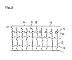
- Figs. 2(a) ~ (e) are representations explaing technique for forming molecular wirings by use of the Fig. 1 technique; and
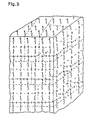
- Figs. 3 shows a configuration of a molecular controlled structure according to the invention.
- In the following, embodiments of this invention are described with reference to Figs. 1 ~ 3.
- A first embodiment of this invention is described with reference to Fig. 1. On a
Si substrate 10 formed with SiO2, there is formed by chemical adsorption process, amonomolecular film 12 of
bonding 14 of at the Si02 surface [FIG. l(a)].
- Now, the
vinyl groups 16 of the silane surface active agent are juxtaposed on the surface ofsubstrate 10. - Then,
electron beams 18, which is converged to about 50Å in diameter, is used as energy beams and are irradiated onto the surface in a pattern underH 20 atmosphere of about 10-3~10-4 ofH 20 so that active groups, i.e.,-OH groups 20 are added to a part of thevinyl groups 16 in accordance with the irradiation pattern [FIG. l(b)]. - Thereafter, silane surface active agent (CH2= CH-(CH2)n-SiCℓ3) 22 is added to active group portion which has -
OH group 20 by use of the similar technique to the above stated, so that thebonding 24 of is formed [FIG. l(c)]. -

- That is, by the above-stated process, a
molecule film 26 of
vinyl groups 28 are juxtaposed and form a film. - By the repetition of the pattern irradiation of the energy beams, and the adding reaction of silane i surface active agent, a molecular controlled structure is produced in such manner that molecules are juxtaposed regularly in a three dimensional direction.
- In the above-stated embodiment, normal chain type hydrocarbon which has CH2 = CH- groups at one end of molecules and has -SiCℓ3 groups at the other end of molecules (silane surface active agent) is used. If functional groups, for example, diacetylene, pyrrole, chenylene, phenylene etc. are inserted between -CH2-CH2- bondings of normal chain type hydrocarbon or added instead of H, conjugated double bondings which shows electric conductivity at the level of molecule can be formed and it is possible to control the forming of wiring of organic molecules which is necessary for production of molecular devices at the level of molecule.
- For example, as shown in FIG. 2(a),
diacetylene group 30 is inserted between -CH2-CH2-. After a molecular controlled structure is formed, deep UV is irradiated therewith so that molecular wiring of poly-diacetylene 32 [FIG. 2(b)] can be formed in a direction which is desired in the same plane. - In case that electric conductivity is needed in a vertical direction, molecules, in each of which insertion position of poly-diacetylene into normal chain hydrocarbon portion is shifted every 3 carbon atoms.
- Further, as shown in FIGS. 2(c) ~ (e),
molecules 34 includingphenyl group 36 instead of the above-stated diacetylene group can be added by the irradiation ofelectron beams 18 at the side position of poly-diacetylene forming layer 40, thereby molecules having phenyl group are regularly formed as alayer 42, in adjacent to thelayer 40 of molecules having diacetylene group. - When CH≡CH- group is used instead of CH2 =CH- group and -NH2 group is used instead of -SiCℓ3 group, the same advantages as stated above may be obtained.
- In another method, cyanobromide (CNBr) is added to -OH group 6 as shown in the following formula (3) to thereby be cyanized.

- Thereafter, amino group is reacted thereto so that monomolecule can be selectively added. [cyanobromide technique].
- As still another method, there is a method in which amino group is added by use of end epoxy group as shown in the following formula (4) [epoxy technique].
- As one example, there is a case that CH≡CH-(CH2)n-NH2 is selectively added. In this case, -OH group 6 of -(CH2)n-OH, which is formed in the same manner as shown in FIG. l(b), is oxidized by periodic acid (HI04) to thereby be aldehyded as shown in the following formula (1).
-

- Thereafter, it is selectively reacted with -NH2 group which is then added thereto as shown in the following formula (2). [aldehyde technique]

- Further, adding reaction by use of reaction between end thiol group (R-SH) and


- In the forgoing embodiments, if diameter of electron beam is made smaller (e.g., about 5A), it becomes necessarily possible to produce a molecular controlled structure by controlling each molecule one by one.
- It is also possible to form molecules with regularity at a desired portion by controlling plural kinds of molecules. For example, it is possible to produce a molecular controlled structure shown in FIG. 3. In FIG. 3, A, B, C represent different functional groups, respectively. The molecules having 3 kinds of functional groups are formed regularly in 3 (i.e., vertical, horizontal, hight) directions.
- While specific embodiments of the invention have been illustrated and described herein, it is realized that modifications and changes will occurr to those skilled in the art. It is therefore to be understood that the appended claims are intended to cover all modifications and changes as fall within the true spirit and scope of the invention.
Claims (9)
- . A molecular controlled structure comprising:a plurality of normal chain hydrocarbon molecules, each having at one end thereof energy responsive group and having at the other end thereof reaction group which reacts said responsive group or induced group from said responsive group,at least some of said normal chain hydrocarbon molecules having functional group which responds to light, electron beam, X-ray, r-ray, heat, electron, or ion, said molecules being bonded in three dimensional configuration.
- 2. The molecular controlled structure of claim 1, wherein said energy responsive group includes double bonding of C=C or carbons, and said reaction group includes Si.
- 3. The molucular controlled structure of claim 1, wherein said functional group includes conjugated double bonding or group which forms conjugated double bonding in the course of production of said molecular controlled structure.
- 4. A molecular controlled structure comprising:a plurality of normal chain hydrocarbon molecules, each having at one end thereof energy responsive group and.having at the other end thereof reaction group which reacts said responsive group or induced group from said responsive group , said energy responsive group including double bonding of C=C or carbons, and said reaction group including Si,at least some of said normal chain hydrocarbon molecules having functional group which responds to light, electron beam, X-ray, r-ray, heat, electron or ion, said functional group including conjugated double bonding or group which forms conjugated double bonding in the course of production of said molecular controlled structure, and said molecules being bonded in three dimensional configuration.
- 5. A method of producing a molecular controlled structure comprising the steps of:forming a thin film which includes responsive group producing chemical reaction due to irradiation of energy beam on a substrate;selectively activating said responsive group by irradiating energy beams with said thin film in a pattern in gaseous atmosphere or in liquid; andselectively connecting chemical substance on said activated portion.
- 6. The method of claim 5, wherein, as said chemical substance, a molecule having reaction group to be reacted with said responsive group activated at one end and having another responsive group which functions in the same manner as said responsive group at the other end is used.
- 7. The method of claim 5, wherein monomolecular thin film is formed by Langmuir Brodgett technique or absorption technique in such manner that responsive group are exposed and juxtaposed on the surface of substrate in said step of forming the thin film.
- 8. The method of claim 5, wherein said chemical substance includes -NH2group, -SH group, C=CH group.
- 9. The method of claim 5, wherein said chemical substance includes -NH group, -SH group, -C=C group.
Applications Claiming Priority (2)
| Application Number | Priority Date | Filing Date | Title |
|---|---|---|---|
| JP216649/84 | 1984-10-16 | ||
| JP59216649A JPS6194042A (en) | 1984-10-16 | 1984-10-16 | Molecular construction and its manufacture |
Publications (3)
| Publication Number | Publication Date |
|---|---|
| EP0178606A2 true EP0178606A2 (en) | 1986-04-23 |
| EP0178606A3 EP0178606A3 (en) | 1987-09-02 |
| EP0178606B1 EP0178606B1 (en) | 1992-01-15 |
Family
ID=16691752
Family Applications (1)
| Application Number | Title | Priority Date | Filing Date |
|---|---|---|---|
| EP85112928A Expired EP0178606B1 (en) | 1984-10-16 | 1985-10-11 | Molecular controlled structure and method of manufacturing the same |
Country Status (4)
| Country | Link |
|---|---|
| US (1) | US4673474A (en) |
| EP (1) | EP0178606B1 (en) |
| JP (1) | JPS6194042A (en) |
| DE (1) | DE3585198D1 (en) |
Cited By (6)
| Publication number | Priority date | Publication date | Assignee | Title |
|---|---|---|---|---|
| EP0291659A1 (en) * | 1987-03-24 | 1988-11-23 | Matsushita Electric Industrial Co., Ltd. | Molecular electronic element |
| EP0299366A2 (en) * | 1987-07-16 | 1989-01-18 | BASF Aktiengesellschaft | Method for the modification and addressing of organic films in the molecular field |
| EP0312100A2 (en) * | 1987-10-16 | 1989-04-19 | Matsushita Electric Industrial Co., Ltd. | Process for producing a polyacetylene or polydiacetylene film |
| EP0383584A2 (en) * | 1989-02-15 | 1990-08-22 | Matsushita Electric Industrial Co., Ltd. | Organic electro-conductive thin films and process for production thereof |
| US5260115A (en) * | 1989-02-15 | 1993-11-09 | Matsushita Electric Industrial Co., Ltd. | Organic electro-conductive thin films and process for production thereof |
| EP0584891A2 (en) * | 1988-06-28 | 1994-03-02 | Matsushita Electric Industrial Co., Ltd. | Method for the formation of built-up films of monomolecular layers using silane compounds having an acetylene bond |
Families Citing this family (56)
| Publication number | Priority date | Publication date | Assignee | Title |
|---|---|---|---|---|
| JPS6221151A (en) * | 1985-07-19 | 1987-01-29 | Matsushita Electric Ind Co Ltd | Formation of pattern |
| JPS6396655A (en) * | 1986-10-14 | 1988-04-27 | Matsushita Electric Ind Co Ltd | Pattern forming method |
| JPS62293242A (en) * | 1986-06-12 | 1987-12-19 | Matsushita Electric Ind Co Ltd | Method and material for forming pattern |
| JPH0774894B2 (en) * | 1987-05-25 | 1995-08-09 | コニカ株式会社 | Silver halide photographic light-sensitive material with improved sharpness |
| US5264731A (en) * | 1987-06-25 | 1993-11-23 | Matsushita Electric Industrial Co., Ltd. | Method for fabricating semiconductor device |
| JP2506973B2 (en) * | 1988-08-05 | 1996-06-12 | 松下電器産業株式会社 | Method of manufacturing optical recording medium |
| USRE38752E1 (en) * | 1990-10-25 | 2005-07-05 | Matsushita Electric Industrial Co., Ltd | Method of manufacturing a fluorocarbon-based coating film |
| US5240774A (en) * | 1990-10-25 | 1993-08-31 | Matsushita Electric Industrial Co., Ltd. | Fluorocarbon-based coating film and method of manufacturing the same |
| JP2500824B2 (en) * | 1990-10-25 | 1996-05-29 | 松下電器産業株式会社 | Fluorocarbon coating film and method for producing the same |
| EP0484746B1 (en) * | 1990-10-25 | 1996-09-18 | Matsushita Electric Industrial Co., Ltd. | Chemically adsorbed monomolecular lamination film and method of manufacturing the same |
| US5238746A (en) * | 1990-11-06 | 1993-08-24 | Matsushita Electric Industrial Co., Ltd. | Fluorocarbon-based polymer lamination coating film and method of manufacturing the same |
| DE69129145T2 (en) | 1990-12-25 | 1998-07-16 | Matsushita Electric Ind Co Ltd | Transparent substrate with applied monomolecular film and process for its production |
| US6503567B2 (en) | 1990-12-25 | 2003-01-07 | Matsushita Electric Industrial Co., Ltd. | Transparent substrate and method of manufacturing the same |
| JP2622316B2 (en) * | 1991-06-04 | 1997-06-18 | 松下電器産業株式会社 | Water / oil repellent film and method for producing the same |
| CA2060294C (en) * | 1991-02-06 | 2000-01-18 | Kazufumi Ogawa | Chemically absorbed film and method of manufacturing the same |
| EP0508136B1 (en) * | 1991-03-14 | 1998-06-03 | Matsushita Electric Industrial Co., Ltd. | Surface-treated apparel material |
| DE69227536T2 (en) * | 1991-04-30 | 1999-04-08 | Matsushita Electric Ind Co Ltd | Antistatic film and manufacturing method |
| US5652059A (en) * | 1991-11-20 | 1997-07-29 | Bar Ilan University | Method for attaching microspheres to a substrate |
| JP3140189B2 (en) * | 1992-07-29 | 2001-03-05 | 松下電器産業株式会社 | Lubricating film and manufacturing method thereof |
| EP0582131B1 (en) * | 1992-07-29 | 1997-05-02 | Matsushita Electric Industrial Co., Ltd. | Lubricating film and method of manufacturing the same |
| EP1194960B1 (en) | 1999-07-02 | 2010-09-15 | President and Fellows of Harvard College | Nanoscopic wire-based devices, arrays, and methods of their manufacture |
| US20060175601A1 (en) * | 2000-08-22 | 2006-08-10 | President And Fellows Of Harvard College | Nanoscale wires and related devices |
| US7301199B2 (en) | 2000-08-22 | 2007-11-27 | President And Fellows Of Harvard College | Nanoscale wires and related devices |
| EP2360298A3 (en) * | 2000-08-22 | 2011-10-05 | President and Fellows of Harvard College | Method for depositing a semiconductor nanowire |
| KR100991573B1 (en) * | 2000-12-11 | 2010-11-04 | 프레지던트 앤드 펠로우즈 오브 하버드 칼리지 | Nanosensors |
| US6919592B2 (en) * | 2001-07-25 | 2005-07-19 | Nantero, Inc. | Electromechanical memory array using nanotube ribbons and method for making same |
| US7259410B2 (en) | 2001-07-25 | 2007-08-21 | Nantero, Inc. | Devices having horizontally-disposed nanofabric articles and methods of making the same |
| US7566478B2 (en) | 2001-07-25 | 2009-07-28 | Nantero, Inc. | Methods of making carbon nanotube films, layers, fabrics, ribbons, elements and articles |
| US6574130B2 (en) * | 2001-07-25 | 2003-06-03 | Nantero, Inc. | Hybrid circuit having nanotube electromechanical memory |
| US6706402B2 (en) | 2001-07-25 | 2004-03-16 | Nantero, Inc. | Nanotube films and articles |
| US6643165B2 (en) | 2001-07-25 | 2003-11-04 | Nantero, Inc. | Electromechanical memory having cell selection circuitry constructed with nanotube technology |
| US6911682B2 (en) | 2001-12-28 | 2005-06-28 | Nantero, Inc. | Electromechanical three-trace junction devices |
| US6835591B2 (en) | 2001-07-25 | 2004-12-28 | Nantero, Inc. | Methods of nanotube films and articles |
| US6924538B2 (en) | 2001-07-25 | 2005-08-02 | Nantero, Inc. | Devices having vertically-disposed nanofabric articles and methods of making the same |
| US6784028B2 (en) | 2001-12-28 | 2004-08-31 | Nantero, Inc. | Methods of making electromechanical three-trace junction devices |
| US7176505B2 (en) * | 2001-12-28 | 2007-02-13 | Nantero, Inc. | Electromechanical three-trace junction devices |
| US7335395B2 (en) | 2002-04-23 | 2008-02-26 | Nantero, Inc. | Methods of using pre-formed nanotubes to make carbon nanotube films, layers, fabrics, ribbons, elements and articles |
| AU2003261205A1 (en) | 2002-07-19 | 2004-02-09 | President And Fellows Of Harvard College | Nanoscale coherent optical components |
| US7560136B2 (en) | 2003-01-13 | 2009-07-14 | Nantero, Inc. | Methods of using thin metal layers to make carbon nanotube films, layers, fabrics, ribbons, elements and articles |
| US7910064B2 (en) * | 2003-06-03 | 2011-03-22 | Nanosys, Inc. | Nanowire-based sensor configurations |
| US7658975B2 (en) * | 2003-12-12 | 2010-02-09 | Intel Corporation | Sealing porous dielectric materials |
| US20090227107A9 (en) * | 2004-02-13 | 2009-09-10 | President And Fellows Of Havard College | Nanostructures Containing Metal Semiconductor Compounds |
| US20070264623A1 (en) * | 2004-06-15 | 2007-11-15 | President And Fellows Of Harvard College | Nanosensors |
| EP1831973A2 (en) * | 2004-12-06 | 2007-09-12 | The President and Fellows of Harvard College | Nanoscale wire-based data storage |
| US20100227382A1 (en) * | 2005-05-25 | 2010-09-09 | President And Fellows Of Harvard College | Nanoscale sensors |
| WO2006132659A2 (en) * | 2005-06-06 | 2006-12-14 | President And Fellows Of Harvard College | Nanowire heterostructures |
| WO2008051316A2 (en) | 2006-06-12 | 2008-05-02 | President And Fellows Of Harvard College | Nanosensors and related technologies |
| US8058640B2 (en) | 2006-09-11 | 2011-11-15 | President And Fellows Of Harvard College | Branched nanoscale wires |
| JP5009993B2 (en) | 2006-11-09 | 2012-08-29 | ナノシス・インク. | Nanowire arrangement method and deposition method |
| WO2008127314A1 (en) | 2006-11-22 | 2008-10-23 | President And Fellows Of Harvard College | High-sensitivity nanoscale wire sensors |
| US7892610B2 (en) * | 2007-05-07 | 2011-02-22 | Nanosys, Inc. | Method and system for printing aligned nanowires and other electrical devices |
| JP2009158691A (en) * | 2007-12-26 | 2009-07-16 | Sharp Corp | Organic device and manufacturing method thereof |
| JP2012528020A (en) | 2009-05-26 | 2012-11-12 | ナノシス・インク. | Methods and systems for electric field deposition of nanowires and other devices |
| US9297796B2 (en) | 2009-09-24 | 2016-03-29 | President And Fellows Of Harvard College | Bent nanowires and related probing of species |
| EP2499276A4 (en) * | 2009-11-10 | 2013-10-02 | Univ Brigham Young | Multilayer growth by gas phase deposition |
| US10538844B2 (en) * | 2015-09-11 | 2020-01-21 | Fei Company | Nanofabrication using a new class of electron beam induced surface processing techniques |
Family Cites Families (10)
| Publication number | Priority date | Publication date | Assignee | Title |
|---|---|---|---|---|
| US2959569A (en) * | 1956-07-05 | 1960-11-08 | Dow Corning | Method of preparing organosilicon graft polymers |
| US3305524A (en) * | 1962-11-27 | 1967-02-21 | Gen Electric | Polysiloxanes |
| US3573334A (en) * | 1964-04-02 | 1971-03-30 | Union Carbide Corp | Olefinic silicone-organic polymer graft copolymers |
| US4188273A (en) * | 1973-11-22 | 1980-02-12 | Sumitomo Chemical Company, Limited | Process for preparing novel thin films |
| JPS6056285B2 (en) * | 1977-04-28 | 1985-12-09 | 凸版印刷株式会社 | How to create a resist film |
| JPS5642229A (en) * | 1979-06-25 | 1981-04-20 | University Patents Inc | New photooresist composition |
| JPS58111029A (en) * | 1981-12-24 | 1983-07-01 | Kureha Chem Ind Co Ltd | Manufacture of built-up film of diacetylene compound |
| JPS58112078A (en) * | 1981-12-26 | 1983-07-04 | Daikin Ind Ltd | Method of forming film of fluoroalkyl acrylate polymer on surface of base body |
| JPS59148335A (en) * | 1983-02-14 | 1984-08-25 | Nippon Telegr & Teleph Corp <Ntt> | Forming method of minute pattern |
| US4597999A (en) * | 1984-10-04 | 1986-07-01 | The Hospital For Sick Children | Method for coupling a hydrocarbon containing molecular species |
-
1984
- 1984-10-16 JP JP59216649A patent/JPS6194042A/en not_active Expired - Lifetime
-
1985
- 1985-10-11 DE DE8585112928T patent/DE3585198D1/en not_active Expired - Lifetime
- 1985-10-11 EP EP85112928A patent/EP0178606B1/en not_active Expired
- 1985-10-15 US US06/787,368 patent/US4673474A/en not_active Expired - Lifetime
Non-Patent Citations (1)
| Title |
|---|
| JOURNAL OF THE AMERICAN CHEMICAL SOCIETY, vol. 105, no. 1, 12th January 1983, pages 674-676, Gaston, US; L.NETZER et al.: "A new approach to construction of artificial monolayer assemblies" * |
Cited By (13)
| Publication number | Priority date | Publication date | Assignee | Title |
|---|---|---|---|---|
| US5035835A (en) * | 1987-03-24 | 1991-07-30 | Matsushita Electric Industrial Co., Ltd. | Modulatory molecular element |
| EP0291659A1 (en) * | 1987-03-24 | 1988-11-23 | Matsushita Electric Industrial Co., Ltd. | Molecular electronic element |
| EP0299366A2 (en) * | 1987-07-16 | 1989-01-18 | BASF Aktiengesellschaft | Method for the modification and addressing of organic films in the molecular field |
| EP0299366A3 (en) * | 1987-07-16 | 1991-10-23 | BASF Aktiengesellschaft | Method for the modification and addressing of organic films in the molecular field |
| EP0312100A3 (en) * | 1987-10-16 | 1989-07-26 | Matsushita Electric Industrial Co., Ltd. | Process for producing a polyacetylene |
| US4968524A (en) * | 1987-10-16 | 1990-11-06 | Matsushita Electric Industrial Co., Ltd. | Process for producing a polyacetylene |
| EP0312100A2 (en) * | 1987-10-16 | 1989-04-19 | Matsushita Electric Industrial Co., Ltd. | Process for producing a polyacetylene or polydiacetylene film |
| EP0584891A2 (en) * | 1988-06-28 | 1994-03-02 | Matsushita Electric Industrial Co., Ltd. | Method for the formation of built-up films of monomolecular layers using silane compounds having an acetylene bond |
| EP0584891A3 (en) * | 1988-06-28 | 1994-08-17 | Matsushita Electric Ind Co Ltd | Method for the formation of monomolecular adsorption films or built-up films of monomolecular layers using silane compounds having an acetylene or diacetylene bond |
| EP0383584A2 (en) * | 1989-02-15 | 1990-08-22 | Matsushita Electric Industrial Co., Ltd. | Organic electro-conductive thin films and process for production thereof |
| EP0383584A3 (en) * | 1989-02-15 | 1991-12-04 | Matsushita Electric Industrial Co., Ltd. | Organic electro-conductive thin films and process for production thereof |
| US5116638A (en) * | 1989-02-15 | 1992-05-26 | Matsushita Electric Industrial Co., Ltd. | Organic electro-conductive thin films and process for production thereof |
| US5260115A (en) * | 1989-02-15 | 1993-11-09 | Matsushita Electric Industrial Co., Ltd. | Organic electro-conductive thin films and process for production thereof |
Also Published As
| Publication number | Publication date |
|---|---|
| US4673474A (en) | 1987-06-16 |
| DE3585198D1 (en) | 1992-02-27 |
| EP0178606A3 (en) | 1987-09-02 |
| JPS6194042A (en) | 1986-05-12 |
| EP0178606B1 (en) | 1992-01-15 |
Similar Documents
| Publication | Publication Date | Title |
|---|---|---|
| EP0178606A2 (en) | Molecular controlled structure and method of manufacturing the same | |
| Bertilsson et al. | Infrared study of thiol monolayer assemblies on gold: preparation, characterization, and functionalization of mixed monolayers | |
| US5635246A (en) | Chemically adsorbed film and method of manufacturing the same | |
| US5057339A (en) | Metallized polyacetylene-type or polyacene-type ultralong conjugated polymers and process for producing the same | |
| Gardner et al. | Systems for orthogonal self-assembly of electroactive monolayers on Au and ITO: an approach to molecular electronics | |
| CA2054094A1 (en) | Chemically adsorbed monomolecular lamination film | |
| US5548117A (en) | Probe for a scanning tunneling microscope and method of manufacturing a probe | |
| US5011518A (en) | Permselective membrane and process for producing the same | |
| US5017975A (en) | Organic electronic device with a monomolecular layer or multi-monomolecular layer having electroconductive conjugated bonds | |
| US5102798A (en) | Surface functionalized Langmuir-Blodgett films for immobilization of active moieties | |
| KR940004732A (en) | Pattern formation method and thin film formation method used for pattern formation | |
| CN100377795C (en) | Conjugated molecular assembly, method of fabricating the assembly and device including the assembly | |
| US5436033A (en) | Method of manufacturing a polymer ultra thin film electret | |
| US5093154A (en) | Process for preparing a monomolecular built-up film | |
| US5277980A (en) | Mass of fine particles of inorganic material and a film of the fine inorganic particles | |
| Tang et al. | Self-assembled monolayer of polyoxometalate on gold surfaces: quartz crystal microbalance, electrochemistry, and in-situ scanning tunneling microscopy study | |
| EP0511657B1 (en) | Hydrophilic chemically adsorbed film and method of manufacturing the same | |
| EP0312100B1 (en) | Process for producing a polyacetylene or polydiacetylene film | |
| US5695836A (en) | Antistatic film and method of manufacturing the same | |
| Mao et al. | Polymer immobilization to alkylchlorosilane organic monolayer films using sequential derivatization reactions | |
| US5246740A (en) | Process for preparing a lamination of organic monomolecular films, and a chemical adsorbent used for the process | |
| US11666941B2 (en) | Methods of nanoscale directional wetting and uses thereof | |
| US5304582A (en) | Process for producing polyacetylene or polyacene type long conjugated polymers | |
| US5304583A (en) | Process for producing polyacetylene or polyacene type long conjugated polymers | |
| US5248526A (en) | Process for producing polyacetylene or polyacene type long conjugated polymers |
Legal Events
| Date | Code | Title | Description |
|---|---|---|---|
| PUAI | Public reference made under article 153(3) epc to a published international application that has entered the european phase |
Free format text: ORIGINAL CODE: 0009012 |
|
| AK | Designated contracting states |
Kind code of ref document: A2 Designated state(s): DE FR GB |
|
| PUAL | Search report despatched |
Free format text: ORIGINAL CODE: 0009013 |
|
| AK | Designated contracting states |
Kind code of ref document: A3 Designated state(s): DE FR GB |
|
| 16A | New documents despatched to applicant after publication of the search report | ||
| 17P | Request for examination filed |
Effective date: 19871006 |
|
| 17Q | First examination report despatched |
Effective date: 19890220 |
|
| GRAA | (expected) grant |
Free format text: ORIGINAL CODE: 0009210 |
|
| AK | Designated contracting states |
Kind code of ref document: B1 Designated state(s): DE FR GB |
|
| REF | Corresponds to: |
Ref document number: 3585198 Country of ref document: DE Date of ref document: 19920227 |
|
| ET | Fr: translation filed | ||
| PLBE | No opposition filed within time limit |
Free format text: ORIGINAL CODE: 0009261 |
|
| STAA | Information on the status of an ep patent application or granted ep patent |
Free format text: STATUS: NO OPPOSITION FILED WITHIN TIME LIMIT |
|
| 26N | No opposition filed | ||
| REG | Reference to a national code |
Ref country code: GB Ref legal event code: IF02 |
|
| PGFP | Annual fee paid to national office [announced via postgrant information from national office to epo] |
Ref country code: GB Payment date: 20041006 Year of fee payment: 20 |
|
| PGFP | Annual fee paid to national office [announced via postgrant information from national office to epo] |
Ref country code: DE Payment date: 20041007 Year of fee payment: 20 |
|
| PGFP | Annual fee paid to national office [announced via postgrant information from national office to epo] |
Ref country code: FR Payment date: 20041008 Year of fee payment: 20 |
|
| PG25 | Lapsed in a contracting state [announced via postgrant information from national office to epo] |
Ref country code: GB Free format text: LAPSE BECAUSE OF EXPIRATION OF PROTECTION Effective date: 20051010 |
|
| REG | Reference to a national code |
Ref country code: GB Ref legal event code: PE20 |