EP0179401B1 - Dynamically allocated local/global storage system - Google Patents
Dynamically allocated local/global storage system Download PDFInfo
- Publication number
- EP0179401B1 EP0179401B1 EP85113174A EP85113174A EP0179401B1 EP 0179401 B1 EP0179401 B1 EP 0179401B1 EP 85113174 A EP85113174 A EP 85113174A EP 85113174 A EP85113174 A EP 85113174A EP 0179401 B1 EP0179401 B1 EP 0179401B1
- Authority
- EP
- European Patent Office
- Prior art keywords
- storage
- node
- address
- processor
- local
- Prior art date
- Legal status (The legal status is an assumption and is not a legal conclusion. Google has not performed a legal analysis and makes no representation as to the accuracy of the status listed.)
- Expired - Lifetime
Links
Images

Classifications
-
- G—PHYSICS
- G06—COMPUTING; CALCULATING OR COUNTING
- G06F—ELECTRIC DIGITAL DATA PROCESSING
- G06F12/00—Accessing, addressing or allocating within memory systems or architectures
- G06F12/02—Addressing or allocation; Relocation
-
- G—PHYSICS
- G06—COMPUTING; CALCULATING OR COUNTING
- G06F—ELECTRIC DIGITAL DATA PROCESSING
- G06F12/00—Accessing, addressing or allocating within memory systems or architectures
- G06F12/02—Addressing or allocation; Relocation
- G06F12/0223—User address space allocation, e.g. contiguous or non contiguous base addressing
- G06F12/0292—User address space allocation, e.g. contiguous or non contiguous base addressing using tables or multilevel address translation means
-
- G—PHYSICS
- G06—COMPUTING; CALCULATING OR COUNTING
- G06F—ELECTRIC DIGITAL DATA PROCESSING
- G06F12/00—Accessing, addressing or allocating within memory systems or architectures
- G06F12/02—Addressing or allocation; Relocation
- G06F12/06—Addressing a physical block of locations, e.g. base addressing, module addressing, memory dedication
- G06F12/0646—Configuration or reconfiguration
- G06F12/0692—Multiconfiguration, e.g. local and global addressing
-
- G—PHYSICS
- G06—COMPUTING; CALCULATING OR COUNTING
- G06F—ELECTRIC DIGITAL DATA PROCESSING
- G06F12/00—Accessing, addressing or allocating within memory systems or architectures
- G06F12/02—Addressing or allocation; Relocation
- G06F12/08—Addressing or allocation; Relocation in hierarchically structured memory systems, e.g. virtual memory systems
Definitions
- the present invention relates to data processor storage systems and more particularly to dynamic storage systems for multiprocessor systems.
- U.S. Patent 4,365,295 shows a multiprocessor system including a memory system in which the memory of each processor module is divided into four logical address areas.
- the memory system includes a map which translates logical addresses to physical addresses and which co-acts with the multiprocessor system to bring pages from secondary memory into primary main memory as required to implement a virtual memory system.
- This patent which describes a conventional memory mapping system, does not address the efficient access of memory by single or multiple processors including interleaving storage references by a processor and dynamically directing storage references to global or local portions of each storage module.
- U.S. Patent 4,228,496 shows a multiprocessor system including a memory system as above to implement a virtual memory system.
- this patent which describes a conventional memory mapping system, does not address the efficient access of memory by single or multiple processors including interleaving storage references by a processor and dynamically directing storage references to global or local portions each storage module.
- U.S. Patent 4,174,514 shows apparatus for performing neighbourhood transformations on data matrices for image processing and the like achieving processing speeds greater than serial processors within a economy of memory through use of a plurality of serial neighbourhood processors that simultaneously operate upon adjoining partitioned segments of a single data matrix.
- This patent shows a multiprocessor system without any provision for access by all processors to a common global storage.
- U.S. Patent 4,121,286 shows apparatus for allocating and deallocating memory space in a multiprocessor environment.
- This patent which describes a conventional memory mapping system, does not address the efficient access of memory by single or multiple processors including interleaving storage references by a processor and dynamically directing storage references to global or local portions of each storage module.
- U.S. Patent 3,916,383 shoes a resource allocation circuit selectively activating individual processors by time slice basis where a time slice has approximately the same time duration as the system storage time.
- the resource allocation circuit includes a priority network which receives real time common resource utilisation requests from the processors according to the individual processor needs, assigns a priority rating to the received request and alters in response thereto the otherwise sequential activation of the processors.
- the patent shows a system with several independent data processors within a single central processor which is not a true multiprocessor system in the usual sense.
- the present invention relates to a system having independent processors forming a multiprocessor in which a storage system is dynamically partitioned into global storage and local storage.
- US Patent 3,820,079 shows a multiprocessing computer structured in modular form around a common control and data bus. Control functions for the various modules are distributed among the modules to facilitate system flexibility.
- the patent shows a system including conventional memory mapping and interleaving. The memory mapping does not control the interleaving, the interleaving being the same over all modules for all data.
- US Patent, 3,641,505 shows a multiprocessor computing system in which a number of processing units, program storage units, variable storage units and input/output units may be selectively combined to form one or more independent data processing systems. System partitioning into more than one independent system is controlled alternatively by manual switching or program directed partitioning signals.
- This patent which describes a conventional memory mapping system, does not address the efficient access of memory by single or multiple processors including interleaving storage references by a processor and dynamically directing storage references to global or local portions each storage module.
- US Patent 3,601,812 shows a memory system for buffering several computers to a central storage unit or a computer to several small memory units and a partitioned address scheme for the efficient use thereof.
- the digits of the address are decomposed into two disjoint subsets one of which is used as a buffer memory address and the other of which is stored with data word to effect identification thereof.
- the patent deals with buffering memory data in a multiprocessor and does not show a dynamically partitioned storage system including interleaving storage references by a processor and directing dynamically storage references to global or local portions of storage.
- the present invention includes a data processing apparatus, and method therefor, comprising a plurality of processing nodes connected by a communications network, each node including a processor and a storage device, the communications network being arranged to enable any processor to address any storage device in any node, each node also including mapping means for performing translation of virtual addresses produced by the associated processor to real addresses, said apparatus being characterised by: means for dynamically partitioning the overall storage of the apparatus, as represented by all said storage devices, into a global storage accessible by a plurality of said processors, and a local storage accessible by individual processors; said partitioning means including a control table in each of said mapping means containing interleave data indicating whether the generated real address is in local or global storage, and an address convertor controlled by said interleave data for manipulating predetermined fields of said real address as specified by the interleave data to create an absolute address by performing an interleaving transformation to adapt a page of real storage into either a sequential block of addresses completely contained within a node as local storage, or
- FIG. 1 is a block diagram of a multiprocessor system according to a preferred embodiment of the present invention.
- FIG. 2 is a block diagram of a processing node according to a preferred embodiment of the present invention.
- FIG. 3 shows the physical address space of the multiprocessor, that is, the address of each word in all the memories in the multiprocessor.
- the most significant part of the address specifies the node number.
- the least significant part of the address is the offset within one of the memories.
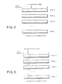
- FIG. 4 shows the entire contents of a virtual page as it would be stored with an interleave amount of zero; that is, sequentially within one of the node's memories.
- FIG. 5 shows the entire contents of a virtual page as it would be stored with an interleave amount of log base 2 of the number of nodes; that is, fully interleaved across all of the memories.
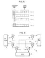
- FIG. 6 shows how an operating system would probably chose to allocate a set of sequential and interleaved pages within memory.
- FIG. 7 is a block diagram of a Map/Interleave block shown in FIG. 2 according to the present invention.
- FIG. 8 is a block diagram of a Network/Storage Interface block shown in FIG. 2 according to the present invention.
- the preferred embodiment of the present invention allows the main store of a multiple processor computer to be dynamically partitioned, at run time, between storage local to each processor and storage globally accessible by all processors.
- Some of the systems of type 2. have a fixed amount of local storage in the form of a cache to effectively reduce global storage latency; as will be noted, the present invention does not preclude the use of a cache or, in general, the use of a storage hierarchy.
- the invention described here allows the storage configuration to be dynamically altered to fit the needs of the user resulting in substantially improved performance over a wider range of applications. Efficient passing of messages between processors, achieved in systems of type 1. above by special hardware, is also supported by this invention.
- the machine organisation needed consists of N processing nodes 20 connected by some communications network 10.
- the processors and main storage of the system are contained in the nodes (see Fig. 2). Any network providing communication among all the nodes may be used.
- FIG. 1 shows an interconnection network (ICN) 10 which is connects the various nodes 20 together.
- ICN interconnection network
- This invention does not require any specific interconnection network design, but such network must necessarily have as a minimum the following capabilities: Messages which originate at any one node 20 can be reliably routed through network 10 to any other node 20.
- the routing of a message is based upon addressing information contained within a "Node #" field of the message.
- the message-routing functions of the ICN 10, when coupled with those of the various nodes 20, must enable any processor to access any memory location at any node 20 merely by specifying the correct absolute address.
- the memory-mapping mechanisms of this invention provide each processor with the capability of generating such absolute addresses.
- Fig. 2 shows the contents of a node. Addresses for storage references issued by the processor (PROC) 22 are mapped by the MAP/INTERLEAVE (M/I) 24 as described below.
- PROC processor
- M/I MAP/INTERLEAVE
- a cache 26 is used to satisfy some storage references after mapping.
- the invention described here does not require the use of a cache nor does it restrict the placement of the cache.
- the cache 26 could reside between the processor 22 and M/I block 24.
- references not satisfied by the cache 26 are directed by the network/storage interface (NET/STORE INTF. (NSI)) 28 to either the portion of main store 30 at that node or through the network 10 to store 30 of another node.
- NTI network/storage interface
- the NSI 28 also receives reference requests from other nodes and directs them to the storage of a node to be satisfied. This effectively makes the node's storage 30 dual-ported. Close to the same increase in efficiency, at lower cost, can be obtained by locally interleaving a node's storage 30 and overlapping the processing of interleaved requests.
- M/I 24 performs the usual two-level segment/page mapping of virtual addresses produced by processor 22 to real addresses, under the direction of some form of segment/page tables held in the main store 30.
- the real addresses produced uniquely identify every word or byte in all the nodes' stores: the high-order bits specify the node number, and the low-order bits specify the word or byte within a node's store. This is illustrated in Fig. 3.
- M/I 24 may also perform an interleaving transformation on the address. Whether it does so or not is specified by an additional field, unique to this invention, that is added to entries in the the segment and/or page tables. The effect of this transformation is to make a page of real storage a sequential block of addresses completely contained within a node (see Fig. 4); or a block of addresses that is scattered across several nodes' stores (see Fig. 5).
- a sequential page can thus be guaranteed to be in a node's own store 30, local to that processor 22 and quickly accessible, providing the function of a local storage. Since an interleaved page is spread across many storage blocks, the probability of storage conflicts when multiple processors reference it is greatly reduced; this provides efficient globally-accessible storage.
- the interleaving transformation may also "hash" the node number portion of the address, for example, by XOR-ing (exclusive-OR-ing) the node number portion of the address with other address bits. This would reduce the probability of conflict when regular patterns of access occur.
- the degree of interleaving used -- the number of nodes across which an interleaved page is spread -- may be specified by the additional field added to the segment and/or page tables. This field may also specify characteristics of the "hashing" used.
- part of main store 30 may be "local" and part “global.”
- the amount that is local vs. global is under control of the storage mapping tables, and thus may be changed at run time to match the requirements of applications.
- FIG. 6 An example of the kind of main store use that this invention makes possible is illustrated in Fig. 6. This shows global storage allocated from one end of all nodes' storage 30, local storage from the other. While this is not the only way of using the invention described here, it illustrates how the invention allows the proportions of storage used for global and local storage to change in the course of running applications.
- Direct main storage data movement instructions e.g., "MVCL” IBM System 370 Principles of Operation
- MVCL IBM System 370 Principles of Operation
- the storage mapping tables are used by the M/I. They define the mapping performed by the M/I between the address issued by the processor and the address accessed in memory. Specifically, and unique to this invention, they define whether an interleaving transformation is to be applied to an address or not, and may specify what interleaving transformation if any is to be applied.
- the tables themselves may reside in the M/I itself; or in the main memory of the system (either global or local storage), referenced by the M/I; or in both. Wherever they reside, they are modifiable by software running on the system's processors.
- interleaving in these tables will often be convenient to combine the definition of interleaving in these tables with a virtual memory mapping of some form, e.g., page mapping, segment mapping, or two-level segment and page mapping ((reference: Baer, J., "Computer Systems Architecture", Computer Science Press, Rockville, MD, 1980)) by extending the usual contents of such tables to include a field of at least one bit containing information determining the interleaving and/or remapping. This has been done in the preferred embodiment described here, but is not required by this invention, which only requires that the existence and/or amount of the interleave be controlled by each processor.
- a virtual memory mapping of some form, e.g., page mapping, segment mapping, or two-level segment and page mapping ((reference: Baer, J., "Computer Systems Architecture", Computer Science Press, Rockville, MD, 1980)
- processors' instruction set to have interleaved and non-interleaved data access instructions
- instruction set extension or I/O instruction control have instructions that turn interleaving on or off for data and/or instruction fetch.
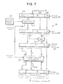
- FIG. 7 illustrates the operation of the Map/Interleave (M/I) for the case where memory mapping and low-order remapping are both incorporated.
- the top of the figure shows a virtual address as received from the processor and stored in VAR 242. This is subdivided, as shown, into a segment and/or page index (S/P I) 244, a page offset (PO) 246, and a word offset (WO) 248. These fields have the conventional meanings in memory mapping systems.
- the WO which specifies which byte in an addressed word (or word in a larger minimal unit of addressing) is to be accessed is passed through the entire mapping process unchanged (as shown), and will not be mentioned further.
- the S/P I is used in a conventional way as an index into the storage mapping tables, as shown.
- the real Segment/Page offset (S/P O) 250 is derived in a conventional way by Table Lookup to form a Real Address as shown.
- the Table Lookup also produces an interleave amount (shown) associated with each segment and/or page which is specified in the storage mapping tables.
- the low-order Remap 252 may be applied to produce a Remapped Address in RAR 254. This may also be applied as part of the variable amount variable-width right rotate described below, or may be omitted, in which case the Real Address is passed through unchanged to the next stage.
- the low-order Remap operates on a field LR to produce a new address field LR' of the same width, using the rest of the Real Address (field labelled HR) as shown.
- the width of LR (and LR') may be any value between two extremes: at largest, it is equal in width to the page offset (PO); at smallest, it is the maximum allowed interleave amount, i.e., if the width is N, the maximum number of memory modules is 2**N.
- Fig. 7 shows it at an intermediate point between these two extremes.
- the purpose of the low-order Remap is to randomise successive addresses that are to be interleaved across a subset of memory modules, i.e. accessed in different sequences. This lowers the probability of many processors accessing the same memory module simultaneously when the data structures being accessed have a size that is an integer multiple of the amount of storage in one interleaved sweep across all the memories.
- the maximum size of LR arises from the need to keep pages addressed in contiguously-addressed blocks; the minimum size is the minimum needed to effectively perform the function described above.
- the low-order Remap is one-to-one, i.e., every possible value of LR must be mapped into a different value of LR'.
- the actual interleaving transformation is then performed by a variable amount right rotate on a variable-Width bit-field device 256, producing the actual Absolute Address used to access the system's storage modules.
- This uses the Interleave Amount derived earlier, and operates on the real address after remapping (if remapping is done) excluding the word offset (WO).
- the width of the field to be rotated and the amount the field is to be rotated are specified by the interleave amount.
- the operation of the right rotate is as follows: Let HS be numbered similarly as LS above. Given an interleave amount of Q, the width of the field to be rotated is HSq-1 through LR0. The number of bit positions the field is rotated is Q.
- the final HS' field designates the processing node whose storage module contains the data to be accessed (Node #); the combined CS and LS' fields indicate the offset in that storage module where the data word is to be found (Storage Offset); and the WO field indicates which byte or sub-word is desired.
- the arrangement as described above can function with or without a private cache memory 26.
- the cache can be positioned as indicated in Figure 2 or between the processor and NI.
- the function of cache memory is to reduce memory access time for those memory accesses which occur repeatedly in time or at contiguous memory addresses.
- For cache coherence to be maintained in a multiprocessor configuration it is necessary for such a cache to have an additional capability which would not ordinarily be implemented on a uniprocessor cache. If for example one processor can read one memory location at approximately the same time that another processor is writing in the same location, it is required that neither processor satisfy such memory references in its own cache.
- This additional capability can be provided by a variety of different means, such as cross-interrogation between different cache memories, or by specifying certain memory locations to be non-cachable. Any such caching scheme (or none at all) can be applied within this context.
- NSSI Network-Storage interface
- FIG 8. The arrangement described includes a Network-Storage interface (NSI) 28 whose operation is illustrated in Figure 8.
- the routing functions of this unit are necessary for the proper functioning of this embodiment. Any hardware configuration which provides a comparable coherent set of message-routing functions could be employed instead, and its implementation should be straightforward for anyone skilled in the art.
- Such a unit is associated with each processor node, as illustrated in Figure 2.
- the function of this unit is to route messages between the associated processor, the associated memory-controller, and other processor-nodes on the network.
- the types of messages sent include, but are not limited to Load requests issued by the local processor.
- Cache-line store requests issued by the local cache, resulting from cache-misses on storage requests by the local processor.
- Load or store requests issued by other processors or caches referencing memory locations contained in the memory of the local processor node.
- Synchronisation requests (such as test-and-set, etc.) issued by the local processor, to be performed at the local memory or at remote memory locations.
- all such messages arriving at the NSI 28 must contain information sufficient to determine whether the message is to be routed to the local processor/cache 26, the local store 30, or to the interconnection network 10.
- information is contained in the "Node #" field of the memory address. If the value of the "Node #" field coincides with the number of the local node, such requests are routed to the local memory 30; otherwise they are routed to the interconnection network 10.
- the memory-mapping scheme described above ensures that the required interleaving is thereby performed.
- responses to storage requests are routed either to the local processor 22 or to the interconnection network 10, so as to return to the processor node which originated the message.
- the NSI is capable of routing messages from any of the three sources to any of the other two outputs, based on information contained in fields within the messages.
- the devices shown in the figure can operate to perform such routing as follows:
- the PE router (PE RTE) 282 receives messages from the PE 22. If the "Node #" indicates the current node, the PE RTE 282 sends the message to the local store 30 via the local memory concentrator (LM CON) 284; otherwise, it sends it to the network via the network concentrator (NET CON) 286.
- LM CON local memory concentrator
- NET CON network concentrator
- the local memory router (LM RTE) 288 receives response messages from the local store 30. If the "Node #" indicates the current node, the LM RTE 288 sends the message to the local PE 22 via the PE concentrator (PE CON) 290; otherwise, it sends it to the network via the network concentrator (NET CON) 286.
- PE CON PE concentrator
- NET CON network concentrator
- the network router (NET RTE) 292 receives messages from the network, and on the basis of the type of each message determines whether it is (a) a request from another processor for access to the local memory module; or (b) a reply from another node containing information requested by the current node from another node's local memory. In case (a), the message is sent to the local memory via the LM CON 284; otherwise, it is sent to the local PE 22 via the PE CON 290.
- the network concentrator 286 receives messages (either requests or replies) from either the PE 22, via the PE RTE 282; or the LM 30, via the LM RTE 288. It passes both to the network 10 for routing to another node based on the message's "Node #".
- the PE concentrator 290 receives reply messages from either the local store 30, via the LM RTE 288; or the network 10, via NET RTE 292. It passes them to the PE 22 (and/or cache 26).
- the local memory concentrator 284 receives request messages from either the local PE 22, via the PE RTE 282; or network 10, via NET RTE 292. It passes them to local store 30.
- routers and concentrators indicated above must communicate control information indicating when data is valid (from the router to the mul and when it can be accepted (from the concentrator to the router).
- a two-ported memory could be used instead of the LM RTE 288 and LM CON 284 devices.
Description
- The present invention relates to data processor storage systems and more particularly to dynamic storage systems for multiprocessor systems.
- The following are systems representative of the prior art.
- U.S. Patent 4,365,295 shows a multiprocessor system including a memory system in which the memory of each processor module is divided into four logical address areas. The memory system includes a map which translates logical addresses to physical addresses and which co-acts with the multiprocessor system to bring pages from secondary memory into primary main memory as required to implement a virtual memory system.
- This patent which describes a conventional memory mapping system, does not address the efficient access of memory by single or multiple processors including interleaving storage references by a processor and dynamically directing storage references to global or local portions of each storage module.
- U.S. Patent 4,228,496 shows a multiprocessor system including a memory system as above to implement a virtual memory system.
- However, this patent which describes a conventional memory mapping system, does not address the efficient access of memory by single or multiple processors including interleaving storage references by a processor and dynamically directing storage references to global or local portions each storage module.
- U.S. Patent 4,174,514 shows apparatus for performing neighbourhood transformations on data matrices for image processing and the like achieving processing speeds greater than serial processors within a economy of memory through use of a plurality of serial neighbourhood processors that simultaneously operate upon adjoining partitioned segments of a single data matrix.
- This patent shows a multiprocessor system without any provision for access by all processors to a common global storage.
- U.S. Patent 4,121,286 shows apparatus for allocating and deallocating memory space in a multiprocessor environment.
- This patent which describes a conventional memory mapping system, does not address the efficient access of memory by single or multiple processors including interleaving storage references by a processor and dynamically directing storage references to global or local portions of each storage module.
- U.S. Patent 3,916,383 shoes a resource allocation circuit selectively activating individual processors by time slice basis where a time slice has approximately the same time duration as the system storage time. The resource allocation circuit includes a priority network which receives real time common resource utilisation requests from the processors according to the individual processor needs, assigns a priority rating to the received request and alters in response thereto the otherwise sequential activation of the processors. The patent shows a system with several independent data processors within a single central processor which is not a true multiprocessor system in the usual sense.
- The present invention relates to a system having independent processors forming a multiprocessor in which a storage system is dynamically partitioned into global storage and local storage.
- US Patent 3,820,079 shows a multiprocessing computer structured in modular form around a common control and data bus. Control functions for the various modules are distributed among the modules to facilitate system flexibility. The patent shows a system including conventional memory mapping and interleaving. The memory mapping does not control the interleaving, the interleaving being the same over all modules for all data.
- US Patent, 3,641,505 shows a multiprocessor computing system in which a number of processing units, program storage units, variable storage units and input/output units may be selectively combined to form one or more independent data processing systems. System partitioning into more than one independent system is controlled alternatively by manual switching or program directed partitioning signals.
- This patent which describes a conventional memory mapping system, does not address the efficient access of memory by single or multiple processors including interleaving storage references by a processor and dynamically directing storage references to global or local portions each storage module.
- US Patent 3,601,812 shows a memory system for buffering several computers to a central storage unit or a computer to several small memory units and a partitioned address scheme for the efficient use thereof. The digits of the address are decomposed into two disjoint subsets one of which is used as a buffer memory address and the other of which is stored with data word to effect identification thereof.
- The patent deals with buffering memory data in a multiprocessor and does not show a dynamically partitioned storage system including interleaving storage references by a processor and directing dynamically storage references to global or local portions of storage.
- The prior art discussed above does not teach nor suggest the present invention as disclosed and claimed herein.
- It is an object of the present invention to partition a storage system into a global storage efficiently accessible by a plurality of processors, and local storage efficiently accessible by individual processors.
- Accordingly, the present invention includes a data processing apparatus, and method therefor, comprising a plurality of processing nodes connected by a communications network, each node including a processor and a storage device, the communications network being arranged to enable any processor to address any storage device in any node, each node also including mapping means for performing translation of virtual addresses produced by the associated processor to real addresses, said apparatus being characterised by: means for dynamically partitioning the overall storage of the apparatus, as represented by all said storage devices, into a global storage accessible by a plurality of said processors, and a local storage accessible by individual processors; said partitioning means including a control table in each of said mapping means containing interleave data indicating whether the generated real address is in local or global storage, and an address convertor controlled by said interleave data for manipulating predetermined fields of said real address as specified by the interleave data to create an absolute address by performing an interleaving transformation to adapt a page of real storage into either a sequential block of addresses completely contained within a node as local storage, or a block of addresses that is distributed across several nodes' storage devices as global storage.
- The foregoing and other objects, features and advantages of the invention will be apparent from the more particular description of the preferred embodiments of the invention, as illustrated in the accompanying drawings.
- FIG. 1 is a block diagram of a multiprocessor system according to a preferred embodiment of the present invention.
- FIG. 2 is a block diagram of a processing node according to a preferred embodiment of the present invention.
- FIG. 3 shows the physical address space of the multiprocessor, that is, the address of each word in all the memories in the multiprocessor. The most significant part of the address specifies the node number. The least significant part of the address is the offset within one of the memories.
- FIG. 4 shows the entire contents of a virtual page as it would be stored with an interleave amount of zero; that is, sequentially within one of the node's memories.
- FIG. 5 shows the entire contents of a virtual page as it would be stored with an interleave amount of
log base 2 of the number of nodes; that is, fully interleaved across all of the memories. - FIG. 6 shows how an operating system would probably chose to allocate a set of sequential and interleaved pages within memory.
- FIG. 7 is a block diagram of a Map/Interleave block shown in FIG. 2 according to the present invention.
- FIG. 8 is a block diagram of a Network/Storage Interface block shown in FIG. 2 according to the present invention.
- In the drawing, like elements are designated with similar reference numbers, and identical elements in different specific embodiments are designated by identical reference numbers.
- The preferred embodiment of the present invention allows the main store of a multiple processor computer to be dynamically partitioned, at run time, between storage local to each processor and storage globally accessible by all processors.
- Prior art multiprocessor systems provide either
- 1. only local, and no global storage
- 2. only global, and no local storage
- 3. global storage and a fixed amount of local storage
- Some of the systems of
type 2. have a fixed amount of local storage in the form of a cache to effectively reduce global storage latency; as will be noted, the present invention does not preclude the use of a cache or, in general, the use of a storage hierarchy. - Unlike the above systems, the invention described here allows the storage configuration to be dynamically altered to fit the needs of the user resulting in substantially improved performance over a wider range of applications. Efficient passing of messages between processors, achieved in systems of
type 1. above by special hardware, is also supported by this invention. - As shown in Fig. 1, the machine organisation needed consists of
N processing nodes 20 connected by somecommunications network 10. The processors and main storage of the system are contained in the nodes (see Fig. 2). Any network providing communication among all the nodes may be used. - Figure 1 shows an interconnection network (ICN) 10 which is connects the
various nodes 20 together. This invention does not require any specific interconnection network design, but such network must necessarily have as a minimum the following capabilities:
Messages which originate at any onenode 20 can be reliably routed throughnetwork 10 to anyother node 20.
- The routing of a message is based upon addressing information contained within a "Node #" field of the message.
- The message-routing functions of the
ICN 10, when coupled with those of thevarious nodes 20, must enable any processor to access any memory location at anynode 20 merely by specifying the correct absolute address. - The memory-mapping mechanisms of this invention provide each processor with the capability of generating such absolute addresses.
- Fig. 2 shows the contents of a node. Addresses for storage references issued by the processor (PROC) 22 are mapped by the MAP/INTERLEAVE (M/I) 24 as described below.
- A
cache 26 is used to satisfy some storage references after mapping. The invention described here does not require the use of a cache nor does it restrict the placement of the cache. For example thecache 26 could reside between theprocessor 22 and M/I block 24. - References not satisfied by the cache 26 (or all references, if there is no cache) are directed by the network/storage interface (NET/STORE INTF. (NSI)) 28 to either the portion of
main store 30 at that node or through thenetwork 10 to store 30 of another node. - The
NSI 28 also receives reference requests from other nodes and directs them to the storage of a node to be satisfied. This effectively makes the node'sstorage 30 dual-ported. Close to the same increase in efficiency, at lower cost, can be obtained by locally interleaving a node'sstorage 30 and overlapping the processing of interleaved requests. - M/
I 24 performs the usual two-level segment/page mapping of virtual addresses produced byprocessor 22 to real addresses, under the direction of some form of segment/page tables held in themain store 30. The real addresses produced uniquely identify every word or byte in all the nodes' stores: the high-order bits specify the node number, and the low-order bits specify the word or byte within a node's store. This is illustrated in Fig. 3. - In this invention, M/I 24 may also perform an interleaving transformation on the address. Whether it does so or not is specified by an additional field, unique to this invention, that is added to entries in the the segment and/or page tables. The effect of this transformation is to make a page of real storage a sequential block of addresses completely contained within a node (see Fig. 4); or a block of addresses that is scattered across several nodes' stores (see Fig. 5).
- A sequential page can thus be guaranteed to be in a node's
own store 30, local to thatprocessor 22 and quickly accessible, providing the function of a local storage. Since an interleaved page is spread across many storage blocks, the probability of storage conflicts when multiple processors reference it is greatly reduced; this provides efficient globally-accessible storage. - To further reduce the probability of conflicts, the interleaving transformation may also "hash" the node number portion of the address, for example, by XOR-ing (exclusive-OR-ing) the node number portion of the address with other address bits. This would reduce the probability of conflict when regular patterns of access occur.
- The degree of interleaving used -- the number of nodes across which an interleaved page is spread -- may be specified by the additional field added to the segment and/or page tables. This field may also specify characteristics of the "hashing" used.
- By having some pages mapped sequentially, and some interleaved, part of
main store 30 may be "local" and part "global." The amount that is local vs. global is under control of the storage mapping tables, and thus may be changed at run time to match the requirements of applications. - An example of the kind of main store use that this invention makes possible is illustrated in Fig. 6. This shows global storage allocated from one end of all nodes'
storage 30, local storage from the other. While this is not the only way of using the invention described here, it illustrates how the invention allows the proportions of storage used for global and local storage to change in the course of running applications. - In addition to the communication afforded by global storage, direct inter-processor message passing is supported by this invention: Direct main storage data movement instructions (e.g., "MVCL" IBM System 370 Principles of Operation) can be used to move data from a sequential page in one processor to a sequential page in another processor, without disturbing or requiring use of any other node's storage.
- The storage mapping tables are used by the M/I. They define the mapping performed by the M/I between the address issued by the processor and the address accessed in memory. Specifically, and unique to this invention, they define whether an interleaving transformation is to be applied to an address or not, and may specify what interleaving transformation if any is to be applied. The tables themselves may reside in the M/I itself; or in the main memory of the system (either global or local storage), referenced by the M/I; or in both. Wherever they reside, they are modifiable by software running on the system's processors. It will often be convenient to combine the definition of interleaving in these tables with a virtual memory mapping of some form, e.g., page mapping, segment mapping, or two-level segment and page mapping ((reference: Baer, J., "Computer Systems Architecture", Computer Science Press, Rockville, MD, 1980)) by extending the usual contents of such tables to include a field of at least one bit containing information determining the interleaving and/or remapping. This has been done in the preferred embodiment described here, but is not required by this invention, which only requires that the existence and/or amount of the interleave be controlled by each processor. Other mechanisms for doing this include: extending the processors' instruction set to have interleaved and non-interleaved data access instructions; by instruction set extension or I/O instruction control, have instructions that turn interleaving on or off for data and/or instruction fetch.
- Figure 7 illustrates the operation of the Map/Interleave (M/I) for the case where memory mapping and low-order remapping are both incorporated. The top of the figure shows a virtual address as received from the processor and stored in
VAR 242. This is subdivided, as shown, into a segment and/or page index (S/P I) 244, a page offset (PO) 246, and a word offset (WO) 248. These fields have the conventional meanings in memory mapping systems. The WO, which specifies which byte in an addressed word (or word in a larger minimal unit of addressing) is to be accessed is passed through the entire mapping process unchanged (as shown), and will not be mentioned further. - The S/P I is used in a conventional way as an index into the storage mapping tables, as shown. From the storage mapping tables, the real Segment/Page offset (S/P O) 250 is derived in a conventional way by Table Lookup to form a Real Address as shown. Unique to this invention, the Table Lookup also produces an interleave amount (shown) associated with each segment and/or page which is specified in the storage mapping tables.
- After the Real Address is derived, the low-
order Remap 252 may be applied to produce a Remapped Address inRAR 254. This may also be applied as part of the variable amount variable-width right rotate described below, or may be omitted, in which case the Real Address is passed through unchanged to the next stage. The low-order Remap operates on a field LR to produce a new address field LR' of the same width, using the rest of the Real Address (field labelled HR) as shown. The width of LR (and LR') may be any value between two extremes: at largest, it is equal in width to the page offset (PO); at smallest, it is the maximum allowed interleave amount, i.e., if the width is N, the maximum number of memory modules is 2**N. Fig. 7 shows it at an intermediate point between these two extremes. The purpose of the low-order Remap is to randomise successive addresses that are to be interleaved across a subset of memory modules, i.e. accessed in different sequences. This lowers the probability of many processors accessing the same memory module simultaneously when the data structures being accessed have a size that is an integer multiple of the amount of storage in one interleaved sweep across all the memories. The maximum size of LR arises from the need to keep pages addressed in contiguously-addressed blocks; the minimum size is the minimum needed to effectively perform the function described above. The low-order Remap is one-to-one, i.e., every possible value of LR must be mapped into a different value of LR'. One possible low-order Remap is the following: Let the bits of LR be named LR0, LR1, ... LRn from right to left; and the bits of of HR and LR' be named similarly. Then, using "xor" to represent the conventional exclusive-or logic function, a suitable low-order remap is: LR'0 = LR0 xor HR0; LR'1 = LR1 xor HR1; ... LR'n = LRn xor HRn. - The actual interleaving transformation is then performed by a variable amount right rotate on a variable-Width bit-
field device 256, producing the actual Absolute Address used to access the system's storage modules. This uses the Interleave Amount derived earlier, and operates on the real address after remapping (if remapping is done) excluding the word offset (WO). The width of the field to be rotated and the amount the field is to be rotated are specified by the interleave amount. The operation of the right rotate is as follows: Let HS be numbered similarly as LS above. Given an interleave amount of Q, the width of the field to be rotated is HSq-1 through LR0. The number of bit positions the field is rotated is Q. Instead of a variable amount variable-Width right rotate, a conventional bitwise rotation of the combined HS, CS, and LS fields by Q could be used. However, the scheme presented allows systems to be constructed with fewer than the maximum number of processing nodes because it retains, in theAbsolute Address Reg 258, high-order (leftmost) Os that appeared the Remapped Address inRAR 254. Conventional rotation would not do this, and therefore the fact that all possible values of LS must be allowed forces addressing of all possible nodes. - In the absolute address, the final HS' field designates the processing node whose storage module contains the data to be accessed (Node #); the combined CS and LS' fields indicate the offset in that storage module where the data word is to be found (Storage Offset); and the WO field indicates which byte or sub-word is desired.
- Note that when the interleave amount is 0, the variable amount Variable-Width right rotate leaves HS' equal to HS, and LS' equal to LS. This leaves the Absolute Address the same as the Remapped Address, thus providing direct sequential addressing. This provides the sequential addressing described above. Appropriate values in the Storage Mapping Tables allow this to be storage local to the node generating the addresses, or storage entirely contained in other nodes (the latter useful for message passing and other operations).
- Note also that the use of less than the maximum possible interleaving effectively restricts the processors across which global memory is allocated. This can be used in several ways, e.g.: (a) to allow the system to continue to operate, although in a degraded mode, if some of the storage modules are inoperative due to their failure, the failure of the network, etc.; (b) to effectively partition the system, allowing parts to have their own global and local memory allocation independent of other parts, thus reducing interference between those parts -- either to run several independent problems, or a well-partitioned single problem.
- The arrangement as described above can function with or without a
private cache memory 26. The cache can be positioned as indicated in Figure 2 or between the processor and NI. The function of cache memory is to reduce memory access time for those memory accesses which occur repeatedly in time or at contiguous memory addresses. For cache coherence to be maintained in a multiprocessor configuration, it is necessary for such a cache to have an additional capability which would not ordinarily be implemented on a uniprocessor cache. If for example one processor can read one memory location at approximately the same time that another processor is writing in the same location, it is required that neither processor satisfy such memory references in its own cache. This additional capability can be provided by a variety of different means, such as cross-interrogation between different cache memories, or by specifying certain memory locations to be non-cachable. Any such caching scheme (or none at all) can be applied within this context. - The arrangement described includes a Network-Storage interface (NSI) 28 whose operation is illustrated in Figure 8. The routing functions of this unit (as described below) are necessary for the proper functioning of this embodiment. Any hardware configuration which provides a comparable coherent set of message-routing functions could be employed instead, and its implementation should be straightforward for anyone skilled in the art. Such a unit is associated with each processor node, as illustrated in Figure 2. The function of this unit is to route messages between the associated processor, the associated memory-controller, and other processor-nodes on the network. The types of messages sent include, but are not limited to
Load requests issued by the local processor. - Store requests issued by the local processor.
- Cache-line load requests issued by the local cache, resulting from cache-misses on storage requests by the local processor.
- Cache-line store requests issued by the local cache, resulting from cache-misses on storage requests by the local processor.
- Responses to storage load or store requests by the local processor and/or cache.
- Load or store requests issued by other processors or caches, referencing memory locations contained in the memory of the local processor node.
- Responses to storage requests issued by other processors or caches, being returned from the memory of the local processor node.
- Messages from the local processor to remote processors, or from remote processor nodes to the local processor.
- Synchronisation requests (such as test-and-set, etc.) issued by the local processor, to be performed at the local memory or at remote memory locations.
- Responses to synchronisation requests.
- All such messages must contain information sufficient to identify the type of the message.
- In addition, all such messages arriving at the
NSI 28 must contain information sufficient to determine whether the message is to be routed to the local processor/cache 26, thelocal store 30, or to theinterconnection network 10. In the case of storage requests, by a processor or cache, such information is contained in the "Node #" field of the memory address. If the value of the "Node #" field coincides with the number of the local node, such requests are routed to thelocal memory 30; otherwise they are routed to theinterconnection network 10. The memory-mapping scheme described above ensures that the required interleaving is thereby performed. Similarly, responses to storage requests are routed either to thelocal processor 22 or to theinterconnection network 10, so as to return to the processor node which originated the message. Other messages also must contain "Node #" fields and message-type identifying codes, which uniquely identify such messages in order to be properly routed byNSI 28. The NSI is capable of routing messages from any of the three sources to any of the other two outputs, based on information contained in fields within the messages. In particular, the devices shown in the figure can operate to perform such routing as follows:
The PE router (PE RTE) 282 receives messages from thePE 22. If the "Node #" indicates the current node, thePE RTE 282 sends the message to thelocal store 30 via the local memory concentrator (LM CON) 284; otherwise, it sends it to the network via the network concentrator (NET CON) 286. - The local memory router (LM RTE) 288 receives response messages from the
local store 30. If the "Node #" indicates the current node, theLM RTE 288 sends the message to thelocal PE 22 via the PE concentrator (PE CON) 290; otherwise, it sends it to the network via the network concentrator (NET CON) 286. - The network router (NET RTE) 292 receives messages from the network, and on the basis of the type of each message determines whether it is (a) a request from another processor for access to the local memory module; or (b) a reply from another node containing information requested by the current node from another node's local memory. In case (a), the message is sent to the local memory via the
LM CON 284; otherwise, it is sent to thelocal PE 22 via thePE CON 290. - The
network concentrator 286 receives messages (either requests or replies) from either thePE 22, via thePE RTE 282; or theLM 30, via theLM RTE 288. It passes both to thenetwork 10 for routing to another node based on the message's "Node #". - The PE concentrator 290 receives reply messages from either the
local store 30, via theLM RTE 288; or thenetwork 10, viaNET RTE 292. It passes them to the PE 22 (and/or cache 26). - The
local memory concentrator 284 receives request messages from either thelocal PE 22, via thePE RTE 282; ornetwork 10, viaNET RTE 292. It passes them tolocal store 30. - In addition to paths for data communication, the routers and concentrators indicated above must communicate control information indicating when data is valid (from the router to the mul and when it can be accepted (from the concentrator to the router).
- A two-ported memory could be used instead of the
LM RTE 288 andLM CON 284 devices.
Claims (17)
- A data processing apparatus comprising a plurality of processing nodes (20) connected by a communications network (10), each node including a processor (22) and a storage device (30), the communications network being arranged to enable any processor to address any storage device in any node, each node also including mapping means for performing translation of virtual addresses produced by the associated processor to real addresses, said apparatus being characterised by:
means for dynamically partitioning the overall storage of the apparatus, as represented by all said storage devices, into a global storage accessible by a plurality of said processors, and a local storage accessible by individual processors;
said partitioning means including a control table in each of said mapping means containing interleave data indicating whether the generated real address is in local or global storage, and an address convertor (256) controlled by said interleave data for manipulating predetermined fields of said real address as specified by the interleave data to create an absolute address by performing an interleaving transformation to adapt a page of real storage into either a sequential block of addresses completely contained within a node as local storage, or a block of addresses that is distributed across several nodes' storage devices as global storage. - A data processing apparatus as claimed in Claim 1, wherein said partitioning means is responsive to inputs from the processors and effective in operation to cause the processors collectively to determine the relative magnitudes or sizes of the global and local storages and to cause each individual processor to determine, at least when a storage reference request to enter a quantity in storage is reached in operation of the processor, whether the quantity is entered in said global or said local storage.
- A data processing apparatus as claimed in Claim 1 or Claim 2, wherein the entries in the control tables each contain a field which
specifies the number, which can be zero, of other node addresses which contain locations contributing to the page required, the mapping means, when the number is other than zero, cyclically modifying the node address in response to said number whereby the locations of a distributed page are interleaved over a corresponding plurality of storage devices in other processing nodes. - A data processing apparatus as claimed in Claim 3, wherein the field also specifies the manner of cyclic node address modification.
- A data processing apparatus as claimed in Claim 3 or Claim 4, wherein said number is a power of 2, not exceeding the number of processing nodes currently connected to the communications network.
- A data processing apparatus as claimed in Claim 5, wherein said absolute address is created within said address convertor by performing a variable amount right rotation of a variable width address field corresponding to said real address.
- A data processing apparatus as claimed in any preceding claim, wherein each node is connected to the communications network via a local port and each node contains an interface mechanism which provides independent bi-directional interconnection between the processor and the storage device, the storage device and the local port, and the local port and the processor.
- A data processing apparatus as claimed in any preceding claim, further comprising means to re-map an interleaving sweep across storage devices to provide different sequences of storage device access for different successive interleaving sweeps.
- A method of operating a data processing apparatus of the type comprising a plurality of processing nodes (20) connected by a communications network (10), each node including a processor (22) and a storage device (30), the communications network being arranged to enable any processor to address any storage device in any node, each node also including mapping means for performing translation of virtual addresses produced by the associated processor to real addresses, said method being characterised in that the overall storage of the apparatus, as represented by all said storage devices, can be dynamically partitioned into a global storage accessible by a plurality of said processors, and a local storage accessible by individual processors, by the steps of;
including a control table in each of said mapping means containing interleave data indicating whether the generated real address is in local or global storage;
manipulating predetermined fields of said real address as specified by the interleave data to create an absolute address by performing an interleaving transformation to adapt a page of real storage into either a sequential block of addresses completely contained within a node as local storage, or a block of addresses that is distributed across several nodes' storage devices as global storage. - A method as claimed in Claim 9, wherein the step of dynamically partitioning the overall storage is responsive to inputs from the processors and is effective in operation to cause the processors collectively to determine the relative magnitudes or sizes of the global and local storages and to cause each individual processor to determine, at least when a storage reference request to enter a quantity in storage is reached in operation of the processor, whether the quantity is entered in said global or said local storage.
- A method as claimed in Claim 9 or Claim 10, further comprising the step of:
entering into the control tables a field which specifies the number, which can be zero, of other node addresses which contain locations contributing to the page required, the mapping means being responsive to this field such that, when the number is other than zero, the mapping means cyclically modifies the node address in response to said number whereby the locations of a distributed page are interleaved over a corresponding plurality of storage devices in other processing nodes. - A method as claimed in Claim 11, wherein the field also specifies the manner of cyclic node address modification.
- A method as claimed in Claim 11 or Claim 12, wherein said number is a power of 2, not exceeding the number of processing nodes currently connected to the communications network.
- A method as claimed in Claim 13, wherein said absolute address is created within said address convertor by performing a variable amount right rotation of a variable width address field corresponding to said real address.
- A method as claimed in any of claims 9 to 14, further comprising the steps of:
connecting each node to the communications network via a local port; and
providing each node with an interface mechanism which provides independent bi-directional interconnection between the processor and the storage device, the storage device and the local port, and the local port and the processor. - A method as claimed in any of claims 9 to 15, further comprising the step of re-mapping an interleaving sweep across storage devices to provide different sequences of storage device access for different successive interleaving sweeps.
- A method as claimed in any of claims 9 to 16 comprising the step of allocating storage on page boundaries, and dynamically allocating storage on variable segment boundaries.
Applications Claiming Priority (2)
| Application Number | Priority Date | Filing Date | Title |
|---|---|---|---|
| US06/664,131 US4754394A (en) | 1984-10-24 | 1984-10-24 | Multiprocessing system having dynamically allocated local/global storage and including interleaving transformation circuit for transforming real addresses to corresponding absolute address of the storage |
| US664131 | 1996-06-14 |
Publications (3)
| Publication Number | Publication Date |
|---|---|
| EP0179401A2 EP0179401A2 (en) | 1986-04-30 |
| EP0179401A3 EP0179401A3 (en) | 1989-09-13 |
| EP0179401B1 true EP0179401B1 (en) | 1992-07-22 |
Family
ID=24664672
Family Applications (1)
| Application Number | Title | Priority Date | Filing Date |
|---|---|---|---|
| EP85113174A Expired - Lifetime EP0179401B1 (en) | 1984-10-24 | 1985-10-17 | Dynamically allocated local/global storage system |
Country Status (11)
| Country | Link |
|---|---|
| US (2) | US4754394A (en) |
| EP (1) | EP0179401B1 (en) |
| JP (1) | JPS61103258A (en) |
| KR (1) | KR910001736B1 (en) |
| CN (1) | CN1004307B (en) |
| CA (1) | CA1236588A (en) |
| DE (1) | DE3586389T2 (en) |
| GB (1) | GB2165975B (en) |
| HK (2) | HK23690A (en) |
| IN (1) | IN166397B (en) |
| PH (1) | PH25478A (en) |
Cited By (1)
| Publication number | Priority date | Publication date | Assignee | Title |
|---|---|---|---|---|
| KR101288152B1 (en) * | 2008-12-31 | 2013-07-19 | 인텔 코포레이션 | Processor extensions for execution of secure embedded containers |
Families Citing this family (135)
| Publication number | Priority date | Publication date | Assignee | Title |
|---|---|---|---|---|
| US4811216A (en) * | 1986-12-22 | 1989-03-07 | American Telephone And Telegraph Company | Multiprocessor memory management method |
| US5093913A (en) * | 1986-12-22 | 1992-03-03 | At&T Laboratories | Multiprocessor memory management system with the flexible features of a tightly-coupled system in a non-shared memory system |
| US5136706A (en) * | 1987-04-30 | 1992-08-04 | Texas Instruments Incorporated | Adaptive memory management system for collection of garbage in a digital computer |
| US5111389A (en) * | 1987-10-29 | 1992-05-05 | International Business Machines Corporation | Aperiodic mapping system using power-of-two stride access to interleaved devices |
| JPH063589B2 (en) * | 1987-10-29 | 1994-01-12 | インターナシヨナル・ビジネス・マシーンズ・コーポレーシヨン | Address replacement device |
| US5055999A (en) * | 1987-12-22 | 1991-10-08 | Kendall Square Research Corporation | Multiprocessor digital data processing system |
| US5226039A (en) * | 1987-12-22 | 1993-07-06 | Kendall Square Research Corporation | Packet routing switch |
| US5251308A (en) * | 1987-12-22 | 1993-10-05 | Kendall Square Research Corporation | Shared memory multiprocessor with data hiding and post-store |
| US5341483A (en) * | 1987-12-22 | 1994-08-23 | Kendall Square Research Corporation | Dynamic hierarchial associative memory |
| US5761413A (en) * | 1987-12-22 | 1998-06-02 | Sun Microsystems, Inc. | Fault containment system for multiprocessor with shared memory |
| US5276826A (en) * | 1988-01-04 | 1994-01-04 | Hewlett-Packard Company | Apparatus for transforming addresses to provide pseudo-random access to memory modules |
| JPH0291747A (en) * | 1988-09-29 | 1990-03-30 | Hitachi Ltd | Information processor |
| JPH0833799B2 (en) * | 1988-10-31 | 1996-03-29 | 富士通株式会社 | Data input / output control method |
| AU615084B2 (en) * | 1988-12-15 | 1991-09-19 | Pixar | Method and apparatus for memory routing scheme |
| US5117350A (en) * | 1988-12-15 | 1992-05-26 | Flashpoint Computer Corporation | Memory address mechanism in a distributed memory architecture |
| FR2642252A1 (en) * | 1989-01-26 | 1990-07-27 | Centre Nat Rech Scient | Circuit interconnection unit, especially of the crossbar type, process for employing a circuit interconnection unit and uses of a circuit interconnection unit |
| IT1228728B (en) * | 1989-03-15 | 1991-07-03 | Bull Hn Information Syst | MULTIPROCESSOR SYSTEM WITH GLOBAL DATA REPLICATION AND TWO LEVELS OF ADDRESS TRANSLATION UNIT. |
| EP0389151A3 (en) * | 1989-03-22 | 1992-06-03 | International Business Machines Corporation | System and method for partitioned cache memory management |
| US5072369A (en) * | 1989-04-07 | 1991-12-10 | Tektronix, Inc. | Interface between buses attached with cached modules providing address space mapped cache coherent memory access with SNOOP hit memory updates |
| US5144692A (en) * | 1989-05-17 | 1992-09-01 | International Business Machines Corporation | System for controlling access by first system to portion of main memory dedicated exclusively to second system to facilitate input/output processing via first system |
| US5301327A (en) * | 1989-06-30 | 1994-04-05 | Digital Equipment Corporation | Virtual memory management for source-code development system |
| JPH03150637A (en) * | 1989-11-08 | 1991-06-27 | Oki Electric Ind Co Ltd | System for assigning register correspondingly to pipeline |
| US5715419A (en) * | 1989-12-05 | 1998-02-03 | Texas Instruments Incorporated | Data communications system with address remapping for expanded external memory access |
| US5682202A (en) * | 1989-12-08 | 1997-10-28 | Fuji Photo Film Co., Ltd. | Apparatus for recording/reproducing video data in a memory card on a cluster basis |
| JPH04505065A (en) * | 1989-12-26 | 1992-09-03 | イーストマン・コダック・カンパニー | Image processing device with disk storage similar to RAM storage |
| CA2073185A1 (en) * | 1990-01-05 | 1991-07-06 | Won S. Kim | Parallel processor memory system |
| US5161156A (en) * | 1990-02-02 | 1992-11-03 | International Business Machines Corporation | Multiprocessing packet switching connection system having provision for error correction and recovery |
| US5153595A (en) * | 1990-03-26 | 1992-10-06 | Geophysical Survey Systems, Inc. | Range information from signal distortions |
| JP2653709B2 (en) * | 1990-04-20 | 1997-09-17 | 富士写真フイルム株式会社 | Image / audio data playback device |
| JPH0418638A (en) * | 1990-05-11 | 1992-01-22 | Fujitsu Ltd | Static memory allocation processing method |
| JPH0430231A (en) * | 1990-05-25 | 1992-02-03 | Hitachi Ltd | Main storage addressing system |
| US5230051A (en) * | 1990-09-04 | 1993-07-20 | Hewlett-Packard Company | Distributed messaging system and method |
| US5265207A (en) * | 1990-10-03 | 1993-11-23 | Thinking Machines Corporation | Parallel computer system including arrangement for transferring messages from a source processor to selected ones of a plurality of destination processors and combining responses |
| JPH04246745A (en) * | 1991-02-01 | 1992-09-02 | Canon Inc | Memory access system |
| WO1992016895A1 (en) | 1991-03-18 | 1992-10-01 | Echelon Corporation | Networked variables |
| EP0576574B1 (en) | 1991-03-18 | 2001-10-31 | Echelon Corporation | Programming language structures for use in a network for communicating, sensing and controlling information |
| US6493739B1 (en) | 1993-08-24 | 2002-12-10 | Echelon Corporation | Task scheduling in an event driven environment |
| US5269013A (en) * | 1991-03-20 | 1993-12-07 | Digital Equipment Corporation | Adaptive memory management method for coupled memory multiprocessor systems |
| US5341485A (en) * | 1991-05-07 | 1994-08-23 | International Business Machines Corporation | Multiple virtual address translation per computer cycle |
| US5630098A (en) * | 1991-08-30 | 1997-05-13 | Ncr Corporation | System and method for interleaving memory addresses between memory banks based on the capacity of the memory banks |
| CA2078310A1 (en) * | 1991-09-20 | 1993-03-21 | Mark A. Kaufman | Digital processor with distributed memory system |
| CA2078312A1 (en) | 1991-09-20 | 1993-03-21 | Mark A. Kaufman | Digital data processor with improved paging |
| US5263003A (en) * | 1991-11-12 | 1993-11-16 | Allen-Bradley Company, Inc. | Flash memory circuit and method of operation |
| CA2073516A1 (en) * | 1991-11-27 | 1993-05-28 | Peter Michael Kogge | Dynamic multi-mode parallel processor array architecture computer system |
| US5434992A (en) * | 1992-09-04 | 1995-07-18 | International Business Machines Corporation | Method and means for dynamically partitioning cache into a global and data type subcache hierarchy from a real time reference trace |
| US5359730A (en) * | 1992-12-04 | 1994-10-25 | International Business Machines Corporation | Method of operating a data processing system having a dynamic software update facility |
| US5845329A (en) * | 1993-01-29 | 1998-12-01 | Sanyo Electric Co., Ltd. | Parallel computer |
| US5598568A (en) * | 1993-05-06 | 1997-01-28 | Mercury Computer Systems, Inc. | Multicomputer memory access architecture |
| JPH06348584A (en) * | 1993-06-01 | 1994-12-22 | Internatl Business Mach Corp <Ibm> | Data processing system |
| US5584042A (en) * | 1993-06-01 | 1996-12-10 | International Business Machines Corporation | Dynamic I/O data address relocation facility |
| US5638527A (en) * | 1993-07-19 | 1997-06-10 | Dell Usa, L.P. | System and method for memory mapping |
| GB9320982D0 (en) * | 1993-10-12 | 1993-12-01 | Ibm | A data processing system |
| US5583990A (en) * | 1993-12-10 | 1996-12-10 | Cray Research, Inc. | System for allocating messages between virtual channels to avoid deadlock and to optimize the amount of message traffic on each type of virtual channel |
| US5613067A (en) * | 1993-12-30 | 1997-03-18 | International Business Machines Corporation | Method and apparatus for assuring that multiple messages in a multi-node network are assured fair access to an outgoing data stream |
| JP3687990B2 (en) * | 1994-01-25 | 2005-08-24 | 株式会社日立製作所 | Memory access mechanism |
| SE515344C2 (en) * | 1994-02-08 | 2001-07-16 | Ericsson Telefon Ab L M | Distributed database system |
| US5530837A (en) * | 1994-03-28 | 1996-06-25 | Hewlett-Packard Co. | Methods and apparatus for interleaving memory transactions into an arbitrary number of banks |
| US5537635A (en) * | 1994-04-04 | 1996-07-16 | International Business Machines Corporation | Method and system for assignment of reclaim vectors in a partitioned cache with a virtual minimum partition size |
| US5907684A (en) * | 1994-06-17 | 1999-05-25 | International Business Machines Corporation | Independent channel coupled to be shared by multiple physical processing nodes with each node characterized as having its own memory, CPU and operating system image |
| US5727184A (en) * | 1994-06-27 | 1998-03-10 | Cirrus Logic, Inc. | Method and apparatus for interfacing between peripherals of multiple formats and a single system bus |
| JP2625385B2 (en) * | 1994-06-30 | 1997-07-02 | 日本電気株式会社 | Multiprocessor system |
| US5500852A (en) * | 1994-08-31 | 1996-03-19 | Echelon Corporation | Method and apparatus for network variable aliasing |
| US5812858A (en) * | 1994-09-16 | 1998-09-22 | Cirrus Logic, Inc. | Method and apparatus for providing register and interrupt compatibility between non-identical integrated circuits |
| US5685005A (en) * | 1994-10-04 | 1997-11-04 | Analog Devices, Inc. | Digital signal processor configured for multiprocessing |
| US5850522A (en) * | 1995-02-03 | 1998-12-15 | Dex Information Systems, Inc. | System for physical storage architecture providing simultaneous access to common file by storing update data in update partitions and merging desired updates into common partition |
| US6182121B1 (en) * | 1995-02-03 | 2001-01-30 | Enfish, Inc. | Method and apparatus for a physical storage architecture having an improved information storage and retrieval system for a shared file environment |
| US5860133A (en) * | 1995-12-01 | 1999-01-12 | Digital Equipment Corporation | Method for altering memory configuration and sizing memory modules while maintaining software code stream coherence |
| US6745292B1 (en) | 1995-12-08 | 2004-06-01 | Ncr Corporation | Apparatus and method for selectively allocating cache lines in a partitioned cache shared by multiprocessors |
| US5708790A (en) * | 1995-12-12 | 1998-01-13 | International Business Machines Corporation | Virtual memory mapping method and system for address translation mapping of logical memory partitions for BAT and TLB entries in a data processing system |
| US5954811A (en) * | 1996-01-25 | 1999-09-21 | Analog Devices, Inc. | Digital signal processor architecture |
| US5896543A (en) * | 1996-01-25 | 1999-04-20 | Analog Devices, Inc. | Digital signal processor architecture |
| US5892945A (en) * | 1996-03-21 | 1999-04-06 | Oracle Corporation | Method and apparatus for distributing work granules among processes based on the location of data accessed in the work granules |
| US5784697A (en) * | 1996-03-27 | 1998-07-21 | International Business Machines Corporation | Process assignment by nodal affinity in a myultiprocessor system having non-uniform memory access storage architecture |
| US5940870A (en) * | 1996-05-21 | 1999-08-17 | Industrial Technology Research Institute | Address translation for shared-memory multiprocessor clustering |
| US6134601A (en) * | 1996-06-17 | 2000-10-17 | Networks Associates, Inc. | Computer resource management system |
| US5933852A (en) * | 1996-11-07 | 1999-08-03 | Micron Electronics, Inc. | System and method for accelerated remapping of defective memory locations |
| WO1998043168A1 (en) * | 1997-03-21 | 1998-10-01 | International Business Machines Corporation | Address mapping for system memory |
| US6065045A (en) * | 1997-07-03 | 2000-05-16 | Tandem Computers Incorporated | Method and apparatus for object reference processing |
| US6002882A (en) * | 1997-11-03 | 1999-12-14 | Analog Devices, Inc. | Bidirectional communication port for digital signal processor |
| US5970232A (en) * | 1997-11-17 | 1999-10-19 | Cray Research, Inc. | Router table lookup mechanism |
| US6101181A (en) * | 1997-11-17 | 2000-08-08 | Cray Research Inc. | Virtual channel assignment in large torus systems |
| US6230252B1 (en) | 1997-11-17 | 2001-05-08 | Silicon Graphics, Inc. | Hybrid hypercube/torus architecture |
| US6085303A (en) * | 1997-11-17 | 2000-07-04 | Cray Research, Inc. | Seralized race-free virtual barrier network |
| US6061779A (en) * | 1998-01-16 | 2000-05-09 | Analog Devices, Inc. | Digital signal processor having data alignment buffer for performing unaligned data accesses |
| US6085254A (en) * | 1998-04-10 | 2000-07-04 | Telefonaktiebolaget Lm Ericsson (Publ) | Dynamic size alteration of memory files |
| US6401189B1 (en) | 1998-08-05 | 2002-06-04 | Michael J. Corinthios | General base state assignment for optimal massive parallelism |
| US6216174B1 (en) | 1998-09-29 | 2001-04-10 | Silicon Graphics, Inc. | System and method for fast barrier synchronization |
| US6275900B1 (en) | 1999-01-27 | 2001-08-14 | International Business Machines Company | Hybrid NUMA/S-COMA system and method |
| US7472215B1 (en) | 1999-03-31 | 2008-12-30 | International Business Machines Corporation | Portable computer system with thermal enhancements and multiple power modes of operation |
| US6345306B1 (en) * | 1999-05-05 | 2002-02-05 | International Business Machines Corporation | Packager apparatus and method for physically and logically packaging and distributing items in a distributed environment |
| US6549931B1 (en) | 1999-09-27 | 2003-04-15 | Oracle Corporation | Distributing workload between resources used to access data |
| US6609131B1 (en) | 1999-09-27 | 2003-08-19 | Oracle International Corporation | Parallel partition-wise joins |
| US6674720B1 (en) | 1999-09-29 | 2004-01-06 | Silicon Graphics, Inc. | Age-based network arbitration system and method |
| US6751698B1 (en) * | 1999-09-29 | 2004-06-15 | Silicon Graphics, Inc. | Multiprocessor node controller circuit and method |
| US6643754B1 (en) * | 2000-02-15 | 2003-11-04 | International Business Machines Corporation | System and method for dynamically allocating computer memory |
| US7260543B1 (en) | 2000-05-09 | 2007-08-21 | Sun Microsystems, Inc. | Automatic lease renewal with message gates in a distributed computing environment |
| US7111163B1 (en) | 2000-07-10 | 2006-09-19 | Alterwan, Inc. | Wide area network using internet with quality of service |
| DE10049498A1 (en) * | 2000-10-06 | 2002-04-11 | Philips Corp Intellectual Pty | Digital home network with distributed software system having virtual memory device for management of all storage devices within network |
| US7401161B2 (en) * | 2000-12-18 | 2008-07-15 | Sun Microsystems, Inc. | High performance storage array interconnection fabric using multiple independent paths |
| US7072976B2 (en) * | 2001-01-04 | 2006-07-04 | Sun Microsystems, Inc. | Scalable routing scheme for a multi-path interconnection fabric |
| US7007189B2 (en) * | 2001-05-07 | 2006-02-28 | Sun Microsystems, Inc. | Routing scheme using preferred paths in a multi-path interconnection fabric in a storage network |
| US20030037061A1 (en) * | 2001-05-08 | 2003-02-20 | Gautham Sastri | Data storage system for a multi-client network and method of managing such system |
| US6832301B2 (en) * | 2001-09-11 | 2004-12-14 | International Business Machines Corporation | Method for recovering memory |
| US7248585B2 (en) * | 2001-10-22 | 2007-07-24 | Sun Microsystems, Inc. | Method and apparatus for a packet classifier |
| US7124410B2 (en) * | 2002-01-09 | 2006-10-17 | International Business Machines Corporation | Distributed allocation of system hardware resources for multiprocessor systems |
| GB2419006B (en) * | 2002-04-22 | 2006-06-07 | Micron Technology Inc | Providing a register file memory with local addressing in a SIMD parallel processor |
| US7346690B1 (en) | 2002-05-07 | 2008-03-18 | Oracle International Corporation | Deferred piggybacked messaging mechanism for session reuse |
| US7797450B2 (en) * | 2002-10-04 | 2010-09-14 | Oracle International Corporation | Techniques for managing interaction of web services and applications |
| US7085897B2 (en) * | 2003-05-12 | 2006-08-01 | International Business Machines Corporation | Memory management for a symmetric multiprocessor computer system |
| US7379424B1 (en) | 2003-08-18 | 2008-05-27 | Cray Inc. | Systems and methods for routing packets in multiprocessor computer systems |
| US7921262B1 (en) | 2003-12-18 | 2011-04-05 | Symantec Operating Corporation | System and method for dynamic storage device expansion support in a storage virtualization environment |
| US7685354B1 (en) * | 2004-06-30 | 2010-03-23 | Sun Microsystems, Inc. | Multiple-core processor with flexible mapping of processor cores to cache banks |
| US7873776B2 (en) * | 2004-06-30 | 2011-01-18 | Oracle America, Inc. | Multiple-core processor with support for multiple virtual processors |
| KR100591371B1 (en) * | 2005-03-23 | 2006-06-20 | 엠텍비젼 주식회사 | Method for varying size of partitioned blocks of shared memory and portable terminal having shared memory |
| US7493400B2 (en) | 2005-05-18 | 2009-02-17 | Oracle International Corporation | Creating and dissolving affinity relationships in a cluster |
| US8037169B2 (en) * | 2005-05-18 | 2011-10-11 | Oracle International Corporation | Determining affinity in a cluster |
| US20070011557A1 (en) | 2005-07-07 | 2007-01-11 | Highdimension Ltd. | Inter-sequence permutation turbo code system and operation methods thereof |
| US7797615B2 (en) | 2005-07-07 | 2010-09-14 | Acer Incorporated | Utilizing variable-length inputs in an inter-sequence permutation turbo code system |
| US7856579B2 (en) | 2006-04-28 | 2010-12-21 | Industrial Technology Research Institute | Network for permutation or de-permutation utilized by channel coding algorithm |
| US7814065B2 (en) * | 2005-08-16 | 2010-10-12 | Oracle International Corporation | Affinity-based recovery/failover in a cluster environment |
| US9176741B2 (en) * | 2005-08-29 | 2015-11-03 | Invention Science Fund I, Llc | Method and apparatus for segmented sequential storage |
| US20160098279A1 (en) * | 2005-08-29 | 2016-04-07 | Searete Llc | Method and apparatus for segmented sequential storage |
| US8468356B2 (en) | 2008-06-30 | 2013-06-18 | Intel Corporation | Software copy protection via protected execution of applications |
| US9171044B2 (en) * | 2010-02-16 | 2015-10-27 | Oracle International Corporation | Method and system for parallelizing database requests |
| US8793429B1 (en) * | 2011-06-03 | 2014-07-29 | Western Digital Technologies, Inc. | Solid-state drive with reduced power up time |
| US9747287B1 (en) * | 2011-08-10 | 2017-08-29 | Nutanix, Inc. | Method and system for managing metadata for a virtualization environment |
| US8601473B1 (en) | 2011-08-10 | 2013-12-03 | Nutanix, Inc. | Architecture for managing I/O and storage for a virtualization environment |
| US8549518B1 (en) | 2011-08-10 | 2013-10-01 | Nutanix, Inc. | Method and system for implementing a maintenanece service for managing I/O and storage for virtualization environment |
| US9009106B1 (en) | 2011-08-10 | 2015-04-14 | Nutanix, Inc. | Method and system for implementing writable snapshots in a virtualized storage environment |
| US9652265B1 (en) | 2011-08-10 | 2017-05-16 | Nutanix, Inc. | Architecture for managing I/O and storage for a virtualization environment with multiple hypervisor types |
| US9772866B1 (en) | 2012-07-17 | 2017-09-26 | Nutanix, Inc. | Architecture for implementing a virtualization environment and appliance |
| US9268707B2 (en) | 2012-12-29 | 2016-02-23 | Intel Corporation | Low overhead paged memory runtime protection |
| US9417903B2 (en) | 2013-06-21 | 2016-08-16 | International Business Machines Corporation | Storage management for a cluster of integrated computing systems comprising integrated resource infrastructure using storage resource agents and synchronized inter-system storage priority map |
| US20170078367A1 (en) * | 2015-09-10 | 2017-03-16 | Lightfleet Corporation | Packet-flow message-distribution system |
| US20170108911A1 (en) * | 2015-10-16 | 2017-04-20 | Qualcomm Incorporated | System and method for page-by-page memory channel interleaving |
Family Cites Families (19)
| Publication number | Priority date | Publication date | Assignee | Title |
|---|---|---|---|---|
| US3820079A (en) * | 1971-11-01 | 1974-06-25 | Hewlett Packard Co | Bus oriented,modular,multiprocessing computer |
| US3796996A (en) * | 1972-10-05 | 1974-03-12 | Honeywell Inf Systems | Main memory reconfiguration |
| GB1411182A (en) * | 1973-01-04 | 1975-10-22 | Standard Telephones Cables Ltd | Data processing |
| US4228496A (en) * | 1976-09-07 | 1980-10-14 | Tandem Computers Incorporated | Multiprocessor system |
| US4174514A (en) * | 1976-11-15 | 1979-11-13 | Environmental Research Institute Of Michigan | Parallel partitioned serial neighborhood processors |
| US4149242A (en) * | 1977-05-06 | 1979-04-10 | Bell Telephone Laboratories, Incorporated | Data interface apparatus for multiple sequential processors |
| US4285040A (en) * | 1977-11-04 | 1981-08-18 | Sperry Corporation | Dual mode virtual-to-real address translation mechanism |
| US4254463A (en) * | 1978-12-14 | 1981-03-03 | Rockwell International Corporation | Data processing system with address translation |
| US4280176A (en) * | 1978-12-26 | 1981-07-21 | International Business Machines Corporation | Memory configuration, address interleaving, relocation and access control system |
| US4371929A (en) * | 1980-05-05 | 1983-02-01 | Ibm Corporation | Multiprocessor system with high density memory set architecture including partitionable cache store interface to shared disk drive memory |
| US4442484A (en) * | 1980-10-14 | 1984-04-10 | Intel Corporation | Microprocessor memory management and protection mechanism |
| US4509140A (en) * | 1980-11-10 | 1985-04-02 | Wang Laboratories, Inc. | Data transmitting link |
| US4414624A (en) * | 1980-11-19 | 1983-11-08 | The United States Of America As Represented By The Secretary Of The Navy | Multiple-microcomputer processing |
| JPS57162056A (en) * | 1981-03-31 | 1982-10-05 | Toshiba Corp | Composite computer system |
| JPS58149551A (en) * | 1982-02-27 | 1983-09-05 | Fujitsu Ltd | Storage controlling system |
| JPS58154059A (en) * | 1982-03-08 | 1983-09-13 | Omron Tateisi Electronics Co | Memory access system of parallel processing system |
| US4648035A (en) * | 1982-12-06 | 1987-03-03 | Digital Equipment Corporation | Address conversion unit for multiprocessor system |
| US4577274A (en) * | 1983-07-11 | 1986-03-18 | At&T Bell Laboratories | Demand paging scheme for a multi-ATB shared memory processing system |
| US4591975A (en) * | 1983-07-18 | 1986-05-27 | Data General Corporation | Data processing system having dual processors |
-
1984
- 1984-10-24 US US06/664,131 patent/US4754394A/en not_active Expired - Lifetime
-
1985
- 1985-08-20 PH PH32816A patent/PH25478A/en unknown
- 1985-09-20 CA CA000491267A patent/CA1236588A/en not_active Expired
- 1985-09-24 JP JP60208985A patent/JPS61103258A/en active Granted
- 1985-10-14 CN CN85107534.7A patent/CN1004307B/en not_active Expired
- 1985-10-15 KR KR1019850007590A patent/KR910001736B1/en not_active IP Right Cessation
- 1985-10-17 EP EP85113174A patent/EP0179401B1/en not_active Expired - Lifetime
- 1985-10-17 DE DE8585113174T patent/DE3586389T2/en not_active Expired - Fee Related
- 1985-10-21 GB GB08525903A patent/GB2165975B/en not_active Expired
- 1985-10-24 IN IN838/MAS/85A patent/IN166397B/en unknown
-
1988
- 1988-03-16 US US07/168,721 patent/US4980822A/en not_active Expired - Lifetime
-
1990
- 1990-03-29 HK HK236/90A patent/HK23690A/en unknown
-
1995
- 1995-06-08 HK HK89995A patent/HK89995A/en not_active IP Right Cessation
Cited By (4)
| Publication number | Priority date | Publication date | Assignee | Title |
|---|---|---|---|---|
| KR101288152B1 (en) * | 2008-12-31 | 2013-07-19 | 인텔 코포레이션 | Processor extensions for execution of secure embedded containers |
| US9086913B2 (en) | 2008-12-31 | 2015-07-21 | Intel Corporation | Processor extensions for execution of secure embedded containers |
| US9268594B2 (en) | 2008-12-31 | 2016-02-23 | Intel Corporation | Processor extensions for execution of secure embedded containers |
| US9442865B2 (en) | 2008-12-31 | 2016-09-13 | Intel Corporation | Processor extensions for execution of secure embedded containers |
Also Published As
| Publication number | Publication date |
|---|---|
| JPH0520776B2 (en) | 1993-03-22 |
| EP0179401A2 (en) | 1986-04-30 |
| GB8525903D0 (en) | 1985-11-27 |
| KR860003553A (en) | 1986-05-26 |
| CN1004307B (en) | 1989-05-24 |
| IN166397B (en) | 1990-04-28 |
| JPS61103258A (en) | 1986-05-21 |
| US4754394A (en) | 1988-06-28 |
| GB2165975B (en) | 1988-07-20 |
| GB2165975A (en) | 1986-04-23 |
| CN85107534A (en) | 1987-04-15 |
| EP0179401A3 (en) | 1989-09-13 |
| DE3586389T2 (en) | 1993-03-04 |
| DE3586389D1 (en) | 1992-08-27 |
| HK89995A (en) | 1995-06-16 |
| HK23690A (en) | 1990-04-06 |
| PH25478A (en) | 1991-07-01 |
| US4980822A (en) | 1990-12-25 |
| CA1236588A (en) | 1988-05-10 |
| KR910001736B1 (en) | 1991-03-22 |
Similar Documents
| Publication | Publication Date | Title |
|---|---|---|
| EP0179401B1 (en) | Dynamically allocated local/global storage system | |
| US5940870A (en) | Address translation for shared-memory multiprocessor clustering | |
| US4991088A (en) | Method for optimizing utilization of a cache memory | |
| US5111389A (en) | Aperiodic mapping system using power-of-two stride access to interleaved devices | |
| US5230045A (en) | Multiple address space system including address translator for receiving virtual addresses from bus and providing real addresses on the bus | |
| US3840863A (en) | Dynamic storage hierarchy system | |
| EP0737338B1 (en) | Address translation for massively parallel processing systems | |
| US5390336A (en) | C' parallel computer system having processing nodes with distributed memory with memory addresses defining unitary system address space | |
| US6185654B1 (en) | Phantom resource memory address mapping system | |
| US5581765A (en) | System for combining a global object identifier with a local object address in a single object pointer | |
| US5897664A (en) | Multiprocessor system having mapping table in each node to map global physical addresses to local physical addresses of page copies | |
| US6381668B1 (en) | Address mapping for system memory | |
| US7577816B2 (en) | Remote translation mechanism for a multinode system | |
| EP0817059B1 (en) | Auxiliary translation lookaside buffer for assisting in accessing data in remote address spaces | |
| KR100234654B1 (en) | Process assignment by nodal affinity in a multiprocessor system having non-uniform memory access storage architecture | |
| US6754776B2 (en) | Method and system for logical partitioning of cache memory structures in a partitoned computer system | |
| US5694567A (en) | Direct-mapped cache with cache locking allowing expanded contiguous memory storage by swapping one or more tag bits with one or more index bits | |
| US4758946A (en) | Page mapping system | |
| US4769770A (en) | Address conversion for a multiprocessor system having scalar and vector processors | |
| US5897660A (en) | Method for managing free physical pages that reduces trashing to improve system performance | |
| US20090089537A1 (en) | Apparatus and method for memory address translation across multiple nodes | |
| US5978888A (en) | Hardware-managed programmable associativity caching mechanism monitoring cache misses to selectively implement multiple associativity levels | |
| US6026470A (en) | Software-managed programmable associativity caching mechanism monitoring cache misses to selectively implement multiple associativity levels | |
| US6480943B1 (en) | Memory address interleaving and offset bits for cell interleaving of memory | |
| EP0745940B1 (en) | An apparatus and method for providing a cache indexing scheme less susceptible to cache collisions |
Legal Events
| Date | Code | Title | Description |
|---|---|---|---|
| PUAI | Public reference made under article 153(3) epc to a published international application that has entered the european phase |
Free format text: ORIGINAL CODE: 0009012 |
|
| AK | Designated contracting states |
Kind code of ref document: A2 Designated state(s): DE FR GB IT |
|
| 17P | Request for examination filed |
Effective date: 19860819 |
|
| PUAL | Search report despatched |
Free format text: ORIGINAL CODE: 0009013 |
|
| AK | Designated contracting states |
Kind code of ref document: A3 Designated state(s): DE FR GB IT |
|
| 17Q | First examination report despatched |
Effective date: 19910417 |
|
| GRAA | (expected) grant |
Free format text: ORIGINAL CODE: 0009210 |
|
| AK | Designated contracting states |
Kind code of ref document: B1 Designated state(s): DE FR GB IT |
|
| PG25 | Lapsed in a contracting state [announced via postgrant information from national office to epo] |
Ref country code: IT Free format text: LAPSE BECAUSE OF FAILURE TO SUBMIT A TRANSLATION OF THE DESCRIPTION OR TO PAY THE FEE WITHIN THE PRESCRIBED TIME-LIMIT;WARNING: LAPSES OF ITALIAN PATENTS WITH EFFECTIVE DATE BEFORE 2007 MAY HAVE OCCURRED AT ANY TIME BEFORE 2007. THE CORRECT EFFECTIVE DATE MAY BE DIFFERENT FROM THE ONE RECORDED. Effective date: 19920722 |
|
| REF | Corresponds to: |
Ref document number: 3586389 Country of ref document: DE Date of ref document: 19920827 |
|
| ET | Fr: translation filed | ||
| PLBE | No opposition filed within time limit |
Free format text: ORIGINAL CODE: 0009261 |
|
| STAA | Information on the status of an ep patent application or granted ep patent |
Free format text: STATUS: NO OPPOSITION FILED WITHIN TIME LIMIT |
|
| 26N | No opposition filed | ||
| PGFP | Annual fee paid to national office [announced via postgrant information from national office to epo] |
Ref country code: FR Payment date: 19951009 Year of fee payment: 11 |
|
| PGFP | Annual fee paid to national office [announced via postgrant information from national office to epo] |
Ref country code: GB Payment date: 19960925 Year of fee payment: 12 |
|
| PG25 | Lapsed in a contracting state [announced via postgrant information from national office to epo] |
Ref country code: FR Effective date: 19970630 |
|
| REG | Reference to a national code |
Ref country code: FR Ref legal event code: ST |
|
| PG25 | Lapsed in a contracting state [announced via postgrant information from national office to epo] |
Ref country code: GB Free format text: LAPSE BECAUSE OF NON-PAYMENT OF DUE FEES Effective date: 19971017 |
|
| GBPC | Gb: european patent ceased through non-payment of renewal fee |
Effective date: 19971017 |
|
| PGFP | Annual fee paid to national office [announced via postgrant information from national office to epo] |
Ref country code: DE Payment date: 19991006 Year of fee payment: 15 |
|
| PG25 | Lapsed in a contracting state [announced via postgrant information from national office to epo] |
Ref country code: DE Free format text: LAPSE BECAUSE OF NON-PAYMENT OF DUE FEES Effective date: 20010703 |