EP0180339A2 - A multi-mode radio transceiver - Google Patents
A multi-mode radio transceiver Download PDFInfo
- Publication number
- EP0180339A2 EP0180339A2 EP85307038A EP85307038A EP0180339A2 EP 0180339 A2 EP0180339 A2 EP 0180339A2 EP 85307038 A EP85307038 A EP 85307038A EP 85307038 A EP85307038 A EP 85307038A EP 0180339 A2 EP0180339 A2 EP 0180339A2
- Authority
- EP
- European Patent Office
- Prior art keywords
- signals
- balance
- radio transceiver
- quadrature
- channels
- Prior art date
- Legal status (The legal status is an assumption and is not a legal conclusion. Google has not performed a legal analysis and makes no representation as to the accuracy of the status listed.)
- Withdrawn
Links
Images


Classifications
-
- H—ELECTRICITY
- H04—ELECTRIC COMMUNICATION TECHNIQUE
- H04B—TRANSMISSION
- H04B1/00—Details of transmission systems, not covered by a single one of groups H04B3/00 - H04B13/00; Details of transmission systems not characterised by the medium used for transmission
- H04B1/38—Transceivers, i.e. devices in which transmitter and receiver form a structural unit and in which at least one part is used for functions of transmitting and receiving
- H04B1/40—Circuits
- H04B1/403—Circuits using the same oscillator for generating both the transmitter frequency and the receiver local oscillator frequency
- H04B1/406—Circuits using the same oscillator for generating both the transmitter frequency and the receiver local oscillator frequency with more than one transmission mode, e.g. analog and digital modes
-
- H—ELECTRICITY
- H03—ELECTRONIC CIRCUITRY
- H03C—MODULATION
- H03C5/00—Amplitude modulation and angle modulation produced simultaneously or at will by the same modulating signal
-
- H—ELECTRICITY
- H03—ELECTRONIC CIRCUITRY
- H03D—DEMODULATION OR TRANSFERENCE OF MODULATION FROM ONE CARRIER TO ANOTHER
- H03D1/00—Demodulation of amplitude-modulated oscillations
- H03D1/22—Homodyne or synchrodyne circuits
- H03D1/2245—Homodyne or synchrodyne circuits using two quadrature channels
-
- H—ELECTRICITY
- H03—ELECTRONIC CIRCUITRY
- H03D—DEMODULATION OR TRANSFERENCE OF MODULATION FROM ONE CARRIER TO ANOTHER
- H03D3/00—Demodulation of angle-, frequency- or phase- modulated oscillations
- H03D3/007—Demodulation of angle-, frequency- or phase- modulated oscillations by converting the oscillations into two quadrature related signals
- H03D3/008—Compensating DC offsets
-
- H—ELECTRICITY
- H03—ELECTRONIC CIRCUITRY
- H03D—DEMODULATION OR TRANSFERENCE OF MODULATION FROM ONE CARRIER TO ANOTHER
- H03D3/00—Demodulation of angle-, frequency- or phase- modulated oscillations
- H03D3/007—Demodulation of angle-, frequency- or phase- modulated oscillations by converting the oscillations into two quadrature related signals
- H03D3/009—Compensating quadrature phase or amplitude imbalances
-
- H—ELECTRICITY
- H03—ELECTRONIC CIRCUITRY
- H03D—DEMODULATION OR TRANSFERENCE OF MODULATION FROM ONE CARRIER TO ANOTHER
- H03D5/00—Circuits for demodulating amplitude-modulated or angle-modulated oscillations at will
-
- H—ELECTRICITY
- H03—ELECTRONIC CIRCUITRY
- H03D—DEMODULATION OR TRANSFERENCE OF MODULATION FROM ONE CARRIER TO ANOTHER
- H03D2200/00—Indexing scheme relating to details of demodulation or transference of modulation from one carrier to another covered by H03D
- H03D2200/0001—Circuit elements of demodulators
- H03D2200/0025—Gain control circuits
-
- H—ELECTRICITY
- H03—ELECTRONIC CIRCUITRY
- H03D—DEMODULATION OR TRANSFERENCE OF MODULATION FROM ONE CARRIER TO ANOTHER
- H03D2200/00—Indexing scheme relating to details of demodulation or transference of modulation from one carrier to another covered by H03D
- H03D2200/0001—Circuit elements of demodulators
- H03D2200/0029—Loop circuits with controlled phase shift
-
- H—ELECTRICITY
- H03—ELECTRONIC CIRCUITRY
- H03D—DEMODULATION OR TRANSFERENCE OF MODULATION FROM ONE CARRIER TO ANOTHER
- H03D2200/00—Indexing scheme relating to details of demodulation or transference of modulation from one carrier to another covered by H03D
- H03D2200/0041—Functional aspects of demodulators
- H03D2200/0047—Offset of DC voltage or frequency
-
- H—ELECTRICITY
- H03—ELECTRONIC CIRCUITRY
- H03D—DEMODULATION OR TRANSFERENCE OF MODULATION FROM ONE CARRIER TO ANOTHER
- H03D2200/00—Indexing scheme relating to details of demodulation or transference of modulation from one carrier to another covered by H03D
- H03D2200/0041—Functional aspects of demodulators
- H03D2200/005—Analog to digital conversion
-
- H—ELECTRICITY
- H03—ELECTRONIC CIRCUITRY
- H03D—DEMODULATION OR TRANSFERENCE OF MODULATION FROM ONE CARRIER TO ANOTHER
- H03D2200/00—Indexing scheme relating to details of demodulation or transference of modulation from one carrier to another covered by H03D
- H03D2200/0041—Functional aspects of demodulators
- H03D2200/0052—Digital to analog conversion
Definitions
- This invention relates to a multi-mode radio transceiver having the capability to receive and transmit signals of amplitude, frequency, phase or mixed modulation formats.
- Demodulation can then be performed in a number of ways, one of which is by using a digital signal processor (DSP) in a manner similar to that disclosed in British patent application .8127797 (J.K. Goatcher-2).
- DSP digital signal processor
- the filtered analogue quadrature signals are converted to digital signals and processed digitally to reproduce the original modulating signal according to whether the transmission modulation was am, fm or pm.
- the mixing frequency is the side band centre frequency instead of the carrier frequency.
- a multi-mode radio transceiver comprising a sequence of circuit modules characterised in that the modules are each bi-directional and include a radio frequency input/output amplifier module, a radio frequency/baseband I and Q quadrature channel conversion module, an analogue/digital conversion module, a digital signal processor, and a digital signal input/output interface, with a control means whereby for transmission a radio frequency signal is formed from analogue quadrature I and Q channel components of a digitised signal at baseband and translated to the radio transmission frequency and for reception the radio frequency signals are transformed into I and Q quadrature analogue components at baseband and subsequently digitised.
- An important feature in the successful implementation of a radio transceiver of this type is provision for automatic balancing of errors between the quadrature I and Q channels.
- Various forms of channel imbalance error can be balanced by a system of feedforward and feedback loops in the digital signal processor.
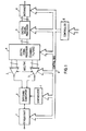
- a multi-mode radio transceiver shown in Fig. 1 there is a sequence of bi-directional circuit modules comprising a radio frequency head unit 1, a baseband converter 2, analogue/digital converters 3, a first digital signal processing stage 4, a second digital signal processing stage 5, and an interface 6.
- a frequency synthesiser 7 and a controller 8 which is linked to the modules via a control bus 9.
- reception signals are amplified (optionally) in the RF head unit and presented to the baseband converter.
- the baseband converter contains two mixers which have either their local oscillator signals or RF input signals at 90° relative phase shift.
- the resulting quadrature baseband signals are then applied to the analogue to digital converters (ADCs).
- ADCs analogue to digital converters
- the filtering may be minimal, merely protecting the RF circuitry from unwanted signals and preventing aliasing of frequencies by the ADCs.
- the digitised baseband signals are then passed to the DSPs which implement some or all of the following processes, as appropriate:
- the AGC can be used to modify the gain of the RF head unit and baseband converter and internally within the DSP to adjust the digital samples.
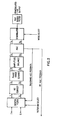
- the incoming I & Q quadrature channel signals are applied first to a digital filter 10.
- the filtered signals are then DC offset corrected (11), phase error corrected (12) and amplitude balanced (13).
- An automatic gain control (AGC) 14 is then applied before demodulation (15) is effected, e.g. in the manner disclosed in British patent application 8127797.
- the demodulated signals are passed through a post-demodulation filter 16.
- the AGC can be applied via feedback circuits, e.g. to either the digital filter 10 or possibly to the r.f. head unit 1.
- AGC can also be applied after the demodulation process, using a feed forward gain control loop. This is particularly useful when the AM demodulator according to BPA 8127797 is used. Since demodulation is a software controlled digital process the choice of demodulation mode is effected by means of a mode programme selection.
- corrections can be applied aerially or in nested loops.
- the filtered output from this detector can be directly applied as a correction signal, as shown.
- the zero crossings may be determined by zero-crossing detectors, or simple amplitude limiters may be used. In some cases it may be necessary to apply a weighting or scaling factor to the correction signal before it is used.
- the amplitude balance scheme of Figure 7 feeds an exact correction signal forward. The long term averages of rectified channel signals are divided to produce the correction factor. By halving the I-channel signal, the correction factor becomes approximately 1/2. Restricting the result of the E I/ E Q division to fractional positive numbers considerably simplifies the realisation of this loop by a digital signal processor.
- the channel imbalances need not be considered specifically as offset, phase and amplitude (or gain) terms but as any error set of the correct order.
- a long term correlation of the two channel signals will mathematically yield a correction signal of appropriate order.
- the interface provides a digital signal from which the DSPs generate baseband I- and Q-channels. These signals are converted into analogue form by the DACs.
- the mixers of the baseband converter move these signals to RF by local oscillators at 90° relative phase shift (or with 90° applied to one signal path). The addition of these two signals produces the required RF signal which is amplified (optionally) in the RF head unit.
- the AM signal is converted to RF.
- the message signal is integrated to give phase values.
- the quadrature channel signals are found from sine and cosine look up tables.
- the signals are mixed with quadrature carrier signals and summed to produce the correct FM spectrum.
- phase modulation Figure 10
- the same steps as FM are required except that the digitised message signal is used directly as the phase value for the sine and cosine look up tables.
- SSB is generated by the Weaver method which is based on quadrature channel cancellations.
- Balance corrections may be derived from a receiving measurement to estimate the imbalance on transmission (assuming reciprocity) or by feedback or feedforward loops based on the baseband converter output.
Abstract
Description
- This invention relates to a multi-mode radio transceiver having the capability to receive and transmit signals of amplitude, frequency, phase or mixed modulation formats.
- The development of radio circuits using the so-called "zero I.F." or "direct conversion" principles has enabled radio receivers to be constructed using integrated solid state circuitry, with virtually the entire r.f. portion of the receiver being incorporated in a single chip. British patent 1530602 (I.A.W. Vance-1) discloses a radio receiver structure, suitable for implementation as an integrated circuit, in which the received r.f. signals are mixed with a local oscillator signal at the carrier frequency to produce "in-phase (I)" and "quadrature (Q)" baseband signals. Demodulation can then be performed in a number of ways, one of which is by using a digital signal processor (DSP) in a manner similar to that disclosed in British patent application .8127797 (J.K. Goatcher-2). The filtered analogue quadrature signals are converted to digital signals and processed digitally to reproduce the original modulating signal according to whether the transmission modulation was am, fm or pm. In a variant on the basic direct conversion principle for single sideband modulation the mixing frequency is the side band centre frequency instead of the carrier frequency.
- According to the present invention there is provided a multi-mode radio transceiver comprising a sequence of circuit modules characterised in that the modules are each bi-directional and include a radio frequency input/output amplifier module, a radio frequency/baseband I and Q quadrature channel conversion module, an analogue/digital conversion module, a digital signal processor, and a digital signal input/output interface, with a control means whereby for transmission a radio frequency signal is formed from analogue quadrature I and Q channel components of a digitised signal at baseband and translated to the radio transmission frequency and for reception the radio frequency signals are transformed into I and Q quadrature analogue components at baseband and subsequently digitised.
- An important feature in the successful implementation of a radio transceiver of this type is provision for automatic balancing of errors between the quadrature I and Q channels. Various forms of channel imbalance error can be balanced by a system of feedforward and feedback loops in the digital signal processor.
- Embodiments of the invention will now be described with reference to the accompanying drawings, in which:
- Fig. 1 shows a block schematic diagram of a multi-mode radio transceiver,
- Fig. 2 illustrates functional elements of a digital signal processor operating in receive mode,
- Fig. 3 illustrates conversion from rectangular to polar coordinates,
- Fig. 4 illustrates a demodulation implementation,
- Figs. 5-7 illustrate various imbalance error correction arrangements,
- Figs. 8-11 illustrate various modulation arrangements.
- In the block diagram of a multi-mode radio transceiver shown in Fig. 1 there is a sequence of bi-directional circuit modules comprising a radio
frequency head unit 1, abaseband converter 2, analogue/digital converters 3, a first digitalsignal processing stage 4, a second digitalsignal processing stage 5, and aninterface 6. In addition there is a frequency synthesiser 7 and a controller 8 which is linked to the modules via a control bus 9. On reception signals are amplified (optionally) in the RF head unit and presented to the baseband converter. The baseband converter contains two mixers which have either their local oscillator signals or RF input signals at 90° relative phase shift. The resulting quadrature baseband signals are then applied to the analogue to digital converters (ADCs). Up to this point in the radio the filtering may be minimal, merely protecting the RF circuitry from unwanted signals and preventing aliasing of frequencies by the ADCs. The digitised baseband signals are then passed to the DSPs which implement some or all of the following processes, as appropriate: - i) Low pass channel filtering
- ii) Balancing of I- and Q- channels
- iii) Demodulation
- iv) Automatic gain control (AGC)
- The AGC can be used to modify the gain of the RF head unit and baseband converter and internally within the DSP to adjust the digital samples.
- In the functional breakdown of the DSPs shown in Fig. 2, for the receive mode, the incoming I & Q quadrature channel signals are applied first to a digital filter 10. The filtered signals are then DC offset corrected (11), phase error corrected (12) and amplitude balanced (13). An automatic gain control (AGC) 14 is then applied before demodulation (15) is effected, e.g. in the manner disclosed in British patent application 8127797. Finally the demodulated signals are passed through a post-demodulation filter 16. Note that the AGC can be applied via feedback circuits, e.g. to either the digital filter 10 or possibly to the r.f.
head unit 1. AGC can also be applied after the demodulation process, using a feed forward gain control loop. This is particularly useful when the AM demodulator according to BPA 8127797 is used. Since demodulation is a software controlled digital process the choice of demodulation mode is effected by means of a mode programme selection. - To demodulate the signals from the I-and Q-channels, a conversion from rectangular to polar co-ordinates is required as indicated in Figure 3. The particular modulation format is then decoded by using the amplitude (R), phase (0) or rate of change of phase information. British patent application 8127797 described a method for achieving this I-, Q-, to R, θ transformation. An alternative realisation is shown in Figure 4. This scheme has the advantage that the amplitude is found independently of phase. Thus R is not affected by phase errors and if only AM reception is required, then the demodulator can be simplified considerably. To realise either this scheme or that of application 8127797, a process equivalent to division is required. This may be carried out by finding a reciptrocal (from a look-up table) and multiplying, or by finding logarithms (from a look-up table) and subtracting. For their realisation, the other mathematical operations shown (trigonometric identities, square roots, etc.) may be found either from look-up tables or from dedicated function modules. Automatic balancing of the I- and Q- channels is necessary for satisfactory demodulation in a practical system. The correction signals can be derived by comparing long term averages of the two channels. The DC offset, departures from quadrature phasing and differences in channel gains should all be corrected. Balance can be achieved by:
- i) Feedforward of exact error correction signal
- ii) Feedback of exact error correction signal
- iii) Feedback of steps based on direction of error
- iv) Feedback of random steps (or perturbations to minimise error signal)
- Any form may be used for each correction and the corrections can be applied aerially or in nested loops.
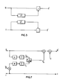
- A possible overall balance chain was shown within Figure 2. Possible detailed implementations of each balance are shown in Figures 5, 6 and 7. For DC offset, long term averaging removes all AC components and DC correction terms can be added or subtracted, as shown in Figure 5. In the phase balance scheme of Figure 6, the long term average of the product of the two channels is proportional to the phase imbalance error. Further mathematical operations on channel signals are required to find this error exactly. However, by using the sign of this error, positive or negative going steps can be generated. By applying these steps in a negative feedback loop, the channels move to a phase balance. With this scheme, a further measurement of the error magnitude (either exact or approximate), can provide a step size modulation signal giving large steps for rapid correction of big errors and small steps to minimise quantisation errors when balance is achieved. An alternative phase balance scheme is shown in 6(b). In this method, zero crossings in each channel are compared by a phase detector whose stable (zero) output occurs when there is a 90° phase difference between inputs.
- The filtered output from this detector can be directly applied as a correction signal, as shown. The zero crossings may be determined by zero-crossing detectors, or simple amplitude limiters may be used. In some cases it may be necessary to apply a weighting or scaling factor to the correction signal before it is used. The amplitude balance scheme of Figure 7 feeds an exact correction signal forward. The long term averages of rectified channel signals are divided to produce the correction factor. By halving the I-channel signal, the correction factor becomes approximately 1/2. Restricting the result of the EI/EQ division to fractional positive numbers considerably simplifies the realisation of this loop by a digital signal processor.
- Alternatively, the channel imbalances need not be considered specifically as offset, phase and amplitude (or gain) terms but as any error set of the correct order. A long term correlation of the two channel signals will mathematically yield a correction signal of appropriate order. This can be applied by a feedback or a feedforward technique. For transmission the modules of Figure 1 are used in the reverse direction to reception. The interface provides a digital signal from which the DSPs generate baseband I- and Q-channels. These signals are converted into analogue form by the DACs. The mixers of the baseband converter move these signals to RF by local oscillators at 90° relative phase shift (or with 90° applied to one signal path). The addition of these two signals produces the required RF signal which is amplified (optionally) in the RF head unit.
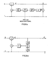
- Possible arrangements for generating amplitude, frequency, phase and SSB modulation are shown in Figures 8, 9, 10 and 11 respectively. For AM (Figure 8), only one channel is required and the other is held at zero. A DC offset is added to the digital message signal and the depth of modulation is determined by their relative levels.
- After the DAC the AM signal is converted to RF. In the FM arrangement of Figure 9, the message signal is integrated to give phase values. The quadrature channel signals are found from sine and cosine look up tables. After the DACs, the signals are mixed with quadrature carrier signals and summed to produce the correct FM spectrum. For phase modulation (Figure 10) the same steps as FM are required except that the digitised message signal is used directly as the phase value for the sine and cosine look up tables. In Figure 11, SSB is generated by the Weaver method which is based on quadrature channel cancellations. Thus a complete set of modulation forms can be realised from the same basic architecture consisting of I- and Q-channel DSP baseband generators followed by quadrature baseband to RF mixers.
- For its successful realisation, good balance is required between the I- and Q-channels. Balance corrections may be derived from a receiving measurement to estimate the imbalance on transmission (assuming reciprocity) or by feedback or feedforward loops based on the baseband converter output.
Claims (7)
Applications Claiming Priority (2)
| Application Number | Priority Date | Filing Date | Title |
|---|---|---|---|
| GB8426953 | 1984-10-25 | ||
| GB08426953A GB2166324A (en) | 1984-10-25 | 1984-10-25 | A multi-mode radio transceiver |
Publications (2)
| Publication Number | Publication Date |
|---|---|
| EP0180339A2 true EP0180339A2 (en) | 1986-05-07 |
| EP0180339A3 EP0180339A3 (en) | 1988-01-07 |
Family
ID=10568717
Family Applications (1)
| Application Number | Title | Priority Date | Filing Date |
|---|---|---|---|
| EP85307038A Withdrawn EP0180339A3 (en) | 1984-10-25 | 1985-10-02 | A multi-mode radio transceiver |
Country Status (4)
| Country | Link |
|---|---|
| EP (1) | EP0180339A3 (en) |
| JP (1) | JPS61105948A (en) |
| AU (1) | AU4839385A (en) |
| GB (1) | GB2166324A (en) |
Cited By (25)
| Publication number | Priority date | Publication date | Assignee | Title |
|---|---|---|---|---|
| EP0255175A2 (en) * | 1986-08-01 | 1988-02-03 | Philips Electronics Uk Limited | Demodulating an angle-modulated signal |
| EP0255553A1 (en) * | 1986-08-07 | 1988-02-10 | Deutsche ITT Industries GmbH | Method for receiving frequency-modulated stereo-multiplex signals |
| EP0282607A1 (en) * | 1987-03-14 | 1988-09-21 | Deutsche ITT Industries GmbH | Frequency-converter for television signal |
| EP0285252A2 (en) * | 1987-02-27 | 1988-10-05 | British Aerospace Public Limited Company | Digital signal demodulation |
| EP0333266A2 (en) * | 1988-03-16 | 1989-09-20 | Philips Electronics Uk Limited | A direct conversion receiver |
| EP0335037A1 (en) * | 1988-03-26 | 1989-10-04 | Stc Plc | Direct conversion radio |
| EP0343273A1 (en) * | 1988-05-27 | 1989-11-29 | Deutsche ITT Industries GmbH | Correction circuit for a pair of digital quadrature signals |
| EP0349660A1 (en) * | 1988-07-02 | 1990-01-10 | Deutsche ITT Industries GmbH | Frequency conversion circuit for a television channel |
| DE3938671A1 (en) * | 1988-11-22 | 1990-05-23 | Ascom Radiocom Ag | Correcting amplitude and phase faults in direct conversion receiver - multiplying two IF signals with each other and doubling result for obtaining prod. signal |
| DE3938643A1 (en) * | 1988-11-22 | 1990-05-23 | Ascom Radiocom Ag | Reconstructing lost DC components of IF signals - applying correction signal to each fault-laden IF signal and generating corrected signal |
| EP0401771A2 (en) * | 1989-06-09 | 1990-12-12 | TEMIC TELEFUNKEN microelectronic GmbH | Circuit arrangement for frequency conversion |
| FR2666709A1 (en) * | 1990-08-24 | 1992-03-13 | Motorola Inc | GAIN ADJUSTMENT ASSEMBLY FOR RADIOTELEPHONE. |
| EP0478265A1 (en) * | 1990-09-25 | 1992-04-01 | Hewlett-Packard Company | Phase based vector modulator |
| EP0502546A2 (en) * | 1991-03-06 | 1992-09-09 | Mitsubishi Denki Kabushiki Kaisha | Radio communication apparatus |
| DE4238543C1 (en) * | 1992-11-14 | 1994-05-05 | Hagenuk Telecom Gmbh | Correcting phase and amplitude error for direct conversion receiver - achieving amplitude correction of in=phase or quadrature signal and amplitude correction of obtained sum or difference value |
| EP0801495A2 (en) * | 1996-04-11 | 1997-10-15 | Sony Corporation | Data transmission apparatus |
| WO1999001933A2 (en) * | 1997-07-01 | 1999-01-14 | Telefonaktiebolaget Lm Ericsson (Publ) | Multiple mode direct conversion receiver |
| EP1292017A1 (en) * | 2001-09-08 | 2003-03-12 | Semiconductor Ideas to The Market BV | Receiver |
| EP1298791A1 (en) * | 2001-09-26 | 2003-04-02 | Sony International (Europe) GmbH | Direct-conversion receiver using quadrature error correction |
| EP1363391A1 (en) * | 2002-05-14 | 2003-11-19 | Ditrans Corporation | Quadrature receiver with DC offset compensation , and quadrature phase-amplitude imbalance compensation |
| WO2004047411A1 (en) | 2002-11-15 | 2004-06-03 | Interdigital Technology Corporation | Compensating for analog radio component impairments to relax specifications |
| EP1480331A1 (en) | 2003-05-20 | 2004-11-24 | Broadcom Corporation | Quadrature correction method for analog television reception using direct-conversion tuners |
| US6842489B2 (en) | 1999-06-03 | 2005-01-11 | Ditrans Ip, Inc. | Coherent adaptive calibration system and method |
| EP2267887A3 (en) * | 2001-02-16 | 2012-08-01 | Qualcomm Incorporated | Direct conversion receiver architecture |
| WO2014058752A3 (en) * | 2012-10-08 | 2014-06-12 | Qualcomm Incorporated | Digital variable amplification followed by l-q imbalance correction |
Families Citing this family (5)
| Publication number | Priority date | Publication date | Assignee | Title |
|---|---|---|---|---|
| GB9001333D0 (en) * | 1990-01-19 | 1995-11-08 | Secr Defence | Circuit module for a phased array radar |
| WO2002063328A2 (en) | 2001-02-05 | 2002-08-15 | Clark Cohen | Low cost system and method for making dual band gps measurements |
| GB2406984B (en) * | 2003-06-18 | 2005-12-21 | Motorola Inc | Method and arrangement for I-Q balancing and radio receiver incorporating same |
| JP4821379B2 (en) * | 2006-03-09 | 2011-11-24 | オムロン株式会社 | Demodulator, distance measuring device, and data receiving device |
| JP4799303B2 (en) * | 2006-07-13 | 2011-10-26 | 三菱電機エンジニアリング株式会社 | Modulator and superdirective acoustic device |
Citations (4)
| Publication number | Priority date | Publication date | Assignee | Title |
|---|---|---|---|---|
| US3953805A (en) * | 1974-11-07 | 1976-04-27 | Texas Instruments Incorporated | DC component suppression in zero CF IF systems |
| US4159475A (en) * | 1978-06-05 | 1979-06-26 | Calspan Corporation | VCO-Controlled phase lock system |
| EP0048229A2 (en) * | 1980-09-12 | 1982-03-24 | Telefonaktiebolaget L M Ericsson | Arrangement in a radar system for correction of phase and amplitude errors in a video signal |
| EP0074858A2 (en) * | 1981-09-15 | 1983-03-23 | International Standard Electric Corporation | Radio receiver |
Family Cites Families (1)
| Publication number | Priority date | Publication date | Assignee | Title |
|---|---|---|---|---|
| GB1556087A (en) * | 1977-12-01 | 1979-11-21 | Standard Telephones Cables Ltd | Single channel duplex radio system |
-
1984
- 1984-10-25 GB GB08426953A patent/GB2166324A/en not_active Withdrawn
-
1985
- 1985-10-02 EP EP85307038A patent/EP0180339A3/en not_active Withdrawn
- 1985-10-08 AU AU48393/85A patent/AU4839385A/en not_active Abandoned
- 1985-10-24 JP JP23855285A patent/JPS61105948A/en active Pending
Patent Citations (4)
| Publication number | Priority date | Publication date | Assignee | Title |
|---|---|---|---|---|
| US3953805A (en) * | 1974-11-07 | 1976-04-27 | Texas Instruments Incorporated | DC component suppression in zero CF IF systems |
| US4159475A (en) * | 1978-06-05 | 1979-06-26 | Calspan Corporation | VCO-Controlled phase lock system |
| EP0048229A2 (en) * | 1980-09-12 | 1982-03-24 | Telefonaktiebolaget L M Ericsson | Arrangement in a radar system for correction of phase and amplitude errors in a video signal |
| EP0074858A2 (en) * | 1981-09-15 | 1983-03-23 | International Standard Electric Corporation | Radio receiver |
Non-Patent Citations (1)
| Title |
|---|
| INTERNATIONAL CONFERENCE, MOBILE RADIO SYSTEMS AND TECHNIQUES, York, 10th-13th September 1984, pages 6-10, Hitchin, GB; J. MASTERTON et al.: "Digital techniques for advanced radio" * |
Cited By (62)
| Publication number | Priority date | Publication date | Assignee | Title |
|---|---|---|---|---|
| EP0255175A3 (en) * | 1986-08-01 | 1989-03-15 | Philips Electronics Uk Limited | Demodulating an angle-modulated signal |
| EP0255175A2 (en) * | 1986-08-01 | 1988-02-03 | Philips Electronics Uk Limited | Demodulating an angle-modulated signal |
| EP0255553A1 (en) * | 1986-08-07 | 1988-02-10 | Deutsche ITT Industries GmbH | Method for receiving frequency-modulated stereo-multiplex signals |
| US4817167A (en) * | 1986-08-07 | 1989-03-28 | Deutsche Itt Industries Gmbh | Method of receiving frequency-modulated stereo multiplex signals |
| EP0285252A2 (en) * | 1987-02-27 | 1988-10-05 | British Aerospace Public Limited Company | Digital signal demodulation |
| EP0285252A3 (en) * | 1987-02-27 | 1989-08-02 | British Aerospace Public Limited Company | Digital signal demodulation |
| US4789897A (en) * | 1987-03-14 | 1988-12-06 | Deutsche Itt Industries Gmbh | Frequency converting apparatus for converting an RF television signal to a video signal employing low IF techniques |
| EP0282607A1 (en) * | 1987-03-14 | 1988-09-21 | Deutsche ITT Industries GmbH | Frequency-converter for television signal |
| EP0333266A2 (en) * | 1988-03-16 | 1989-09-20 | Philips Electronics Uk Limited | A direct conversion receiver |
| EP0333266A3 (en) * | 1988-03-16 | 1990-03-21 | Philips Electronic And Associated Industries Limited | A direct conversion receiver |
| EP0335037A1 (en) * | 1988-03-26 | 1989-10-04 | Stc Plc | Direct conversion radio |
| EP0343273A1 (en) * | 1988-05-27 | 1989-11-29 | Deutsche ITT Industries GmbH | Correction circuit for a pair of digital quadrature signals |
| US4926443A (en) * | 1988-05-27 | 1990-05-15 | Deutsche Itt Industries Gmbh | Correction circuit for a digital quadrature-signal pair |
| US4974086A (en) * | 1988-07-02 | 1990-11-27 | Deutsche Itt Industries Gmbh | Frequency conversion circuit for a color television channel |
| EP0349660A1 (en) * | 1988-07-02 | 1990-01-10 | Deutsche ITT Industries GmbH | Frequency conversion circuit for a television channel |
| DE3938671A1 (en) * | 1988-11-22 | 1990-05-23 | Ascom Radiocom Ag | Correcting amplitude and phase faults in direct conversion receiver - multiplying two IF signals with each other and doubling result for obtaining prod. signal |
| DE3938643C2 (en) * | 1988-11-22 | 1999-03-25 | Motorola Inc | Method for reconstructing separated direct-current useful components of IF signals in a direct conversion receiver and receiver for carrying out the method |
| DE3938671C2 (en) * | 1988-11-22 | 1999-02-25 | Motorola Inc | Method for correcting amplitude and phase errors in a direct conversion receiver and receiver for performing the method |
| DE3938643A1 (en) * | 1988-11-22 | 1990-05-23 | Ascom Radiocom Ag | Reconstructing lost DC components of IF signals - applying correction signal to each fault-laden IF signal and generating corrected signal |
| EP0401771A2 (en) * | 1989-06-09 | 1990-12-12 | TEMIC TELEFUNKEN microelectronic GmbH | Circuit arrangement for frequency conversion |
| EP0401771A3 (en) * | 1989-06-09 | 1991-09-04 | TEMIC TELEFUNKEN microelectronic GmbH | Circuit arrangement for frequency conversion |
| US5179731A (en) * | 1989-06-09 | 1993-01-12 | Licentia-Patent-Verwaltungs-Gmbh | Frequency conversion circuit |
| FR2666709A1 (en) * | 1990-08-24 | 1992-03-13 | Motorola Inc | GAIN ADJUSTMENT ASSEMBLY FOR RADIOTELEPHONE. |
| EP0478265A1 (en) * | 1990-09-25 | 1992-04-01 | Hewlett-Packard Company | Phase based vector modulator |
| EP0502546A3 (en) * | 1991-03-06 | 1992-12-23 | Mitsubishi Denki Kabushiki Kaisha | Radio communication apparatus |
| AU643848B2 (en) * | 1991-03-06 | 1993-11-25 | Mitsubishi Denki Kabushiki Kaisha | Radio communication apparatus |
| EP0502546A2 (en) * | 1991-03-06 | 1992-09-09 | Mitsubishi Denki Kabushiki Kaisha | Radio communication apparatus |
| DE4238543C1 (en) * | 1992-11-14 | 1994-05-05 | Hagenuk Telecom Gmbh | Correcting phase and amplitude error for direct conversion receiver - achieving amplitude correction of in=phase or quadrature signal and amplitude correction of obtained sum or difference value |
| EP0602394A2 (en) * | 1992-11-14 | 1994-06-22 | Hagenuk Telecom GmbH | Method and device for the correction of phase and amplitude errors for direct conversion receiving devices |
| EP0602394A3 (en) * | 1992-11-14 | 1995-02-08 | Hagenuk Telecom Gmbh | Method and device for the correction of phase and amplitude errors for direct conversion receiving devices. |
| EP0801495A3 (en) * | 1996-04-11 | 1999-03-03 | Sony Corporation | Data transmission apparatus |
| EP0801495A2 (en) * | 1996-04-11 | 1997-10-15 | Sony Corporation | Data transmission apparatus |
| US5963597A (en) * | 1996-04-11 | 1999-10-05 | Sony Corporation | Data transmission apparatus |
| WO1999001933A3 (en) * | 1997-07-01 | 1999-04-01 | Ericsson Telefon Ab L M | Multiple mode direct conversion receiver |
| US6029052A (en) * | 1997-07-01 | 2000-02-22 | Telefonaktiebolaget Lm Ericsson | Multiple-mode direct conversion receiver |
| AU745063B2 (en) * | 1997-07-01 | 2002-03-07 | Telefonaktiebolaget Lm Ericsson (Publ) | Multiple mode direct conversion receiver |
| WO1999001933A2 (en) * | 1997-07-01 | 1999-01-14 | Telefonaktiebolaget Lm Ericsson (Publ) | Multiple mode direct conversion receiver |
| US6842489B2 (en) | 1999-06-03 | 2005-01-11 | Ditrans Ip, Inc. | Coherent adaptive calibration system and method |
| US8626099B2 (en) | 2001-02-16 | 2014-01-07 | Qualcomm Incorporated | Direct conversion receiver architecture |
| US8634790B2 (en) | 2001-02-16 | 2014-01-21 | Qualcomm Incorporated | Direct conversion receiver architecture with digital fine resolution variable gain amplification |
| EP2267887A3 (en) * | 2001-02-16 | 2012-08-01 | Qualcomm Incorporated | Direct conversion receiver architecture |
| US8615212B2 (en) | 2001-02-16 | 2013-12-24 | Qualcomm Incorporated | Direct conversion receiver architecture |
| EP2267888A3 (en) * | 2001-02-16 | 2012-08-08 | Qualcomm Incorporated | Direct conversion receiver architecture |
| EP2273674A3 (en) * | 2001-02-16 | 2012-08-08 | Qualcomm Incorporated | Direct conversion receiver architecture |
| EP2267890A3 (en) * | 2001-02-16 | 2012-08-01 | Qualcomm Incorporated | Direct conversion receiver architecture |
| WO2003023950A3 (en) * | 2001-09-08 | 2004-03-11 | Semiconductor Ideas Market Bv | Receiver |
| WO2003023950A2 (en) * | 2001-09-08 | 2003-03-20 | Semiconductor Ideas To The Market (Itom) B.V. | Receiver |
| EP1292017A1 (en) * | 2001-09-08 | 2003-03-12 | Semiconductor Ideas to The Market BV | Receiver |
| EP1298791A1 (en) * | 2001-09-26 | 2003-04-02 | Sony International (Europe) GmbH | Direct-conversion receiver using quadrature error correction |
| EP1363391A1 (en) * | 2002-05-14 | 2003-11-19 | Ditrans Corporation | Quadrature receiver with DC offset compensation , and quadrature phase-amplitude imbalance compensation |
| EP1568192A1 (en) * | 2002-11-15 | 2005-08-31 | Interdigital Technology Corporation | Compensating for analog radio component impairments to relax specifications |
| KR100979154B1 (en) | 2002-11-15 | 2010-08-31 | 인터디지탈 테크날러지 코포레이션 | Compensating for analog radio component impairments to relax specifications |
| KR100960065B1 (en) | 2002-11-15 | 2010-05-31 | 인터디지탈 테크날러지 코포레이션 | Compensating for analog radio component impairments to relax specifications |
| CN1781298B (en) * | 2002-11-15 | 2010-04-07 | 美商内数位科技公司 | Radio transmission/reception unit and method used for radio frequency parameter demand |
| US7257379B2 (en) | 2002-11-15 | 2007-08-14 | Interdigital Technology Corporation | Compensating for analog radio component impairments to relax specifications |
| EP1568192A4 (en) * | 2002-11-15 | 2006-08-23 | Interdigital Tech Corp | Compensating for analog radio component impairments to relax specifications |
| WO2004047411A1 (en) | 2002-11-15 | 2004-06-03 | Interdigital Technology Corporation | Compensating for analog radio component impairments to relax specifications |
| US8165554B2 (en) | 2003-05-20 | 2012-04-24 | Gomez Ramon A | Quadrature correction method for analog television reception using direct-conversion tuners |
| US7412222B2 (en) | 2003-05-20 | 2008-08-12 | Broadcom Corporation | Quadrature correction method for analog television reception using direct-conversion tuners |
| EP1480331A1 (en) | 2003-05-20 | 2004-11-24 | Broadcom Corporation | Quadrature correction method for analog television reception using direct-conversion tuners |
| WO2014058752A3 (en) * | 2012-10-08 | 2014-06-12 | Qualcomm Incorporated | Digital variable amplification followed by l-q imbalance correction |
| US9094079B2 (en) | 2012-10-08 | 2015-07-28 | Qualcomm Incorporated | System and method for I-Q imbalance correction |
Also Published As
| Publication number | Publication date |
|---|---|
| AU4839385A (en) | 1986-05-01 |
| GB2166324A (en) | 1986-04-30 |
| GB8426953D0 (en) | 1984-11-28 |
| JPS61105948A (en) | 1986-05-24 |
| EP0180339A3 (en) | 1988-01-07 |
Similar Documents
| Publication | Publication Date | Title |
|---|---|---|
| EP0180339A2 (en) | A multi-mode radio transceiver | |
| US4731796A (en) | Multi-mode radio transceiver | |
| US7881401B2 (en) | Transmitter arrangement and signal processing method | |
| EP0729230B1 (en) | Zero intermediate frequency receiver | |
| US7787630B2 (en) | FM stereo decoder incorporating Costas loop pilot to stereo component phase correction | |
| EP0639306B1 (en) | Method and apparatus for amplifying, modulating and demodulating | |
| US4653117A (en) | Dual conversion FM receiver using phase locked direct conversion IF | |
| US5878089A (en) | Coherent signal detector for AM-compatible digital audio broadcast waveform recovery | |
| JPS6412128B2 (en) | ||
| US7492838B2 (en) | Apparatus for compensating for phase mismatch in QPSK demodulator | |
| US20060160519A1 (en) | Direct-conversion receiver system and method, especially a GPS receiver system with high pass filtering | |
| US6442383B1 (en) | Demodulator and digital wireless communication receiver | |
| US4750214A (en) | Digital FM demodulator using delayed signal product with arctangent | |
| CA2054173A1 (en) | Digital radio receiver having amplitude limiter and logarithmic detector | |
| US20090117870A1 (en) | Receiver | |
| JPH0628338B2 (en) | Phase locked loop and direct mixed sync AM receiver using the same | |
| EP0807344B1 (en) | Method and apparatus for generating plural quadrature modulated carriers | |
| KR19990072574A (en) | Carrier generation facility for a digital mpx-signal demodulator | |
| JP3386114B2 (en) | Demodulation device and method | |
| GB2213006A (en) | Zero-IF transmitter with error correction | |
| JP2004040678A (en) | Demodulator | |
| US4324952A (en) | Direct function receivers and transmitters for multichannel communications system | |
| AU8307691A (en) | Dual mode automatic gain control | |
| JPH09238171A (en) | Demodulation circuit for modulating signal containing orthogonal phase component | |
| JP2004193724A (en) | Direct conversion receiver |
Legal Events
| Date | Code | Title | Description |
|---|---|---|---|
| PUAI | Public reference made under article 153(3) epc to a published international application that has entered the european phase |
Free format text: ORIGINAL CODE: 0009012 |
|
| AK | Designated contracting states |
Kind code of ref document: A2 Designated state(s): AT BE CH DE FR IT LI LU NL SE |
|
| RAP1 | Party data changed (applicant data changed or rights of an application transferred) |
Owner name: STC PLC |
|
| PUAL | Search report despatched |
Free format text: ORIGINAL CODE: 0009013 |
|
| AK | Designated contracting states |
Kind code of ref document: A3 Designated state(s): AT BE CH DE FR IT LI LU NL SE |
|
| STAA | Information on the status of an ep patent application or granted ep patent |
Free format text: STATUS: THE APPLICATION IS DEEMED TO BE WITHDRAWN |
|
| 18D | Application deemed to be withdrawn |
Effective date: 19880708 |
|
| RIN1 | Information on inventor provided before grant (corrected) |
Inventor name: RAMSDALE, PETER ALAN Inventor name: MASTERTON, JOHN |