EP0186455A2 - A dipole array - Google Patents
A dipole array Download PDFInfo
- Publication number
- EP0186455A2 EP0186455A2 EP85309297A EP85309297A EP0186455A2 EP 0186455 A2 EP0186455 A2 EP 0186455A2 EP 85309297 A EP85309297 A EP 85309297A EP 85309297 A EP85309297 A EP 85309297A EP 0186455 A2 EP0186455 A2 EP 0186455A2
- Authority
- EP
- European Patent Office
- Prior art keywords
- dipoles
- antenna
- triplate
- dipole
- conductive
- Prior art date
- Legal status (The legal status is an assumption and is not a legal conclusion. Google has not performed a legal analysis and makes no representation as to the accuracy of the status listed.)
- Withdrawn
Links
Images


Classifications
-
- H—ELECTRICITY
- H01—ELECTRIC ELEMENTS
- H01Q—ANTENNAS, i.e. RADIO AERIALS
- H01Q21/00—Antenna arrays or systems
- H01Q21/0006—Particular feeding systems
- H01Q21/0075—Stripline fed arrays
-
- H—ELECTRICITY
- H01—ELECTRIC ELEMENTS
- H01Q—ANTENNAS, i.e. RADIO AERIALS
- H01Q21/00—Antenna arrays or systems
- H01Q21/06—Arrays of individually energised antenna units similarly polarised and spaced apart
- H01Q21/061—Two dimensional planar arrays
- H01Q21/062—Two dimensional planar arrays using dipole aerials
-
- H—ELECTRICITY
- H01—ELECTRIC ELEMENTS
- H01Q—ANTENNAS, i.e. RADIO AERIALS
- H01Q9/00—Electrically-short antennas having dimensions not more than twice the operating wavelength and consisting of conductive active radiating elements
- H01Q9/04—Resonant antennas
- H01Q9/06—Details
- H01Q9/065—Microstrip dipole antennas
Definitions
- This invention relates to an antenna comprising an array of dipoles arranged in rows and columns.
- a well known undesirable characteristic of such antennas is that strong coupling exists between adjacent dipoles. It is difficult to predict the nature of the coupling in any particular design and therefore to select the correct phase and amplitude values to be applied to each dipole in order to achieve a required beam shape. This problem is set out in a paper entitled "Mutual Coupling in Two-Dimensional Arrays" by J. Blass and S.J. Rabinowitz published by the Institute of Radio Engineers Western Convention Record Vol 1, Part 1 pages 134-150.
- This invention provides an antenna comprising an array of dipoles arranged in rows and columns in which a conductive projection is interposed between elements spaced in the E plane thereby reducing mutual coupling between the elements.
- the invention is therefore of particular value in antennas .adapted to produce a scanning beam and is considered to be of particular application to antenna structures of the type in which the dipoles are formed on the ends of arms extending from and distributed along one edge of a stripline or triplate structure for feeding energy to the dipoles.
- conductive projections can conveniently be formed by protrusions from the said edge and preferably from a conductive layer or layers forming part of the stripline or triplate structure.
- the aforementioned arms and the dipoles can similarly be formed from further extensions of the same conductive layer or layers.
- the dipoles and the said arms form T shaped extensions of the ground planes of a triplate structure.
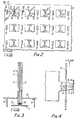
- Fig 1 The purpose of the embodiment of the invention illustrated in Fig 1 is to produce a beam which is narrow in azimuth as indicated at 1 on Figure 1 and to scan this in azimuth.
- the vertical shape of the beam is wider as shown in Figure 1.
- the antenna includes an array of dipoles 3 (Fig 2) arranged in vertical columns and horizontal rows. Each vertical column of dipoles is fed by a triplate 4 (Figs 1 and 3) having an inner conductor 5 (Fig 3) and outer conductors 6.
- Energy from a transmitter 7 is divided by a beam forming network 8 onto co-axial lines 9 with appropriate amplitude and phase adjustment to define the required beam shape in azimuth.
- the relative phases are electronically varied to provide horizontal scanning in azimuth.
- Each line 9 is connected by a socket 10 to one of the triplates 4.
- Each triplate forms a splitter designed to feed the energy to the individual dipoles 3 of a column with different relative phases and amplitudes to provide the specified vertical beam shape.
- the dipoles are not visible on Fig 1, being hidden by a ground plane 11 which is common to all the dipoles of all the triplates.
- Each vertical assembly of dipoles and its associated triplate is a discrete physical unit and these units are identical.
- Each dipole is built along similar principles to those described in our patent specification GB 2113476 and consists of a conductive plate 12 formed with an I shaped slot 13 ( Figure 2).
- each ground plane of the triplate is slotted at 14 to form arms 15.
- the top arm 15 of the ground plane visible in Figure 4 is connected to one side of the slot whilst the bottom arm 15 of the other ground plane is connected to the other side of the slot.
- a rod 16 connects the top arms together, and another rod 16 connects the bottom arms together.
- the rod connecting the top arms is also connected to the inner conductor 5.
- the distance between the dipoles 3 should ideally be one quarter of a wavelength at the centre frequency.
- the way in which the illustrated dipole operates is complex and is of no relevance to the present invention which is equally applicable to antenna formed from dipoles of conventional construction. It is sufficient to note that the effect of the illustrated design is to radiate energy in the manner of a conventional dipole having a vertical E plane and horizontal H plane as illustrated but which has a wide bandwidth and matches a standard 50 ohm feed.
- the parasitic projections are frequency sensitive and their lengths need to be accurately tuned empirically for a given frequency of operation to minimise mutual coupling.
- the tuned electrical length (which is longer than the physical .length) will in practice normally be less than a quarter of a wavelength, depending on the thickness and cross- sectional area of the projection. The thicker the projection the shorter it needs to be.
- the second embodiment of the invention is built along lines similar to those shown in Fig 1 but employs a different triplate structure as shown in Fig 5.
- the triplate of Fig 5 comprises two identical earthed conductive sheets 18 and 19 forming the earth planes of the triplate, one of these being removed in the case of Figure 5. Between the earth planes 18 and 19 are conductive strips 20 separated from the sheets 18 and 19 by insulating layers 21 and 22 of foam plastics material. Layers 18, 19, '21 and 22 are connected together by bolts, (one of which is shown at 23) arranged to establish electrical contact between the earth planes 18 and 19.
- Each dipole is formed by two members, each a quarter of a wavelength long, positioned on the end of an arm, which is also approximately a quarter of a wavelength long and extends from an edge (eg, edge 18A of one of the ground planes 18 or 19).
- the two members and the arm form a T shape.
- the said members of each T are separated by a slot 27 which extends from its open end to a closed end in the arm 28 of the T shape near where it joins the edge, e.g., 18A, of the ground plane 18 or 19.
- the conductive strips 20 forming the feeds terminate at each T shape in a U shaped portion which has a part 29 a quarter wavelength long extending along the arm 28 on one side of the slot 27; a part 30 extending across the slot immediately between the dipoles 28A and 28B formed by the members of the T; and a part 26 which is also a quarter wavelength long and extends back along the arm 28 on the opposite side of the slot to its free end which is just before the closed end of the slot 27.
- the U shaped portion of a feed strip 20 in co-operation with the arm of the associated T shape, split by the slot 27, forms a balun whose effect is to feed energy to the dipoles so that current always flows in the same direction in the two halves 28A, 28B of the dipole.
- each dipole 31 Between each dipole 31 is a post 32 (similar in function to posts 17) but formed by protrusions from the ground planes 18 and 19. The free ends of these protrusions 32 lie directly between the members 28A and 28B formed by the dipoles.
- the effect of the protrusions 27 is the same as that of the protrusions 17 (Figs 2 & 3), namely to prevent a substantial amount of mutual coupling between adjacent dipoles.
- triplate structures could be replaced by a stripline energy feeding systems or indeed by waveguides or co-axial cables.
- Another possibility would be to use two or more projections between each pair of dipoles. Where only one projection is used it is preferably positioned centrally between the dipoles but this is not essential and an offset configuration could also be used.
Abstract
Description
- This invention relates to an antenna comprising an array of dipoles arranged in rows and columns.
- A well known undesirable characteristic of such antennas is that strong coupling exists between adjacent dipoles. It is difficult to predict the nature of the coupling in any particular design and therefore to select the correct phase and amplitude values to be applied to each dipole in order to achieve a required beam shape. This problem is set out in a paper entitled "Mutual Coupling in Two-Dimensional Arrays" by J. Blass and S.J. Rabinowitz published by the Institute of Radio Engineers Western Convention Record Vol 1, Part 1 pages 134-150.
- This invention provides an antenna comprising an array of dipoles arranged in rows and columns in which a conductive projection is interposed between elements spaced in the E plane thereby reducing mutual coupling between the elements.
- By taking mutual coupling into consideration it is possible using conventional techniques to obtain a required beam shape but the effects of the mutual coupling are such that when it is desired to scan the beam the beam shape may be lost.
- The invention is therefore of particular value in antennas .adapted to produce a scanning beam and is considered to be of particular application to antenna structures of the type in which the dipoles are formed on the ends of arms extending from and distributed along one edge of a stripline or triplate structure for feeding energy to the dipoles. In such an arrangement conductive projections can conveniently be formed by protrusions from the said edge and preferably from a conductive layer or layers forming part of the stripline or triplate structure. The aforementioned arms and the dipoles can similarly be formed from further extensions of the same conductive layer or layers. In one arrangement the dipoles and the said arms form T shaped extensions of the ground planes of a triplate structure. Two ways in which the invention may be performed will now be described by way of example with reference to the accompanying drawings in which:-
- Figure 1 shows in very diagrammatic form an antenna constructed in accordance with the invention and seen from behind;
- Figure 2 is a front elevation of a part of the antenna of Figure 1 (showing twelve dipoles);
- Figure 3 is a horizontal cross-section through the line III - III on Figure 2,
- Figure 4 is a vertical cross section through the line IV-IV on Figure 2,.
- Figure 5 is a side view of one of a number of vertical triplate systems forming another antenna also constructed in accordance with the invention and shown with one of its earth planes and one of its dielectric sheets removed to reveal the central conductors; and
- Figure 6 is a cross-section through the line XX of Figure 5.
- The purpose of the embodiment of the invention illustrated in Fig 1 is to produce a beam which is narrow in azimuth as indicated at 1 on Figure 1 and to scan this in azimuth. The vertical shape of the beam is wider as shown in Figure 1.
- The antenna includes an array of dipoles 3 (Fig 2) arranged in vertical columns and horizontal rows. Each vertical column of dipoles is fed by a triplate 4 (Figs 1 and 3) having an inner conductor 5 (Fig 3) and
outer conductors 6. - Energy from a transmitter 7 is divided by a
beam forming network 8 ontoco-axial lines 9 with appropriate amplitude and phase adjustment to define the required beam shape in azimuth. The relative phases are electronically varied to provide horizontal scanning in azimuth. Eachline 9 is connected by asocket 10 to one of thetriplates 4. Each triplate forms a splitter designed to feed the energy to theindividual dipoles 3 of a column with different relative phases and amplitudes to provide the specified vertical beam shape. The dipoles are not visible on Fig 1, being hidden by aground plane 11 which is common to all the dipoles of all the triplates. - Each vertical assembly of dipoles and its associated triplate is a discrete physical unit and these units are identical.
- Each dipole is built along similar principles to those described in our patent specification GB 2113476 and consists of a
conductive plate 12 formed with an I shaped slot 13 (Figure 2). Referring to Figure 4 each ground plane of the triplate is slotted at 14 to formarms 15. Thetop arm 15 of the ground plane visible in Figure 4 is connected to one side of the slot whilst thebottom arm 15 of the other ground plane is connected to the other side of the slot. Arod 16 connects the top arms together, and anotherrod 16 connects the bottom arms together. The rod connecting the top arms is also connected to theinner conductor 5. Aconductive sheet 11, which is common to all the dipoles, forms a ground reflector which provides a unidirectional radiation pattern. The distance between thedipoles 3 should ideally be one quarter of a wavelength at the centre frequency. The way in which the illustrated dipole operates is complex and is of no relevance to the present invention which is equally applicable to antenna formed from dipoles of conventional construction. It is sufficient to note that the effect of the illustrated design is to radiate energy in the manner of a conventional dipole having a vertical E plane and horizontal H plane as illustrated but which has a wide bandwidth and matches a standard 50 ohm feed. - In a system as described so far there is a problem as follows. Due to strong horizontal coupling between dipole elements of a vertical column, the required elevation beam shape of Figure 1 is lost during horizontal scanning. This problem is one which is well known in the art and to which no entirely satisfactory solution has previously been found. In the illustrated embodiment the problem is overcome to a satisfactory extent by the introduction of parasitic
conductive projections 17 in between dipoles in the E plane. The action of aparasitic projection 17 is to absorb some of the power from a dipole and to re-radiate it at a low angle to theground plane 11 to provide for a broader beam from individual dipoles as is required for a broad beam scanning. At the same time the parasitic element prevents the power being radiated from one element to the adjacent element or elements in the E plane. - The parasitic projections are frequency sensitive and their lengths need to be accurately tuned empirically for a given frequency of operation to minimise mutual coupling. The tuned electrical length (which is longer than the physical .length) will in practice normally be less than a quarter of a wavelength, depending on the thickness and cross- sectional area of the projection. The thicker the projection the shorter it needs to be.
- The second embodiment of the invention is built along lines similar to those shown in Fig 1 but employs a different triplate structure as shown in Fig 5. The triplate of Fig 5 comprises two identical earthed
conductive sheets earth planes conductive strips 20 separated from thesheets layers Layers earth planes - Energy to be transmitted is fed from a co-axial line (not shown but similar to that shown at 9 on Fig 1) to a
co-axial socket 24 shown in more detail in Figure 6. - From the
co-axial socket 24 energy is transmitted to a centreconductive strip 20 of the triplate, anelement 25 being included to improve coupling from the co-axial socket to the triplate. From the centreconductive strip 20 the energy is transmitted along circuitous paths to each of an array ofdipole elements 31. The routes to the dipoles are arranged to feed energy so that it arrives at the dipoles with a desired phase and amplitude distribution. - Each dipole is formed by two members, each a quarter of a wavelength long, positioned on the end of an arm, which is also approximately a quarter of a wavelength long and extends from an edge (eg,
edge 18A of one of theground planes 18 or 19). The two members and the arm form a T shape. The said members of each T are separated by aslot 27 which extends from its open end to a closed end in thearm 28 of the T shape near where it joins the edge, e.g., 18A, of theground plane - The
conductive strips 20 forming the feeds, terminate at each T shape in a U shaped portion which has a part 29 a quarter wavelength long extending along thearm 28 on one side of theslot 27; apart 30 extending across the slot immediately between thedipoles part 26 which is also a quarter wavelength long and extends back along thearm 28 on the opposite side of the slot to its free end which is just before the closed end of theslot 27. The U shaped portion of afeed strip 20 in co-operation with the arm of the associated T shape, split by theslot 27, forms a balun whose effect is to feed energy to the dipoles so that current always flows in the same direction in the twohalves - Between each
dipole 31 is a post 32 (similar in function to posts 17) but formed by protrusions from theground planes protrusions 32 lie directly between themembers protrusions 27 is the same as that of the protrusions 17 (Figs 2 & 3), namely to prevent a substantial amount of mutual coupling between adjacent dipoles. - It will be appreciated that the illustrated embodiments have been described only as an example of two ways in which the invention can be performed. In another configuration the triplate structures could be replaced by a stripline energy feeding systems or indeed by waveguides or co-axial cables. Another possibility would be to use two or more projections between each pair of dipoles. Where only one projection is used it is preferably positioned centrally between the dipoles but this is not essential and an offset configuration could also be used.
Claims (3)
Applications Claiming Priority (4)
| Application Number | Priority Date | Filing Date | Title |
|---|---|---|---|
| GB08432186A GB2171257A (en) | 1984-12-20 | 1984-12-20 | A dipole array |
| GB8432186 | 1984-12-20 | ||
| GB8523076 | 1985-09-18 | ||
| GB858523076A GB8523076D0 (en) | 1984-12-20 | 1985-09-18 | Dipole array |
Publications (2)
| Publication Number | Publication Date |
|---|---|
| EP0186455A2 true EP0186455A2 (en) | 1986-07-02 |
| EP0186455A3 EP0186455A3 (en) | 1987-11-25 |
Family
ID=26288598
Family Applications (1)
| Application Number | Title | Priority Date | Filing Date |
|---|---|---|---|
| EP85309297A Withdrawn EP0186455A3 (en) | 1984-12-20 | 1985-12-19 | A dipole array |
Country Status (4)
| Country | Link |
|---|---|
| US (1) | US5039994A (en) |
| EP (1) | EP0186455A3 (en) |
| ES (1) | ES8801066A1 (en) |
| GB (1) | GB2170357B (en) |
Cited By (12)
| Publication number | Priority date | Publication date | Assignee | Title |
|---|---|---|---|---|
| EP0249303A1 (en) * | 1986-05-28 | 1987-12-16 | THE GENERAL ELECTRIC COMPANY, p.l.c. | A dipole array |
| EP0409222A2 (en) * | 1989-07-21 | 1991-01-23 | SELENIA INDUSTRIE ELETTRONICHE ASSOCIATE S.p.A. | RF partitioning network for array antenna |
| EP0409221A2 (en) * | 1989-07-21 | 1991-01-23 | SELENIA INDUSTRIE ELETTRONICHE ASSOCIATE S.p.A. | Integrated structure with radiating elements and dividing networks for application to radar antenna |
| FR2685822A1 (en) * | 1991-12-31 | 1993-07-02 | Thomson Csf | PHASE CONTROL REFLECTIVE ARRAY. |
| EP0559980A1 (en) * | 1992-03-11 | 1993-09-15 | Siemens Plessey Electronic Systems Limited | Antenna choke |
| EP0573971A1 (en) * | 1992-06-11 | 1993-12-15 | Rohde & Schwarz GmbH & Co. KG | Antenna |
| EP0624918A1 (en) * | 1993-05-14 | 1994-11-17 | Gec-Marconi Electronic Systems Corporation | Full aperture interleaved space duplexed beamshaped microstrip antenna system |
| EP0666610A1 (en) * | 1994-02-07 | 1995-08-09 | Motorola, Inc. | Substrate integrated antenna |
| EP0700115A1 (en) * | 1994-09-02 | 1996-03-06 | Hollandse Signaalapparaten B.V. | Stripline antenna |
| EP0730319A1 (en) * | 1995-03-03 | 1996-09-04 | Ace Antenna Corporation | An antenna system having a choke reflector for minimizing sideward radiation |
| EP2045875A1 (en) | 2007-10-02 | 2009-04-08 | The Furukawa Electric Co., Ltd. | Antenna for radar device |
| EP2211423A3 (en) * | 2009-01-26 | 2010-08-04 | The Furukawa Electric Co., Ltd. | Radar antenna |
Families Citing this family (38)
| Publication number | Priority date | Publication date | Assignee | Title |
|---|---|---|---|---|
| CA2011298C (en) * | 1990-03-01 | 1999-05-25 | Adrian William Alden | Dual polarization dipole array antenna |
| US5191349A (en) * | 1990-08-08 | 1993-03-02 | Honeywell Inc. | Apparatus and method for an amplitude monopulse directional antenna |
| US5309164A (en) * | 1992-04-13 | 1994-05-03 | Andrew Corporation | Patch-type microwave antenna having wide bandwidth and low cross-pol |
| DE4218544A1 (en) * | 1992-06-05 | 1993-12-16 | Abb Patent Gmbh | Shortwave transmitter antenna |
| US5943017A (en) * | 1995-12-13 | 1999-08-24 | Ail Systems, Inc. | Dual near-field focused antenna array |
| US5673052A (en) * | 1995-12-13 | 1997-09-30 | Dorne & Margolin, Inc. | Near-field focused antenna |
| GB2312791A (en) * | 1996-05-02 | 1997-11-05 | Northern Telecom Ltd | Antenna array assembly |
| US5940048A (en) | 1996-07-16 | 1999-08-17 | Metawave Communications Corporation | Conical omni-directional coverage multibeam antenna |
| US5872547A (en) * | 1996-07-16 | 1999-02-16 | Metawave Communications Corporation | Conical omni-directional coverage multibeam antenna with parasitic elements |
| US5892486A (en) * | 1996-10-11 | 1999-04-06 | Channel Master Llc | Broad band dipole element and array |
| US6084530A (en) * | 1996-12-30 | 2000-07-04 | Lucent Technologies Inc. | Modulated backscatter sensor system |
| US6130623A (en) * | 1996-12-31 | 2000-10-10 | Lucent Technologies Inc. | Encryption for modulated backscatter systems |
| US6046683A (en) * | 1996-12-31 | 2000-04-04 | Lucent Technologies Inc. | Modulated backscatter location system |
| US6184841B1 (en) * | 1996-12-31 | 2001-02-06 | Lucent Technologies Inc. | Antenna array in an RFID system |
| US6456668B1 (en) | 1996-12-31 | 2002-09-24 | Lucent Technologies Inc. | QPSK modulated backscatter system |
| FR2766626B1 (en) * | 1997-07-28 | 1999-10-01 | Alsthom Cge Alcatel | CROSS POLARIZATION DIRECTIONAL ANTENNA SYSTEM |
| US6097931A (en) * | 1997-08-20 | 2000-08-01 | Wireless Online, Inc. | Two-way paging uplink infrastructure |
| FI990395A (en) | 1999-02-24 | 2000-08-25 | Nokia Networks Oy | Hardware for attenuating interference between antennas |
| US6369710B1 (en) | 2000-03-27 | 2002-04-09 | Lucent Technologies Inc. | Wireless security system |
| US6387191B1 (en) * | 2000-07-21 | 2002-05-14 | Transportation Technology Center, Inc. | Railway wheels resistant to martensite transformation |
| AU2001290379A1 (en) * | 2000-09-12 | 2002-03-26 | Andrew Corporation | A dual polarised antenna |
| US6795035B2 (en) * | 2002-03-28 | 2004-09-21 | Lucent Technologies Inc. | System for antenna sidelobe modification |
| US7529525B1 (en) * | 2002-04-16 | 2009-05-05 | Faulkner Interstices Llc | Method and apparatus for collecting information for use in a smart antenna system |
| US7289826B1 (en) * | 2002-04-16 | 2007-10-30 | Faulkner Interstices, Llc | Method and apparatus for beam selection in a smart antenna system |
| US7346365B1 (en) * | 2002-04-16 | 2008-03-18 | Faulkner Interstices Llc | Smart antenna system and method |
| US7065383B1 (en) * | 2002-04-16 | 2006-06-20 | Omri Hovers | Method and apparatus for synchronizing a smart antenna apparatus with a base station transceiver |
| US20050219140A1 (en) * | 2004-04-01 | 2005-10-06 | Stella Doradus Waterford Limited | Antenna construction |
| US7525502B2 (en) * | 2004-08-20 | 2009-04-28 | Nokia Corporation | Isolation between antennas using floating parasitic elements |
| US7557675B2 (en) * | 2005-03-22 | 2009-07-07 | Radiacion Y Microondas, S.A. | Broad band mechanical phase shifter |
| KR100859864B1 (en) * | 2005-06-13 | 2008-09-24 | 삼성전자주식회사 | Plate board type MIMO array antenna comprising isolation element |
| US7385560B1 (en) * | 2006-09-26 | 2008-06-10 | Rockwell Collins, Inc. | Aircraft directional/omnidirectional antenna arrangement |
| JP5068061B2 (en) * | 2006-10-30 | 2012-11-07 | パナソニック株式会社 | Antenna device |
| WO2009052153A1 (en) * | 2007-10-15 | 2009-04-23 | Jaybeam Wireless | Base station antenna with beam shaping structures |
| KR20140136516A (en) | 2012-03-26 | 2014-11-28 | 갈트로닉스 코포레이션 리미티드 | Isolation structures for dual-polarized antennas |
| EP3100518B1 (en) * | 2014-01-31 | 2020-12-23 | Quintel Cayman Limited | Antenna system with beamwidth control |
| US11145968B2 (en) | 2017-03-29 | 2021-10-12 | Nihon Dengyo Kosaku Co., Ltd. | Array antenna and sector antenna |
| US10680332B1 (en) | 2018-12-28 | 2020-06-09 | Industrial Technology Research Institute | Hybrid multi-band antenna array |
| KR102608773B1 (en) * | 2019-02-14 | 2023-12-04 | 삼성전자주식회사 | Antenna module and electronic device including the same |
Citations (7)
| Publication number | Priority date | Publication date | Assignee | Title |
|---|---|---|---|---|
| US2455403A (en) * | 1945-01-20 | 1948-12-07 | Rca Corp | Antenna |
| US3750185A (en) * | 1972-01-18 | 1973-07-31 | Westinghouse Electric Corp | Dipole antenna array |
| GB1398262A (en) * | 1971-08-05 | 1975-06-18 | Emi Ltd | Aerials |
| US3958247A (en) * | 1974-12-23 | 1976-05-18 | Rca Corporation | Rf power coupling network employing a parallel plate transmission line |
| FR2390027A1 (en) * | 1977-05-05 | 1978-12-01 | Thomson Csf | Attenuation of slotted waveguide aerial parasitic side lobes - is achieved by plate filter installed in plane of emission |
| US4131896A (en) * | 1976-02-10 | 1978-12-26 | Westinghouse Electric Corp. | Dipole phased array with capacitance plate elements to compensate for impedance variations over the scan angle |
| EP0056985A2 (en) * | 1981-01-24 | 1982-08-04 | Metalltechnik Schmidt GmbH & Co. | Device to improve the decoupling of antennae |
Family Cites Families (10)
| Publication number | Priority date | Publication date | Assignee | Title |
|---|---|---|---|---|
| US2130033A (en) * | 1934-07-05 | 1938-09-13 | Telefunken Gmbh | Directive beam radiator |
| US2573914A (en) * | 1949-07-30 | 1951-11-06 | Rca Corp | Antenna system |
| US2691102A (en) * | 1950-08-14 | 1954-10-05 | Rca Corp | High gain vhf antenna system |
| US3541559A (en) * | 1968-04-10 | 1970-11-17 | Westinghouse Electric Corp | Antenna for producing circular polarization over wide angles |
| US3545001A (en) * | 1968-04-24 | 1970-12-01 | Bendix Corp | Antenna feed comprising dipole array with conductive ground plane |
| US3681770A (en) * | 1970-01-14 | 1972-08-01 | Andrew Alford | Isolating antenna elements |
| US3887925A (en) * | 1973-07-31 | 1975-06-03 | Itt | Linearly polarized phased antenna array |
| FR2490026A1 (en) * | 1980-09-09 | 1982-03-12 | Thomson Csf | NON-DISPERSIVE NETWORK ANTENNA AND ITS APPLICATION TO THE PRODUCTION OF AN ELECTRONIC SCANNING ANTENNA |
| DE3224545A1 (en) * | 1982-07-01 | 1984-01-05 | Licentia Patent-Verwaltungs-Gmbh, 6000 Frankfurt | GROUP ANTENNA |
| GB2135829B (en) * | 1983-02-24 | 1986-04-09 | Cossor Electronics Ltd | An antenna with a reflector of open construction |
-
1985
- 1985-12-19 GB GB08531269A patent/GB2170357B/en not_active Expired
- 1985-12-19 EP EP85309297A patent/EP0186455A3/en not_active Withdrawn
- 1985-12-19 ES ES550170A patent/ES8801066A1/en not_active Expired
-
1989
- 1989-11-13 US US07/434,461 patent/US5039994A/en not_active Expired - Fee Related
Patent Citations (7)
| Publication number | Priority date | Publication date | Assignee | Title |
|---|---|---|---|---|
| US2455403A (en) * | 1945-01-20 | 1948-12-07 | Rca Corp | Antenna |
| GB1398262A (en) * | 1971-08-05 | 1975-06-18 | Emi Ltd | Aerials |
| US3750185A (en) * | 1972-01-18 | 1973-07-31 | Westinghouse Electric Corp | Dipole antenna array |
| US3958247A (en) * | 1974-12-23 | 1976-05-18 | Rca Corporation | Rf power coupling network employing a parallel plate transmission line |
| US4131896A (en) * | 1976-02-10 | 1978-12-26 | Westinghouse Electric Corp. | Dipole phased array with capacitance plate elements to compensate for impedance variations over the scan angle |
| FR2390027A1 (en) * | 1977-05-05 | 1978-12-01 | Thomson Csf | Attenuation of slotted waveguide aerial parasitic side lobes - is achieved by plate filter installed in plane of emission |
| EP0056985A2 (en) * | 1981-01-24 | 1982-08-04 | Metalltechnik Schmidt GmbH & Co. | Device to improve the decoupling of antennae |
Cited By (17)
| Publication number | Priority date | Publication date | Assignee | Title |
|---|---|---|---|---|
| EP0249303A1 (en) * | 1986-05-28 | 1987-12-16 | THE GENERAL ELECTRIC COMPANY, p.l.c. | A dipole array |
| EP0409222A2 (en) * | 1989-07-21 | 1991-01-23 | SELENIA INDUSTRIE ELETTRONICHE ASSOCIATE S.p.A. | RF partitioning network for array antenna |
| EP0409221A2 (en) * | 1989-07-21 | 1991-01-23 | SELENIA INDUSTRIE ELETTRONICHE ASSOCIATE S.p.A. | Integrated structure with radiating elements and dividing networks for application to radar antenna |
| EP0409221A3 (en) * | 1989-07-21 | 1991-10-30 | Selenia Industrie Elettroniche Associate S.P.A. | Integrated structure with radiating elements and dividing networks for application to radar antenna |
| EP0409222A3 (en) * | 1989-07-21 | 1992-01-08 | Selenia Industrie Elettroniche Associate S.P.A. | Rf partitioning network for array antenna |
| FR2685822A1 (en) * | 1991-12-31 | 1993-07-02 | Thomson Csf | PHASE CONTROL REFLECTIVE ARRAY. |
| EP0551780A1 (en) * | 1991-12-31 | 1993-07-21 | Thomson-Csf | A phase controlled reflector antenna array |
| EP0559980A1 (en) * | 1992-03-11 | 1993-09-15 | Siemens Plessey Electronic Systems Limited | Antenna choke |
| EP0573971A1 (en) * | 1992-06-11 | 1993-12-15 | Rohde & Schwarz GmbH & Co. KG | Antenna |
| EP0624918A1 (en) * | 1993-05-14 | 1994-11-17 | Gec-Marconi Electronic Systems Corporation | Full aperture interleaved space duplexed beamshaped microstrip antenna system |
| EP0666610A1 (en) * | 1994-02-07 | 1995-08-09 | Motorola, Inc. | Substrate integrated antenna |
| EP0700115A1 (en) * | 1994-09-02 | 1996-03-06 | Hollandse Signaalapparaten B.V. | Stripline antenna |
| NL9401429A (en) * | 1994-09-02 | 1996-04-01 | Hollandse Signaalapparaten Bv | Stripline antenna. |
| US5917456A (en) * | 1994-09-02 | 1999-06-29 | Hollandse Signaalapparaten B.V. | Stripline antenna |
| EP0730319A1 (en) * | 1995-03-03 | 1996-09-04 | Ace Antenna Corporation | An antenna system having a choke reflector for minimizing sideward radiation |
| EP2045875A1 (en) | 2007-10-02 | 2009-04-08 | The Furukawa Electric Co., Ltd. | Antenna for radar device |
| EP2211423A3 (en) * | 2009-01-26 | 2010-08-04 | The Furukawa Electric Co., Ltd. | Radar antenna |
Also Published As
| Publication number | Publication date |
|---|---|
| ES8801066A1 (en) | 1987-12-01 |
| GB2170357A (en) | 1986-07-30 |
| GB8531269D0 (en) | 1986-01-29 |
| ES550170A0 (en) | 1987-12-01 |
| US5039994A (en) | 1991-08-13 |
| GB2170357B (en) | 1988-07-13 |
| EP0186455A3 (en) | 1987-11-25 |
Similar Documents
| Publication | Publication Date | Title |
|---|---|---|
| EP0186455A2 (en) | A dipole array | |
| US3836976A (en) | Closely spaced orthogonal dipole array | |
| US4684952A (en) | Microstrip reflectarray for satellite communication and radar cross-section enhancement or reduction | |
| JPS581846B2 (en) | Antenna array with radiating slot opening | |
| US4398199A (en) | Circularly polarized microstrip line antenna | |
| US4203118A (en) | Antenna for cross polarized waves | |
| JP3943140B2 (en) | Equipment in antenna units | |
| US6130648A (en) | Double slot array antenna | |
| GB2220303A (en) | Dual polarised phased array antenna | |
| US4918457A (en) | Antenna formed of strip transmission lines with non-conductive coupling | |
| EP0345454B1 (en) | Microstrip array antenna | |
| US4575728A (en) | Dipole array with means for compensating feedline parasitic currents | |
| US5633646A (en) | Mini-cap radiating element | |
| US4912482A (en) | Antenna | |
| US2794185A (en) | Antenna systems | |
| US3757343A (en) | Slot antenna array | |
| US5614915A (en) | Layered antenna | |
| US5559523A (en) | Layered antenna | |
| EP0542447B1 (en) | Flat plate antenna | |
| US4516132A (en) | Antenna with a reflector of open construction | |
| US4250509A (en) | Circularly polarized zigzag antenna | |
| GB2171257A (en) | A dipole array | |
| US6046704A (en) | Stamp-and-bend double-tuned radiating elements and antennas | |
| US3299430A (en) | Parallel dipole array supported on insulator having a low dielectric constant | |
| US3740751A (en) | Wideband dual-slot waveguide array |
Legal Events
| Date | Code | Title | Description |
|---|---|---|---|
| PUAI | Public reference made under article 153(3) epc to a published international application that has entered the european phase |
Free format text: ORIGINAL CODE: 0009012 |
|
| AK | Designated contracting states |
Kind code of ref document: A2 Designated state(s): DE FR IT NL SE |
|
| PUAL | Search report despatched |
Free format text: ORIGINAL CODE: 0009013 |
|
| AK | Designated contracting states |
Kind code of ref document: A3 Designated state(s): DE FR IT NL SE |
|
| 17P | Request for examination filed |
Effective date: 19871209 |
|
| 17Q | First examination report despatched |
Effective date: 19890321 |
|
| STAA | Information on the status of an ep patent application or granted ep patent |
Free format text: STATUS: THE APPLICATION IS DEEMED TO BE WITHDRAWN |
|
| 18D | Application deemed to be withdrawn |
Effective date: 19920114 |
|
| RIN1 | Information on inventor provided before grant (corrected) |
Inventor name: WOLOSZCZUK, EDMUND WERGILIUSZ Inventor name: WASH, RICHARD GARWOOD |