EP0186540A1 - Electronic circuit composed of thin-film transistors for controlling a matrix device - Google Patents
Electronic circuit composed of thin-film transistors for controlling a matrix device Download PDFInfo
- Publication number
- EP0186540A1 EP0186540A1 EP85402238A EP85402238A EP0186540A1 EP 0186540 A1 EP0186540 A1 EP 0186540A1 EP 85402238 A EP85402238 A EP 85402238A EP 85402238 A EP85402238 A EP 85402238A EP 0186540 A1 EP0186540 A1 EP 0186540A1
- Authority
- EP
- European Patent Office
- Prior art keywords
- film transistors
- register
- transistors
- matrix
- group
- Prior art date
- Legal status (The legal status is an assumption and is not a legal conclusion. Google has not performed a legal analysis and makes no representation as to the accuracy of the status listed.)
- Granted
Links
- 239000011159 matrix material Substances 0.000 title claims abstract description 50
- 239000010409 thin film Substances 0.000 title claims abstract description 33
- 239000003990 capacitor Substances 0.000 description 10
- 238000004519 manufacturing process Methods 0.000 description 6
- 229910021417 amorphous silicon Inorganic materials 0.000 description 5
- 239000011521 glass Substances 0.000 description 4
- 239000004973 liquid crystal related substance Substances 0.000 description 4
- 230000002093 peripheral effect Effects 0.000 description 4
- 210000001525 retina Anatomy 0.000 description 4
- VYPSYNLAJGMNEJ-UHFFFAOYSA-N Silicium dioxide Chemical compound O=[Si]=O VYPSYNLAJGMNEJ-UHFFFAOYSA-N 0.000 description 2
- 229910052782 aluminium Inorganic materials 0.000 description 2
- XAGFODPZIPBFFR-UHFFFAOYSA-N aluminium Chemical compound [Al] XAGFODPZIPBFFR-UHFFFAOYSA-N 0.000 description 2
- 210000004027 cell Anatomy 0.000 description 2
- 238000000151 deposition Methods 0.000 description 2
- 230000006870 function Effects 0.000 description 2
- 238000000034 method Methods 0.000 description 2
- 229910052814 silicon oxide Inorganic materials 0.000 description 2
- ATJFFYVFTNAWJD-UHFFFAOYSA-N Tin Chemical compound [Sn] ATJFFYVFTNAWJD-UHFFFAOYSA-N 0.000 description 1
- 239000013078 crystal Substances 0.000 description 1
- 210000002858 crystal cell Anatomy 0.000 description 1
- 230000007547 defect Effects 0.000 description 1
- 230000001419 dependent effect Effects 0.000 description 1
- 230000008021 deposition Effects 0.000 description 1
- 235000021183 entrée Nutrition 0.000 description 1
- 210000003128 head Anatomy 0.000 description 1
- 229910003437 indium oxide Inorganic materials 0.000 description 1
- PJXISJQVUVHSOJ-UHFFFAOYSA-N indium(iii) oxide Chemical compound [O-2].[O-2].[O-2].[In+3].[In+3] PJXISJQVUVHSOJ-UHFFFAOYSA-N 0.000 description 1
- 239000007788 liquid Substances 0.000 description 1
- 230000003287 optical effect Effects 0.000 description 1
- 238000002161 passivation Methods 0.000 description 1
- 238000009877 rendering Methods 0.000 description 1
- HBMJWWWQQXIZIP-UHFFFAOYSA-N silicon carbide Chemical compound [Si+]#[C-] HBMJWWWQQXIZIP-UHFFFAOYSA-N 0.000 description 1
- 229910001887 tin oxide Inorganic materials 0.000 description 1
Images
Classifications
-
- G—PHYSICS
- G09—EDUCATION; CRYPTOGRAPHY; DISPLAY; ADVERTISING; SEALS
- G09G—ARRANGEMENTS OR CIRCUITS FOR CONTROL OF INDICATING DEVICES USING STATIC MEANS TO PRESENT VARIABLE INFORMATION
- G09G3/00—Control arrangements or circuits, of interest only in connection with visual indicators other than cathode-ray tubes
- G09G3/20—Control arrangements or circuits, of interest only in connection with visual indicators other than cathode-ray tubes for presentation of an assembly of a number of characters, e.g. a page, by composing the assembly by combination of individual elements arranged in a matrix no fixed position being assigned to or needed to be assigned to the individual characters or partial characters
- G09G3/34—Control arrangements or circuits, of interest only in connection with visual indicators other than cathode-ray tubes for presentation of an assembly of a number of characters, e.g. a page, by composing the assembly by combination of individual elements arranged in a matrix no fixed position being assigned to or needed to be assigned to the individual characters or partial characters by control of light from an independent source
- G09G3/36—Control arrangements or circuits, of interest only in connection with visual indicators other than cathode-ray tubes for presentation of an assembly of a number of characters, e.g. a page, by composing the assembly by combination of individual elements arranged in a matrix no fixed position being assigned to or needed to be assigned to the individual characters or partial characters by control of light from an independent source using liquid crystals
- G09G3/3611—Control of matrices with row and column drivers
- G09G3/3685—Details of drivers for data electrodes
- G09G3/3688—Details of drivers for data electrodes suitable for active matrices only
-
- G—PHYSICS
- G09—EDUCATION; CRYPTOGRAPHY; DISPLAY; ADVERTISING; SEALS
- G09G—ARRANGEMENTS OR CIRCUITS FOR CONTROL OF INDICATING DEVICES USING STATIC MEANS TO PRESENT VARIABLE INFORMATION
- G09G3/00—Control arrangements or circuits, of interest only in connection with visual indicators other than cathode-ray tubes
- G09G3/20—Control arrangements or circuits, of interest only in connection with visual indicators other than cathode-ray tubes for presentation of an assembly of a number of characters, e.g. a page, by composing the assembly by combination of individual elements arranged in a matrix no fixed position being assigned to or needed to be assigned to the individual characters or partial characters
-
- G—PHYSICS
- G09—EDUCATION; CRYPTOGRAPHY; DISPLAY; ADVERTISING; SEALS
- G09G—ARRANGEMENTS OR CIRCUITS FOR CONTROL OF INDICATING DEVICES USING STATIC MEANS TO PRESENT VARIABLE INFORMATION
- G09G2310/00—Command of the display device
- G09G2310/02—Addressing, scanning or driving the display screen or processing steps related thereto
- G09G2310/0264—Details of driving circuits
- G09G2310/0297—Special arrangements with multiplexing or demultiplexing of display data in the drivers for data electrodes, in a pre-processing circuitry delivering display data to said drivers or in the matrix panel, e.g. multiplexing plural data signals to one D/A converter or demultiplexing the D/A converter output to multiple columns
Definitions
- the present invention relates to an electronic circuit formed of thin film transistors used to control a matrix device.
- the invention relates to an electronic circuit of the shift register type used to sequentially control the rows or columns of a matrix device and in particular the rows or columns of a crystal display device liquids (flat screen with active matrix, screen for dashboard, ...), photosensitive video retinas with thin film transistors, optical sensors or rendering heads for fax systems with photodiodes lines, sensors, etc ...
- an electronic memory formed by memory points distributed over the entire surface of the screen stores the video signal throughout the duration of the image.
- An electro-optical transducer in particular a liquid crystal transducer, is in contact with each memory point and is excited throughout the duration of the image.
- Each memory point is located at the intersection of a line and a connection column and it consists of a thin-film transistor produced on an insulating support and a capacitor of which the armatures are made, in the case where the transducer is a liquid crystal, by the electrodes of the liquid crystal cell itself, the insulating support constituting one of the two walls of said cell.
- Each stage of the shift register generally comprises two elementary inverters and a capacitor used to store the video information.
- each inverter is formed of at least two thin film transistors, arranged in cascade.
- the thin film transistors of the active matrix are generally produced with amorphous silicon, these have a low transconductance and a high input capacity, which leads to obtaining a limit frequency of relatively low inverter operation and most of the time lower than the scanning frequency of the lines of a high complexity flat screen (300 to 500 lines).
- shift registers of the charge transfer type such as the Bucket-Brigade-Device (BBD) or the Coupled-Charge-Device (CCD) in Anglo-Saxon terminology, less greedy in number of TCM, but the density of defects in amorphous silicon has led to ineffective charge transfer.
- BBD Bucket-Brigade-Device
- CCD Coupled-Charge-Device
- the cost price of these screens is high due to the cost of the control circuits and the number of connections to be made between the flat screens and the corresponding circuits, or the number of welds to be made on the glass holder. It is generally accepted that the set of peripheral integrated circuits, that is to say the set of control circuits for the lines and the control circuits for the columns of the flat screen, represents half and even more than the price of total returns from said screen.
- the subject of the present invention is precisely an electronic circuit formed of thin film transistors used to control matrix devices and in particular flat screens with active matrix making it possible to remedy the various drawbacks mentioned above.
- peripheral integrated circuits With the active matrix while minimizing the cost of these circuits and therefore the overall price of flat screens by reducing the number of these peripheral circuits.
- the invention relates to an electronic circuit, used to control the rows or columns of a matrix device, using pa ⁇ t standard integrated circuits external to the device to provide the shift register function and d on the other hand, thin film transistors to provide the multiplexing function.
- the invention relates to an electronic control circuit with Nxn outputs used to control Nxn rows or columns of a matrix device, and in particular of a matrix display device, characterized in that it comprises a multiplexing circuit, formed by N groups of n successive thin-film transistors, a first shift register with N outputs and a second shift register with n outputs, the gates of the n transistors of the same group being connected to the same output of the first register, each group corresponding to a different output of said first register, the source of each transistor being connected to a different row or column, the drain of the i-th transistor of each group being connected to the i-th output of the second register, i being an integer such as 1 5 i n.
- matrix device can be understood a device comprising only one row or one column of components.
- These electronic control circuits only comprise two external integrated circuits, which are the two shift registers, making it possible to supply, via the multiplexing circuit, Nxn lines or columns of a matrix device and in particular of a screen. active matrix dish. This therefore makes it possible to reduce the number of connections to be made between the external circuits and the flat screen as well as to reduce the cost price of these flat screens.
- the transistors in thin layers of the multiplexing circuit of the control circuit of the invention can advantageously be produced on said support and simultaneously with the transistors of the matrix device.
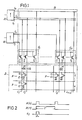
- an electronic control circuit has been shown in accordance with the invention making it possible to control Nxn lines of a flat screen with active matrix, bearing the general reference 2.
- This active matrix 2 is formed, in a conventional manner, of several conductive columns 4 and Nxn conductive lines denoted L j , j being an integer ranging from 1 to Nxn.
- L j Nxn conductive lines
- This active matrix 2 further comprises Nxn capacitors 14, one of the plates of each capacitor being connected to ground, the other to one of the conductive lines L j of the matrix 2.
- control circuit of NxN conductive lines L j of the matrix 2 is formed, on the one hand to a multiplexing circuit, of general reference 1 6, consisting of N groups G ,, ..., G N thin-film transistors, each group G i comprising n successive transistors T 1 , ... T n , and on the other hand a first shift register 18, comprising N outputs, and a second shift register 20 with n outputs.
- Such a control circuit makes it possible to considerably reduce the number of connections to be made between the control circuit and the active matrix, these connections being reduced to N + n connections instead of Nxn connections for the matrix devices of the prior art.
- each conductive line L j of the active matrix 2 is supplied by the source of a single thin film transistor; for example the source of the first transistor T, of group G, is connected to line L 1 , the source of the second transistor T 2 of group G, is connected to line L, and so on and the source of the last transistor T n of group G N at line L N. n .
- the gates of the N consecutive transistors T 1 , ... T n of the same group G; are connected to the same output P; from the first shift register 18, to each group corresponding to a different output P i from said first register.
- the gates of the transistors T 1 , ... T n of the group G, of transistors are all connected to the output P, of the first register 18, and the gates of the transistors T 1 , ... T n of the group G N of transistors are all connected to the output P N of said first register 18.
- the drains of the Nxn thin film transistors they are supplied so that the drain of the i th transistor T i of each group Ci is connected to the i th output Si of the second register 20, i being an integer such that 1 ⁇ i ⁇ not.
- the first transistors denoted T, of each group of transistors G 1 , ... G N are all connected to the first output S, of the second shift register 20, the second transistors T, of groups of transistors G 1 , ... G N are all connected to the output S2 of the second register 20, ... and the last transistors T of the groups G 1 , ... G N of transistors are all connected to the last output S n of the second register 20 .
- the signal R (n) corresponds to the output signal of the shift register 20
- the signal R (N) corresponds to the output signal of the shift register 18
- the signal L corresponds to the input signal of the first conductive line of the matrix 2.
- Each pulse of duration r, delivered by the register 20, corresponds to the access time to a conductive line of the matrix, r being close to 64 ⁇ s and the pulse r ', delivered by the register 18, is equal to nx ⁇ .
- a voltage pulse r, delivered by the shift register 18 which operates at the scanning frequency of the lines of the flat screen, will only be transmitted to a line of said screen in the group G i made passing by the pulse ⁇ ' , provided by the shift register 18.
- the corresponding lines of the flat screen are kept low thanks to the line capacitor 14 which remains charged throughout the duration of an image on the 'screen.
- the transistors 10 of the active matrix 2 are thin film transistors produced on an insulating support such as glass, constituting in particular one of the two walls of the flat screen between which is disposed the liquid crystal
- the thin film transistors of the multiplexing circuit 16 may advantageously be produced on said support and simultaneously with the manufacture of the transistors 10 of the active matrix 2 of the screen.
- the two shift registers 18 and 20 will be standard integrated circuits, produced independently of the active matrix 2.
- this manufacturing process consists in depositing, on an insulating support such as glass, constituting one of the walls of the flat screen, a transparent conductive layer in particular of tin and indium oxide and then a layer of n + doped amorphous silicon. These layers are then photo-etched using a first mask, so as to produce: the sources and drains of the thin-film transistors of the multiplexing circuit and of the matrix, one of the armatures of the capacitors 12 and 14, the conductive columns 4 of the matrix as well as the drain bus of the multiplexing circuit 16.
- a layer of hydrogenated amorphous silicon is then successively deposited, an insulating layer, in particular of silicon oxide, and a conductive layer, for example of aluminum, then a photogravure of this stack of layers is carried out, using a second mask, so as to define the gate of the thin film transistors of the multiplexing circuit 16 and of the matrix 2 as well as the conductive lines L j of said matrix.
- the assembly is then passive using a deposition of a layer of silicon oxide for example, then openings are made in this passivation layer (by photoengraving using a third mask) , at the ends of the conductive lines of the matrix, on the grids of the thin film transistors of the multiplexing circuit 16 and on the drain bus of said multiplexing circuit.
- a metallic deposit for example made of aluminum, is then produced, then the photo-engraving is carried out using a fourth mask, in order to make the connections between the multiplexing circuit 16 and the active matrix 2, between the drain bus and the drains of the thin film transistors of the multiplexing circuit and between the gates of the transistors T 1 , ... T n of the same group G i of transistors of the multiplexing circuit 16.
- the circuit of the invention can advantageously be used to control the lines of a photosensitive video retina with thin film transistors; such a retina has in particular been described in French patent application No. 82 04003 filed on March 10, 1 982 in the name of the applicant and entitled "Photoconductive element in hydrogenated amorphous silicon carbide and video retina cell using such an element".
- the circuit of the invention can be used to control a photod i odes array used in facsimile, these photodiodes and the thin film transistors of the multiplexing circuit being produced simultaneously on the same support.
- circuit of the invention can be used to control any line of electronic components of the integrated transistor or diode type.
Abstract
Description
La présente invention a pour objet un circuit électronique formé de transistors en couches minces servant à commander un dispositif matriciel.The present invention relates to an electronic circuit formed of thin film transistors used to control a matrix device.
De façon plus précise, l'invention se rapporte à un circuit électronique du type registre à décalage servant à commander séquentiellement les lignes ou les colonnes d'un dispositif matriciel et en particulier les lignes ou les colonnes d'un dispositif d'affichage à cristaux liquides (écran plat à matrice active, écran pour tableau de bord,...), des rétines vidéo photosensibles à transistors en couches minces, des senseurs optiques ou des têtes de restitution pour système de télécopies comportant des lignes de photodiodes, des capteurs, etc...More specifically, the invention relates to an electronic circuit of the shift register type used to sequentially control the rows or columns of a matrix device and in particular the rows or columns of a crystal display device liquids (flat screen with active matrix, screen for dashboard, ...), photosensitive video retinas with thin film transistors, optical sensors or rendering heads for fax systems with photodiodes lines, sensors, etc ...
Dans le type d'écran à matrice active, une mémoire électronique formée de points mémoire répartis sur toute la surface de l'écran, stocke le signal vidéo pendant toute la durée de l'image. Un transducteur électrooptique, notamment à cristal liquide, est en contact avec chaque point mémoire et est excité pendant toute la durée de l'image. Chaque point mémoire est situé au croisement d'une ligne et d'une colonne de connexion et il est constitué d'un transistor en couches minces réalisé sur un support isolant et d'un condensateur dont les armatures sont constituées, dans le cas où le transducteur est un cristal liquide, par les électrodes de la cellule à cristal liquide elle-même, le support isolant constituant l'une des deux parois de ladite cellule.In the type of active matrix screen, an electronic memory formed by memory points distributed over the entire surface of the screen stores the video signal throughout the duration of the image. An electro-optical transducer, in particular a liquid crystal transducer, is in contact with each memory point and is excited throughout the duration of the image. Each memory point is located at the intersection of a line and a connection column and it consists of a thin-film transistor produced on an insulating support and a capacitor of which the armatures are made, in the case where the transducer is a liquid crystal, by the electrodes of the liquid crystal cell itself, the insulating support constituting one of the two walls of said cell.
Les circuits électroniques du type registre à décalage envisagés pour commander une telle matrice active ont été étudiés selon la. technologie TCM, mais leurs. complexités. rendaient la réalisation pratiquement irréalisable à grande échelle.The electronic circuits of the shift register type envisaged for controlling such an active matrix have been studied according to. TCM technology, but their. complexities. made the realization almost impossible on a large scale.
En effet, réaliser un registre à décalage avec des transistors en couches minces est très difficile surtout lorsqu'il doit comporter un très grand nombre d'étages (300 à 500 et même plus, selon le nombre de lignes ou de colonnes de l'écran plat) ; aucun défaut n'est toléré, sous peine de non fonctionnement de l'écran.Indeed, making a shift register with thin-film transistors is very difficult especially when it has to include a very large number of stages (300 to 500 and even more, depending on the number of rows or columns of the screen dish) ; no fault is tolerated, on pain of non-functioning of the screen.
Chaque étage du registre à décalage comporte généralement deux inverseurs élémentaires et un condensateur servant à mémoriser l'information vidéo. De plus, chaque inverseur est formé d'au moins deux transistors en couches minces, disposés en cascade.Each stage of the shift register generally comprises two elementary inverters and a capacitor used to store the video information. In addition, each inverter is formed of at least two thin film transistors, arranged in cascade.
Etant donné que les transistors en couches minces de la matrice active sont généralement réalisés avec du silicium amorphe, ceux-ci présentent une faible transconduc- tance et une forte capacité d'entrée, ce qui conduit à l'obtention d'une fréquence limite de fonctionnement des inverseurs relativement basse et la plupart du temps inférieure à la fréquence de balayage des lignes d'un écran plat de forte complexité (300 à 500 lignes).Since the thin film transistors of the active matrix are generally produced with amorphous silicon, these have a low transconductance and a high input capacity, which leads to obtaining a limit frequency of relatively low inverter operation and most of the time lower than the scanning frequency of the lines of a high complexity flat screen (300 to 500 lines).
Par ailleurs, le fonctionnement d'un tel registre à décalage est très dépendant de l'homogénéité des caractéristiques des transistors en couches minces d'où un rendement estimé relativement faible.Furthermore, the operation of such a shift register is very dependent on the uniformity of the characteristics of the thin film transistors, hence an estimated efficiency that is relatively low.
Il a été aussi envisagé de réaliser des registres à décalage du type à transfert de charge, tels que les Bucket-Brigade-Device (BBD) ou les Coupled-Charge-Device (CCD) en terminologie anglo-saxonne, moins gourmands en nombre de TCM, mais la densité de défauts dans le silicium amorphe a conduit à une inefficacité du transfert des charges.It has also been envisaged to produce shift registers of the charge transfer type, such as the Bucket-Brigade-Device (BBD) or the Coupled-Charge-Device (CCD) in Anglo-Saxon terminology, less greedy in number of TCM, but the density of defects in amorphous silicon has led to ineffective charge transfer.
C'est pourquoi, dans les écrans plats à matrice active actuels, les circuits de commande périphériques de ces écrans ne sont pas intégrés auxdits écrans, la commande de ces écrans étant totalement assurée par des circuits intégrés standards extemes à l'écran. Malheureusement, dans un tel système, il faut disposer un grand nombre de boîtiers sur un circuit imprimé connecté à l'écran plat, ce qui pose des problèmes de connexions complexes et délicats, ou bien reporter les circuits intégrés correspondants ou puces sur le support en verre lui-même, ce qui conduit à réaliser de multiples soudures.This is why, in current active matrix flat screens, the peripheral control circuits of these screens are not integrated into said screens, the control of these screens being completely ensured by standard integrated circuits external to the screen. Unfortunately, in such a system, it is necessary to have a large number of boxes on a printed circuit connected to the flat screen, which poses problems of complex and delicate connections, or else to transfer the corresponding integrated circuits or chips onto the support in glass itself, which leads to multiple welds.
Dans ces écrans plats à commande externe, le prix de revient de ces écrans est important en raison du coût des circuits de commande et du nombre de connexions à réaliser entre les écrans plats et les circuits correspondants, ou du nombre de soudures à réaliser sur le support de verre. On admet en général que l'ensemble des circuits intégrés périphériques, c'est-à-dire l'ensemble des circuits de commande des lignes et des circuits de commande des colonnes de l'écran plat représente la moitié et même plus du prix de revient total dudit écran.In these flat screens with external control, the cost price of these screens is high due to the cost of the control circuits and the number of connections to be made between the flat screens and the corresponding circuits, or the number of welds to be made on the glass holder. It is generally accepted that the set of peripheral integrated circuits, that is to say the set of control circuits for the lines and the control circuits for the columns of the flat screen, represents half and even more than the price of total returns from said screen.
La présente invention a justement pour objet un circuit électronique formé de transistors en couches minces servant à commander des dispositifs matriciels et notamment des écrans plats à matrice active permettant de remédier aux différents inconvénients cités ci-dessus.The subject of the present invention is precisely an electronic circuit formed of thin film transistors used to control matrix devices and in particular flat screens with active matrix making it possible to remedy the various drawbacks mentioned above.
Elle permet en particulier de simplifier la connexion des circuits intégrés périphériques avec la matrice active tout en minimisant le coût de ces circuits et donc le prix global des écrans plats par diminution du nombre de ces circuits périphériques.In particular, it simplifies the connection of peripheral integrated circuits with the active matrix while minimizing the cost of these circuits and therefore the overall price of flat screens by reducing the number of these peripheral circuits.
En effet, l'invention a pour objet un circuit électronique, servant à commander les lignes ou les colonnes d'un dispositif matriciel, utilisant d'une pa<t des circuits intégrés standards externes au dispositif pour assurer la fonction registre à décalage et d'autre part, des transistors en couches minces pour assurer la fonction de multiplexage.Indeed, the invention relates to an electronic circuit, used to control the rows or columns of a matrix device, using pa <t standard integrated circuits external to the device to provide the shift register function and d on the other hand, thin film transistors to provide the multiplexing function.
De façon plus précise, J'invention a pour objet un circuit électronique de commande à Nxn sorties servant à commander Nxn lignes ou colonnes d'un dispositif matriciel, et notamment d'un dispositif d'affichage matriciel, caractérisé en ce qu'il comprend un circuit de multiplexage, formé de N groupes de n transistors successifs en couches minces, un premier registre à décalage à N sorties et un second registre à décalage à n sorties, les grilles des n transistors d'un même groupe étant connectées à une même sortie du premier registre, à chaque groupe correspondant une sortie différente dudit premier registre, la source de chaque transistor étant connectée à une ligne ou à une colonne différente, le drain du ième transistor de chaque groupe étant connecté à la ième sortie du deuxième registre, i étant un nombre entier tel que 1 5 i n.More specifically, the invention relates to an electronic control circuit with Nxn outputs used to control Nxn rows or columns of a matrix device, and in particular of a matrix display device, characterized in that it comprises a multiplexing circuit, formed by N groups of n successive thin-film transistors, a first shift register with N outputs and a second shift register with n outputs, the gates of the n transistors of the same group being connected to the same output of the first register, each group corresponding to a different output of said first register, the source of each transistor being connected to a different row or column, the drain of the i-th transistor of each group being connected to the i-th output of the second register, i being an integer such as 1 5 i n.
Par dispositif matriciel on peut comprendre un dispositif ne comportant qu'une ligne ou qu'une colonne de composants.By matrix device can be understood a device comprising only one row or one column of components.
Ces circuits électroniques de commande ne comprennent que deux circuits intégrés extemes, qui sont les deux registres à décalage, permettant d'alimenter, par l'intermédiaire du circuit de multiplexage, Nxn lignes ou colonnes d'un dispositif matriciel et notamment d'un écran plat à matrice active. Ceci permet donc de diminuer le nombre de connexions à réaliser entre les circuits externes et l'écran plat ainsi que de diminuer le prix de revient de ces écrans plats.These electronic control circuits only comprise two external integrated circuits, which are the two shift registers, making it possible to supply, via the multiplexing circuit, Nxn lines or columns of a matrix device and in particular of a screen. active matrix dish. This therefore makes it possible to reduce the number of connections to be made between the external circuits and the flat screen as well as to reduce the cost price of these flat screens.
Lorsque le circuit électronique de l'invention sert à commander les Nxn lignes ou les Nxn colonnes d'un dispositif matriciel comportant des transistors en couches minces réalisés sur un même support isolant, les transistors en couches minces du circuit de multiplexage du circuit de commande de l'invention peuvent avantageusement être réalisés sur ledit support et simultanément aux transistors du dispositif matriciel.When the electronic circuit of the invention is used to control the Nxn lines or the Nxn columns of a matrix device comprising thin-film transistors produced on the same insulating support, the transistors in thin layers of the multiplexing circuit of the control circuit of the invention can advantageously be produced on said support and simultaneously with the transistors of the matrix device.
D'autres caractéristiques et avantages de l'invention ressortiront mieux de la description qui va suivre, donnée à titre illustratif et nullement limitatif. Pour plus de clarté, cette description se réfère à la commande des lignes d'un écran plat à matrice active, mais bien entendu, l'invention est d'application beaucoup plus générale, comme indiqué plus haut.Other characteristics and advantages of the invention will emerge more clearly from the description which follows, given by way of illustration and in no way limiting. For clarity, this description refers to the control of the lines of a flat screen with active matrix, but of course, the invention is of much more general application, as indicated above.
La description se réfère aux figures annexées, dans lesquelles :
- - la figure 1 représente schématiquement un circuit électronique, conformément à l'invention, servant à commander les lignes d'un écran plat à matrice active, et
- - la figure 2 représente les différents signaux d'entrée et de sortie du circuit de commande de la figure 1.
- FIG. 1 schematically represents an electronic circuit, in accordance with the invention, used to control the lines of a flat screen with active matrix, and
- FIG. 2 represents the various input and output signals of the control circuit of FIG. 1.
Sur la figure 1, on a représenté un circuit électronique de commande conformément à l'invention permettant de commander Nxn lignes d'un écran plat à matrice active, portant la référence générale 2. Cette matrice active 2 est formée, de façon classique, de plusieurs colonnes conductrices 4 et de Nxn lignes conductrices notées Lj, j étant un nombre entier allant de 1 à Nxn. A chaque croisement d'une colonne 4 et d'une ligne Lj est situé un point mémoire 8 de la matrice active 2, formé d'un transistor en couches minces 10 et d'un condensateur 12, connectés en série.In FIG. 1, an electronic control circuit has been shown in accordance with the invention making it possible to control Nxn lines of a flat screen with active matrix, bearing the
Cette matrice active 2 comprend de plus Nxn condensateurs 14, l'une des armatures de chaque condensateur étant reliée à la masse, l'autre à l'une des lignes conductrices Lj de la matrice 2.This
Selon l'invention, le circuit de commande des Nxn lignes conductrices Lj de la matrice 2 est constitué, d'une part d'un circuit de multiplexage, de référence générale 16, constitué de N groupes G,,..., GNtransistors en couches minces, chaque groupe G i comportant n transistors successifs T1,...Tn, et d'autre part d'un premier registre à décalage 18, comportant N sorties, et d'un second registre à décalage 20 comportant n sorties.According to the invention, the control circuit of NxN conductive lines L j of the
Le circuit de multiplexage 16 comporte un transistor en couches minces par ligne conductrice Lj, soit au total Nxn TCM ; par exemple pour un écran plat de 320 lignes, on pourra prendre N =40 et n = 8.The
Un tel circuit de commande permet de diminuer considérablement le nombre de connexions à réaliser entre le circuit de commande et la matrice active, ces connexions étant ramenées à N+n connexions au lieu de Nxn connexions pour les dispositifs matriciels de l'art antérieur.Such a control circuit makes it possible to considerably reduce the number of connections to be made between the control circuit and the active matrix, these connections being reduced to N + n connections instead of Nxn connections for the matrix devices of the prior art.
Selon l'invention, chaque ligne conductrice Lj de la matrice active 2 est alimentée par la source d'un unique transistor en couches minces ; par exemple la source du premier transistor T, du groupe G, est connectée à la ligne L1, la source du second transistor T2 du groupe G, est connectée à la ligne L, et ainsi de suite et la source du dernier transistor Tn du groupe GN à la ligne LN.n.According to the invention, each conductive line L j of the
Les grilles des N transistors consécutifs T1,...Tn d'un même groupe G; sont connectées à une même sortie P; du premier registre à décalage 18, à chaque groupe correspondant une sortie différente Pi dudit premier registre. Autrement dit, les grilles des transistors T1,...Tn du groupe G, de transistors sont toutes reliées à la sortie P, du premier registre 18, et les grilles des transistors T1,...Tn du groupe GN de transistors sont toutes reliées à la sortie PN dudit premier registre 18.The gates of the N consecutive transistors T 1 , ... T n of the same group G; are connected to the same output P; from the
Pour les drains des Nxn transistors en couches minces, ils sont alimentés de façon que le drain du ième transistor T i de chaque groupe Ci soit connecté à la ième sortie Si du second registre 20, i étant un nombre entier tel que 1 ≦ i ≦ n. Autrement dit, les premiers transistors notés T, de chaque groupe de transistors G1,...GN sont tous connectés à la première sortie S, du second registre à décalage 20, les seconds transistors T, des groupes de transistors G1,...GN sont tous connectés à la sortie S2 du second registre 20, ... et les derniers transistors T des groupes G1,...GN de transistors sont tous connectés à la dernière sortie Sn du second registre 20.For the drains of the Nxn thin film transistors, they are supplied so that the drain of the i th transistor T i of each group Ci is connected to the i th output Si of the
Sur la figure 2, on a représenté les différents signaux d'entrée et de sortie du circuit de commande de la figure 1. Le signal R(n) correspond au signal de sortie du registre à décalage 20, le signal R(N) correspond au signal de sortie du registre à décalage 18 et le signal L, correspond au signal d'entrée de la première ligne conductrice de la matrice 2. Chaque impulsion de durée r , délivrée par le registre 20, correspond au temps d'accès à une ligne conductrice de la matrice, r étant voisin de 64 µs et l'impulsion r', délivrée par le registre 18, est égale à nx τ.In FIG. 2, the various input and output signals of the control circuit of FIG. 1 are shown. The signal R (n) corresponds to the output signal of the
Une impulsion de tension r, délivrée par le registre à décalage 18 qui fonctionne à la fréquence de balayage des lignes de l'écran plat, ne sera transmise à une ligne dudit écran que dans le groupe G i rendu passant par l'impulsion τ', fournie par le registre à décalage 18. Lorsque les transistors en couches minces sont bloqués, les lignes correspondantes de l'écran plat se maintiennent au niveau bas grâce au condensateur de ligne 14 qui reste chargé pendant toute la durée d'une image sur l'écran.A voltage pulse r, delivered by the
Selon l'invention, lorsque les transistors 10 de la ma- tice active 2 sont des transistors en couches minces réalisés sur un-support isolant te1 que du verre, constituant notamment l'une des deux parois de l'écran plat entre lesquelles est disposé le cristal liquide, les transistors en couches minces du circuit de multiplexage 16 pourront être avantageusement réalisés sur ledit support et simultanément à la fabrication des transistors 10 de la matrice active 2 de l'écran. En revanche, les deux registres à décalage 18 et 20 seront des circuits intégrés standards, réalisés indépendamment de la matrice active 2.According to the invention, when the
L'un des procédés utilisable pour fabriquer les transistors en couches minces du circuit de multiplexage 16 en même temps que ceux de la matrice active 2 a notamment été décrit dans une demande de brevet français n° 8215499 déposée le 14 septembre 1982 au nom du demandeur et intitulée "Procédé de fabrication de circuits électroniques à base de transistors en couches minces et de condensateurs". Comme l'indique le titre de cette demande, ce procédé permet aussi la réalisation simultanée des condensateurs tels que 12 et 14 de la matrice.One of the methods usable for manufacturing the thin film transistors of the
De façon simplifiée, ce procédé de fabrication consiste à déposer, sur un support isolant tel que du verre, constituant l'une des parois de l'écran plat, une couche conductrice transparente notamment en oxyde d'étain et d'indium puis une couche de silicium amorphe dopé n+. Ces couches sont ensuite photogravées à l'aide d'un premier masque, de façon à réaliser : les sources et les drains des transistors en couches minces du circuit de multiplexage et de la matrice, l'une des armatures des condensateurs 12 et 14, les colonnes conductrices 4 de la matrice ainsi que le bus de drains du circuit de multiplexage 16.In a simplified way, this manufacturing process consists in depositing, on an insulating support such as glass, constituting one of the walls of the flat screen, a transparent conductive layer in particular of tin and indium oxide and then a layer of n + doped amorphous silicon. These layers are then photo-etched using a first mask, so as to produce: the sources and drains of the thin-film transistors of the multiplexing circuit and of the matrix, one of the armatures of the
On dépose ensuite successivement une couche de silicium amorphe hydrogéné, une couche d'isolant notamment en oxyde de silicium et une couche conductrice par exemple en aluminium puis on réalise une photogravure de cet empilement de couches, à l'aide d'un second masque, de façon à définir la grille des transistors en couches minces du circuit de multiplexage 16 et de la matrice 2 ainsi que les lignes conductrices Ljde ladite matrice.A layer of hydrogenated amorphous silicon is then successively deposited, an insulating layer, in particular of silicon oxide, and a conductive layer, for example of aluminum, then a photogravure of this stack of layers is carried out, using a second mask, so as to define the gate of the thin film transistors of the
L'ensemble est ensuite passive à l'aide d'un dépôt d'une couche d'oxyde de silicium par exemple, puis on réalise dans cette couche de passivation des ouvertures, (par photogravure à l'aide d'un troisième masque), aux extrémités des lignes conductrices de la matrice, sur les grilles des transistors en couches minces du circuit de multiplexage 16 et sur le bus de drains dudit circuit de multiplexage.The assembly is then passive using a deposition of a layer of silicon oxide for example, then openings are made in this passivation layer (by photoengraving using a third mask) , at the ends of the conductive lines of the matrix, on the grids of the thin film transistors of the
On réalise ensuite un dépôt métallique, par exemple en aluminium, puis on photograve celui-ci à l'aide d'un quatrième masque, afin de réaliser les connexions entre le circuit de multiplexage 16 et la matrice active 2, entre le bus de drains et les drains des transistors en couches minces du circuit de multiplexage et entre les grilles des transistors T1,...Tnd'un même groupe Gi de transistors du circuit de multiplexage 16.A metallic deposit, for example made of aluminum, is then produced, then the photo-engraving is carried out using a fourth mask, in order to make the connections between the multiplexing
Pour de plus amples détails concernant la fabrication de tels circuits électroniques à base de transistors en couches minces et de condensateurs, on pourra se référer à la demande de brevet citée ci-dessus.For further details concerning the manufacture of such electronic circuits based on thin film transistors and capacitors, reference may be made to the patent application cited above.
L'application du circuit électronique selon l'invention à la commande des lignes d'un écran plat à matrice active n'est bien entendu donnée qu'à titre d'exemple. En particulier, le circuit de l'invention peut avantageusement être- utilisé pour commander les lignes d'un rétine vidéo photosensible à transistors en couches minces ; un tel rétine a notamment été décrit dans la demande de brevet français n° 82 04003 déposée le 10 mars 1982 au nom du demandeur et intitulée "Elément photoconducteur en carbure de silicium amorphe hydrogéné et cellule de rétine vidéo utilisant un tel élément". Par ailleurs, le circuit de l'invention peut être utilisé pour commander une barrette de photodiodes employée en télécopie, ces photodiodes et les transistors en couches minces du circuit de multiplexage étant réalisés simultanément sur un même support.The application of the electronic circuit according to the invention to the control of the lines of a flat screen with active matrix is of course given only by way of example. In particular, the circuit of the invention can advantageously be used to control the lines of a photosensitive video retina with thin film transistors; such a retina has in particular been described in French patent application No. 82 04003 filed on March 10, 1 982 in the name of the applicant and entitled "Photoconductive element in hydrogenated amorphous silicon carbide and video retina cell using such an element". Furthermore, the circuit of the invention can be used to control a photod i odes array used in facsimile, these photodiodes and the thin film transistors of the multiplexing circuit being produced simultaneously on the same support.
De façon générale, le circuit de l'invention peut être utilisé pour commander toute ligne de composants électroniques du type transistors ou diodes intégrés.In general, the circuit of the invention can be used to control any line of electronic components of the integrated transistor or diode type.
Claims (2)
Applications Claiming Priority (2)
| Application Number | Priority Date | Filing Date | Title |
|---|---|---|---|
| FR8418110A FR2573899B1 (en) | 1984-11-28 | 1984-11-28 | ELECTRONIC CIRCUIT FORMED OF THIN FILM TRANSISTORS FOR CONTROLLING A MATRIX DEVICE |
| FR8418110 | 1984-11-28 |
Publications (2)
| Publication Number | Publication Date |
|---|---|
| EP0186540A1 true EP0186540A1 (en) | 1986-07-02 |
| EP0186540B1 EP0186540B1 (en) | 1989-09-06 |
Family
ID=9310015
Family Applications (1)
| Application Number | Title | Priority Date | Filing Date |
|---|---|---|---|
| EP19850402238 Expired EP0186540B1 (en) | 1984-11-28 | 1985-11-19 | Electronic circuit composed of thin-film transistors for controlling a matrix device |
Country Status (5)
| Country | Link |
|---|---|
| EP (1) | EP0186540B1 (en) |
| JP (1) | JPS61198198A (en) |
| CA (1) | CA1255406A (en) |
| DE (1) | DE3572884D1 (en) |
| FR (1) | FR2573899B1 (en) |
Cited By (5)
| Publication number | Priority date | Publication date | Assignee | Title |
|---|---|---|---|---|
| EP0318600A1 (en) * | 1987-06-19 | 1989-06-07 | Fanuc Ltd. | Signal output device |
| WO1994016428A1 (en) * | 1993-01-05 | 1994-07-21 | Yuen Foong Yu H.K. Co., Ltd. | A data driver circuit for use with an lcd display |
| EP0740285A2 (en) * | 1995-04-27 | 1996-10-30 | Canon Kabushiki Kaisha | Data transfer method for a display driving circuit |
| WO1999046753A1 (en) * | 1998-03-10 | 1999-09-16 | Thomson-Lcd | Method for display matrix display screen with alternating scanning control in adjacent groups of columns |
| FR2776108A1 (en) * | 1998-03-10 | 1999-09-17 | Thomson Lcd | Display control system for liquid crystal display screens |
Citations (1)
| Publication number | Priority date | Publication date | Assignee | Title |
|---|---|---|---|---|
| FR2260919A1 (en) * | 1974-02-07 | 1975-09-05 | Nippon Electric Co |
-
1984
- 1984-11-28 FR FR8418110A patent/FR2573899B1/en not_active Expired
-
1985
- 1985-11-19 EP EP19850402238 patent/EP0186540B1/en not_active Expired
- 1985-11-19 DE DE8585402238T patent/DE3572884D1/en not_active Expired
- 1985-11-28 JP JP60268275A patent/JPS61198198A/en active Pending
- 1985-11-28 CA CA000496472A patent/CA1255406A/en not_active Expired
Patent Citations (1)
| Publication number | Priority date | Publication date | Assignee | Title |
|---|---|---|---|---|
| FR2260919A1 (en) * | 1974-02-07 | 1975-09-05 | Nippon Electric Co |
Non-Patent Citations (1)
| Title |
|---|
| 1982 SID INTERNATIONAL SYMPOSIUM, DIGEST OF TECHNICAL PAPERS, première édition, mai 1982, pages 266-267, Lewis Winner, Coral Gables, US; K.-I. OKI et al.: "MOS-EL integrated display device" * |
Cited By (11)
| Publication number | Priority date | Publication date | Assignee | Title |
|---|---|---|---|---|
| EP0318600A1 (en) * | 1987-06-19 | 1989-06-07 | Fanuc Ltd. | Signal output device |
| EP0318600A4 (en) * | 1987-06-19 | 1991-01-30 | Fanuc Ltd | Signal output device |
| WO1994016428A1 (en) * | 1993-01-05 | 1994-07-21 | Yuen Foong Yu H.K. Co., Ltd. | A data driver circuit for use with an lcd display |
| US5510807A (en) * | 1993-01-05 | 1996-04-23 | Yuen Foong Yu H.K. Co., Ltd. | Data driver circuit and associated method for use with scanned LCD video display |
| EP0740285A2 (en) * | 1995-04-27 | 1996-10-30 | Canon Kabushiki Kaisha | Data transfer method for a display driving circuit |
| EP0740285A3 (en) * | 1995-04-27 | 1997-12-03 | Canon Kabushiki Kaisha | Data transfer method for a display driving circuit |
| US6078318A (en) * | 1995-04-27 | 2000-06-20 | Canon Kabushiki Kaisha | Data transfer method, display driving circuit using the method, and image display apparatus |
| US6335720B1 (en) | 1995-04-27 | 2002-01-01 | Canon Kabushiki Kaisha | Data transfer method, display driving circuit using the method, and image display apparatus |
| WO1999046753A1 (en) * | 1998-03-10 | 1999-09-16 | Thomson-Lcd | Method for display matrix display screen with alternating scanning control in adjacent groups of columns |
| FR2776108A1 (en) * | 1998-03-10 | 1999-09-17 | Thomson Lcd | Display control system for liquid crystal display screens |
| US6924785B1 (en) | 1998-03-10 | 2005-08-02 | Thales Avionics Lcd S.A. | Method and apparatus for displaying data on a matrix display with an alternating order of scanning in adjacent groups of columns |
Also Published As
| Publication number | Publication date |
|---|---|
| EP0186540B1 (en) | 1989-09-06 |
| CA1255406A (en) | 1989-06-06 |
| FR2573899B1 (en) | 1986-12-26 |
| JPS61198198A (en) | 1986-09-02 |
| FR2573899A1 (en) | 1986-05-30 |
| DE3572884D1 (en) | 1989-10-12 |
Similar Documents
| Publication | Publication Date | Title |
|---|---|---|
| EP0586398B1 (en) | Shift register used as selection line scanner for liquid crystal display | |
| EP1419533B1 (en) | Active matrix of thin-film transistors (tft) for an optical sensor or display screen | |
| EP1257995B1 (en) | Method for compensating a perturbed capacitive circuit and application to matrix display device | |
| EP0216673B1 (en) | Method for producing a control transistor for a flat viewing screen, and control element manufactured thereby | |
| FR2488013A1 (en) | ACTIVE MATRIX MATRIX DEVICE | |
| EP0245147A1 (en) | Radiological image reception panel, and method for its production | |
| FR2593343A1 (en) | PHOTOSENSITIVE ELEMENT MEMORY ARRAY AND MANUFACTURING METHOD THEREOF, METHOD FOR READING THE SAME, AND APPLICATION OF SAID MATRIX TO IMAGE SHOOTING | |
| FR2737938A1 (en) | LIQUID CRYSTAL DISPLAY DEVICE AND METHOD FOR MANUFACTURING SUCH A DEVICE | |
| EP0148654A1 (en) | Photosensitive apparatus for the infra-red range | |
| EP0143039A1 (en) | Electronic components array manufacturing process | |
| EP2708023B1 (en) | Device for addressing lines of a control circuit for an active detection matrix | |
| FR2700050A1 (en) | Active matrix for liquid crystal displays. | |
| EP0506528B1 (en) | Matrix driving structure for display screen | |
| EP0186540B1 (en) | Electronic circuit composed of thin-film transistors for controlling a matrix device | |
| EP0197992B1 (en) | Active array display with double addressing transistor | |
| JPS639358A (en) | Original reader | |
| EP0368733B1 (en) | Manufacturing process for a display device incorporating a transistor matrix array provided with a light shielding mask | |
| JP2998410B2 (en) | Two-dimensional contact type image sensor and driving method thereof | |
| FR2488016A1 (en) | Thin-film matrix display panel using elementary modules - has each module provided with addressing transistor and power transistor | |
| EP0275740B1 (en) | Read-out circuit for a line transfer light-sensitive device, line transfer light-sensitive including such a circuit, and read-out process for such a device | |
| FR2616270A1 (en) | Network of predeposited transistors, method of producing this network and an electronic circuit by means of this network | |
| JPS5821864A (en) | Active matrix substrate | |
| JP2004140846A (en) | Electronic equipment | |
| EP3972240A1 (en) | Matrix detector with several groups of control modules and method for implementing the detector | |
| JP2984310B2 (en) | Method for manufacturing thin film semiconductor device |
Legal Events
| Date | Code | Title | Description |
|---|---|---|---|
| PUAI | Public reference made under article 153(3) epc to a published international application that has entered the european phase |
Free format text: ORIGINAL CODE: 0009012 |
|
| AK | Designated contracting states |
Kind code of ref document: A1 Designated state(s): CH DE GB IT LI NL |
|
| 17P | Request for examination filed |
Effective date: 19861204 |
|
| RAP1 | Party data changed (applicant data changed or rights of an application transferred) |
Owner name: ETAT FRANCAIS REPRESENTE PAR LE MINISTRE DES PTT ( |
|
| 17Q | First examination report despatched |
Effective date: 19890124 |
|
| GRAA | (expected) grant |
Free format text: ORIGINAL CODE: 0009210 |
|
| AK | Designated contracting states |
Kind code of ref document: B1 Designated state(s): CH DE GB IT LI NL |
|
| REF | Corresponds to: |
Ref document number: 3572884 Country of ref document: DE Date of ref document: 19891012 |
|
| ITF | It: translation for a ep patent filed |
Owner name: SOCIETA' ITALIANA BREVETTI S.P.A. |
|
| GBT | Gb: translation of ep patent filed (gb section 77(6)(a)/1977) | ||
| PLBI | Opposition filed |
Free format text: ORIGINAL CODE: 0009260 |
|
| 26 | Opposition filed |
Opponent name: BSG TECHNISCHE BERATUNGS-GESELLSCHAFT MBH Effective date: 19900606 |
|
| NLR1 | Nl: opposition has been filed with the epo |
Opponent name: BSG TECHNISCHE BERATUNGS-GESELLSCHAFT MBH. |
|
| PGFP | Annual fee paid to national office [announced via postgrant information from national office to epo] |
Ref country code: DE Payment date: 19901015 Year of fee payment: 6 |
|
| PGFP | Annual fee paid to national office [announced via postgrant information from national office to epo] |
Ref country code: GB Payment date: 19901112 Year of fee payment: 6 Ref country code: CH Payment date: 19901112 Year of fee payment: 6 |
|
| ITTA | It: last paid annual fee | ||
| PGFP | Annual fee paid to national office [announced via postgrant information from national office to epo] |
Ref country code: NL Payment date: 19901130 Year of fee payment: 6 |
|
| RDAG | Patent revoked |
Free format text: ORIGINAL CODE: 0009271 |
|
| STAA | Information on the status of an ep patent application or granted ep patent |
Free format text: STATUS: PATENT REVOKED |
|
| 27W | Patent revoked |
Effective date: 19910420 |
|
| GBPR | Gb: patent revoked under art. 102 of the ep convention designating the uk as contracting state | ||
| REG | Reference to a national code |
Ref country code: CH Ref legal event code: PL |
|
| NLR2 | Nl: decision of opposition |