EP0188286A2 - Image transmission system - Google Patents
Image transmission system Download PDFInfo
- Publication number
- EP0188286A2 EP0188286A2 EP86100485A EP86100485A EP0188286A2 EP 0188286 A2 EP0188286 A2 EP 0188286A2 EP 86100485 A EP86100485 A EP 86100485A EP 86100485 A EP86100485 A EP 86100485A EP 0188286 A2 EP0188286 A2 EP 0188286A2
- Authority
- EP
- European Patent Office
- Prior art keywords
- image
- signal
- transmission
- signals
- codes
- Prior art date
- Legal status (The legal status is an assumption and is not a legal conclusion. Google has not performed a legal analysis and makes no representation as to the accuracy of the status listed.)
- Granted
Links
Images


Classifications
-
- H—ELECTRICITY
- H04—ELECTRIC COMMUNICATION TECHNIQUE
- H04N—PICTORIAL COMMUNICATION, e.g. TELEVISION
- H04N5/00—Details of television systems
- H04N5/222—Studio circuitry; Studio devices; Studio equipment
-
- G—PHYSICS
- G08—SIGNALLING
- G08B—SIGNALLING OR CALLING SYSTEMS; ORDER TELEGRAPHS; ALARM SYSTEMS
- G08B13/00—Burglar, theft or intruder alarms
- G08B13/18—Actuation by interference with heat, light, or radiation of shorter wavelength; Actuation by intruding sources of heat, light, or radiation of shorter wavelength
- G08B13/189—Actuation by interference with heat, light, or radiation of shorter wavelength; Actuation by intruding sources of heat, light, or radiation of shorter wavelength using passive radiation detection systems
- G08B13/194—Actuation by interference with heat, light, or radiation of shorter wavelength; Actuation by intruding sources of heat, light, or radiation of shorter wavelength using passive radiation detection systems using image scanning and comparing systems
- G08B13/196—Actuation by interference with heat, light, or radiation of shorter wavelength; Actuation by intruding sources of heat, light, or radiation of shorter wavelength using passive radiation detection systems using image scanning and comparing systems using television cameras
- G08B13/19678—User interface
- G08B13/19691—Signalling events for better perception by user, e.g. indicating alarms by making display brighter, adding text, creating a sound
- G08B13/19693—Signalling events for better perception by user, e.g. indicating alarms by making display brighter, adding text, creating a sound using multiple video sources viewed on a single or compound screen
-
- G—PHYSICS
- G08—SIGNALLING
- G08B—SIGNALLING OR CALLING SYSTEMS; ORDER TELEGRAPHS; ALARM SYSTEMS
- G08B13/00—Burglar, theft or intruder alarms
- G08B13/18—Actuation by interference with heat, light, or radiation of shorter wavelength; Actuation by intruding sources of heat, light, or radiation of shorter wavelength
- G08B13/189—Actuation by interference with heat, light, or radiation of shorter wavelength; Actuation by intruding sources of heat, light, or radiation of shorter wavelength using passive radiation detection systems
- G08B13/194—Actuation by interference with heat, light, or radiation of shorter wavelength; Actuation by intruding sources of heat, light, or radiation of shorter wavelength using passive radiation detection systems using image scanning and comparing systems
- G08B13/196—Actuation by interference with heat, light, or radiation of shorter wavelength; Actuation by intruding sources of heat, light, or radiation of shorter wavelength using passive radiation detection systems using image scanning and comparing systems using television cameras
- G08B13/19634—Electrical details of the system, e.g. component blocks for carrying out specific functions
-
- G—PHYSICS
- G08—SIGNALLING
- G08B—SIGNALLING OR CALLING SYSTEMS; ORDER TELEGRAPHS; ALARM SYSTEMS
- G08B13/00—Burglar, theft or intruder alarms
- G08B13/18—Actuation by interference with heat, light, or radiation of shorter wavelength; Actuation by intruding sources of heat, light, or radiation of shorter wavelength
- G08B13/189—Actuation by interference with heat, light, or radiation of shorter wavelength; Actuation by intruding sources of heat, light, or radiation of shorter wavelength using passive radiation detection systems
- G08B13/194—Actuation by interference with heat, light, or radiation of shorter wavelength; Actuation by intruding sources of heat, light, or radiation of shorter wavelength using passive radiation detection systems using image scanning and comparing systems
- G08B13/196—Actuation by interference with heat, light, or radiation of shorter wavelength; Actuation by intruding sources of heat, light, or radiation of shorter wavelength using passive radiation detection systems using image scanning and comparing systems using television cameras
- G08B13/19639—Details of the system layout
- G08B13/19645—Multiple cameras, each having view on one of a plurality of scenes, e.g. multiple cameras for multi-room surveillance or for tracking an object by view hand-over
-
- G—PHYSICS
- G08—SIGNALLING
- G08B—SIGNALLING OR CALLING SYSTEMS; ORDER TELEGRAPHS; ALARM SYSTEMS
- G08B13/00—Burglar, theft or intruder alarms
- G08B13/18—Actuation by interference with heat, light, or radiation of shorter wavelength; Actuation by intruding sources of heat, light, or radiation of shorter wavelength
- G08B13/189—Actuation by interference with heat, light, or radiation of shorter wavelength; Actuation by intruding sources of heat, light, or radiation of shorter wavelength using passive radiation detection systems
- G08B13/194—Actuation by interference with heat, light, or radiation of shorter wavelength; Actuation by intruding sources of heat, light, or radiation of shorter wavelength using passive radiation detection systems using image scanning and comparing systems
- G08B13/196—Actuation by interference with heat, light, or radiation of shorter wavelength; Actuation by intruding sources of heat, light, or radiation of shorter wavelength using passive radiation detection systems using image scanning and comparing systems using television cameras
- G08B13/19665—Details related to the storage of video surveillance data
- G08B13/19667—Details realated to data compression, encryption or encoding, e.g. resolution modes for reducing data volume to lower transmission bandwidth or memory requirements
-
- H—ELECTRICITY
- H04—ELECTRIC COMMUNICATION TECHNIQUE
- H04N—PICTORIAL COMMUNICATION, e.g. TELEVISION
- H04N7/00—Television systems
- H04N7/24—Systems for the transmission of television signals using pulse code modulation
Definitions
- the present invention relates to an image transmission system and more particularly to an image transmission system suitably applied to such a monitoring system for a plant or a security system for a building that has a lot of sites to be monitored or watched so that the large amount of image information is exchanged between a monitor room side and a side of the sites to be monitored or watched through a transmission line.
- an image transmission system for such use is constructed as follows. Namely, there are provided a plurality of television cameras in sites to be monitored or watched.
- the image signal outputted by a television camera is digitized by a coder, which has functions of bandwidth compression as well as coding, and multiplexed with digitized signals from other cameras in a multiplexer.
- the multiplexed image signals are sent out on a transmission line on the time-sharing basis.
- a demultiplexer which demultiplexes the image signals sent from the sites to be monitored.
- the demultiplexed image signal is decoded by a decoder and displayed on a corresponding monitor television set.
- an operator in the monitor room can watch current states or occurrences in the plural sites within a plant or building.
- it is required to be able to transmit image information from the cameras in a real-time. Further, it is most preferable that malfunction of plant elements and unusual occurrence within a building can be watched by full motion image on the monitor television set.
- An object of the present invention is to provide an image transmission system which can effectively utilize the limited transmission capability of a transmission line connecting between a side from which image information is sent out and a side in which it is received and enables a necessary image information to be transmitted on the real time basis.
- a fundamental feature of the present invention is in that the image informations to be transmitted are divided into those of the high degree of demand, i.e. important image informations, and other image informations, one transmission channel of the transmission line which is divided into plural channels is assigned for the transmission of each of the important image informations, and the other image informations are transmitted on the time-sharing basis through the remaining channels of the transmission line.
- an image transmission system is applied to such a monitoring system of a plant or a seculilty system of a building that includes a monitored side with a lot of sites to be monitored or watched, each site having a television camera for sensing an image of the site, a monitoring side equipped with monitors by which the images of the sites can be monitored or watched and a transmission line connecting therebetween, the frequency bandwidth of which is divided into plural transmission channels, an instruction signal is produced by an operator in the monitoring side, which includes a code signal in which a code assigned to each of the television cameras is arranged in the order selected by the operator.
- a first group of codes within the arrangement of codes is so designated that image signals picked up by the cameras assigned the codes are transmitted as full motion imges, and - a second group consisting of the remaining codes is so designated that image signals picked up by the cameras assigned the remaining codes are transmitted as frame repetition images.
- an instruction signal there is produced in the monitored side an image transmission signal which is so formed that, to the transmission of each of the image signals picked up by the cameras assigned the codes of the first group, one of the plural transmission channels is assigned and all of the image signals picked up by the cameras assigned the codes of the second group are multiplexed on the time-sharing basis and transmitted through the remaining transmission channels.
- the images of the important sites can be monitored or watched on the real time basis with the full motion images and the images of the remaining sites are monitored or watched with the frame repetition images, so that the transmission capability of the transmission line can be considerably saved, compared with the case where the capability of the transmission line is equally shared to the transmission of the image signals picked up by all the cameras.
- the image of the site can be changed td the full motion images by reissuing the instruction signal such that the code of the camera sensing the site in question belongs to the first group of codes.
- the malfunction or abnormal state occuring in the site can be monitored in detail on the real time basis.
- Fig. 1 is a schematic diagram showing an overall construction of an image transmission system according to an embodiment of the present invention.
- an arrangement of elements in a monitor room is schematically illustrated, which includes an instruction signal transmitting unit 20 and an image signal receiving unit 30..
- signals which are produced by switches 2A, 2B, 2C, 2D and 3 are applied.
- switches 2A, 2B, 2C, 2D and 3 are provided on a monitoring board (not shown) installed in the monitor room and manipulated by an operator.
- the switches 2A to 2D can be push-button switches, for example, and hence each switch produces an output signal only during the operator pushes it.
- the operator may not manipulate more than one among the switches 2A to 2D simultaneously, because, as is apparent from the description later, the conflict occurs among signals produced by the switches pushed simultaneously.
- an electrical or mechanical lock mechanism which inhibits a switch from being pushed when another switch is manipulated.
- the switch 3 a push-button switch, a knife switch or other type switches can be used.
- the image signal receiving unit 30 gives received image signals to decoders (abbriviated as DEC in the figure) 61, 62, 63 and 64, however two decoders 63, 64 thereof receive the image signals through image memories (abbriviated as MEM in the figure) 73 and 74. Since the image signals are usually received by the image signal receiving unit 30 in the bandwidth-compressed form, the decoders 61 to 64 are necessary to have the function of decompression of the image signals, in addition to the functions of decoding of coded signals and conversion from digital signals to analog signals a decoder of the usual type has. Such a decoder can be easily realized by the combination of known devices.
- the image memories 73 and 74 used here are of such a type as their contents can be refreshed every certain period. A memory of this type is also known well.
- the instruction signal transmitting unit 20 and the image signal receiving unit 30 are connected to a modem 10, to which the former unit 20 sends the instruction signal and from which the latter unit 30 receives the image signal.
- FIG. 1 an arrangement of a side to be monitored or watched is schematically shown, wherein there are provided an instruction signal receiving unit 40 and an image signal transmitting unit 50 which are both connected to a modem 12.
- the modem 12 is connected to the modem 10 of the monitor room side through a transmission line 14.
- the timing signal among them is also led to television cameras (abbriviated as CAMR in the figure) 16A, 16B, 16C and 16D which are equipped at sites or locations to be monitored or watched in the plant or building. Each of the cameras 16A to 16D picks up an image of a subject or area assignd thereto for observation to output the image signal in response to the timing signal. Although four cameras 16A to 16D are indicated in the figure, there is no limitation in the number of equipped cameras.
- the image signals outputted from the cameras 16A to 16D are led to corresponding coders (each abbriviated as COD in the figure) 18A, 18B, 18C and 18D.
- Each of the coders 18A to 18D has a function of bandwidth compression, in addition to functions of conversion from analog signals to digital signals and coding of converted signals as an usual coder has.
- a coder of such a type as described above can be formed by combination of known devices.
- the coded image signals are given to the image signal transmitting unit 50, in which the processing for transmission is executed on the image signals, and thereafter the processed image signal is sent to the modem 12.
- Fig. 1 shows the case where a plurality of the cameras 16A to 16D equipped at the sites arbitrarily selected for observation of the plant or building are controlled by a single pair of the instruction signal receiving unit 40 and the image signal transmitting unit 50.
- the large number of cameras are divided into several groups and the pair of the units 40 and 50 (including the modem 12) is prepared for every camera groups.
- the arrangement in each group is quite the same as that shown in Fig. 1, and in this case the pairs of the units 40 and 50 of the same number as that of the camera groups becomes necessary.
- the units 40 and 50 will be located at several most switable sites in the plant or building.
- the modems of every groups must be able to communicate with the modem 10 of the monitor room through an appropriate transmission line.
- a known loop-formed transmission line can be used, by which every modems including the modem 10 are connected.
- Reference numerals 201 and 202 indicate OR gates, and reference numerals 203, 204, 205,206 and 211 indicate 8- bit shift registers (abbriviated as SR in the figure) capable of transferring data in the parallel input - parallel output, parallel input -serial output and serial input - serial output. Incidentally, all the following shift registers are of the same type as those of the above registers.
- a reference numeral 207 indicates a monostable multivibrator (abbriviated as MNSTBMV in the figure), a numeral 208 a clock signal oscillator (abbriviated as CLK in the figure), and a numeral 209 an AND gate.
- a reference numeral 210 indicates a memory stored with the code of a synchronizing signal SYC (abbriviated as SYC MEN in the figure).
- References 212A, 212B, 212C and 212D denote a multiple switch which has three pairs of contacts and references 213A, 213B, 213C and 213D a code establishing circuit which produces a code assigned to each of the comeras 16A to 16D.
- the codes produced by the circuits 213A to 213D correspond to the comeras 16A to 16D, respectively. Therefore, if there are provided more cameras, code establishing circuits are prepared in accordance with the number of the cameras. It is of couse that push-buttom switches, multiple switches and shift registers must be increased accordingly. However, it will be understood that the way of connecting these increased elements does not change in spite of increase of the number of cameras.
- References 214A, 214B, 214C, 214D and 215 represent a resistor and a reference +V indicates a positive voltage source. Further, like parts in Figs. 1 and 2 are identified by the same references. References attached to connecting.lines will be referred to in the following explanation.
- Each of the multiple switches 212A to 212D is equipped with three contacts which are connected to the shift register 203 through lines K 5 , K 6 and K 7 .
- Lines L l , L 2 and L 3 connected to the three contacts of the multiple switch 212A are connected to the code establishing circuit 213A.
- the lines L 1 , L 2 are connected to ground whereas the line L 3 is connected to the positive voltage source +V.
- the code A is expressed in the form of three digit signal "001".
- Lines L 4 , L 5 and L 6 are connected to the three contacts of the multiple switch 212B, respectively.
- the lines L 4 , L 6 are connected to ground whereas the lilne L 5 is connected to the positive voltage source +V.
- the code B is expressed in the form of three digit signal "010".
- a lilne L 7 connected to ground and lines L 8 and Lg connected to the positive voltage source +V are connected with the three contacts of the multiple switch 212C, respectively.
- the code C therefore, is expressed in the form of three digit signal "011".
- a line L 10 connected with the positive voltage source +V and lines L 11 and L 12 connected to ground are connected with the three contacts constituting the multiple switch 212D, respectively.
- the code D is expressed in the form of three digit signal "100".
- the shift registers 203 and 204 are connected with each other through three lines K 14 .
- Three lines K 15 connect the shift registers 204 and 205.
- the lines K 16 connect the shift registers 205 and 206.
- Remaining terminals of the 8-bit shift registers 203 to 206 are connected in cascade and grounded. Namely, a dummy of 5 bits each having the logical value of zero is added to the 3-bit signal generated by the code establishing circuits 213A to 213D.
- the shift register 206 is connected to the shift register 211 through a line K17 .
- a line K l connects the switch 2A and the multiple switch 212A.
- a line K 2 connects the switch 2B and the multiple switch 212B, a line K 3 connects the switch 2C and the multiple switch 212C, and a line K 4 connects the switch 2D and the multiple switch 212D.
- the switches 2A to 2D are connected with the OR gate 201 through lines K 8 , Kg, K 10 and K 11 , respectively.
- the OR gate 201 has its output terminal connected to the OR gate 202 through a line K 12 .
- the OR gate 202 has its output terminal connected to the shift registers 203 to 206 through a line K 13 .
- the switch 3 is connected to the monostable multivibrator 207 and the shift register 211 through a line K 18 .
- the monostable multivibrator 207 and the clock signal oscillator 208 are connected to the input terminal of the AND gate 209.
- This AND gate 209 has its output terminal connected to the input terminal of the OR gate 202.
- the AND gate 209 is also connected to the shift register 211 through a line K 19 .
- the SYC memory 210 is connected with between the shift register 211.
- a line K 20 provides connection between the shift register 211 and the modem 10.
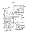
- the image signal receiving unit 30 is formed by a synchronizing signal detector (abbriviated as SYC DET in the figure), which detects the synchronizing signal SYC from the signal received by the modem 10 and produces a predetermined output as described in detail later.
- a reference numeral 302 denotes an AND gate
- a reference numeral 303 indicates a re-timing circuit which extracts the clock signal from the image signal received by the modem 10.
- a reference numeral 304 denotes a control signal generator which is composed of a counter (abbriviated as CNTR in the figure) 305 and a frequency divider 306.
- Reference numerals 307 to 312 represent 8- bit shift registers, and a reference numeral 313 denotes a changeover switch having a moving contact 314 and two fixed contacts 315 and 316. Further, the same reference numerals or characters as those used in Fig. 1 indicate the same component parts as shown in that figure. References attached to connecting lines will be referred to in the following explanation.
- the modem 10 (Fig. 1) is connected to the shift register 309 through a line N l .
- a line N 2 provides connection between the shift registers 309 and 308, and a line N 3 connects the shift registers 308 and 307.
- the shift register 307 is connected to the shift register 310 through lines N 4 .
- the shift register 308 is connected to the shift register 311 through lines N 5 .
- the shift register 309 is connected to the shift register 312 through lines N 6 .
- a line N 7 connects the shift register 310 and the decoder 61 (Fig. 1).
- the shift register 311 is connected to the decoder 62 through a line Ng.
- the shift register 312 is connected to the moving contact 314 of the changeover switch 313 through a line Ng.
- the fixed contact 315 of the changeover switch 313 is connected to the image memory 73 (Fig. 1) through a line N 10 and the other contact 316 to the image memory 74 through a line N 11 ⁇
- a line N 12 connected to the modem 10 (Fig. 1) is connected to one of the input terminals of the AND gate 302.
- the synchronizing signal detector 301 connected to the line N 12 is connected with the other input terminal of the AND gate 302.
- the re-timing circuit 303 connected with the output terminal of the AND gate 302 is connected to the shift registers 307, 308 and 309 through a line N 13 and-with the control signal generator 304 through a line N 14 .
- the control signal generator 304 the signal sent through the line N 14 , which is the clock signal reproduced by the re-timing circuit 303, is counted by the counter 305, so that control signals C E and C R are generated in accordance with the content of the counter 305.
- the control signal C R is sent to the shift registers 310 to 312 through a line N 15 , and the control signal C E is led to the changeover switch 313 through a line N 17 .
- the control signal C E functions as a changeover signal which repeatedly changes the connection of the moving contact 314 with the fixed contacts 315 and 316 in a predetermined period.
- the frequency divider 306 reduces the frequency of the clock signal down to one third. Namely, the frequency divider 306 produces one output pulse every three pulses of. the clock signal, and the output pulse is led to the shift registers 310 to 312 as a control signal C Q through a line N 16 .
- control signal generator 304 has the function of generating various kinds of control signals C R , C Q , C E at respectively predetermined timings on the basis of the reproduced clock signal. Therefore, it will be easily understood by one ordinarly skilled in the art that such a control signal generator also is constructed by a microcomputer which is so programmed as to generate the control signals in the manner as described above.
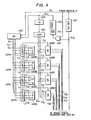
- This unit 40 is equipped with a synchronizing signal detector (abbriviated as SYC DET in the figure) 401, an AND gate 402, a re-timing circuit 403 which has the same function as the re-timing circuit 303 in Fig.
- a 1/8 frequency divider 404 a counter (abbriviated as CNTR) 405, a shift register (abbriviated as SR) 406, comparators (abbiriviated as COMPTR) 407A, 407B, 407C and 407D, shift registers (similarly abbriviated as SR) 408A, 408B, 408C and 408D, and code establishing circuits 409A, 409B, 409C and 409D, which have the same structure as those 213A to 213D of Fig. 2 and produce the output signals (code) corresponding thereto, respectively.
- the same reference numerals used in Fig. 1 indicate the same component parts as shown in that figure. References attached to connecting lines will be referred to in the following description.
- the modem 12 (Fig. 1) is connected to the shift register 406 through a line E l .
- Lines E 2 , E 3 and E 4 connected to the shift register 406 are connected to the comparators 407A to 407D.
- Lines L l , L 2 and L 3 connect the code establishing circuit 409A with the comparator 407A.
- lines L 4 to L 6 connect the code establishing circuit 409B with the comparator 407B.
- lines L 7 to Lg connect the circuit 409C with the comparator 407C and lines L 10 to L 12 connect the circuit 409D with the comparator 407D.
- comparators 407A to 407D have their respective output terminals connected to the shift registers 408A to 408D through lines E 5 to E 8 , respectively.
- the AND gate 402 has two input terminals, one being connected to the line E l through a line Eg and the other to the synchronizing signal detector 401 through a line E 10 .
- An output terminal of the AND gate 402 is connected to the re-timing circuit 403.
- the re-timing circuit 403 is connected with the frequency divider 404 and the shift register 406 through a line E ll . Lines E 12 to E 14 connected to the counter 405 are led to the shift registers 408A to 408D.
- Three lines E 15 are connected to the shift register 408A, three lines E 16 to the shift register408B, three lines E 17 to the shift register 408C, and three lines E 18 to the shift register 408D. These four sets of three lines E 15 to E 18 and the line E 10 are led to the image signal transmitting unit 50.
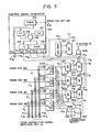
- Fig. 5 there is shown the structure of the image signal transmitting unit 50,. which comprises shift registers (abbriviated as SR in the figure) 501 to 506 and 511, an OR gate 508, a changeover switch 507 having a moving contact and two fixed contacts 509 and 510 as the changeover switch 313 (Fig. 3), a synchronizing signal memory (abbriviated as SYC MEM) 512 which is similar to the memory 210 (Fig. 2), selecting switch circuits 513A, 513B 513C and 513D, and a control signal generator 514.
- the control signal generator 514 has a timer 515 initiated by the synchronizing signal SYC from the detector 401 (Fig.
- the control signal generator 514 has the function of generating various kinds of timing and control signals C L , Cpi, Cp 2 , Cw, C T and Cu at respectively predetermined timings as mentioned later, initiated by the synchronizing signal SYC. Therefore, similarly to a case of the control signal generator 304 in Fig. 3, this control signal generator also can be constructed by a microcomputer which is so programmed as to generate the timing and control signals in the manner as described above. Further, the same reference numerals as used in Figs. 1 and 4 indicate the same component parts as shown in those figures. References attached to connecting lines will be referred to in the following.
- the switch circuit 513A has a movable contact connected to the coder 18A (Fig. 1) through a line F l .
- the switch circuit 513B has a movable contact connected to the coder 18B through a line F 2 .
- the switch circuit 513C has a movable contact connected to the coder 18C through a line F 3 .
- the switch circit 513D has a movable contact connected to the coder 18D through a line F 4 .
- a line F 5 connected to respective fixed contacts 1 of the switch circuits 513A to 513D is led to the shift register 501.
- a line F 6 connected to respective fixed contats 2 of the switch circuits 513A to 513D is led to the shift register 502.
- a line F 7 connected to respective fixed contats 3 of the switch circuits 513A to 513D is led to a fixed contact 509 of the changeover switch 507.
- a line F 8 connected to respective fixed contacts 4 of the switch circuits 513A to 513D is led to the other fixed contact 510 of the changeover swith 507.
- a line Fg connected to the movable contact of the changeover switch 507 is led to the shift register 503.
- the shift registers 501 and 504 are connected to each other through lines F 10
- the shift registers 502 and 505 are connected to each other through lines F ll
- the shift registers 503 and 506 are connected to each other through lines F 12 . Further, the.
- shift registers 504 to 506 are connected in series with one another through lines F 13 .
- the shift register 504 has an output terminal connected to one of the input terminals of the OR gate 508 through a line F 14 .
- This OR gate 508 has an output terminal connected to the modem 12 (Fig. 1).
- a line F 15 connected to the control signal generator 514 is led to the cameras 16A to 16D (Fig. 1) and the shift register 511.
- a line F 16 provides connection between the shift registers 501 to 503 and the control signal generator 514.
- a line F 17 from the control signal generator 514 is led to the shift register 511.
- Lines F 18 and F l g from the control signal generator 514 are both connected with the shift registers 504 to 506.
- the control signal generator 514 and the changeover switch 507 are connected to each other through a line F 20 .
- the lines E 15 to E 18 connected to the shift registers 408A to 408D of the instruction signal receiving unit 40 (Fig. 4), respectively, are connected to the selecting switch circuits 513A to 513D. In response to the signal sent through the corresponding one of the lines E 15 to E 18 , each movable contact of the selecting switch circuits 513A to 513D selects one contact among the fixed contacts 1 to 4.
- the timer 515 starts counting of time upon receipt of the signal from the synchronizing signal detector 401 (Fig. 4) and produces an output signal after the period corresponding to the duration in which the logic operation in the instruction signal receiving unit 40 is completed and thereby the signals of the lines E 15 to E 18 are produced.
- This output signal of the timer 515 becomes the signal C T sent to the cameras 16A to 16D (Fig. 1) and the shift register 511 through the line F 15 .
- the timer 515 produces a further output at the predetermined time after production of the signal C T .
- Another output of the timer 515 becomes the signal C U led to the changeover switch 507 as a changeover signal through the line F 20 .
- the flip-flop circuit 516 When the timer 515 produces the signal C T , the flip-flop circuit 516 is set, so that the clock signal from the clock oscillator 517 is given to the 1/3 frequency divider 519 and the counter 520 through the AND gate 518.
- the clock signal whose frequency is reduced down to one third is led to the shift registers 501 to 503 as the signal Cw through the line F 16 .
- the counter 520 counting the clock signal produces the signals C L , Cp l and C P2 in accordance with its content.
- the signals C L and Cp 2 are led to the shift registers 504 to 506 through the line F 19 and F 18 , respectively, and the signal Cp l to the register 511 through the line F 17 .
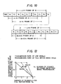
- Fig. 6 shows the states in which the shift registers 203 to 206 are being stored with the respective codes by turning on the switches 2A, 2C, 2B and 2D.
- the duration denoted by T l indicates the state before the switches are depressed (i.e., while all the switches are open), in which the shift registers 203 to 206 are stored with the value "0".
- the duration denoted by T 2 shows the state after the switch 2A is turned on whereas the remaining switches are left opoen, in which the shift register 203 is stored with the code "A".
- the duration denoted by T 3 shows the state after the switch 2C is turned on whereas the remaining switches are all turned off, in which the shift register 204 is stored with the code "A” whereas the shift register 203 is stored with the code "C”.
- the duration denoted by T 4 indicates the state after the switch 2B is turned on whereas the remaining switches are turned off, in which the shift register 205 is stored with the code "A”, the shift register 204 with the code "C”, and the shift register 203 with the code "B".
- T 5 indicates the state after the switch 2D is turned on where as the remaining switches are all turned off, in which the shift registers 206, 205, 204 and 203 are stored with the codes "A”, “C”, "B” and "D", respectively.
- the order of the codes "A”, "B”, “C” and “D” stored in the shift registers 206 to 203 can be arbitratily changed by varying the order of manipulation of the switches 2A to 2D by the operator.
- This manipulation order has the significance in the assignment of transmission channels. Namely, in this embodiment, the frequency bandwidth of the transmission line 14 is divided into three transmission channels, and as is understood from the explanation described later, two of the three channels are assigned to the transmission of image signal for full motion images (called a full motion image transmission, hereinafter) and the remaining one channel to the image signal transmission for frame repetition images (called a frame repetition image transmission, hereinafter).
- This assignment of transmission channels is determined by the order of storing the codes "A" to "D" in the shift registors 206 to 203, that is to say, the order of manipulation of the switches 2A to 2D.
- the image signals picked up by the camera 16A and 16C which are at first selected can be transmitted by the full motion image transmission through two channels.
- the image signals picked up by the camera 16B and 16D are transmitted on the time-sharing basis through one channel as the frame repetition transmission.
- the switch 3 which has been left open, is turned on by the operator.
- the operation of the instruction signal transmitting unit 20 after operation of the switch 3 is explained, referring to Fig. 7.
- the monostable . multivibrator 207 outputs the signal which is shown in Fig. 7(b).
- the term during which the output signal of the multivibrator 207 is high, i.e. the so-called time constant of the multivibrator 207 is determined in dependence on the length of the instruction signal described later in reference to Fig. 7(f).
- the lock signal oscillator 208 outputs the clock signal which is shown in Fig. 7(c).
- the AND gate 209 outputs the signal which is shown in Fig. 7(d).
- the shift register 111 receives the ON signal of the switch 3 through the line K 18 to store the synchronizing signal SYC which is outputted from the memory 210.
- the pulse signal outputted from the AND gate 209 is transmitted through the lines K 13 and K 19 to the shift registers 203 to 206 and 211.
- these shift registers 203 to 206 and 211 conduct their shiftig operations. In Fig. 7(e), this operation is shown as a change of content of the register only with respect to the shift register 211.
- the synchronizing signal SYC and the codes stored in the shift registers 211, 206, 205, 204 and 203 are shifted and outputted from the shift register 211 to the modem 10 sequentially in the order as shown in Fig. 7(f).
- the code signal "D" last stored in the shift register 203, for example, is shifted in the order of the shift registers 204, 205, 206 and 211.
- the signal thus outputted from the shift register 211 to the line K 20 by those shifting operations becomes the instruction signal which is headed by the synchronizing SYC followed by respective one-byte signals set with the codes A, C, B and D, respectively as shown in Fig. 7(f).
- the shift registers 203 to 206 and 211, the multiple switches 212A to 212D and the code establishing circuits 213A to 213D have functions to prepare and output the instruction signals for assigning the full motion images and the frame repetition images.
- the codes stored in the shift registers 206 and 205 correspond to the full motion images whereas the codes stored in the shift registers 204 and 203 correspond to the frame repetition images, more specifically, the two codes A and C following the synchronizing signal SYC of the instruction signal are assigned to the full motion images whereas the subsequent two codes B and D are assigned to the frame repetition images.
- the generation of the instruction signal comprises the following steps. Namely,with a first step, the code signals assigned to the cameras equipped at the sites to be monitored are produced in accordance with the order of selection of the cameras, i.e. the order of manipulation of the push-button switches 2A to 2D. In a second step, the synchronizing signal SYC is attached to the head of the train of the code signals. Finally, the thus obtained instruction signal is sent to the modem 10. As is understood from this, the instruction signal can be attained by a microcomputer which is so programed as to execute the above steps.
- the instruction signal is transmitted through the transmission line 14 to the modem 12 of the side to be monitored and further to the instruction signal receiving unit 40.
- the explanation is done of the operation of the instruction signal receiving unit 40.
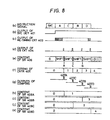
- the received instruction signal as shown in Fig. 8(a) is inputted to the synchronizing signal detector 401 and the shift register 406.
- the 401 detects the synchronizing signal SYC and outputs a signal which is shown in Fig. 8(b).
- the re-timing circuit 403 having received the output of the detector 401 through the AND gate .402 reproduces and outputs the clock signal which is shown in Fig. 8(c).
- the 1/8 frequency divider 404 divides the frequency of the reproduced clock signal to output the signal which is shown in Fig. 8(d).
- the counter 405 counts the output of the 1/8 frequency divider 404 to output the counted values as 1, 2, 3 and 4 sequentially, as shown in Fig. 8(f).
- the shift register 406 receives the reproduced clock signal through the lilne E 11 , and thereby the instruction signal is taken thereinto.
- the clock signal is not yet reproduced when the synchronizing signal SYC reaches the shift register 406. Accordingly, the synchro-nizing signal SYC is not taken into the shift register 406, but the register 406 inputs only the code signals A to D following to the synchronizing signal SYC bit by bit in response to the clock signal.
- the change of content of the shift register 406 is as shown in Fig. 8 (e) .
- the output of the counter 405 is led to all the shift registers 408A to 408D.
- the outputs of the comparators 407A to 407D are also led to the corresponding shift registers 408A to 408D as an input timing signal.
- the shift registers 408A to 408D input the content of the counter 405 at that time thereinto. Consequently, the shift registers 408A to 408D store the counted values, as shown in Figs. 8(h) to 8(k). In this embodiment, the counted values take 1, 3, 2 and 4, respectively.
- the counter 405, the comparators 407A to 407D and the shift registers 408A to 408D select the cameras for the full mostion images and the cameras for frame repetition images in response to the instruction signal mentioned above.
- the counter 405, the comparator 407A and the shift register 408A judge whether it is for the full motion or frame repetition images.
- the counter 405, the comparator 407B and the shift register 408B judge whether it is for the full motion or frame repetition images.
- the counter 405, the comparator 407C and the shift register 408C judge whether the camera 16C is for the full motion or frame repetition images.
- the counter 405, the comparator 407D and the shift register 408D judge whether the camera 16D is for the full motion or frame repetition images.
- the instruction receiving unit 40 discriminates the order of the code signals A to D included in the received instruction signal.
- this unit 40 has the function of decoding the instruction signal which comprises the following steps; generating the codes corresponding to the codes assigned to the cameras, comparing each of the thus generated codes with the successively received code signal one after another, and discriminating the order of reception of the code signals on the basis of the above comparison to produce a contact selecting signal to the selecting switch circuits. All of these steps can be achieved by a usual microcomputer, so that, similarly to the instruction signal transmitting unit 20 shown in Fig. 2, the instruction signal receiving unit 40 also can be constructed by a microcomputer which is so programed as to execute the above mentioned steps.
- the contents stored in the shift registers 408A to 408D are led to the image signal transmitting unit 50 through the lines E 15 to E 18 .
- the operation of the image signal transmitting unit 40 will be explained in the following, referring to Figs. 5 and 9.
- the signals which are led through the lines E 15 to E 18 are given to the selecting switch circuits 513A to 513D as the contact selecting signal, respectively.
- Each of these signals determines one of four fixed contacts to be selected by the movable contact.
- each of these signals carries one of the numerical values 1 to 4, the numerical value corresponds to the number of the fixed contact to be selected which is attached as shown in the figure. Accordingly, the signal transmitted through the line E 15 is led to the switch circuit 513A.
- This switch circuit 513A connects the movable contact to the fixed contact of the number 1 since the numerical value of this signal is 1.
- the selecting switch circuits 513A to 513D are switching means to connect the respective cameras with a full motion or a frame repetition image transmission means in accordance with the aforementioned camera selecting function of the instruction signal receiving unit 40.
- the image signal output from the cameras 16A to 16D is synchronized with the signal C T . as shown in Fig. 9(a), which is transmitted from the control signal generaor 514 through the line F 15 .
- the signal C T is outputted from the control signal generator 514 after the signals on the lines E 15 to E 18 have been produced.
- the signal C T is inputted through the line F 15 to the shift register 511.
- This shift register 511 receives and stores the synchronizing signal SYC from the memory 512.
- the image signals generated by the cameras 16A to 16D are sent to the coders 18A to 18D so that they become pixel signals which are shown in Figs. 9(f) to 9(i).
- the pixel signal outputted from the coder 18A is inputted to the shift register 501 through the lines F l and F 5 .
- the pixel signal outputted from the coder 18C is sent to the shift register 502 through the lines F 3 and F 6 .
- the pixel signal outputted from the coder 18B is transmitted to the changeover switch 507 through the lines F 2 and F 7 .
- the pixel signal outputted from the coder 18D is transmitted to the changeover switch 507 through the lines F 4 and F 8 .
- the changeover switch 507 has its movable contact connected alternately at a predetermined interval with the fixed contact 509 connected to the line F 7 and the fixed contact 510 connected to the line F 8 .
- This switching operation of the movable contact is conducted each time the image signals from the coders 18B and 18D are sent for one picture frame.
- This switching operation of the movable contact of the changeover switch 507 is conducted in response to the signal C U which is given from the control signal generator 514 to the changeover switch 507 through the line F 20 .
- the movable contact of the changeover switch 507 will be connected with the fixed contact 509.
- the pixel signal from the coder 18B is inputted to the shift register 503.
- the storage of the pixel signals in the shift registers 501 to 503 is conducted in synchronism with the signal C W as shown in Fig. 9(e), which is outputted from the control signal generator 514 after the signal C T takes the value "0".
- a signal C L shown in Fig. 9 (d) is inputted to the shift registers 504 to 506
- pixel signals A 1 , C l and B l stored in the shift registers 501 to 503 are transferred to and stored in the corresponding shift registers 504 to 506 (as shown in Figs. 9(k) to 9(m).
- the shift registers 501, 502, 504 and 505 are storage means for the full motion images.
- the switching circuit 507 and the shift registers 503 and 506 form storage means for the frame repetition images.
- a signal Cp l is outputted from the same, as shown in Fig. 9(b).
- the shift register 511 receives the signal Cp l through the line F 17 to output the stored synchronizing signal SYC to the modem 12 through the OR gate 508.
- the signal C P1 is interrupted simultaneously with the interruption of the signal C L .
- a signal Cp 2 is outputted from the control signal generator 514.
- the signal Cp 2 is inputted to the shift registers 504 to 506, the pixel signals A 1 , C l and B l stored in those shift registers are sent out in series to the modem 12 through the OR gate 508.
- an image signal headed by the synchronizing signal SYC as shown in Fig. 9(p) is outputted from the madem 12 to the transmission line 14.
- FIG. 10 The detail of the image signal outputted from the modem 12 is shown in Fig. 10.
- This figure shows the formation of the image signal of k-th and (k+l)th frames with respect to the images A and C picked up by the cameras 16A and 16C which are both transmitted by the full motion image transmission and a j-th frame with respect to the images B and D picked up by the cameras 16B and 16D which are transmitted by the frame repetition image transmission.
- the pixel signals A 1 , C 1 and B l are outputted from the shift register 504, they are accompanied by successive pixel signals A 2 , C 2 and B 2 until pixel signals An, C n and B n are finally outputted.
- the pixel signals A 1 to An construct one frame of the image A
- the pixel signals C 1 to C n construct one frame of the image C
- the pixel signals B l to B n construct one frame of the image B.
- the movable contact of changeover switch 507 is connected with the fixed contact 510 thereof, so that the pixel signal D 1 is stored in the shift register 503 and further in the shift register 506.
- the pixel signals A 1 , C 1 , D 1 , A 2 , C 2 , D 2 and so on are outputted sequentially in the same manner as described above.
- An variation of assignment of channels to the full motion image and the frame repetition image transmissions can be achieved by changing the wiring between the selecting switch circuits 513A to 513D and the shift registers 501, 502 and' the changeover switch 507. If a changeover switch having three fixed contacts is substituted for the two-fixed-contact changeover switch 507 as used in Fig. 5 and the line F 6 is connected to a third fixed contact thereof, it can be realilzed that only one channel is assigned to the full motion image transmission, and the remaining two channels are employed for the frame repetition image transmission.
- the transmission line 14 is divided into .' more than three channels, there must be provided the number of selecting switch circuits corresponding to the number of channels.
- the number of fixed contacts of each of such selecting switch circuits also must corespond to the number of the channels.
- the number of fixed contacts of the changeover switch is determined in dependence on how many channels are assigned to the full motion image transmission. For example, in the case where the transmission line is divided into 50 channels and two channels thereamong are assigned to the full motion image transmission, 48 fixed contacts is necessary in the changeover switch.
- the wiring between the selecting switch circuits and the changeover switch can be easily done in accordance with the same way as that shown in Fig. 5.
- the arrangement of the shift registers 501 to 506 does not change, since two channels are assigned to the full motion image transmission in the same manner as in Fig. 5 and the single shift register for storing the image signal of the frame repetition image is used by changing the image signals of every frame repetition image transmissions.
- the above mentioned image signal obtained in the image signal transmitting unit 50 is sent from the modem 12 through the transmission line 14 to the monitor room and received by the modem 10.
- the description will be made of the operation of the image signal receiving unit 30 which is supplied with the image signal received by the modem 10, referring to Figs. 3 and 11.
- the image signal received by the modem 10 is inputted to the shift register 309 through the line N 1 and the synchronizing signal detector 301 through the line N 12 .
- This synchronizing signal detector 301 receives the image signal as shown in Fig. 11(a) to output a signal as shown in Fig. 11 (b). This output is inputted through the AND gate 302 to the re-timing circuit 303.
- This circuit 303 outputs a clock pulse signal which is shown in Fig. 11(c).
- This pulse signal is inputted to the control signal generator 304 as well as to the shift registers 307 to 309. As a result, these shift registers 307 to 309 take in the pixel signals A 1 , C 1 and B l .
- the shift register 307 takes in the pixel signals (A l , A 2 , . ., and An) pixel by pixel, as shown in Fig. 11(e).
- the shift register 308 takes in the pixel signals (C l , C 2 , . , and C n ) pixel by pixel, as shown in Fig. 11(f).
- the shift register 309 takes in the pixel signals (B 1 , B 2 , across, and B n ) pixel by pixel, as shown in Fig. 11 (g).
- the synchronizing signal SYC included in the received image signal is not taken into the shift register 307 to 309, since the clock signal is not yet reproduced when the synchronizing signal SYC reaches the shift register 309.
- a signal C R (as shown in Fig. 11(d)) is outputted from the control signal generator 304 and inputted to the shift registers 310 to 312.
- the shift registers 310 to 312 take in and store the pixel signals A 1 , C l and B l stored in the corresponding shift registers 307 to 309, as shown in Figs. 11 (h) to (j).
- a signal C Q (as shown in Fig. 11(k)) outputted from the control signal generator 304 is led to the shift registers 310 to 312. At this time, the shift registers 310 to 312 output the pixel signals stored therein.
- the pixel signals (A 1 , A 2 , . ., and An) outputted sequentially from the shift register 310 are sent as the image signal to the decoder 61.
- the decoder 61 decodes and decompresses the digital, bandwidth-compressed image signal, so that the monitor television set 81 displays the image which has been taken by the camera 16A.
- the pixel signals (C l , C 2 , . , and C n ) outputted from the shift register 311 are sent as the image signal to the decoder 62.
- the decoder 62 decodes and decompresses the digital, bandwidth-compressed image signal, so that the monitor television set 82 displays the image which has been taken by the camera 16C.
- the changeover switch 313 receives the signal C E (as shown in Fig. 11(p)) outputted from the control signal generator 304 and has its movable contact 314 connect with the fixed contact 315.
- the pixel signals (B 1 , B 2 , ., and B n ) outputted from the shift register 312 are once stored in the memory 73.
- the pixel signals stored in the memory 73 are led to the decoder 63, in which they are decoded and decompressed, so that the monitor television set 83 displays the image which has been taken by the camera 16B.
- the movable contact 314 is so controlled by the signal C E that it is connected with the fixed contact 315, when the movable contact of the changeover switch 507 (Fig.
- the image signals displayed by the monitor television sets 81 and 82 are transmitted continulusly form the side to be monitored at all times whereas the image signals displayed by the monitor television sets 83 and 84 are transmitted alternately for each picture frame, i.e., at a slow speed.
- the monitor television sets 81 and 82 are used for monitoring the sites where the states of the objects being monitored are subject to instantaneous and drastic change.
- the monitor television sets 83 and 84 can be utilized for monitoring the sites where the states of the objects being monitored are less likely to change.
- the memories 73 and 74 store the image signal for the slow- speed images. As a result, even when no image is transmitted for a while, the monitor television sets 83 and 84 display the images stored in the memories 73 and 74.
- the transmission line has the capability of the transmission rate of 96 Mbps, and by using the appropriate bandwidth compression method, e.g. a two- dimensional predictive coding scheme, the image signal is compressed to a digital signal of 4 bits per pixel.
- the frequency bandwidth required of the transmission line corresponds to 32 Mbps (4MHz X 2 X 4 bits). Therefore, the transmission line with the capability of 96Mbps as mentioned above can be divided 'into 3 transmission channels, each having the equal rate of 32 Mbps.
- one frame of picture is composed of 512 X 512 pixels, which correspond to about 1049 K bits in the digital image signal.
- the transmission channel having the transmission rate of 32 Mbps the time necessary for completing the transmission of one frame becomes about 33 msec (1049 K bits - 32Mbps). Accordingly the image signals for about 30 frames can be transmitted every one second through one transmission channel. If two channels, i.e. the capability of 64Mbps, are used, the image signals for 60 frames can be transmitted every one second, and further, those for 90 frames can be transmitted in a case of three channels, i.e. by using the full capability (96 Mbps) of the transmission line. Actually, however, 32 Mbps, i.e. 30 frames per second, is the rate enough to reproduce the full motion image in the receiving side.
- the reproduction of the full motion image of a certain site to be monitored becomes possible, if the image signals of the certain site can be transmitted at the rate of 30 frames/sec. Therefore, more than one channel is not necessary to be assigned to the full motion image transmission of one site to be monitored.
- two channels of the line which is divided into three transmission channels are assigned to the full motion image transmission for two sites which are monitored by the cameras 16A and 16C, and the remaining one transmission channel is used for the fram repetition image transmission for two sites which are sensed by the cameras 16B and 16D.
- one channel having the capability of 30 frames/sec is exhausted for the frame repetition image transmission for only two sites to-be monitored. Therefore, the capability of the transmission rate of 15 frames/sec is assigned to each site to be monitored.
- the transmission rate of 15 frames/sec/site is extremely high for the frame repetition image transmission and does not result in the effective utilization of the transmission line.
- the transmission rate of 1 frame/sec/site is usually sufficient for the frame repetition image transmission, although, of course, that depends on the field in which the image transmission system of this kind is used. If the transmission rate is set at such a value as 1 frome/sec/site, it becomes possible to transmit the image signals for 30 sites every one second through one transmission channel by assigning each one of 30 frames to each one of 30 sites. Further, if the reduction of the transmission rate, e.g. down to 0.5 frames/sec/site, is allowed, the image signals for 60 sites to be monitored can be transmitted every one second through one transmission channel.
- Fig. 12 plots the relation between the transmission rate of the frame repetition image (frames/sec/site) and the number of channels assigned to the full motion image transmission (N M ) as mentioned above, in which the number of frames by the frame repetition image transmission is rended a parameter.
- N M the number of channels assigned to the full motion image transmission
- the operator can ⁇ change the display of the image of the site in question from the frame repetition image to 'the full motion image by .manipulating the push-button switches 2A to 2D (Fig. 1). Namely, if it has been found from the display of the monitor television set 84, which is in the frame repetition image, that there occurs an abnormal state in the site monitored by the camera 16D, the operator re-manipulates the push-button switches so that the switch 2D is at first pushed, preceding to the manipulation of the other push-button switches. Consequently, the image signal picked up by the camera 16D is transmitted by the full motion image transmission.
- the effect can be attained which provides a system in which the channel or channels can be preferentially assigned to the monitoring operations of the sites having high importance or emergency by means of the full motion images whereas the remaining channels can be assigned to the monitoring operations of the remaining sites by means of the frame repetition images, so that the limited capacity of the transmission line can be effectively utilized and that the system can be suitably applied for monitoring such an object having hundreds of sites to be monitored as the big plant or building.
- the monitor television sets which display the full motion images the image transmission period is so short that the monitoring operations can be conducted almost in a real time base.
- the transmission period for the image of each 'of them is long, but the images of a number of TV cameras can be monitored.
- the portions of the image signal transmitting unit 50 to be stored with the image signals of the frame repetition images have their structures simplified because of the limited number of shift registers.
- the portions (e.g., the shift registers 309 and 312) to be stored with the image signals of the frame repetition images have their structures simplifiled. Since the image signals of the plural cameras for the frame repetition images are stored alternately in one image storage, the structures of the storages for the frame repetition images can be simplified so that the structures of the respective unit can be simplified.
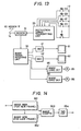
- FIG. 13 Another embodiment of the present invention is shown in Fig. 13.
- the same refer-ence characters as those of the embodiment of Fig. 1 indiate the same parts.
- reference numerals 95 and 96 indicate image change detection circuits and reference numerals 85 and 86 alarm lamps.
- the image change detection circuit 95 or 96 has such a structure as is shown in Fig. 14.
- a reference numeral 951 indicates an image memory to be stored with the frame of this time, e.g., 512 512 picture elements
- a reference numeral 952 an image memory to be stored with the last frame
- a reference numeral 953 an image comparator to compute the sum of the difference between the pixel values of the memories 951 and 952.
- a reference numeral 954 indicates a threshold circuit which generates an output, when the sum of the difference of the pixel values of the comparator 953 exceeds a predetermined value, causing the alarm lamp 85 or 86 to light.
- the operator watches the monitor television sets 81 and 82 for full motion images. If the alarm lamp 85 or 86 lights during the automatic watch of the image changes by the circuit 95 and 96 for the frame repetition images, the image sensed by the cameras 16A to 16D corresponding to the alarming lamp 85 or 86 can be displayed on the image minotor television set 81 or 82, by remanipulating the switches 2A to 2D and 3. Further, by cooperating the operation of the switches 2A to 2D and 3 with the outputs of the image change detection circuits 95 and 96, the monitor television set 81 or 82 can be automatically switched to display the image picked up by the camera 16A to 16D corresponding to the alarming lamp 85 or 86.
Abstract
Description
- The present invention relates to an image transmission system and more particularly to an image transmission system suitably applied to such a monitoring system for a plant or a security system for a building that has a lot of sites to be monitored or watched so that the large amount of image information is exchanged between a monitor room side and a side of the sites to be monitored or watched through a transmission line.
- Monitoring systems for various kinds of plants, security systems of premises and the like employ an image transmission technique. Usually, an image transmission system for such use is constructed as follows. Namely, there are provided a plurality of television cameras in sites to be monitored or watched. The image signal outputted by a television camera is digitized by a coder, which has functions of bandwidth compression as well as coding, and multiplexed with digitized signals from other cameras in a multiplexer. The multiplexed image signals are sent out on a transmission line on the time-sharing basis.
- In a monitor room located apart from the sites equipped with the cameras, there is provided a demultiplexer, which demultiplexes the image signals sent from the sites to be monitored. The demultiplexed image signal is decoded by a decoder and displayed on a corresponding monitor television set. Thereby, an operator in the monitor room can watch current states or occurrences in the plural sites within a plant or building. In such an image transmission system, it is required to be able to transmit image information from the cameras in a real-time. Further, it is most preferable that malfunction of plant elements and unusual occurrence within a building can be watched by full motion image on the monitor television set.
- Here, let us consider a case of a monitoring system where television cameras are provided in 50 sites of a plant to be monitored. If the image signal from each camera is converted into a digital signal of 8 bits and such a digital signal is transmitted in a base frequency of 4 MHz, the transmission rate required of a transmission line becomes as follows:
50 x 4 MHz x 2 X 8 bits = 3.2 Gbps wherein the sampling for coding the image signal depends' on the Shannon's sampling theorem. - At present, it is very difficult to realize a transmission line having a band width as estimated above. At least, it can be said that it is almost impossible to realize such a transmission line commercially. On the other hand, 50 sites to be monitored are not so much, compared with cases of usual plants. Further, in a security system of a big building, the number of sites to be watched will become much larger.
- An object of the present invention is to provide an image transmission system which can effectively utilize the limited transmission capability of a transmission line connecting between a side from which image information is sent out and a side in which it is received and enables a necessary image information to be transmitted on the real time basis.
- A fundamental feature of the present invention is in that the image informations to be transmitted are divided into those of the high degree of demand, i.e. important image informations, and other image informations, one transmission channel of the transmission line which is divided into plural channels is assigned for the transmission of each of the important image informations, and the other image informations are transmitted on the time-sharing basis through the remaining channels of the transmission line.
- More specifically, in case an image transmission system according to the present invention is applied to such a monitoring system of a plant or a seculilty system of a building that includes a monitored side with a lot of sites to be monitored or watched, each site having a television camera for sensing an image of the site, a monitoring side equipped with monitors by which the images of the sites can be monitored or watched and a transmission line connecting therebetween, the frequency bandwidth of which is divided into plural transmission channels, an instruction signal is produced by an operator in the monitoring side, which includes a code signal in which a code assigned to each of the television cameras is arranged in the order selected by the operator. A first group of codes within the arrangement of codes is so designated that image signals picked up by the cameras assigned the codes are transmitted as full motion imges, and - a second group consisting of the remaining codes is so designated that image signals picked up by the cameras assigned the remaining codes are transmitted as frame repetition images. In accordance with such an instruction signal, there is produced in the monitored side an image transmission signal which is so formed that, to the transmission of each of the image signals picked up by the cameras assigned the codes of the first group, one of the plural transmission channels is assigned and all of the image signals picked up by the cameras assigned the codes of the second group are multiplexed on the time-sharing basis and transmitted through the remaining transmission channels.
- According to the present invention, the images of the important sites can be monitored or watched on the real time basis with the full motion images and the images of the remaining sites are monitored or watched with the frame repetition images, so that the transmission capability of the transmission line can be considerably saved, compared with the case where the capability of the transmission line is equally shared to the transmission of the image signals picked up by all the cameras.
- Further, when a malfunction or abnormal state occurs in the site which has been monitored by the frame repetition images till then, the image of the site can be changed td the full motion images by reissuing the instruction signal such that the code of the camera sensing the site in question belongs to the first group of codes. Thereby, the malfunction or abnormal state occuring in the site can be monitored in detail on the real time basis.
-
- Fig. 1 shows an overall structure of an image transmission system according to an embodiment of the present invention, which is applied to a monitoring system in a plant or a security system for a building;
- Fig. 2 is a block diagram showing a . detailed structure of an instruction signal transmitting unit used in the embodiment of Fig. 1;
- Fig. 3 is a block diagram showing a detailed structure of an image signal receiving unit used in the embodiment of Fig. 1;
- Fig. 4 is a block diagram showing a detailed structure of an instruction signal receiving unit used in the embodiment of Fig. 1;
- Fig. 5 is a block diagram showing a detailed structure of an image signal transmitting unit used in the embodiment of Fig. 1;
- Fig. 6 is an explanatory chart showing the states of storing the signals in shift registers included in the instruction signal transmitting unit show in Fig. 2;
- Fig. 7 is an explanatory chart showing the operation of the instruction signal trnsmitting unit shown in Fig. 2;
- Fig. 8 is an explanatory chart showing the operation of the instruction signal receiving unit shown in Fig. 4;
- Fig. 9 is an explanatory chart showing the operation of the image signal transmitting unit shown in Fig. 5
- Fig. 10 shows a detailed formation of an image signal outputted from the image signal transmitting unit shown in Fig. 5;
- Fig. 11 is an explanatory chart showing the operation of the image signal receiving unit shown in Fig. 3;
- Fig. 12 is a characteristic chart for explaining the effect of the embodiment shown in Fig. 1, in which the relation between the number of channels for the full motion image and the transmission rate of the frame repetition image is plotted with the number of frames by the frame repetition image transmission as a parameter;
- Fig. 13 shows a part of a structure of an image transmission system according to another embodimenbt of the present invention; and
- Fig. 14 is a block diagram showing a structure of an image change detection circuit used in the another embodiment shown in Fig. 13.
- Fig. 1 is a schematic diagram showing an overall construction of an image transmission system according to an embodiment of the present invention. Referring at first to a right half of the figure, an arrangement of elements in a monitor room is schematically illustrated, which includes an instruction
signal transmitting unit 20 and an imagesignal receiving unit 30.. To the instructionsignal transmitting unit 20, signals which are produced byswitches switches 2A to 2D can be push-button switches, for example, and hence each switch produces an output signal only during the operator pushes it. Further, the operator may not manipulate more than one among theswitches 2A to 2D simultaneously, because, as is apparent from the description later, the conflict occurs among signals produced by the switches pushed simultaneously. In order to prevent such an inconvenience, there can be provided an electrical or mechanical lock mechanism which inhibits a switch from being pushed when another switch is manipulated. As theswitch 3, a push-button switch, a knife switch or other type switches can be used. - The image
signal receiving unit 30 gives received image signals to decoders (abbriviated as DEC in the figure) 61, 62, 63 and 64, however twodecoders signal receiving unit 30 in the bandwidth-compressed form, thedecoders 61 to 64 are necessary to have the function of decompression of the image signals, in addition to the functions of decoding of coded signals and conversion from digital signals to analog signals a decoder of the usual type has. Such a decoder can be easily realized by the combination of known devices. Theimage memories - The image signal which is decompressed, decoded and converted into the analog signal in each
decoder 61 to 64, is led to a correspondingmonitor television set - The instruction
signal transmitting unit 20 and the imagesignal receiving unit 30 are connected to amodem 10, to which theformer unit 20 sends the instruction signal and from which thelatter unit 30 receives the image signal. - On the other hand, in a left half of Fig. 1, an arrangement of a side to be monitored or watched is schematically shown, wherein there are provided an instruction
signal receiving unit 40 and an imagesignal transmitting unit 50 which are both connected to amodem 12. Themodem 12 is connected to themodem 10 of the monitor room side through atransmission line 14. - The instruction signal which is produced in the instruction
signal transmitting unit 20 and received by themodem 12, is led to the instructionsignal receiving unit 40, which generates various kinds of timing and control signals in accordance with the received instruction signal. These signals generated by theunit 40 are given to the imagesignal transmitting unit 50. The timing signal among them is also led to television cameras (abbriviated as CAMR in the figure) 16A, 16B, 16C and 16D which are equipped at sites or locations to be monitored or watched in the plant or building. Each of thecameras 16A to 16D picks up an image of a subject or area assignd thereto for observation to output the image signal in response to the timing signal. Although fourcameras 16A to 16D are indicated in the figure, there is no limitation in the number of equipped cameras. - The image signals outputted from the
cameras 16A to 16D are led to corresponding coders (each abbriviated as COD in the figure) 18A, 18B, 18C and 18D. Each of thecoders 18A to 18D has a function of bandwidth compression, in addition to functions of conversion from analog signals to digital signals and coding of converted signals as an usual coder has. Similarly to thedecoders 61 to 64 of the monitor room side, a coder of such a type as described above can be formed by combination of known devices. - The coded image signals are given to the image
signal transmitting unit 50, in which the processing for transmission is executed on the image signals, and thereafter the processed image signal is sent to themodem 12. - Here, the following should be understood in connection with the arrangement of the side to be monitored or watched. Namely, Fig. 1 shows the case where a plurality of the
cameras 16A to 16D equipped at the sites arbitrarily selected for observation of the plant or building are controlled by a single pair of the instructionsignal receiving unit 40 and the imagesignal transmitting unit 50. However, it can be considered that the large number of cameras are divided into several groups and the pair of theunits 40 and 50 (including the modem 12) is prepared for every camera groups. The arrangement in each group is quite the same as that shown in Fig. 1, and in this case the pairs of theunits units modem 10 of the monitor room through an appropriate transmission line. To this end, for example, a known loop-formed transmission line can be used, by which every modems including themodem 10 are connected. - Next, the description will be made of the detailed structure of the
units - At first, the detailed structure of the instruction
signal transmittting unit 20 is shown in Fig. 2.Reference numerals reference numerals reference numeral 207 indicates a monostable multivibrator (abbriviated as MNSTBMV in the figure), a numeral 208 a clock signal oscillator (abbriviated as CLK in the figure), and a numeral 209 an AND gate. Areference numeral 210 indicates a memory stored with the code of a synchronizing signal SYC (abbriviated as SYC MEN in the figure). -
References comeras 16A to 16D. The codes produced by the circuits 213A to 213D correspond to thecomeras 16A to 16D, respectively. Therefore, if there are provided more cameras, code establishing circuits are prepared in accordance with the number of the cameras. It is of couse that push-buttom switches, multiple switches and shift registers must be increased accordingly. However, it will be understood that the way of connecting these increased elements does not change in spite of increase of the number of cameras. Especially, if the number of cameras is equal to or less than seven, it is sufficient that further three code establishing circuits which are coded as "101", "110" and "111", respectively, are connected in parallel with the lines K5 to K7 through multiple switches provided correspondingly thereto and three shift registers are connected in cascade with the shift registers 203 to 206. Further three push-button switches must be provided to actuate the newly provided multiple switches. If the number of cameras exceeds seven, the code of three digits becomes insufficient for assigning the code to every cameras. In that case, a code establishing circuit which can generate the code of more than three digits is used. -
References - Each of the
multiple switches 212A to 212D is equipped with three contacts which are connected to theshift register 203 through lines K5, K6 and K7. Lines Ll, L2 and L3 connected to the three contacts of themultiple switch 212A are connected to the code establishing circuit 213A. In this circuit 213A, the lines L1, L2 are connected to ground whereas the line L3 is connected to the positive voltage source +V. As a result, the code A is expressed in the form of three digit signal "001". Lines L4, L5 and L6 are connected to the three contacts of themultiple switch 212B, respectively. In thecode establishing circuit 213B, the lines L4, L6 are connected to ground whereas the lilne L5 is connected to the positive voltage source +V. As a result, the code B is expressed in the form of three digit signal "010". In thecode establishing circuit 213C, a lilne L7 connected to ground and lines L8 and Lg connected to the positive voltage source +V are connected with the three contacts of themultiple switch 212C, respectively. The code C, therefore, is expressed in the form of three digit signal "011". In thecode establishing circuit 213D, a line L10 connected with the positive voltage source +V and lines L11 and L12 connected to ground are connected with the three contacts constituting themultiple switch 212D, respectively. The code D is expressed in the form of three digit signal "100". The shift registers 203 and 204 are connected with each other through three lines K14. Three lines K15 connect the shift registers 204 and 205. The lines K16 connect the shift registers 205 and 206. Remaining terminals of the 8-bit shift registers 203 to 206 are connected in cascade and grounded. Namely, a dummy of 5 bits each having the logical value of zero is added to the 3-bit signal generated by the code establishing circuits 213A to 213D. Further, theshift register 206 is connected to theshift register 211 through a line K17. - A line Kl connects the
switch 2A and themultiple switch 212A. A line K2 connects theswitch 2B and themultiple switch 212B, a line K3 connects theswitch 2C and themultiple switch 212C, and a line K4 connects theswitch 2D and themultiple switch 212D. Theswitches 2A to 2D are connected with theOR gate 201 through lines K8, Kg, K10 and K11, respectively. The ORgate 201 has its output terminal connected to theOR gate 202 through a line K12. The ORgate 202 has its output terminal connected to the shift registers 203 to 206 through a line K13. Theswitch 3 is connected to themonostable multivibrator 207 and theshift register 211 through a line K18. Themonostable multivibrator 207 and theclock signal oscillator 208 are connected to the input terminal of the ANDgate 209. This ANDgate 209 has its output terminal connected to the input terminal of theOR gate 202. The ANDgate 209 is also connected to theshift register 211 through a line K19. TheSYC memory 210 is connected with between theshift register 211. A line K20 provides connection between theshift register 211 and themodem 10. - Referring next to Fig. 3, the detailed structure of the image
signal receiving unit 30 is explained hereinafter. - The image
signal receiving unit 30 is formed by a synchronizing signal detector (abbriviated as SYC DET in the figure), which detects the synchronizing signal SYC from the signal received by themodem 10 and produces a predetermined output as described in detail later. Areference numeral 302 denotes an AND gate, and areference numeral 303 indicates a re-timing circuit which extracts the clock signal from the image signal received by themodem 10. Such a technique that the clock signal is extracted and reproduced from the received signal itself is a well known technique in the field of data transmission. A reference numeral 304 denotes a control signal generator which is composed of a counter (abbriviated as CNTR in the figure) 305 and afrequency divider 306.Reference numerals 307 to 312 represent 8- bit shift registers, and areference numeral 313 denotes a changeover switch having a movingcontact 314 and two fixedcontacts - The modem 10 (Fig. 1) is connected to the
shift register 309 through a line Nl. A line N2 provides connection between the shift registers 309 and 308, and a line N3 connects the shift registers 308 and 307. Theshift register 307 is connected to theshift register 310 through lines N4. Theshift register 308 is connected to theshift register 311 through lines N5. Theshift register 309 is connected to theshift register 312 through lines N6. A line N7 connects theshift register 310 and the decoder 61 (Fig. 1). Theshift register 311 is connected to thedecoder 62 through a line Ng. Theshift register 312 is connected to the movingcontact 314 of thechangeover switch 313 through a line Ng. The fixedcontact 315 of thechangeover switch 313 is connected to the image memory 73 (Fig. 1) through a line N10 and theother contact 316 to theimage memory 74 through a line N11· - A line N12 connected to the modem 10 (Fig. 1) is connected to one of the input terminals of the AND
gate 302. The synchronizingsignal detector 301 connected to the line N12 is connected with the other input terminal of the ANDgate 302. There-timing circuit 303 connected with the output terminal of the ANDgate 302 is connected to the shift registers 307, 308 and 309 through a line N13 and-with the control signal generator 304 through a line N14. In the control signal generator 304, the signal sent through the line N14, which is the clock signal reproduced by there-timing circuit 303, is counted by thecounter 305, so that control signals CE and CR are generated in accordance with the content of thecounter 305. The control signal CR is sent to the shift registers 310 to 312 through a line N15, and the control signal CE is led to thechangeover switch 313 through a line N17. The control signal CE functions as a changeover signal which repeatedly changes the connection of the movingcontact 314 with the fixedcontacts frequency divider 306 reduces the frequency of the clock signal down to one third. Namely, thefrequency divider 306 produces one output pulse every three pulses of. the clock signal, and the output pulse is led to the shift registers 310 to 312 as a control signal CQ through a line N16. As described above, the control signal generator 304 has the function of generating various kinds of control signals CR, CQ, CE at respectively predetermined timings on the basis of the reproduced clock signal. Therefore, it will be easily understood by one ordinarly skilled in the art that such a control signal generator also is constructed by a microcomputer which is so programmed as to generate the control signals in the manner as described above. - The explanation described hereto related to the component parts of the monitor room side, i.e. to the instruction
signal transmitting unit 20 and the imagesignal receiving unit 30. The following is concerned with the component parts of the side to be monitored. - Referring at first to Fig. 4, the explanation is made of the detailed structure of the instruction
signal receiving unit 40. Thisunit 40 is equipped with a synchronizing signal detector (abbriviated as SYC DET in the figure) 401, an ANDgate 402, are-timing circuit 403 which has the same function as there-timing circuit 303 in Fig. 3., a 1/8frequency divider 404, a counter (abbriviated as CNTR) 405, a shift register (abbriviated as SR) 406, comparators (abbiriviated as COMPTR) 407A, 407B, 407C and 407D, shift registers (similarly abbriviated as SR) 408A, 408B, 408C and 408D, andcode establishing circuits - The modem 12 (Fig. 1) is connected to the
shift register 406 through a line El. Lines E2, E3 and E4 connected to theshift register 406 are connected to thecomparators 407A to 407D. Lines Ll, L2 and L3 connect thecode establishing circuit 409A with thecomparator 407A. Similarly lines L4 to L6 connect thecode establishing circuit 409B with thecomparator 407B. Further, lines L7 to Lg connect thecircuit 409C with thecomparator 407C and lines L10 to L12 connect thecircuit 409D with thecomparator 407D. Thesecomparators 407A to 407D have their respective output terminals connected to the shift registers 408A to 408D through lines E5 to E8, respectively. The ANDgate 402 has two input terminals, one being connected to the line El through a line Eg and the other to thesynchronizing signal detector 401 through a line E10. An output terminal of the ANDgate 402 is connected to there-timing circuit 403. There-timing circuit 403 is connected with thefrequency divider 404 and theshift register 406 through a line Ell. Lines E12 to E14 connected to thecounter 405 are led to theshift registers 408A to 408D. Three lines E15 are connected to theshift register 408A, three lines E16 to the shift register408B, three lines E17 to theshift register 408C, and three lines E18 to theshift register 408D. These four sets of three lines E15 to E18 and the line E10 are led to the imagesignal transmitting unit 50. - In Fig. 5, there is shown the structure of the image
signal transmitting unit 50,. which comprises shift registers (abbriviated as SR in the figure) 501 to 506 and 511, an ORgate 508, achangeover switch 507 having a moving contact and two fixedcontacts 509 and 510 as the changeover switch 313 (Fig. 3), a synchronizing signal memory (abbriviated as SYC MEM) 512 which is similar to the memory 210 (Fig. 2), selectingswitch circuits 513B control signal generator 514. Thecontrol signal generator 514 has atimer 515 initiated by the synchronizing signal SYC from the detector 401 (Fig. 4), a flip-flop circuit (abbriviated as FF) 516, a clock signal oscillator (abbriviated as CLK) 517, an ANDgate 518, a 1/3frequency divider 519 and a counter (abbriviated as CNTR) 520. Thecontrol signal generator 514 has the function of generating various kinds of timing and control signals CL, Cpi, Cp2, Cw, CT and Cu at respectively predetermined timings as mentioned later, initiated by the synchronizing signal SYC. Therefore, similarly to a case of the control signal generator 304 in Fig. 3, this control signal generator also can be constructed by a microcomputer which is so programmed as to generate the timing and control signals in the manner as described above. Further, the same reference numerals as used in Figs. 1 and 4 indicate the same component parts as shown in those figures. References attached to connecting lines will be referred to in the following. - The
switch circuit 513A has a movable contact connected to thecoder 18A (Fig. 1) through a line Fl. Theswitch circuit 513B has a movable contact connected to thecoder 18B through a line F2. Theswitch circuit 513C has a movable contact connected to thecoder 18C through a line F3. Theswitch circit 513D has a movable contact connected to thecoder 18D through a line F4. A line F5 connected to respective fixedcontacts 1 of theswitch circuits 513A to 513D is led to theshift register 501. A line F6 connected to respective fixed contats 2 of theswitch circuits 513A to 513D is led to theshift register 502. A line F7 connected to respective fixed contats 3 of theswitch circuits 513A to 513D is led to a fixed contact 509 of thechangeover switch 507. A line F8 connected to respective fixedcontacts 4 of theswitch circuits 513A to 513D is led to the otherfixed contact 510 of thechangeover swith 507. A line Fg connected to the movable contact of thechangeover switch 507 is led to theshift register 503. The shift registers 501 and 504 are connected to each other through lines F10, the shift registers 502 and 505 are connected to each other through lines Fll, and the shift registers 503 and 506 are connected to each other through lines F12. Further, the. shiftregisters 504 to 506 are connected in series with one another through lines F13. Theshift register 504 has an output terminal connected to one of the input terminals of theOR gate 508 through a line F14. This ORgate 508 has an output terminal connected to the modem 12 (Fig. 1). - A line F15 connected to the
control signal generator 514 is led to thecameras 16A to 16D (Fig. 1) and theshift register 511. A line F16 provides connection between the shift registers 501 to 503 and thecontrol signal generator 514. A line F17 from thecontrol signal generator 514 is led to theshift register 511. Lines F18 and Flg from thecontrol signal generator 514 are both connected with the shift registers 504 to 506. Thecontrol signal generator 514 and thechangeover switch 507 are connected to each other through a line F20. The lines E15 to E18 connected to theshift registers 408A to 408D of the instruction signal receiving unit 40 (Fig. 4), respectively, are connected to the selectingswitch circuits 513A to 513D. In response to the signal sent through the corresponding one of the lines E15 to E18, each movable contact of the selectingswitch circuits 513A to 513D selects one contact among the fixedcontacts 1 to 4. - In the
control signal generator 514, thetimer 515 starts counting of time upon receipt of the signal from the synchronizing signal detector 401 (Fig. 4) and produces an output signal after the period corresponding to the duration in which the logic operation in the instructionsignal receiving unit 40 is completed and thereby the signals of the lines E15 to E18 are produced. This output signal of thetimer 515 becomes the signal CT sent to thecameras 16A to 16D (Fig. 1) and theshift register 511 through the line F15. Thetimer 515 produces a further output at the predetermined time after production of the signal CT. Another output of thetimer 515 becomes the signal CU led to thechangeover switch 507 as a changeover signal through the line F20. When thetimer 515 produces the signal CT, the flip-flop circuit 516 is set, so that the clock signal from theclock oscillator 517 is given to the 1/3frequency divider 519 and thecounter 520 through the ANDgate 518. The clock signal whose frequency is reduced down to one third is led to the shift registers 501 to 503 as the signal Cw through the line F16. Thecounter 520 counting the clock signal produces the signals CL, Cpl and CP2 in accordance with its content. The signals CL and Cp2 are led to the shift registers 504 to 506 through the line F19 and F18, respectively, and the signal Cpl to theregister 511 through the line F17. - Next, the monitoring opoerations of the plant by the image transmission system having the structure thus far described according to the present embodiment will be described in the following.
- Referring back to Fig. 2, when an operator in the monitor room depresses the push-button switches in the order of, for example, 2A, 2C, 2B and 2D, electrical current flows through the lines Kl, K3, K2 and K4 one after another to render the multiple switches conductive in the order of 212A, 212C, 212B and 212D while the current is flowing. The three contacts of each multiple switch are simultaneously turned on. As those multiple switches are turned on, codes "A", "C", "B" and "D" set in the
code establishing circuits 213A,213C signal transmitting unit 20 including the shift registers and the monostable multivibrator are assumed to be reset under the initial conditions. The reset signals and their input terminals are not shown. The initial values are reset also in the following describption. The codes thus input to theshift register 203. are then transferred sequentially to the shift registers 204 to 206 through the lines K14, K15 and K16. These code shifting operations among the shift registers 203 to 206 are conducted by applying the ON signals of theswitches 2A to 2D to the shift registers 203 to 206 through theOR gate 201, the line K12, theOR gate 202 and the line K13. - Fig. 6 shows the states in which the shift registers 203 to 206 are being stored with the respective codes by turning on the
switches switch 2A is turned on whereas the remaining switches are left opoen, in which theshift register 203 is stored with the code "A". The duration denoted by T3 shows the state after theswitch 2C is turned on whereas the remaining switches are all turned off, in which theshift register 204 is stored with the code "A" whereas theshift register 203 is stored with the code "C". The duration denoted by T4 indicates the state after theswitch 2B is turned on whereas the remaining switches are turned off, in which theshift register 205 is stored with the code "A", theshift register 204 with the code "C", and theshift register 203 with the code "B". Finally, the duration denoted by T5 indicates the state after theswitch 2D is turned on where as the remaining switches are all turned off, in which the shift registers 206, 205, 204 and 203 are stored with the codes "A", "C", "B" and "D", respectively. - It is to be noted here that the order of the codes "A", "B", "C" and "D" stored in the shift registers 206 to 203 can be arbitratily changed by varying the order of manipulation of the
switches 2A to 2D by the operator. This manipulation order has the significance in the assignment of transmission channels. Namely, in this embodiment, the frequency bandwidth of thetransmission line 14 is divided into three transmission channels, and as is understood from the explanation described later, two of the three channels are assigned to the transmission of image signal for full motion images (called a full motion image transmission, hereinafter) and the remaining one channel to the image signal transmission for frame repetition images (called a frame repetition image transmission, hereinafter). This assignment of transmission channels is determined by the order of storing the codes "A" to "D" in theshift registors 206 to 203, that is to say, the order of manipulation of theswitches 2A to 2D. In this embodiment, therefore, the image signals picked up by thecamera camera - Now, after the
switches 2A to 2D have been operated, as described above, theswitch 3, which has been left open, is turned on by the operator. The operation of the instructionsignal transmitting unit 20 after operation of theswitch 3 is explained, referring to Fig. 7. When theswitch 3 is turned on (Fig. 7(a)), the monostable .multivibrator 207 outputs the signal which is shown in Fig. 7(b). The term during which the output signal of themultivibrator 207 is high, i.e. the so-called time constant of themultivibrator 207, is determined in dependence on the length of the instruction signal described later in reference to Fig. 7(f). Thelock signal oscillator 208 outputs the clock signal which is shown in Fig. 7(c). As a result, the ANDgate 209 outputs the signal which is shown in Fig. 7(d). The shift register 111 receives the ON signal of theswitch 3 through the line K18 to store the synchronizing signal SYC which is outputted from thememory 210. The pulse signal outputted from the ANDgate 209 is transmitted through the lines K13 and K19 to the shift registers 203 to 206 and 211. In response to the pulse signal, theseshift registers 203 to 206 and 211 conduct their shiftig operations. In Fig. 7(e), this operation is shown as a change of content of the register only with respect to theshift register 211. As a result of the shifting operation, the synchronizing signal SYC and the codes stored in the shift registers 211, 206, 205, 204 and 203 are shifted and outputted from theshift register 211 to themodem 10 sequentially in the order as shown in Fig. 7(f). The code signal "D" last stored in theshift register 203, for example, is shifted in the order of the shift registers 204, 205, 206 and 211. The signal thus outputted from theshift register 211 to the line K20 by those shifting operations becomes the instruction signal which is headed by the synchronizing SYC followed by respective one-byte signals set with the codes A, C, B and D, respectively as shown in Fig. 7(f). The shift registers 203 to 206 and 211, themultiple switches 212A to 212D and the code establishing circuits 213A to 213D have functions to prepare and output the instruction signals for assigning the full motion images and the frame repetition images. As will be described later, the codes stored in the shift registers 206 and 205 correspond to the full motion images whereas the codes stored in the shift registers 204 and 203 correspond to the frame repetition images, more specifically, the two codes A and C following the synchronizing signal SYC of the instruction signal are assigned to the full motion images whereas the subsequent two codes B and D are assigned to the frame repetition images. - Here, the following is to be noted with respect to the instruction
signal transmitting unit 20. In Fig. 2, the structure of thisunit 20 is illustrated as a combination of various kinds of discrete circuit. this is for the purpose of facilitating the better understanding of the function of the' instruction signal generation. Briefly speaking, as is described above, the generation of the instruction signal comprises the following steps. Namely,with a first step, the code signals assigned to the cameras equipped at the sites to be monitored are produced in accordance with the order of selection of the cameras, i.e. the order of manipulation of the push-button switches 2A to 2D. In a second step, the synchronizing signal SYC is attached to the head of the train of the code signals. Finally, the thus obtained instruction signal is sent to themodem 10. As is understood from this, the instruction signal can be attained by a microcomputer which is so programed as to execute the above steps. - The instruction signal is transmitted through the
transmission line 14 to themodem 12 of the side to be monitored and further to the instructionsignal receiving unit 40. Next, referring to Figs. 4 and 8, the explanation is done of the operation of the instructionsignal receiving unit 40. - In the instruction
signal receiving unit 40, the received instruction signal as shown in Fig. 8(a) is inputted to thesynchronizing signal detector 401 and theshift register 406. The 401 detects the synchronizing signal SYC and outputs a signal which is shown in Fig. 8(b). There-timing circuit 403 having received the output of thedetector 401 through the AND gate .402 reproduces and outputs the clock signal which is shown in Fig. 8(c). The 1/8frequency divider 404 divides the frequency of the reproduced clock signal to output the signal which is shown in Fig. 8(d). Thecounter 405 counts the output of the 1/8frequency divider 404 to output the counted values as 1, 2, 3 and 4 sequentially, as shown in Fig. 8(f). Theshift register 406 receives the reproduced clock signal through the lilne E11, and thereby the instruction signal is taken thereinto. However, it is to be noted here that, as is apparent from Fig. 8(c), the clock signal is not yet reproduced when the synchronizing signal SYC reaches theshift register 406. Accordingly, the synchro-nizing signal SYC is not taken into theshift register 406, but theregister 406 inputs only the code signals A to D following to the synchronizing signal SYC bit by bit in response to the clock signal. The change of content of theshift register 406 is as shown in Fig. 8 (e) . The portions indicated by "shift" in Fig. 8(e) express that the digital signals composing the respective codes are shifted sequentially in theshift register 406. To the lines E2, E3 and E4, there are separately outputted the three binary signals which relate to each code. The following description will be made by taking up the case in which the code "A" composed of "001" is outputted from theshift register 406, as has been described hereinbefore. Then, the values "0", "0" and "1" are simultaneously outputted to the lines E2 to E4, respectively. Therespective comparators 407A to 407D output their signals only when the signal outputted from theshift register 406 and the output signals of thecode establishing circuits 409A to 409D are coincident with each other. Since, in the example of this embodiment, the code signals are arranged in the order of "A", "C", "B" and "D", thecomparators 407A to 407D sequentially output the signals as shown in Fig. 8(g). - The output of the
counter 405 is led to all theshift registers 408A to 408D. The outputs of thecomparators 407A to 407D are also led to thecorresponding shift registers 408A to 408D as an input timing signal. In response to the timing signal, theshift registers 408A to 408D input the content of thecounter 405 at that time thereinto. Consequently, theshift registers 408A to 408D store the counted values, as shown in Figs. 8(h) to 8(k). In this embodiment, the counted values take 1, 3, 2 and 4, respectively. As described above, thecounter 405, thecomparators 407A to 407D and theshift registers 408A to 408D select the cameras for the full mostion images and the cameras for frame repetition images in response to the instruction signal mentioned above. For thecamera 16A, thecounter 405, thecomparator 407A and theshift register 408A judge whether it is for the full motion or frame repetition images. For thecamera 16B, thecounter 405, thecomparator 407B and theshift register 408B judge whether it is for the full motion or frame repetition images. Thecounter 405, thecomparator 407C and theshift register 408C judge whether thecamera 16C is for the full motion or frame repetition images. Thecounter 405, thecomparator 407D and theshift register 408D judge whether thecamera 16D is for the full motion or frame repetition images. - Briefly speaking, as is described above, the
instruction receiving unit 40 discriminates the order of the code signals A to D included in the received instruction signal. To this end, thisunit 40 has the function of decoding the instruction signal which comprises the following steps; generating the codes corresponding to the codes assigned to the cameras, comparing each of the thus generated codes with the successively received code signal one after another, and discriminating the order of reception of the code signals on the basis of the above comparison to produce a contact selecting signal to the selecting switch circuits. All of these steps can be achieved by a usual microcomputer, so that, similarly to the instructionsignal transmitting unit 20 shown in Fig. 2, the instructionsignal receiving unit 40 also can be constructed by a microcomputer which is so programed as to execute the above mentioned steps. - Now, the contents stored in the
shift registers 408A to 408D are led to the imagesignal transmitting unit 50 through the lines E15 to E18. In thisunit 50, the image signals which are picked up by thecameras 16A to 16D and converted into the digital signals by thecoders 18A to l8D 'are processed to be formed into the image signal suitable for transmission to the imagesignal receiving unit 30 in the monitor room side in accordance with the instruction signal decoded in the instructionsignal receiving unit 40 as mentioned above. The operation of the imagesignal transmitting unit 40 will be explained in the following, referring to Figs. 5 and 9. - In Fig. 5, the signals which are led through the lines E15 to E18 are given to the selecting
switch circuits 513A to 513D as the contact selecting signal, respectively. Each of these signals determines one of four fixed contacts to be selected by the movable contact. Although, as is apparent from the foregoing description, each of these signals carries one of thenumerical values 1 to 4, the numerical value corresponds to the number of the fixed contact to be selected which is attached as shown in the figure. Accordingly, the signal transmitted through the line E15 is led to theswitch circuit 513A. Thisswitch circuit 513A connects the movable contact to the fixed contact of thenumber 1 since the numerical value of this signal is 1. Since theswitch circuit 513B receives the signal through the line E16, which carries thenumerical value 3, the movable contact thereof selects the fixed contact of thenumber 3. Similarly, since theswitch circit 513C receives the signal through the line E17, which carries thenumerical value 2, the movable contact thereof is connected to the fixed contact of thenumber 2. Further, since theswitch circuit 513D receives the signal through the line E18, which carries thenumerical value 4, the movable contact selects the fixed contact of thenumber 4. The selectingswitch circuits 513A to 513D are switching means to connect the respective cameras with a full motion or a frame repetition image transmission means in accordance with the aforementioned camera selecting function of the instructionsignal receiving unit 40. - The image signal output from the
cameras 16A to 16D is synchronized with the signal CT. as shown in Fig. 9(a), which is transmitted from thecontrol signal generaor 514 through the line F15. As has been already described, the signal CT is outputted from thecontrol signal generator 514 after the signals on the lines E15 to E18 have been produced. Moreover, the signal CT is inputted through the line F15 to theshift register 511. Thisshift register 511 receives and stores the synchronizing signal SYC from thememory 512. The image signals generated by thecameras 16A to 16D are sent to thecoders 18A to 18D so that they become pixel signals which are shown in Figs. 9(f) to 9(i). The pixel signal outputted from thecoder 18A is inputted to theshift register 501 through the lines Fl and F5. The pixel signal outputted from thecoder 18C is sent to theshift register 502 through the lines F3 and F6. The pixel signal outputted from thecoder 18B is transmitted to thechangeover switch 507 through the lines F2 and F7. The pixel signal outputted from thecoder 18D is transmitted to thechangeover switch 507 through the lines F4 and F8. As described before, thechangeover switch 507 has its movable contact connected alternately at a predetermined interval with the fixed contact 509 connected to the line F7 and the fixedcontact 510 connected to the line F8. This switching operation of the movable contact is conducted each time the image signals from thecoders changeover switch 507 is conducted in response to the signal CU which is given from thecontrol signal generator 514 to thechangeover switch 507 through the line F20. Here assumed that the movable contact of thechangeover switch 507 will be connected with the fixed contact 509. Then, the pixel signal from thecoder 18B is inputted to theshift register 503. The storage of the pixel signals in the shift registers 501 to 503 is conducted in synchronism with the signal CW as shown in Fig. 9(e), which is outputted from thecontrol signal generator 514 after the signal CT takes the value "0". When a signal CL shown in Fig. 9 (d) is inputted to the shift registers 504 to 506, pixel signals A1, Cl and Bl stored in the shift registers 501 to 503 are transferred to and stored in thecorresponding shift registers 504 to 506 (as shown in Figs. 9(k) to 9(m). The shift registers 501, 502, 504 and 505 are storage means for the full motion images. Theswitching circuit 507 and the shift registers 503 and 506 form storage means for the frame repetition images. - Before the signal CL is outputted from the
control signal generator 514, a signal Cpl is outputted from the same, as shown in Fig. 9(b). Theshift register 511 receives the signal Cpl through the line F17 to output the stored synchronizing signal SYC to themodem 12 through theOR gate 508. The signal CP1 is interrupted simultaneously with the interruption of the signal CL. As soon as the signal CP1 is interrupted, a signal Cp2 is outputted from thecontrol signal generator 514. When the signal Cp2 is inputted to the shift registers 504 to 506, the pixel signals A1, Cl and Bl stored in those shift registers are sent out in series to themodem 12 through theOR gate 508. As a result, an image signal headed by the synchronizing signal SYC, as shown in Fig. 9(p), is outputted from themadem 12 to thetransmission line 14. - The detail of the image signal outputted from the
modem 12 is shown in Fig. 10. This figure shows the formation of the image signal of k-th and (k+l)th frames with respect to the images A and C picked up by thecameras cameras shift register 504, they are accompanied by successive pixel signals A2, C2 and B2 until pixel signals An, Cn and Bn are finally outputted. The pixel signals A1 to An construct one frame of the image A, the pixel signals C1 to Cn construct one frame of the image C, and the pixel signals Bl to Bn construct one frame of the image B. When the pixel signal Bn is outputted, the movable contact ofchangeover switch 507 is connected with the fixedcontact 510 thereof, so that the pixel signal D1 is stored in theshift register 503 and further in theshift register 506. As a result, the pixel signals A1, C1, D1, A2, C2, D2 and so on are outputted sequentially in the same manner as described above. - By the way, the following is to be noted here. An variation of assignment of channels to the full motion image and the frame repetition image transmissions can be achieved by changing the wiring between the selecting
switch circuits 513A to 513D and the shift registers 501, 502 and' thechangeover switch 507. If a changeover switch having three fixed contacts is substituted for the two-fixed-contact changeover switch 507 as used in Fig. 5 and the line F6 is connected to a third fixed contact thereof, it can be realilzed that only one channel is assigned to the full motion image transmission, and the remaining two channels are employed for the frame repetition image transmission. - Further, another variation can be considered. In the case where the
transmission line 14 is divided into .' more than three channels, there must be provided the number of selecting switch circuits corresponding to the number of channels. The number of fixed contacts of each of such selecting switch circuits also must corespond to the number of the channels. On the other hand, the number of fixed contacts of the changeover switch is determined in dependence on how many channels are assigned to the full motion image transmission. For example, in the case where the transmission line is divided into 50 channels and two channels thereamong are assigned to the full motion image transmission, 48 fixed contacts is necessary in the changeover switch. The wiring between the selecting switch circuits and the changeover switch can be easily done in accordance with the same way as that shown in Fig. 5. In this case, the arrangement of the shift registers 501 to 506 does not change, since two channels are assigned to the full motion image transmission in the same manner as in Fig. 5 and the single shift register for storing the image signal of the frame repetition image is used by changing the image signals of every frame repetition image transmissions. These modification and variation mentioned above can be easily performed by one ordinarily skilled in the art without any inventive concept. - The above mentioned image signal obtained in the image
signal transmitting unit 50 is sent from themodem 12 through thetransmission line 14 to the monitor room and received by themodem 10. Next, the description will be made of the operation of the imagesignal receiving unit 30 which is supplied with the image signal received by themodem 10, referring to Figs. 3 and 11. - The image signal received by the
modem 10 is inputted to theshift register 309 through the line N1 and the synchronizingsignal detector 301 through the line N12. This synchronizingsignal detector 301 receives the image signal as shown in Fig. 11(a) to output a signal as shown in Fig. 11 (b). This output is inputted through the ANDgate 302 to there-timing circuit 303. Thiscircuit 303 outputs a clock pulse signal which is shown in Fig. 11(c). This pulse signal is inputted to the control signal generator 304 as well as to the shift registers 307 to 309. As a result, theseshift registers 307 to 309 take in the pixel signals A1, C1 and Bl. More specifically, theshift register 307 takes in the pixel signals (Al, A2, ....., and An) pixel by pixel, as shown in Fig. 11(e). Theshift register 308 takes in the pixel signals (Cl, C2, ....., and Cn) pixel by pixel, as shown in Fig. 11(f). Theshift register 309 takes in the pixel signals (B1, B2, ....., and Bn) pixel by pixel, as shown in Fig. 11 (g). Here, it is to be noted that the synchronizing signal SYC included in the received image signal is not taken into theshift register 307 to 309, since the clock signal is not yet reproduced when the synchronizing signal SYC reaches theshift register 309. - A signal CR (as shown in Fig. 11(d)) is outputted from the control signal generator 304 and inputted to the shift registers 310 to 312. In response to the signal CR, the shift registers 310 to 312 take in and store the pixel signals A1, Cl and Bl stored in the
corresponding shift registers 307 to 309, as shown in Figs. 11 (h) to (j). Next, a signal CQ (as shown in Fig. 11(k)) outputted from the control signal generator 304 is led to the shift registers 310 to 312. At this time, the shift registers 310 to 312 output the pixel signals stored therein. The pixel signals (A1, A2, ....., and An) outputted sequentially from theshift register 310 are sent as the image signal to thedecoder 61. Thedecoder 61 decodes and decompresses the digital, bandwidth-compressed image signal, so that themonitor television set 81 displays the image which has been taken by thecamera 16A. The pixel signals (Cl, C2, ....., and Cn) outputted from theshift register 311 are sent as the image signal to thedecoder 62. Thedecoder 62 decodes and decompresses the digital, bandwidth-compressed image signal, so that themonitor television set 82 displays the image which has been taken by thecamera 16C. Thechangeover switch 313 receives the signal CE (as shown in Fig. 11(p)) outputted from the control signal generator 304 and has itsmovable contact 314 connect with the fixedcontact 315. As a result, the pixel signals (B1, B2, ....., and Bn) outputted from theshift register 312 are once stored in thememory 73. The pixel signals stored in thememory 73 are led to thedecoder 63, in which they are decoded and decompressed, so that themonitor television set 83 displays the image which has been taken by thecamera 16B. Themovable contact 314 is so controlled by the signal CE that it is connected with the fixedcontact 315, when the movable contact of the changeover switch 507 (Fig. 5) is connected with the fixed contact 509, and with the fixedcontact 316 when the movable contact of thechangeover switch 507 is connected with the fixedcontact 510. When the state of the signal CE changes (the change of state is not shown in Fig. 11(p)), themovable contact 314 of thechangeover switch 313 is connected to the fixedcontact 316. At that time, the pixel signals (Dl, D2, ....., and Dn) are stored in theshift register 312, so that they are once stored in thememory 74 through thechangeover switch 313. The pixel signals stored in thememory 74 are led to thedecoder 64, in which they are decoded and decompressed. Consequently, themonitor television set 84 displays the image which has been taken by thecamera 16D. It should be noted that the pixel signals stored both in thememories - As described above, the image signals displayed by the
monitor television sets monitor television sets monitor television sets monitor television sets memories monitor television sets memories - Next, an example of the effects of the present embodiment will be explained with reference to Fig. 12.
- First of all, the following conditions are assumed. The transmission line has the capability of the transmission rate of 96 Mbps, and by using the appropriate bandwidth compression method, e.g. a two- dimensional predictive coding scheme, the image signal is compressed to a digital signal of 4 bits per pixel. In order that such a digital signal is transmitted at 4MHz of the base frequency, the frequency bandwidth required of the transmission line corresponds to 32 Mbps (4MHz X 2
X 4 bits). Therefore, the transmission line with the capability of 96Mbps as mentioned above can be divided 'into 3 transmission channels, each having the equal rate of 32 Mbps. Further, let us assume here that one frame of picture is composed of 512 X 512 pixels, which correspond to about 1049 K bits in the digital image signal. In case such a frame of picture is transmitted through, the transmission channel having the transmission rate of 32 Mbps, the time necessary for completing the transmission of one frame becomes about 33 msec (1049 K bits - 32Mbps). Accordingly the image signals for about 30 frames can be transmitted every one second through one transmission channel. If two channels, i.e. the capability of 64Mbps, are used, the image signals for 60 frames can be transmitted every one second, and further, those for 90 frames can be transmitted in a case of three channels, i.e. by using the full capability (96 Mbps) of the transmission line. Actually, however, 32 Mbps, i.e. 30 frames per second, is the rate enough to reproduce the full motion image in the receiving side. Namely, the reproduction of the full motion image of a certain site to be monitored becomes possible, if the image signals of the certain site can be transmitted at the rate of 30 frames/sec. Therefore, more than one channel is not necessary to be assigned to the full motion image transmission of one site to be monitored. - In a case of the present embodiment mentioned before, two channels of the line which is divided into three transmission channels are assigned to the full motion image transmission for two sites which are monitored by the
cameras cameras - Fig. 12 plots the relation between the transmission rate of the frame repetition image (frames/sec/site) and the number of channels assigned to the full motion image transmission (NM) as mentioned above, in which the number of frames by the frame repetition image transmission is rended a parameter. As is apparent from the figure, if only one channel is assigned to the full motion image transmission and the transmission rate for the frame repetition image is set, for example, about 0.7 frames/sec/site, 90 sites can be monitored by the frame repetition image through the remaining two channels.
- Here let us show an example of the actual application of this embodiment, in which there are provided 92 sites to be monitored in a plant or building. Usually, i.e. when there is no malfunction or abnormal state in the plant or building, two channels of the transmission line are assigned to the full motion image transmission for two sites arbitrarily selected among the 92 sites to be monitored, and the remaining one channel is assigned to the frame repetition image transmission for the remaining 90 sites to be monitored. At this time, as is understood from Fig. 12, the transmission rate of the frame repetition image transmission is about 0.3 frames/sec/site (cf. a point on the Ns=90 line with respect to NM=2). In case a malfunction or abnormal state of one among the above mentioned 90 sites has been observed from the display of the frame repetition image, the operator can ` change the display of the image of the site in question from the frame repetition image to 'the full motion image by .manipulating the push-
button switches 2A to 2D (Fig. 1). Namely, if it has been found from the display of themonitor television set 84, which is in the frame repetition image, that there occurs an abnormal state in the site monitored by thecamera 16D, the operator re-manipulates the push-button switches so that theswitch 2D is at first pushed, preceding to the manipulation of the other push-button switches. Consequently, the image signal picked up by thecamera 16D is transmitted by the full motion image transmission. Thus, according to the present embodiment, the effect can be attained which provides a system in which the channel or channels can be preferentially assigned to the monitoring operations of the sites having high importance or emergency by means of the full motion images whereas the remaining channels can be assigned to the monitoring operations of the remaining sites by means of the frame repetition images, so that the limited capacity of the transmission line can be effectively utilized and that the system can be suitably applied for monitoring such an object having hundreds of sites to be monitored as the big plant or building. With the monitor television sets which display the full motion images, the image transmission period is so short that the monitoring operations can be conducted almost in a real time base. With the monitor television sets which display the frame repetition images, the transmission period for the image of each 'of them is long, but the images of a number of TV cameras can be monitored. - In the present embodiment, the portions of the image
signal transmitting unit 50 to be stored with the image signals of the frame repetition images have their structures simplified because of the limited number of shift registers. In the imagesignal receiving unit 30, too, the portions (e.g., the shift registers 309 and 312) to be stored with the image signals of the frame repetition images have their structures simplifiled. Since the image signals of the plural cameras for the frame repetition images are stored alternately in one image storage, the structures of the storages for the frame repetition images can be simplified so that the structures of the respective unit can be simplified. - Another embodiment of the present invention is shown in Fig. 13. The same refer-ence characters as those of the embodiment of Fig. 1 indiate the same parts. In this embodiment,
reference numerals reference numerals 85 and 86 alarm lamps. The imagechange detection circuit reference numeral 951 indicates an image memory to be stored with the frame of this time, e.g., 512 512 picture elements, areference numeral 952 an image memory to be stored with the last frame, and areference numeral 953 an image comparator to compute the sum of the difference between the pixel values of thememories reference numeral 954 indicates a threshold circuit which generates an output, when the sum of the difference of the pixel values of thecomparator 953 exceeds a predetermined value, causing thealarm lamp 85 or 86 to light. - Usually, the operator watches the
monitor television sets alarm lamp 85 or 86 lights during the automatic watch of the image changes by thecircuit cameras 16A to 16D corresponding to thealarming lamp 85 or 86 can be displayed on the imageminotor television set switches 2A to 2D and 3. Further, by cooperating the operation of theswitches 2A to 2D and 3 with the outputs of the imagechange detection circuits monitor television set camera 16A to 16D corresponding to thealarming lamp 85 or 86. - Although we have herein shown and described only limited form of apparatus embodying the present invention, it is understood that various changes and modifications may be made therein within the scope of the appended claims without departing from the spirit and scope of the present invention.
Claims (3)
characterized i n
Applications Claiming Priority (2)
| Application Number | Priority Date | Filing Date | Title |
|---|---|---|---|
| JP5743/85 | 1985-01-18 | ||
| JP60005743A JPS61166289A (en) | 1985-01-18 | 1985-01-18 | Picture transmission system |
Publications (3)
| Publication Number | Publication Date |
|---|---|
| EP0188286A2 true EP0188286A2 (en) | 1986-07-23 |
| EP0188286A3 EP0188286A3 (en) | 1986-11-26 |
| EP0188286B1 EP0188286B1 (en) | 1990-11-28 |
Family
ID=11619582
Family Applications (1)
| Application Number | Title | Priority Date | Filing Date |
|---|---|---|---|
| EP86100485A Expired - Lifetime EP0188286B1 (en) | 1985-01-18 | 1986-01-16 | Image transmission system |
Country Status (5)
| Country | Link |
|---|---|
| US (1) | US4673974A (en) |
| EP (1) | EP0188286B1 (en) |
| JP (1) | JPS61166289A (en) |
| KR (1) | KR920005019B1 (en) |
| DE (1) | DE3675780D1 (en) |
Cited By (6)
| Publication number | Priority date | Publication date | Assignee | Title |
|---|---|---|---|---|
| EP0496607A1 (en) * | 1991-01-24 | 1992-07-29 | Nortel Networks Corporation | Surveillance system |
| WO1994010804A1 (en) * | 1992-10-27 | 1994-05-11 | Oakleigh Systems, Inc. | Access control security system using digital communication |
| US5412708A (en) * | 1993-03-12 | 1995-05-02 | Katz; Ronald A. | Videophone system for scrutiny monitoring with computer control |
| WO1995029556A1 (en) * | 1994-04-25 | 1995-11-02 | Laurent Zwahlen | High-frequency television picture transmission method and system |
| US5495284A (en) * | 1993-03-12 | 1996-02-27 | Katz; Ronald A. | Scheduling and processing system for telephone video communication |
| US7019770B1 (en) | 1993-03-12 | 2006-03-28 | Telebuyer, Llc | Videophone system for scrutiny monitoring with computer control |
Families Citing this family (42)
| Publication number | Priority date | Publication date | Assignee | Title |
|---|---|---|---|---|
| JP2528789B2 (en) * | 1985-06-26 | 1996-08-28 | 中央電子 株式会社 | Video information management device |
| JPS62265878A (en) * | 1986-05-13 | 1987-11-18 | Sony Corp | Monitor device |
| JPH07101936B2 (en) * | 1986-05-30 | 1995-11-01 | ソニー株式会社 | Monitoring device adapter |
| JPS633590A (en) * | 1986-06-23 | 1988-01-08 | Sony Corp | Monitor device |
| HUT59761A (en) * | 1986-11-25 | 1992-06-29 | Zone Technology Pty Ltd | Digital picture pick-up system |
| US4831438A (en) * | 1987-02-25 | 1989-05-16 | Household Data Services | Electronic surveillance system |
| US4814869A (en) * | 1987-04-27 | 1989-03-21 | Oliver Jr Robert C | Video surveillance system |
| US4779134A (en) * | 1987-05-28 | 1988-10-18 | Mak Stephen M | Apparatus and method for viewing of multiple television stations and switching among them |
| JPS647791A (en) * | 1987-06-30 | 1989-01-11 | Nec Corp | Multiscreen video conference method and device therefor |
| JPH01181389A (en) * | 1988-01-14 | 1989-07-19 | Hitachi Ltd | Picture processor |
| JPH01218181A (en) * | 1988-02-25 | 1989-08-31 | Erubetsukusu Video Kk | Closed circuit television equipment |
| JPH01220993A (en) * | 1988-02-29 | 1989-09-04 | Erubetsukusu Video Kk | Closed circuit television equipment |
| KR930000956B1 (en) * | 1989-12-31 | 1993-02-11 | 삼성전자 주식회사 | Control apparatus for recording and reproducing a plurality of video signals |
| JPH04220823A (en) * | 1990-12-20 | 1992-08-11 | Fujitsu Ltd | Picture signal transmission control system |
| US5382943A (en) * | 1991-07-31 | 1995-01-17 | Tanaka; Mutuo | Remote monitoring unit |
| US6469746B1 (en) * | 1992-12-28 | 2002-10-22 | Sanyo Electric Co., Ltd. | Multi-vision screen adapter |
| US20030185356A1 (en) | 1993-03-12 | 2003-10-02 | Telebuyer, Llc | Commercial product telephonic routing system with mobile wireless and video vending capability |
| US6323894B1 (en) | 1993-03-12 | 2001-11-27 | Telebuyer, Llc | Commercial product routing system with video vending capability |
| JP2500582B2 (en) * | 1993-03-17 | 1996-05-29 | 日本電気株式会社 | Method and apparatus for multiplexing transmission of moving image signal |
| USRE43462E1 (en) | 1993-04-21 | 2012-06-12 | Kinya (Ken) Washino | Video monitoring and conferencing system |
| JPH07146671A (en) * | 1993-06-16 | 1995-06-06 | Mitsubishi Electric Corp | Large-sized video display device |
| US6628887B1 (en) | 1998-04-17 | 2003-09-30 | Honeywell International, Inc. | Video security system |
| CA2195415A1 (en) * | 1994-07-26 | 1996-02-08 | Scott Anthony Rhodes | A video security system |
| US5614955A (en) * | 1994-11-09 | 1997-03-25 | Michael I. Rackman | Compressed digital multi-channel video communications system having one or more auxiliary channels to accomodate high bit rates |
| JP3210209B2 (en) * | 1995-06-13 | 2001-09-17 | 松下電器産業株式会社 | Monitoring system |
| JP3112411B2 (en) * | 1996-01-11 | 2000-11-27 | 松下電器産業株式会社 | Video transmission equipment |
| US5805813A (en) * | 1996-07-26 | 1998-09-08 | Schweitzer Engineering Laboratories, Inc. | System for visual monitoring of operational indicators in an electric power system |
| GB2329539B (en) * | 1997-09-17 | 2002-05-15 | Sony Uk Ltd | Security System |
| SE522856C2 (en) * | 1999-01-29 | 2004-03-09 | Axis Ab | A data storage and reduction method for digital images, as well as a monitoring system using said method |
| US6330025B1 (en) | 1999-05-10 | 2001-12-11 | Nice Systems Ltd. | Digital video logging system |
| DE60206478T3 (en) * | 2001-01-03 | 2018-11-29 | Nice Systems Ltd. | CONTENT BASED STORAGE MANAGEMENT |
| US6985603B2 (en) * | 2001-08-13 | 2006-01-10 | Koninklijke Philips Electronics N.V. | Method and apparatus for extending video content analysis to multiple channels |
| JP4191398B2 (en) * | 2001-08-31 | 2008-12-03 | パナソニック株式会社 | Surveillance image recording device |
| US20050007452A1 (en) * | 2001-09-07 | 2005-01-13 | Mckay Therman Ward | Video analyzer |
| IL160758A0 (en) | 2001-09-07 | 2004-08-31 | Intergraph Hardware Tech Co | Method, device and computer program product for demultiplexing of video images |
| US7474852B1 (en) * | 2004-02-12 | 2009-01-06 | Multidyne Electronics Inc. | System for communication of video, audio, data, control or other signals over fiber |
| US7336169B2 (en) * | 2005-03-23 | 2008-02-26 | Lake Star Consulting Llc | Method and real time emergency response surveillance system |
| US20060215024A1 (en) * | 2005-03-23 | 2006-09-28 | Coonce Charles K | Method and real time emergency response surveillances system with an emergency switch |
| US20060215023A1 (en) * | 2005-03-23 | 2006-09-28 | Coonce Charles K | Method and system of displaying user interest data at a surveillance station |
| US8498497B2 (en) | 2006-11-17 | 2013-07-30 | Microsoft Corporation | Swarm imaging |
| JP2012505486A (en) * | 2008-10-14 | 2012-03-01 | コーニンクレッカ フィリップス エレクトロニクス エヌ ヴィ | Content item identifier |
| WO2013062514A1 (en) * | 2011-10-24 | 2013-05-02 | Intel Corporation | Multiple stream processing for video analytics and encoding |
Citations (5)
| Publication number | Priority date | Publication date | Assignee | Title |
|---|---|---|---|---|
| DE1066232B (en) * | ||||
| DE2243185A1 (en) * | 1972-09-01 | 1974-03-14 | Bosch Elektronik Gmbh | DEVICE FOR REMOTE MONITORING OF SEVERAL ROOMS |
| US4091422A (en) * | 1976-12-08 | 1978-05-23 | Gerald Amster | Apparatus for selectively transmitting television images from a plurality of cameras to a monitor |
| FR2515400A1 (en) * | 1981-10-26 | 1983-04-29 | Visiodis Sa | FDM system for remote control of surveillance cameras - uses frequency converters at remotely controlled concentrator for transposed base band signals |
| US4458266A (en) * | 1980-10-22 | 1984-07-03 | The Commonwealth Of Australia | Video movement detector |
Family Cites Families (1)
| Publication number | Priority date | Publication date | Assignee | Title |
|---|---|---|---|---|
| US4511886A (en) * | 1983-06-01 | 1985-04-16 | Micron International, Ltd. | Electronic security and surveillance system |
-
1985
- 1985-01-18 JP JP60005743A patent/JPS61166289A/en active Granted
-
1986
- 1986-01-07 US US06/816,841 patent/US4673974A/en not_active Expired - Fee Related
- 1986-01-16 EP EP86100485A patent/EP0188286B1/en not_active Expired - Lifetime
- 1986-01-16 DE DE8686100485T patent/DE3675780D1/en not_active Expired - Lifetime
- 1986-01-18 KR KR1019860000286A patent/KR920005019B1/en not_active IP Right Cessation
Patent Citations (5)
| Publication number | Priority date | Publication date | Assignee | Title |
|---|---|---|---|---|
| DE1066232B (en) * | ||||
| DE2243185A1 (en) * | 1972-09-01 | 1974-03-14 | Bosch Elektronik Gmbh | DEVICE FOR REMOTE MONITORING OF SEVERAL ROOMS |
| US4091422A (en) * | 1976-12-08 | 1978-05-23 | Gerald Amster | Apparatus for selectively transmitting television images from a plurality of cameras to a monitor |
| US4458266A (en) * | 1980-10-22 | 1984-07-03 | The Commonwealth Of Australia | Video movement detector |
| FR2515400A1 (en) * | 1981-10-26 | 1983-04-29 | Visiodis Sa | FDM system for remote control of surveillance cameras - uses frequency converters at remotely controlled concentrator for transposed base band signals |
Cited By (7)
| Publication number | Priority date | Publication date | Assignee | Title |
|---|---|---|---|---|
| EP0496607A1 (en) * | 1991-01-24 | 1992-07-29 | Nortel Networks Corporation | Surveillance system |
| GB2253121B (en) * | 1991-01-24 | 1995-09-06 | Northern Telecom Ltd | Surveillance system |
| WO1994010804A1 (en) * | 1992-10-27 | 1994-05-11 | Oakleigh Systems, Inc. | Access control security system using digital communication |
| US5412708A (en) * | 1993-03-12 | 1995-05-02 | Katz; Ronald A. | Videophone system for scrutiny monitoring with computer control |
| US5495284A (en) * | 1993-03-12 | 1996-02-27 | Katz; Ronald A. | Scheduling and processing system for telephone video communication |
| US7019770B1 (en) | 1993-03-12 | 2006-03-28 | Telebuyer, Llc | Videophone system for scrutiny monitoring with computer control |
| WO1995029556A1 (en) * | 1994-04-25 | 1995-11-02 | Laurent Zwahlen | High-frequency television picture transmission method and system |
Also Published As
| Publication number | Publication date |
|---|---|
| JPS61166289A (en) | 1986-07-26 |
| KR920005019B1 (en) | 1992-06-22 |
| KR860006181A (en) | 1986-08-28 |
| EP0188286B1 (en) | 1990-11-28 |
| US4673974A (en) | 1987-06-16 |
| JPH0416996B2 (en) | 1992-03-25 |
| DE3675780D1 (en) | 1991-01-10 |
| EP0188286A3 (en) | 1986-11-26 |
Similar Documents
| Publication | Publication Date | Title |
|---|---|---|
| EP0188286A2 (en) | Image transmission system | |
| US5608734A (en) | Method and apparatus for framing data in a digital transmission line | |
| US4759018A (en) | Higher order digital transmission system including a multiplexer and a demultiplexer | |
| KR920005058B1 (en) | Four-scene divided display device | |
| US3691528A (en) | Control system for audio-visual devices connected by cables | |
| US20090303328A1 (en) | Surveillance system and control apparatus therefor | |
| US3283304A (en) | Data retrieval system | |
| JPH02109198A (en) | Multiple point monitoring device | |
| GB1590579A (en) | Information scrambler system | |
| KR19980042783A (en) | Method and apparatus for processing video and audio data | |
| US5136583A (en) | Data-communication method for loop-type network having portable slave stations connectable to addressable junction boxes permanently connected in the network | |
| RU2094956C1 (en) | Tv observation unit | |
| EP0206409A1 (en) | Higher order digital transmission system including a multiplexer and a demultiplexer | |
| JPH04348630A (en) | Digital signal transmitter provided with serial/parallel conversion section and parallel/serial conversion section capable of monitoring sent signal | |
| US3988529A (en) | Television transmission | |
| JP2621756B2 (en) | Video switcher self-diagnosis device | |
| KR0158727B1 (en) | Sequence/non-sequence transforming apparatus of a supervisory system | |
| CA1234644A (en) | Asynchronous signaling for digital communication channel | |
| SU1136325A1 (en) | Device for compression of digital television signals | |
| SU1672589A1 (en) | Television system with compression of color-image digital signals | |
| JPH0583713A (en) | Cctv monitor system | |
| JP2541755B2 (en) | Multiplex channel generation circuit | |
| SU1658419A1 (en) | Device for processing and displaying halftone color and graphic images | |
| SU1481831A1 (en) | Receiver of adaptive data from distributed units | |
| JPS63266986A (en) | Television camera monitoring device |
Legal Events
| Date | Code | Title | Description |
|---|---|---|---|
| PUAI | Public reference made under article 153(3) epc to a published international application that has entered the european phase |
Free format text: ORIGINAL CODE: 0009012 |
|
| AK | Designated contracting states |
Kind code of ref document: A2 Designated state(s): DE GB |
|
| PUAL | Search report despatched |
Free format text: ORIGINAL CODE: 0009013 |
|
| AK | Designated contracting states |
Kind code of ref document: A3 Designated state(s): DE GB |
|
| 17P | Request for examination filed |
Effective date: 19861128 |
|
| 17Q | First examination report despatched |
Effective date: 19890317 |
|
| GRAA | (expected) grant |
Free format text: ORIGINAL CODE: 0009210 |
|
| AK | Designated contracting states |
Kind code of ref document: B1 Designated state(s): DE GB |
|
| REF | Corresponds to: |
Ref document number: 3675780 Country of ref document: DE Date of ref document: 19910110 |
|
| PLBE | No opposition filed within time limit |
Free format text: ORIGINAL CODE: 0009261 |
|
| STAA | Information on the status of an ep patent application or granted ep patent |
Free format text: STATUS: NO OPPOSITION FILED WITHIN TIME LIMIT |
|
| 26N | No opposition filed | ||
| PGFP | Annual fee paid to national office [announced via postgrant information from national office to epo] |
Ref country code: GB Payment date: 19951227 Year of fee payment: 11 |
|
| PGFP | Annual fee paid to national office [announced via postgrant information from national office to epo] |
Ref country code: DE Payment date: 19960329 Year of fee payment: 11 |
|
| PG25 | Lapsed in a contracting state [announced via postgrant information from national office to epo] |
Ref country code: GB Effective date: 19970116 |
|
| GBPC | Gb: european patent ceased through non-payment of renewal fee |
Effective date: 19970116 |
|
| PG25 | Lapsed in a contracting state [announced via postgrant information from national office to epo] |
Ref country code: DE Effective date: 19971001 |