EP0196726A1 - Electronic system consisting of stacking modules - Google Patents
Electronic system consisting of stacking modules Download PDFInfo
- Publication number
- EP0196726A1 EP0196726A1 EP86200537A EP86200537A EP0196726A1 EP 0196726 A1 EP0196726 A1 EP 0196726A1 EP 86200537 A EP86200537 A EP 86200537A EP 86200537 A EP86200537 A EP 86200537A EP 0196726 A1 EP0196726 A1 EP 0196726A1
- Authority
- EP
- European Patent Office
- Prior art keywords
- circuit
- conductors
- outside
- housing
- support
- Prior art date
- Legal status (The legal status is an assumption and is not a legal conclusion. Google has not performed a legal analysis and makes no representation as to the accuracy of the status listed.)
- Granted
Links
Images


Classifications
-
- H—ELECTRICITY
- H05—ELECTRIC TECHNIQUES NOT OTHERWISE PROVIDED FOR
- H05K—PRINTED CIRCUITS; CASINGS OR CONSTRUCTIONAL DETAILS OF ELECTRIC APPARATUS; MANUFACTURE OF ASSEMBLAGES OF ELECTRICAL COMPONENTS
- H05K7/00—Constructional details common to different types of electric apparatus
- H05K7/02—Arrangements of circuit components or wiring on supporting structure
- H05K7/023—Stackable modules
-
- H—ELECTRICITY
- H01—ELECTRIC ELEMENTS
- H01R—ELECTRICALLY-CONDUCTIVE CONNECTIONS; STRUCTURAL ASSOCIATIONS OF A PLURALITY OF MUTUALLY-INSULATED ELECTRICAL CONNECTING ELEMENTS; COUPLING DEVICES; CURRENT COLLECTORS
- H01R12/00—Structural associations of a plurality of mutually-insulated electrical connecting elements, specially adapted for printed circuits, e.g. printed circuit boards [PCB], flat or ribbon cables, or like generally planar structures, e.g. terminal strips, terminal blocks; Coupling devices specially adapted for printed circuits, flat or ribbon cables, or like generally planar structures; Terminals specially adapted for contact with, or insertion into, printed circuits, flat or ribbon cables, or like generally planar structures
- H01R12/50—Fixed connections
- H01R12/51—Fixed connections for rigid printed circuits or like structures
- H01R12/52—Fixed connections for rigid printed circuits or like structures connecting to other rigid printed circuits or like structures
-
- H—ELECTRICITY
- H01—ELECTRIC ELEMENTS
- H01R—ELECTRICALLY-CONDUCTIVE CONNECTIONS; STRUCTURAL ASSOCIATIONS OF A PLURALITY OF MUTUALLY-INSULATED ELECTRICAL CONNECTING ELEMENTS; COUPLING DEVICES; CURRENT COLLECTORS
- H01R12/00—Structural associations of a plurality of mutually-insulated electrical connecting elements, specially adapted for printed circuits, e.g. printed circuit boards [PCB], flat or ribbon cables, or like generally planar structures, e.g. terminal strips, terminal blocks; Coupling devices specially adapted for printed circuits, flat or ribbon cables, or like generally planar structures; Terminals specially adapted for contact with, or insertion into, printed circuits, flat or ribbon cables, or like generally planar structures
- H01R12/70—Coupling devices
- H01R12/71—Coupling devices for rigid printing circuits or like structures
- H01R12/712—Coupling devices for rigid printing circuits or like structures co-operating with the surface of the printed circuit or with a coupling device exclusively provided on the surface of the printed circuit
- H01R12/714—Coupling devices for rigid printing circuits or like structures co-operating with the surface of the printed circuit or with a coupling device exclusively provided on the surface of the printed circuit with contacts abutting directly the printed circuit; Button contacts therefore provided on the printed circuit
-
- H—ELECTRICITY
- H01—ELECTRIC ELEMENTS
- H01L—SEMICONDUCTOR DEVICES NOT COVERED BY CLASS H10
- H01L2924/00—Indexing scheme for arrangements or methods for connecting or disconnecting semiconductor or solid-state bodies as covered by H01L24/00
- H01L2924/0001—Technical content checked by a classifier
- H01L2924/0002—Not covered by any one of groups H01L24/00, H01L24/00 and H01L2224/00
-
- Y—GENERAL TAGGING OF NEW TECHNOLOGICAL DEVELOPMENTS; GENERAL TAGGING OF CROSS-SECTIONAL TECHNOLOGIES SPANNING OVER SEVERAL SECTIONS OF THE IPC; TECHNICAL SUBJECTS COVERED BY FORMER USPC CROSS-REFERENCE ART COLLECTIONS [XRACs] AND DIGESTS
- Y10—TECHNICAL SUBJECTS COVERED BY FORMER USPC
- Y10S—TECHNICAL SUBJECTS COVERED BY FORMER USPC CROSS-REFERENCE ART COLLECTIONS [XRACs] AND DIGESTS
- Y10S439/00—Electrical connectors
- Y10S439/928—Modular electrically interengaging parts, e.g. stove with replaceable heating elements formed on coupling parts
Definitions
- the present invention relates to a system consisting of electronic modules attached to each other thus forming a battery which may include all kinds of functionally different modules electrically interconnected to transmit signals between them as well as to the outside, said battery being for example fixed to a printed circuit board known as motherboard, each module comprising an electrical circuit consisting of components wired on a flat printed, rectangular support and provided with contact pads along at least one of its sides, and placed in a flat insulating box provided means for holding both the circuit and a plurality of electrical conductors independent of the circuit, an electrical conductor corresponding each time to a range of the support and being pressed against it, said cases being all mechanically identical and provided with hooking means between them.
- each module comprising an electrical circuit consisting of components wired on a flat printed, rectangular support and provided with contact pads along at least one of its sides, and placed in a flat insulating box provided means for holding both the circuit and a plurality of electrical conductors independent of the circuit, an electrical conductor corresponding each time to a range of the support and
- modules are used in electronics when the systems must be easily adapted to meet special user needs, must be able to be increased according to the varying needs of the user and must be able to be easily modified. These modules can therefore be quickly added to a system or removed from a system, to modify the latter.
- the invention proposes to provide a mode ° - tion of such a system in which circuits are used such as printed circuits or so-called hybrid substrates with thick layers or thin layers, on which all of the components used can be mounted in a single pass according to standard technology.
- the invention provides boxes specially adapted to the mechanical strength of the circuits and their interconnection and which allow maximum interchangeability, density, modularity, and allow great flexibility with regard to the specific inputs / outputs of each circuit. and the power they can dissipate. It also makes it possible to obtain connections between neighboring substrates which, while remaining immediately removable, have excellent electrical resistance and excellent reliability.
- the system according to the invention is notably remarkable in that said support being rectangular and provided with contact pads along at least one of its sides, to each contact pad on one face of the support corresponds a pad located opposite screw on the other side and which is electrically connected to it, in that the casing allows said electrical conductors to protrude through a single side and is provided with openings located on the other side, which reveal certain areas of the support , and in that, by means of said conductors, the end of which is elastic, contacts are ensured between the areas of a circuit placed in a case and those of another circuit placed in another case, areas which are themselves- even opposite when the boxes are attached.
- Said plurality of electrical conductors is advantageously constituted by elastic wires of electrically conductive material insulated from each other and held together aligned by an insulating strip, the housing comprising a housing for holding said insulating strip in position with its conductors.
- These elastic threads are advantageously made of spring wire and comprise rolls each wound over at least one revolution.
- the insulating bars have, between the two strands of each conductor, a part in the form of a dovetail to hold the conductor.
- this plate protrudes outside the circuit on one side which does not have contact pads, and the housings are provided with a orifice in correspondence with this plate to let it protrude outside.
- the support has connections along one side which is neither used for cooling nor for contact to the other modules via the above conductors, and the boxes have an opening corresponding to this side to allow the introduction of a connector.
- the invention relates in particular to a system for industrial use provided with a microprocessor, remarkable in that its central unit, its memory modules, its input / output link interfaces each consist of a module according to the invention.
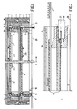
- the system of FIG. 1 is obtained by superposition of three mechanically identical modules 1 so as to form a stack which can include all kinds of functionally different modules.
- the lower module here is different from the other two and has pins 6 for connecting it to a basic printed circuit. As will be seen below, this provision is not mandatory. Side orifices through which pins 21 are accessible allow the connection of a connector 30 to which a sheet of flat conductors 31 is wired.
- a cover 16 covers and protects the assembly. It can be immediately removed to add another module, and replaced on the latter.
- FIG. 2 The components of a module according to the invention are shown in detail in FIG. 2. The manner in which they are assembled will appear further on in the description of FIG. 3.
- the different modules are electrically interconnected with each other to transmit signals.
- the transmission of signals between adjacent modules takes place via metallic wires 7 which protrude outside the module through a slot 14.
- hollow columns 8 are provided as well as screws 9.
- the module of Figure 2 consists of a flat box 1 of insulating material which has the orifice 14 in the form of a slot and a cover 2 also of insulating material.
- the cover is itself assembled to the box by means of hooks 4 which enter the grooves 5.
- the assembly of a stack of such modules is designed to be itself fixed to a printed circuit board called "motherboard" with which contacts can be obtained by means of the same metal wires 7 which come into contact with the areas of the printed circuit board.
- FIG. 2 From the top of FIG. 2 are shown successively a cover 2, an electronic circuit consisting of components 22 wired on a printed flat support 19, then a bar 10 provided with metallic contact wires 7 constituting a plurality of electrical conductors independent of the circuit. To simplify the drawing, four wires have been shown, but it is obvious that the bar is provided over its entire length.
- a box 1 is finally shown. It is here in the form of a frame, and the cover 2 is opened by a wide notch, to allow access to the circuit 19. They could of course also be closed completely.
- the rectangular support 19 is provided with contact pads 28 along its two long sides and to each contact pad on one face of the support corresponds a pad located opposite on the other face. If this support 19 is a printed circuit, the facing pads can be joined by a metallized hole which can be located for example at the edge of these pads. These facing pads can also be electrically connected by jumpers (not shown) placed astride the edge of the substrate, of the type used for the connections of ceramic circuits with thick layers, connections supplied in strips by a number of manufacturers. . This interconnection technique between faces is advantageously used when the support 19 is a ceramic substrate, for example with thick layers.
- the cover 2 is provided with openings 3 through which the areas 28 of the support 19 can be accessed from outside the module, that is to say in FIG. 2, from the top of the cover 2.
- the cover is provided with two four hooks 4 which penetrate into the grooves 5 of the box 1 in order to fix the cover and the box together.
- the box is itself provided with hollow columns 8 intended to hang between them the module shown and a neighboring module to form a stack. Screws 9 penetrate through the columns 8 of the module and the screw of the adjacent module can be screwed into their hollow head.
- the box 1 is provided with slots 14 in which the bar 10 is positioned.
- This strip 10 supports a plurality of electrical conductors 7 constituted by wires elastics of electrically conductive material insulated from each other and held together aligned by the bar.
- the conductors made of elastic wires 7 are each in correspondence with a range of the support 19 and in electrical contact with it. This contact is ensured by a dimensioning of the assembly which causes the wires 7 to be pressed against the pads, located here under the substrate 19, in correspondence with the pads 28 (this arrangement is shown in FIG. 3 which is a section along a plane perpendicular to the bars 10).
- the other end of the wires 7 protrudes outside of the box 1, and can penetrate through the openings 3 of the cover of an adjacent box to come into contact with the areas of a support 19 contained in this adjacent housing.
- the contacts are ensured by means of the conductors 7 between the areas of a circuit placed in a box and those of another circuit placed in another case, a conductor corresponding each time to a range of the support, and the ranges being in from one enclosure to another when the enclosures are attached together.
- connection pins 21 which protrude outside the box and can be connected with a connector plugged into a suitable opening on the side of the box.
- This connector ensures communication only with the corresponding module stage in the stack.
- the bus would be conveyed by the set of vertical connections from one module to another, provided by the metallic wires, and the specific inputs / outputs for each stage would be carried out via pins 21.
- FIG. 3 On both sides of Figure 3, are shown the hooks 4 mentioned above which allow the attachment of the cover 2 and the box 1.
- the bars 10 are shown in section and the figure highlights the manner in which the son 7 come into contact with the jumpers 20 mentioned above, straddling the edges of the ceramic circuits 19 (on the right part of the figure) or else with areas connected together by a metallized hole of a printed circuit (on the part left of the figure).
- a printed circuit will be chosen with a thickness slightly greater than that of the equivalent ceramic support, to compensate for the absence of the jumpers 20 whose thickness is not negligible and arrive at the same total thickness between the contacts opposite.
- the figure also shows how the wires 7 penetrate through the cover of the lower module and are pressed against the jumpers or the pads of the latter's electronic circuit, how they also come (on the left in the figure) in pressure against the motherboard 26 , and how the areas of the upper module circuit are accessible through orifices 3.
- a cover 16 has been shown whose secondary role is to close the upper end of the upper module of the stack to protect the electronic circuit.
- the case shown below and on the right, and its cover, are of a closed model. Below and to the right is shown a particular mode of connection of the circuit 19 to a base plate 26, by means of pins 6 of a known type, fixed to the substrate and which protrude outside the box 1.
- the connection can also be produced, as shown on the left, by the wires 7, supported on the base plate 26.
- a metal plate 27 conductive of heat can be fixed under such a support to evacuate the calories.
- FIG. 4 shows a section along line B of Figure 3. It helps to understand how the radiator 27 protrudes at one end of the support 19, which has no contact pad, to the outside of the housing through an orifice of the housing. This orifice is the same as that through which the above-mentioned connector plugged into the side of the box can be inserted.
- the radiator can be fitted with cooling fins on the outside of the housing. Likewise are shown on the lower stage of the stack of output pins 21, and a connector.30 is suggested in dotted lines.
- FIG. 5 represents a bar element 10 with a conductor 7 made of spring wire. Each wire 7 has two strands wound here on two turns.
- Figure 5b shows in section the bar 10 before mounting a conductor; it has a part 32 in the form of a dovetail which penetrates between the flange and the vertical part of the wire (FIG. 5c) and effectively maintains the latter.
- the modules according to the invention are advantageously used to constitute a microcomputer assembly provided with a microprocessor, its central unit being mounted in one of the modules, a memory in another module, an input / output interface for example to a conversational terminal or to a sensor or a machine actuator being located in a specific module, and in general each functional sub-assembly being constituted by a separate module.
- a microcomputer assembly provided with a microprocessor, its central unit being mounted in one of the modules, a memory in another module, an input / output interface for example to a conversational terminal or to a sensor or a machine actuator being located in a specific module, and in general each functional sub-assembly being constituted by a separate module.
Abstract
Système, par exemple de microinformatique industrielle, constitué par des modules, tous mécaniquement identiques, mais fonctionnellement différents, démontables et reconfigurables. Chaque module comporte un boîtier en deux parties (1, 2), dans lequel est fixé un circuit électronique (19) et qui présente des orifices (3) au travers desquels on peut accéder électriquement au circuit électronique. Il comporte des logements (14) pour fixer une barrette (10) munie de lamelles métalliques (7) qui assurent des contacts avec le circuit électrique et dépassent à l'extérieur du boîtier. Lorsque plusieurs boîtiers sont assemblés, les lamelles (7) qui dépassent à l'extérieur de chaque boîtier sont en contact avec le circuit électronique du boîtier voisin via les orifices (3) de ce dernier.System, for example of industrial microinformatics, constituted by modules, all mechanically identical, but functionally different, removable and reconfigurable. Each module comprises a two-part housing (1, 2), in which an electronic circuit (19) is fixed and which has orifices (3) through which the electronic circuit can be accessed electrically. It comprises housings (14) for fixing a bar (10) provided with metal strips (7) which ensure contacts with the electrical circuit and protrude outside the housing. When several boxes are assembled, the strips (7) which project outside of each box are in contact with the electronic circuit of the neighboring box via the orifices (3) of the latter.
Description
La présente invention concerne un système constitué de modules électroniques attachés les uns aux autres formant ainsi une pile pouvant comporter toutes sortes de modules fonctionnellement différents interconnectés électriquement pour transmettre des signaux entre eux ainsi que vers l'extérieur, ladite pile étant par exemple fixée à une carte de circuit imprimé dite carte mère, chaque module comprenant un circuit électrique constitué de composants câblés sur un support plat imprimé, rectangulaire et muni de plages de contact le long d'au moins un de ses côtés, et placé dans un boitier isolant plat muni de moyens pour maintenir à la fois le circuit et une pluralité de conducteurs électriques indépendants du circuit, un conducteur électriquecorrespondant à chaque fois à une plage du support et étant pressé contre elle, lesdits boitiers étant tous mécaniquement identiques et pourvus de moyens d'accrochage entre eux.The present invention relates to a system consisting of electronic modules attached to each other thus forming a battery which may include all kinds of functionally different modules electrically interconnected to transmit signals between them as well as to the outside, said battery being for example fixed to a printed circuit board known as motherboard, each module comprising an electrical circuit consisting of components wired on a flat printed, rectangular support and provided with contact pads along at least one of its sides, and placed in a flat insulating box provided means for holding both the circuit and a plurality of electrical conductors independent of the circuit, an electrical conductor corresponding each time to a range of the support and being pressed against it, said cases being all mechanically identical and provided with hooking means between them.
De tels modules sont utilisés en électronique lorsque les systèmes doivent être adaptés facilement de façon à satisfaire des besoins spéciaux de l'utilisateur, doivent pouvoir être augmentés en fonction des besoins variables de l'utilisateur et doivent pouvoir être modifiés facilement. Ces modules peuvent donc être rapidement ajoutés à un système ouretirés d'un système, pour modifier ce dernier.Such modules are used in electronics when the systems must be easily adapted to meet special user needs, must be able to be increased according to the varying needs of the user and must be able to be easily modified. These modules can therefore be quickly added to a system or removed from a system, to modify the latter.
Un tel système est décrit dans un article du 1er janvier 1985 de la revue "Electronics week" pages 97, 98, intitulé "Domino-like modules build computers", et représenté par la photographie qui accompagne cet article. Un système du même genre est décrit plus en détails par le brevet US-A-4045105.Such a system is described in an article of January 1, 1985 of the review "Electronics week" pages 97, 98, entitled "Domino-like modules build computers", and represented by the photograph which accompanies this article. A system of the same kind is described in more detail by patent US-A-4045105.
Ces systèmes sont basés sur l'emploi de broches et de douilles complexes et relativement coûteuses. En outre, ces broches introduisent des contacts intermédiaires entre deux circuits voisins, ce qui augmente la résistance des connexions et diminue la fiabilité.These systems are based on the use of complex and relatively expensive pins and sockets. In addition, these pins introduce intermediate contacts between two neighboring circuits, which increases the resistance of the connections and reduces reliability.
L'invention se propose de fournir un mode °- tion d'un tel système dans lequel on utilise des circuits tels que des circuits imprimés ou des substrats dits hybrides à couches épaisses ou à couches minces, sur lesquels la totalité des composants utilisés peuvent être montés en une seule passe selon une technologie standard.The invention proposes to provide a mode ° - tion of such a system in which circuits are used such as printed circuits or so-called hybrid substrates with thick layers or thin layers, on which all of the components used can be mounted in a single pass according to standard technology.
L'invention fournit des boîtiers spécialement adaptés à la tenue mécanique des circuits et à leur interconnexion et qui autorisent le maximum d'interchangeabilité, de densité, de modularité, et permettent une grande souplesse en ce qui concerne les entrées/sorties spécifiques de chaque circuit et la puissance qu'ils peuvent dissiper. Elle permet en outre d'obtenir des connexions entre substrats voisins qui, tout en restant immédiatement démontables, ont une excellente résistance électrique et une excellente fiabilité.The invention provides boxes specially adapted to the mechanical strength of the circuits and their interconnection and which allow maximum interchangeability, density, modularity, and allow great flexibility with regard to the specific inputs / outputs of each circuit. and the power they can dissipate. It also makes it possible to obtain connections between neighboring substrates which, while remaining immediately removable, have excellent electrical resistance and excellent reliability.
Le système selon l'invention est notamment remarquable en ce que ledit support étant rectangulaire et muni de plages de contact le long d'au moins un de ses cotés, à chaque plage de contact sur une face du support correspond une plage située en vis à vis sur l'autre face et qui lui est électriquement reliée, en ce que le boitier laisse dépasser au travers d'une seule face lesdits conducteurs électriques et est muni d'ouvertures situées sur l'autre face, qui laissent apparaitre certaines plages du support, et en ce que, au moyen desdits conducteurs dont l'extrémité est élastique, des contacts sont assurés entre les plages d'un circuit placé dans un boitier et celles d'un autre circuit placé dans un autre boitier, plages qui sont elles-même en vis à vis lorsque les boitiers sont attachés.The system according to the invention is notably remarkable in that said support being rectangular and provided with contact pads along at least one of its sides, to each contact pad on one face of the support corresponds a pad located opposite screw on the other side and which is electrically connected to it, in that the casing allows said electrical conductors to protrude through a single side and is provided with openings located on the other side, which reveal certain areas of the support , and in that, by means of said conductors, the end of which is elastic, contacts are ensured between the areas of a circuit placed in a case and those of another circuit placed in another case, areas which are themselves- even opposite when the boxes are attached.
Ladite pluralité de conducteurs électriques est avantageusement constituée par des fils élastiques en matériau électriquement conducteur isolés les uns des autres et tenus ensemble alignés par une barrette isolante, le boîtier comportant un logement pour maintenir en position ladite barrette isolante avec ses conducteurs. Ces fils élastiques sontavantageusement faits en fil à ressort et comportent des boudinsenroulés chacun sur au moins un tour. En outre les barrettes isolantes présentent, entre les deux boudins de chaque conducteurs, une partie en forme de queue d'aronde pour maintenir le conducteur.Said plurality of electrical conductors is advantageously constituted by elastic wires of electrically conductive material insulated from each other and held together aligned by an insulating strip, the housing comprising a housing for holding said insulating strip in position with its conductors. These elastic threads are advantageously made of spring wire and comprise rolls each wound over at least one revolution. In addition the insulating bars have, between the two strands of each conductor, a part in the form of a dovetail to hold the conductor.
Selon un mode de réalisation particulier où au moins un circuit est muni d'une plaque-radiateur, cette plaque dépasse à l'extérieur du circuit d'un côté qui ne comporte pas de plages de contact, et les boîtiers sont munis d'un orifice en correspondance avec cette plaque pour la laisser dépasser à l'extérieur.According to a particular embodiment where at least one circuit is provided with a radiator plate, this plate protrudes outside the circuit on one side which does not have contact pads, and the housings are provided with a orifice in correspondence with this plate to let it protrude outside.
Selon un autre mode de réalisation particulier où au moins un circuit émet ou reçoit certains signaux exclusivement vers l'extérieur, ou de l'extérieur, le support comporte des connexions le long d'un côté qui ne sert ni au refroidissement ni au contact vers les autres modules via les susdits conducteurs, et les boîtiers comportent une ouverture en correspondance avec ce côté pour permettre l'introduction d'un connecteur.According to another particular embodiment where at least one circuit transmits or receives certain signals exclusively to the outside, or from the outside, the support has connections along one side which is neither used for cooling nor for contact to the other modules via the above conductors, and the boxes have an opening corresponding to this side to allow the introduction of a connector.
L'invention concerne en particulier un système à usage industriel muni d'un micro-processeur, remarquable en ce que son unité centrale, ses modules de mémoire, ses interfaces de liaison entrée/sortie sont constitués chacun par un module selon l'invention.The invention relates in particular to a system for industrial use provided with a microprocessor, remarkable in that its central unit, its memory modules, its input / output link interfaces each consist of a module according to the invention.
La description qui va suivre en regard des dessins annexés décrivant des exemples non limitatifs fera bien comprendrecomment l'invention peut être réalisée.The description which follows with reference to the appended drawings describing nonlimiting examples will make it clear how the invention can be made.
- La figure 1 représente vu en perspective, un système électronique selon l'invention.Figure 1 shows a perspective view of an electronic system according to the invention.
- La figure 2 représente une vue éclatée d'un module élémentaire du système.FIG. 2 represents an exploded view of an elementary module of the system.
- La figure 3 représente une vue en coupe d'un empilage de deux modules et la figure 4 représente une autre vue en coupedu même empilage de modules.Figure 3 shows a sectional view of a stack of two modules and Figure 4 shows another sectional view of the same stack of modules.
-
La figure 5 représente à plus grande échelle une partie de la barrette 10 et un conducteur 7 de la figure 2.FIG. 5 represents on a larger scale part of the
strip 10 and aconductor 7 of FIG. 2.
Le système de la figure 1 est obtenu par superposition de trois modules 1 mécaniquement identiques de manière à former une pile pouvant comporter toutes sortes de modules fonctionnellement différents. Le module inférieur est ici différent des deux autres et comporte des broches 6 pour le relier à un circuit imprimé de base. Comme on le verra plus loin, cette disposition n'est pas obligatoire. Des orifices latéraux au travers desquels sont accessibles des broches 21 permettent le branchement d'un connecteur 30 auquel une nappe deconducteurs plats 31 est cablée. Un couvercle 16 recouvre et protège l'ensemble. Il peut être immédiatement enlevé pour ajouter un autre module, et replacé sur ce dernier.The system of FIG. 1 is obtained by superposition of three mechanically
Les constituants d'un module selon l'invention sont représentés en détail sur la figure 2. La manière dont ils s'assemblent apparaitra plus loin lors de la description de la figure 3.The components of a module according to the invention are shown in detail in FIG. 2. The manner in which they are assembled will appear further on in the description of FIG. 3.
Les différents modules sont interconnectés électriquement entre eux pour transmettre des signaux. La transmission des signaux entre modules adjacents se fait par l'intermédiaire de fils métalliques 7 qui dépassent à l'extérieur du module au travers d'une fente 14. Pour accrocher les modules les uns aux autres, des colonnes creuses 8 sont prévues ainsi que des vis 9. Le module de la figure 2 est constitué par une boîte plate 1 en matériau isolant qui comporte l'orifice 14 en forme de fente et un couvercle 2 également en matériau isolant.The different modules are electrically interconnected with each other to transmit signals. The transmission of signals between adjacent modules takes place via
Le couvercle est lui-même assemblé à la boite au moyende crochets 4 qui entrent dans les gorges 5. L'ensemble d'un empilage de tels modules est conçu pour être lui-même fixé à uneplaque de circuit imprimé dite "carte mère" avec laquelle des contacts peuvent être obtenus au moyen des mêmes fils métalliques 7 qui entrent en contact avec les plages de la cartemère de circuit imprimé.The cover is itself assembled to the box by means of hooks 4 which enter the
A partir du haut de la figure 2 sont représentés successivement un couvercle 2, un circuit électronique constituéde composants 22 câblés sur un support plat imprimé 19, puis une barette 10 munie de fils métallique de contact 7 constituant une pluralité de conducteurs électriques indépendants du circuit. Pour simplifier le dessin, quatre fils ont été représentés mais il est bien évident que la barrette en est pourvue sur toute sa longueur. Une boite 1 est enfin représentée. Elle est ici en forme de cadre, et le couvercle 2 est ouvert par une large échancrure, pour permettre un accès vers le circuit 19. Ils pourraient bien entendu aussi être fermés complètement.From the top of FIG. 2 are shown successively a
Le support 19 rectangulaire est muni de plages de contact 28 le long de ses deux grands côtés et à chaque plage de contact sur une face du support correspond une plage située en vis à vis sur l'autre face. Si ce support 19 est un circuit imprimé, les plages en vis à vis peuvent être réunies par un trou métallisé qui peut être situé par exemple en bordure de ces plages. Ces plages en vis à vis peuvent aussi être électriquement reliées par des cavaliers (non représentés) placés à cheval sur la tranche du substrat, du type employé pour les connexions des circuits céramiques à couches épaisses, connexions fournies en bande par un certain nombre de fabricants. Cette technique d'interconnexion entre faces est employée avantageusement lorsque le support 19 est un substrat de céramique par exemple à couches épaisses.The
Le couvercle 2 est muni d'ouvertures 3 au travers desquelles les plages 28 du support 19 peuvent être accessibles à partir de l'extérieur du module c'est-à-dire, sur la figure 2, à partir du dessus du couvercle 2. Le couvercle est muni de deux fois quatre crochets 4 qui pénétrent dans les gorges 5 de la boîte 1 afin de fixer ensemble le couvercle et la boîte. La boîte est elle même munie des colonnes creuses 8 destinées à accrocher entre eux le module représenté et un .module voisin pour former un empilage. Des vis 9 pénètrent au travers des colonnes 8 du module et dans leur tête creuse peut être vissée la vis du module ajacent.The
La boîte 1 est munie de fentes 14 dans lesquelles la barrette 10 est positionnée. Cette barrette 10 supporte une pluralité de conducteurs électriques 7 constitués par des fils élastiques en matériau électriquement conducteur isolés les uns des autres et tenus ensemble alignés par la barrette. Lorsque la barrette 10 est montée dans la fente 14 et que le support 19 est monté dans la boite 1, et fixé au moyen des tétons 15 entrant dans des trous 13 et par exemple écrasés à chaud, les conducteurs constitués de fils élastiques 7 sont chacun en correspondance avec une plage du support 19 et en contact électrique avec elle. Ce contact est assuré par un dimensionnement de l'ensemble qui amène les fils 7 à être pressés contre les plages, situées ici sous le substrat 19, en correspondance avec les plages 28 (cette disposition est montrée sur la figure 3 qui est une coupe selon un plan perpendiculaire aux barrettes 10). L'autre extrémité des fils 7 (par rapport à celle qui est pressée contre les plages) dépasse à l'extérieur de la boite 1, et peut pénétrer au travers des ouvertures 3 du couvercle d'un boîtier adjacent pour venir en contact avec les plages d'un support 19 contenu dans ce boîtier adjacent. Ainsi les contacts sont assurés au moyen des conducteurs 7 entre les plages d'un circuit placé dans un boitier et celles d'un autre circuit placé dans un autre boîtier, un conducteur correspondant chaque fois à une plage du support, et les plages étant en vis à vis d'un boîtier à l'autre lorsque les boîtiers sont attachés ensemble.The
Un côté du support 19 qui ne porte pas les plages 28 destinées à l'interconnexion des modules entre eux peut être utilisé pour y placer des broches de connexion 21 qui dépassent à l'extérieur de la boîte et peuvent être mises en connexion avec un connecteur enfiché dans une ouverture appropriée sur le côté de la boîte. Ce connecteur assure une communication seulement avec l'étage de module correspondant dans l'empilage. Par exemple dans un système informatique le bus serait véhiculé par l'ensemble de connexions verticales d'un module à l'autre, assurées par les fils métalliques, et les entrées/sorties spécifiques à chaque étage seraient effectuées via les broches 21.One side of the
Des deux cotés de la figure 3, sont représentés les crochets 4 mentionnés plus haut qui permettent l'accrochage du couvercle 2 et de la boîte 1. Les barrettes 10 sont représentées en coupe et la figure met en évidence la manière selon laquelle les fils 7 entrent en contact avec les cavaliers 20 mentionnés plus haut, à cheval sur les bords des circuits céramique 19 (sur la partie droite de la figure ) ou bien avec des plages reliées entre elles par un trou métallisé d'un circuit imprimé (sur la partie gauche de la figure). Un circuit imprimé sera choisi avec une épaisseur légèrement plus grande que celle du support céramique équivalent, pour compenser l'absence des cavaliers 20 dont l'épaisseur n'est pas négligeable et arriver à la même épaisseur totale entre les contacts en vis à vis. La figure montre également comment les fils 7 pénètrent au travers du couvercle du module inférieur et sont pressés contre les cavaliers ou les plages du circuit électronique de ce dernier, comment elles viennent également (à gauche sur la figure) en pression contre la carte mère 26, et comment les plages du circuit du module supérieur sont accessibles au travers d'orifices 3. Un couvercle 16 a été représenté dont le rôle secondaire est de fermer l'extrémité supérieure du module supérieur de l'empilage pour en protéger le circuit électronique. Le boitier représenté en bas et à droite, et son couvercle, sont d'un modèle fermé. En bas et à droite on a représenté un mode particulier de connexion du circuit 19 à une plaque de base 26, au moyen de broches 6 d'un type connu, fixées au substrat et qui dépassent à l'extérieur dela boite 1. La connexion peut aussi être réalisée, comme représenté à gauche, par les fils 7, appuyés sur la plaque de base 26.On both sides of Figure 3, are shown the hooks 4 mentioned above which allow the attachment of the
Fixés aux supports de circuit électronique sont représentés des composants 22a, b, c pour suggérer diverses possibilités de montage sur lesdits supports. En outre une plaque métallique 27 conductrice de la chaleur peut être fixée sous un tel support pour en évacuer les calories.Fixed to the electronic circuit supports are shown
La figure 4 représente une coupe selon la ligne B de la figure 3. Elle permet de bien comprendre comment le radiateur 27 dépasse à une extrémité du support 19, qui ne comporte pas de plage de contact, jusqu'à l'extérieur du boîtier en passant par un orifice du boîtier. Cet orifice est le même que celui par lequel on peut introduire le susdit connecteur enfiché sur le côté de la boite. Le radiateur peut être muni d'ailettes de refroidissement à l'extérieur du boîtier. De même sont représentées à l'étage inférieur de l'empilement des broches de sortie 21, et un connecteur.30 est suggéré en pointillés. La figure 5 représente un élément de barrette 10 avec un conducteur 7 fait en fil à ressort. Chaque fil 7 comporte deux boudins enroulés ici sur deux tours. Ces fils boudinés autorisent une grande amplitude de déplacement élastique de l'extrémité du fil et permettent d'assurer un excellent contact, même avec de larges tolérances mécaniques. La figure 5b montre en coupe la barrette 10 avant le montage d'un conducteur ; elle présente une partie 32 en forme de queue d'aronde qui pénètre entre le boudin et la partie verticale du fil (figure 5c) et maintient efficacement ce dernier.Figure 4 shows a section along line B of Figure 3. It helps to understand how the
Les modules selon l'invention sont utilisés avantageusement pour constituer un ensemble de micro-informatique muni d'un microprocesseur, son unité centrale étant montée dans un des modules, une mémoire dans un autre module, une interface d'entrée/sortie par exemple vers un terminal conversationnel ou vers un capteur ou un actionneur de machine étant située dans unmodule spécifique, et d'une manière générale chaque sous-ensemble fonctionnel étant constitué par un module distinct. Ainsi toute configuration peut être constituée à la demande et reconfigurée très facilement en assemblant des modules selon l'invention.The modules according to the invention are advantageously used to constitute a microcomputer assembly provided with a microprocessor, its central unit being mounted in one of the modules, a memory in another module, an input / output interface for example to a conversational terminal or to a sensor or a machine actuator being located in a specific module, and in general each functional sub-assembly being constituted by a separate module. Thus any configuration can be constituted on demand and reconfigured very easily by assembling modules according to the invention.
Claims (8)
Applications Claiming Priority (2)
| Application Number | Priority Date | Filing Date | Title |
|---|---|---|---|
| FR8505263A FR2580136B1 (en) | 1985-04-05 | 1985-04-05 | |
| FR8505263 | 1985-04-05 |
Publications (2)
| Publication Number | Publication Date |
|---|---|
| EP0196726A1 true EP0196726A1 (en) | 1986-10-08 |
| EP0196726B1 EP0196726B1 (en) | 1990-07-04 |
Family
ID=9318024
Family Applications (1)
| Application Number | Title | Priority Date | Filing Date |
|---|---|---|---|
| EP86200537A Expired - Lifetime EP0196726B1 (en) | 1985-04-05 | 1986-04-01 | Electronic system consisting of stacking modules |
Country Status (5)
| Country | Link |
|---|---|
| US (1) | US4688864A (en) |
| EP (1) | EP0196726B1 (en) |
| JP (1) | JPS61234598A (en) |
| DE (1) | DE3672362D1 (en) |
| FR (1) | FR2580136B1 (en) |
Cited By (3)
| Publication number | Priority date | Publication date | Assignee | Title |
|---|---|---|---|---|
| WO1987006092A1 (en) * | 1986-03-25 | 1987-10-08 | Dowty Electronic Components Limited | Interconnection systems for electrical circuits |
| EP0361821A2 (en) * | 1988-09-30 | 1990-04-04 | THOMAS & BETTS CORPORATION | Electrical connector for module packaging |
| US5113316A (en) * | 1989-11-07 | 1992-05-12 | Marelli Autronica Spa | System for the assembly and connection of electronic circuit boards, particularly for use in motor vehicles |
Families Citing this family (56)
| Publication number | Priority date | Publication date | Assignee | Title |
|---|---|---|---|---|
| US5013249A (en) * | 1986-06-19 | 1991-05-07 | Labinal Components And Systems, Inc. | Electrical connectors |
| US5597313A (en) * | 1986-06-19 | 1997-01-28 | Labinal Components And Systems, Inc. | Electrical connectors |
| US5672062A (en) * | 1991-01-30 | 1997-09-30 | Labinal Components And Systems, Inc. | Electrical connectors |
| EP0265698B1 (en) * | 1986-09-30 | 1994-03-30 | Fauzi Bekhiet | Connection device for the electrical connection of the connection points of electrical apparatuses |
| JP2565535B2 (en) * | 1988-02-29 | 1996-12-18 | 日本電気ホームエレクトロニクス株式会社 | Processor module |
| JPH0750863Y2 (en) * | 1988-06-13 | 1995-11-15 | キヤノン株式会社 | Small DC motor |
| US4966562A (en) * | 1988-09-06 | 1990-10-30 | The Ohio Bell Telephone Company | Single slot repeater mounting |
| US4867689A (en) * | 1988-10-31 | 1989-09-19 | Amp Incorporated | Elastomeric connector assembly |
| GR880100760A (en) * | 1988-11-10 | 1990-12-31 | Telefonica Nacional Espana Co | Flexible interconnection system of electronic equipment |
| US5056151A (en) * | 1989-09-19 | 1991-10-08 | Gennum Corporation | Electrical component connection and combinations of electrical components |
| ES2142803T3 (en) * | 1990-08-01 | 2000-05-01 | Diomed Ltd | HIGH POWER LIGHT SOURCE. |
| US5124886A (en) * | 1991-02-25 | 1992-06-23 | Ncr Corporation | Drive canister mounting module |
| US5169320A (en) * | 1991-09-27 | 1992-12-08 | Hercules Defense Electronics Systems, Inc. | Shielded and wireless connector for electronics |
| US5137456A (en) * | 1991-11-04 | 1992-08-11 | International Business Machines Corporation | High density, separable connector and contact for use therein |
| US5181852A (en) * | 1991-12-16 | 1993-01-26 | Molex Incorporated | Programmable input-output electrical connector |
| EP0581471A1 (en) * | 1992-07-29 | 1994-02-02 | Fujitsu Limited | Image control apparatus |
| US6205654B1 (en) | 1992-12-11 | 2001-03-27 | Staktek Group L.P. | Method of manufacturing a surface mount package |
| US5383787A (en) * | 1993-04-27 | 1995-01-24 | Aptix Corporation | Integrated circuit package with direct access to internal signals |
| US5868678A (en) * | 1993-06-30 | 1999-02-09 | Medex, Inc. | Two-part medical pressure transducer with diaphragm stand-offs |
| US5752918A (en) * | 1993-06-30 | 1998-05-19 | Medex, Inc. | Modular medical pressure transducer |
| US5417395A (en) * | 1993-06-30 | 1995-05-23 | Medex, Inc. | Modular interconnecting component support plate |
| US5497027A (en) * | 1993-11-30 | 1996-03-05 | At&T Global Information Solutions Company | Multi-chip module packaging system |
| US5564932A (en) * | 1994-11-14 | 1996-10-15 | Castleman; Mark-Andrew B. | Customizeable interconnect device for stacking electrical components of varying configuration |
| US5677830A (en) * | 1995-03-02 | 1997-10-14 | Mitel Corporation | Modular, stacking, expandable electronic enclosure system |
| US5514907A (en) * | 1995-03-21 | 1996-05-07 | Simple Technology Incorporated | Apparatus for stacking semiconductor chips |
| US5829723A (en) * | 1995-06-28 | 1998-11-03 | Medex, Inc. | Medical device mounting structure |
| US5564802A (en) * | 1995-09-14 | 1996-10-15 | Chiou; Ming D. | Diskdrive case |
| JPH0982431A (en) * | 1995-09-19 | 1997-03-28 | Whitaker Corp:The | Electric connector and its preparation |
| US5841639A (en) * | 1995-10-26 | 1998-11-24 | The Whitaker Corporation | Expansion module for a communcations network |
| US5825618A (en) * | 1995-10-26 | 1998-10-20 | The Whitaker Corporation | Hub for a communications network |
| US5838548A (en) * | 1995-10-26 | 1998-11-17 | The Whitaker Corporation | Network apparatus |
| US5761459A (en) * | 1995-10-26 | 1998-06-02 | The Whitaker Corporation | Mechanism for a communications network |
| KR970049283A (en) * | 1995-12-28 | 1997-07-29 | 김광호 | Easy to expand computer |
| US6295220B1 (en) | 1998-11-03 | 2001-09-25 | Zomaya Group, Inc. | Memory bar and related circuits and methods |
| US6190425B1 (en) | 1998-11-03 | 2001-02-20 | Zomaya Group, Inc. | Memory bar and related circuits and methods |
| US6560102B1 (en) * | 2000-10-23 | 2003-05-06 | Belkin Components | Universal serial bus docking station |
| CA2319296A1 (en) * | 1999-09-17 | 2001-03-17 | Thomas & Betts International, Inc. | Stacked smart card reader assembly |
| US6572387B2 (en) | 1999-09-24 | 2003-06-03 | Staktek Group, L.P. | Flexible circuit connector for stacked chip module |
| US6608763B1 (en) | 2000-09-15 | 2003-08-19 | Staktek Group L.P. | Stacking system and method |
| US6462408B1 (en) | 2001-03-27 | 2002-10-08 | Staktek Group, L.P. | Contact member stacking system and method |
| US20060190106A1 (en) | 2001-07-30 | 2006-08-24 | Rockwell Automation Technologies, Inc. | Method for consistent storage of data in an industrial controller |
| US7167372B2 (en) * | 2003-08-26 | 2007-01-23 | Belkin Corporation | Universal serial bus hub and method of manufacturing same |
| US7088972B2 (en) * | 2002-10-15 | 2006-08-08 | Honeywell Federal Manufacturing & Technologies, Llp | Distributed data transmitter |
| US8014170B2 (en) | 2003-08-26 | 2011-09-06 | Belkin International, Inc. | Cable management device and method of cable management |
| US7329152B2 (en) * | 2003-08-26 | 2008-02-12 | Belkin International, Inc. | Universal serial bus hub and method of manufacturing same |
| US7273378B2 (en) * | 2003-09-19 | 2007-09-25 | Mitsumi Electric Co., Ltd. | Connecting device |
| US7116553B2 (en) * | 2003-11-07 | 2006-10-03 | Scimeasure Analytical Systems, Inc. | Circuit board enclosure |
| US7806723B2 (en) * | 2007-01-05 | 2010-10-05 | Belkin International, Inc. | Electrical grommet device |
| US20060258195A1 (en) * | 2005-05-11 | 2006-11-16 | Ameriwood Industries, Inc. | Connectivity system, method of assembling same, and desk containing same |
| US7381095B2 (en) * | 2005-06-20 | 2008-06-03 | Belkin International, Inc. | Multi-standard connection hub and method of manufacturing same |
| US7660112B2 (en) * | 2007-05-08 | 2010-02-09 | Dell Products L.P. | Component bay |
| US20100319986A1 (en) * | 2009-06-17 | 2010-12-23 | Bleau Charles A | Modular vented circuit board enclosure |
| DE102009054639A1 (en) * | 2009-12-15 | 2011-06-16 | Robert Bosch Gmbh | Hand tool add-on module |
| TW201318284A (en) * | 2011-10-21 | 2013-05-01 | Acer Inc | Male connector and female connector in computer system |
| JP6458745B2 (en) * | 2016-02-18 | 2019-01-30 | オムロン株式会社 | Device unit |
| JP6589028B1 (en) * | 2018-09-21 | 2019-10-09 | 有限会社アイ電気 | Electronic circuit holder |
Citations (8)
| Publication number | Priority date | Publication date | Assignee | Title |
|---|---|---|---|---|
| US3551750A (en) * | 1969-04-21 | 1970-12-29 | Hugh H Eby Co | Circuit board connector |
| DE2037385A1 (en) * | 1970-07-28 | 1972-02-03 | North American Rockwell | Electronic assembly |
| FR2096541A1 (en) * | 1970-06-29 | 1972-02-18 | Ibm | |
| US3904934A (en) * | 1973-03-26 | 1975-09-09 | Massachusetts Inst Technology | Interconnection of planar electronic structures |
| US4045105A (en) * | 1974-09-23 | 1977-08-30 | Advanced Memory Systems, Inc. | Interconnected leadless package receptacle |
| GB2095039A (en) * | 1981-02-10 | 1982-09-22 | Brown David F | Circuit assembly |
| US4395084A (en) * | 1981-07-06 | 1983-07-26 | Teledyne Industries, Inc. | Electrical socket for leadless integrated circuit packages |
| GB2130025A (en) * | 1982-11-08 | 1984-05-23 | Control Data Corp | Memory board stacking module |
Family Cites Families (3)
| Publication number | Priority date | Publication date | Assignee | Title |
|---|---|---|---|---|
| US3454921A (en) * | 1965-10-23 | 1969-07-08 | Westinghouse Electric Corp | Electronic component carrier |
| GB1343451A (en) * | 1971-03-12 | 1974-01-10 | Plessey Co Ltd | Electrical connectors |
| US4437718A (en) * | 1981-12-17 | 1984-03-20 | Motorola Inc. | Non-hermetically sealed stackable chip carrier package |
-
1985
- 1985-04-05 FR FR8505263A patent/FR2580136B1/fr not_active Expired
-
1986
- 1986-03-28 US US06/845,653 patent/US4688864A/en not_active Expired - Fee Related
- 1986-04-01 EP EP86200537A patent/EP0196726B1/en not_active Expired - Lifetime
- 1986-04-01 DE DE8686200537T patent/DE3672362D1/en not_active Expired - Lifetime
- 1986-04-05 JP JP61077572A patent/JPS61234598A/en active Pending
Patent Citations (8)
| Publication number | Priority date | Publication date | Assignee | Title |
|---|---|---|---|---|
| US3551750A (en) * | 1969-04-21 | 1970-12-29 | Hugh H Eby Co | Circuit board connector |
| FR2096541A1 (en) * | 1970-06-29 | 1972-02-18 | Ibm | |
| DE2037385A1 (en) * | 1970-07-28 | 1972-02-03 | North American Rockwell | Electronic assembly |
| US3904934A (en) * | 1973-03-26 | 1975-09-09 | Massachusetts Inst Technology | Interconnection of planar electronic structures |
| US4045105A (en) * | 1974-09-23 | 1977-08-30 | Advanced Memory Systems, Inc. | Interconnected leadless package receptacle |
| GB2095039A (en) * | 1981-02-10 | 1982-09-22 | Brown David F | Circuit assembly |
| US4395084A (en) * | 1981-07-06 | 1983-07-26 | Teledyne Industries, Inc. | Electrical socket for leadless integrated circuit packages |
| GB2130025A (en) * | 1982-11-08 | 1984-05-23 | Control Data Corp | Memory board stacking module |
Cited By (5)
| Publication number | Priority date | Publication date | Assignee | Title |
|---|---|---|---|---|
| WO1987006092A1 (en) * | 1986-03-25 | 1987-10-08 | Dowty Electronic Components Limited | Interconnection systems for electrical circuits |
| US4872843A (en) * | 1986-03-25 | 1989-10-10 | Dowty Electronic Components Limited | Interconnection systems for electrical circuits |
| EP0361821A2 (en) * | 1988-09-30 | 1990-04-04 | THOMAS & BETTS CORPORATION | Electrical connector for module packaging |
| EP0361821A3 (en) * | 1988-09-30 | 1990-10-24 | THOMAS & BETTS CORPORATION | Electrical connector for module packaging |
| US5113316A (en) * | 1989-11-07 | 1992-05-12 | Marelli Autronica Spa | System for the assembly and connection of electronic circuit boards, particularly for use in motor vehicles |
Also Published As
| Publication number | Publication date |
|---|---|
| US4688864A (en) | 1987-08-25 |
| FR2580136A1 (en) | 1986-10-10 |
| EP0196726B1 (en) | 1990-07-04 |
| DE3672362D1 (en) | 1990-08-09 |
| JPS61234598A (en) | 1986-10-18 |
| FR2580136B1 (en) | 1988-10-14 |
Similar Documents
| Publication | Publication Date | Title |
|---|---|---|
| EP0196726B1 (en) | Electronic system consisting of stacking modules | |
| FR2792803A1 (en) | CARD-MOUNTED SEMICONDUCTOR DEVICE | |
| US5434747A (en) | Photoelectric transducer | |
| EP1114574B1 (en) | Connecting device for an assembly of line replaceable modules for electronic wallets and rack equipped with same for receiving such an assembly | |
| EP0170543B1 (en) | Mechanical and electrical assembling device for highly integrated electronic computer circuit boards | |
| US4571663A (en) | Electrical circuit assemblies | |
| US4107760A (en) | Dual printed circuit card mount assembly | |
| US20080305692A1 (en) | Electrical connector assembly | |
| RU2602074C2 (en) | Connector | |
| FR2773301A1 (en) | ADAPTABLE PLAN MODULE FOR HOUSING SEMICONDUCTOR DEVICES | |
| FR2878118A1 (en) | CIRCUIT MODULE, METHOD FOR ASSEMBLING THE SAME, SYSTEM FOR EXTRACTING HEAT ENERGY FROM CIRCUIT MODULE, AND THERMAL MANAGEMENT SYSTEM | |
| EP0233674A1 (en) | Information bus connector | |
| FR2529429A1 (en) | GROUP OF ELECTRICAL APPLIANCES MOUNTED ON A COMMON SUPPORT PROFILE | |
| JP4126240B2 (en) | Circuit board assembly structure | |
| CN1112354A (en) | Junction box and PCB assembly therefor | |
| US6088227A (en) | Heat sink with integrated buss bar | |
| EP1550361B1 (en) | Three-dimensional electronic module | |
| KR101821420B1 (en) | Socket | |
| US3313986A (en) | Interconnecting miniature circuit modules | |
| FR2855710A1 (en) | Control apparatus for motor vehicle, has spacer blocked between printed circuit boards to electrically connect boards, and connection pins of electronic components contacting with one board based on spacer arrangement | |
| JPS5816311B2 (en) | Komid Connector Plug Assembly | |
| NL8701350A (en) | SWITCHING DEVICE FOR CONNECTION TO CONTACTS IN A ROW. | |
| EP0346206A1 (en) | Active connector for printed-circuit boards | |
| EP0603026B1 (en) | Protection device for electronic installations against transients generated by phenomena affecting the environment outside of the installation | |
| US5924876A (en) | High density electrical connector having an alignment feature |
Legal Events
| Date | Code | Title | Description |
|---|---|---|---|
| PUAI | Public reference made under article 153(3) epc to a published international application that has entered the european phase |
Free format text: ORIGINAL CODE: 0009012 |
|
| AK | Designated contracting states |
Kind code of ref document: A1 Designated state(s): DE FR GB NL |
|
| 17P | Request for examination filed |
Effective date: 19870316 |
|
| 17Q | First examination report despatched |
Effective date: 19880906 |
|
| GRAA | (expected) grant |
Free format text: ORIGINAL CODE: 0009210 |
|
| RAP1 | Party data changed (applicant data changed or rights of an application transferred) |
Owner name: N.V. PHILIPS' GLOEILAMPENFABRIEKEN Owner name: PHILIPS COMPOSANTS |
|
| AK | Designated contracting states |
Kind code of ref document: B1 Designated state(s): DE FR GB NL |
|
| PG25 | Lapsed in a contracting state [announced via postgrant information from national office to epo] |
Ref country code: NL Effective date: 19900704 |
|
| REF | Corresponds to: |
Ref document number: 3672362 Country of ref document: DE Date of ref document: 19900809 |
|
| GBT | Gb: translation of ep patent filed (gb section 77(6)(a)/1977) | ||
| NLV1 | Nl: lapsed or annulled due to failure to fulfill the requirements of art. 29p and 29m of the patents act | ||
| PG25 | Lapsed in a contracting state [announced via postgrant information from national office to epo] |
Ref country code: GB Effective date: 19910401 |
|
| PLBE | No opposition filed within time limit |
Free format text: ORIGINAL CODE: 0009261 |
|
| STAA | Information on the status of an ep patent application or granted ep patent |
Free format text: STATUS: NO OPPOSITION FILED WITHIN TIME LIMIT |
|
| 26N | No opposition filed | ||
| GBPC | Gb: european patent ceased through non-payment of renewal fee | ||
| PG25 | Lapsed in a contracting state [announced via postgrant information from national office to epo] |
Ref country code: FR Effective date: 19911230 |
|
| PG25 | Lapsed in a contracting state [announced via postgrant information from national office to epo] |
Ref country code: DE Effective date: 19920201 |
|
| REG | Reference to a national code |
Ref country code: FR Ref legal event code: ST |