EP0197438A1 - Method of manufacturing electronic modules for microcircuit boards and modules obtained by this method - Google Patents
Method of manufacturing electronic modules for microcircuit boards and modules obtained by this method Download PDFInfo
- Publication number
- EP0197438A1 EP0197438A1 EP86104178A EP86104178A EP0197438A1 EP 0197438 A1 EP0197438 A1 EP 0197438A1 EP 86104178 A EP86104178 A EP 86104178A EP 86104178 A EP86104178 A EP 86104178A EP 0197438 A1 EP0197438 A1 EP 0197438A1
- Authority
- EP
- European Patent Office
- Prior art keywords
- chip
- recess
- grid
- windows
- tabs
- Prior art date
- Legal status (The legal status is an assumption and is not a legal conclusion. Google has not performed a legal analysis and makes no representation as to the accuracy of the status listed.)
- Granted
Links
Images


Classifications
-
- G—PHYSICS
- G06—COMPUTING; CALCULATING OR COUNTING
- G06K—GRAPHICAL DATA READING; PRESENTATION OF DATA; RECORD CARRIERS; HANDLING RECORD CARRIERS
- G06K19/00—Record carriers for use with machines and with at least a part designed to carry digital markings
- G06K19/06—Record carriers for use with machines and with at least a part designed to carry digital markings characterised by the kind of the digital marking, e.g. shape, nature, code
- G06K19/067—Record carriers with conductive marks, printed circuits or semiconductor circuit elements, e.g. credit or identity cards also with resonating or responding marks without active components
- G06K19/07—Record carriers with conductive marks, printed circuits or semiconductor circuit elements, e.g. credit or identity cards also with resonating or responding marks without active components with integrated circuit chips
- G06K19/077—Constructional details, e.g. mounting of circuits in the carrier
- G06K19/07745—Mounting details of integrated circuit chips
- G06K19/07747—Mounting details of integrated circuit chips at least one of the integrated circuit chips being mounted as a module
-
- G—PHYSICS
- G06—COMPUTING; CALCULATING OR COUNTING
- G06K—GRAPHICAL DATA READING; PRESENTATION OF DATA; RECORD CARRIERS; HANDLING RECORD CARRIERS
- G06K19/00—Record carriers for use with machines and with at least a part designed to carry digital markings
- G06K19/06—Record carriers for use with machines and with at least a part designed to carry digital markings characterised by the kind of the digital marking, e.g. shape, nature, code
- G06K19/067—Record carriers with conductive marks, printed circuits or semiconductor circuit elements, e.g. credit or identity cards also with resonating or responding marks without active components
- G06K19/07—Record carriers with conductive marks, printed circuits or semiconductor circuit elements, e.g. credit or identity cards also with resonating or responding marks without active components with integrated circuit chips
- G06K19/077—Constructional details, e.g. mounting of circuits in the carrier
- G06K19/07743—External electrical contacts
-
- G—PHYSICS
- G06—COMPUTING; CALCULATING OR COUNTING
- G06K—GRAPHICAL DATA READING; PRESENTATION OF DATA; RECORD CARRIERS; HANDLING RECORD CARRIERS
- G06K19/00—Record carriers for use with machines and with at least a part designed to carry digital markings
- G06K19/06—Record carriers for use with machines and with at least a part designed to carry digital markings characterised by the kind of the digital marking, e.g. shape, nature, code
- G06K19/067—Record carriers with conductive marks, printed circuits or semiconductor circuit elements, e.g. credit or identity cards also with resonating or responding marks without active components
- G06K19/07—Record carriers with conductive marks, printed circuits or semiconductor circuit elements, e.g. credit or identity cards also with resonating or responding marks without active components with integrated circuit chips
- G06K19/077—Constructional details, e.g. mounting of circuits in the carrier
- G06K19/07745—Mounting details of integrated circuit chips
-
- H—ELECTRICITY
- H01—ELECTRIC ELEMENTS
- H01L—SEMICONDUCTOR DEVICES NOT COVERED BY CLASS H10
- H01L23/00—Details of semiconductor or other solid state devices
- H01L23/28—Encapsulations, e.g. encapsulating layers, coatings, e.g. for protection
- H01L23/31—Encapsulations, e.g. encapsulating layers, coatings, e.g. for protection characterised by the arrangement or shape
- H01L23/3107—Encapsulations, e.g. encapsulating layers, coatings, e.g. for protection characterised by the arrangement or shape the device being completely enclosed
- H01L23/3121—Encapsulations, e.g. encapsulating layers, coatings, e.g. for protection characterised by the arrangement or shape the device being completely enclosed a substrate forming part of the encapsulation
-
- H—ELECTRICITY
- H01—ELECTRIC ELEMENTS
- H01L—SEMICONDUCTOR DEVICES NOT COVERED BY CLASS H10
- H01L23/00—Details of semiconductor or other solid state devices
- H01L23/48—Arrangements for conducting electric current to or from the solid state body in operation, e.g. leads, terminal arrangements ; Selection of materials therefor
- H01L23/488—Arrangements for conducting electric current to or from the solid state body in operation, e.g. leads, terminal arrangements ; Selection of materials therefor consisting of soldered or bonded constructions
- H01L23/498—Leads, i.e. metallisations or lead-frames on insulating substrates, e.g. chip carriers
- H01L23/49855—Leads, i.e. metallisations or lead-frames on insulating substrates, e.g. chip carriers for flat-cards, e.g. credit cards
-
- H—ELECTRICITY
- H01—ELECTRIC ELEMENTS
- H01L—SEMICONDUCTOR DEVICES NOT COVERED BY CLASS H10
- H01L2224/00—Indexing scheme for arrangements for connecting or disconnecting semiconductor or solid-state bodies and methods related thereto as covered by H01L24/00
- H01L2224/01—Means for bonding being attached to, or being formed on, the surface to be connected, e.g. chip-to-package, die-attach, "first-level" interconnects; Manufacturing methods related thereto
- H01L2224/42—Wire connectors; Manufacturing methods related thereto
- H01L2224/44—Structure, shape, material or disposition of the wire connectors prior to the connecting process
- H01L2224/45—Structure, shape, material or disposition of the wire connectors prior to the connecting process of an individual wire connector
- H01L2224/45001—Core members of the connector
- H01L2224/45099—Material
- H01L2224/451—Material with a principal constituent of the material being a metal or a metalloid, e.g. boron (B), silicon (Si), germanium (Ge), arsenic (As), antimony (Sb), tellurium (Te) and polonium (Po), and alloys thereof
- H01L2224/45117—Material with a principal constituent of the material being a metal or a metalloid, e.g. boron (B), silicon (Si), germanium (Ge), arsenic (As), antimony (Sb), tellurium (Te) and polonium (Po), and alloys thereof the principal constituent melting at a temperature of greater than or equal to 400°C and less than 950°C
- H01L2224/45124—Aluminium (Al) as principal constituent
-
- H—ELECTRICITY
- H01—ELECTRIC ELEMENTS
- H01L—SEMICONDUCTOR DEVICES NOT COVERED BY CLASS H10
- H01L2224/00—Indexing scheme for arrangements for connecting or disconnecting semiconductor or solid-state bodies and methods related thereto as covered by H01L24/00
- H01L2224/01—Means for bonding being attached to, or being formed on, the surface to be connected, e.g. chip-to-package, die-attach, "first-level" interconnects; Manufacturing methods related thereto
- H01L2224/42—Wire connectors; Manufacturing methods related thereto
- H01L2224/47—Structure, shape, material or disposition of the wire connectors after the connecting process
- H01L2224/48—Structure, shape, material or disposition of the wire connectors after the connecting process of an individual wire connector
- H01L2224/4805—Shape
- H01L2224/4809—Loop shape
- H01L2224/48091—Arched
-
- H—ELECTRICITY
- H01—ELECTRIC ELEMENTS
- H01L—SEMICONDUCTOR DEVICES NOT COVERED BY CLASS H10
- H01L2224/00—Indexing scheme for arrangements for connecting or disconnecting semiconductor or solid-state bodies and methods related thereto as covered by H01L24/00
- H01L2224/01—Means for bonding being attached to, or being formed on, the surface to be connected, e.g. chip-to-package, die-attach, "first-level" interconnects; Manufacturing methods related thereto
- H01L2224/42—Wire connectors; Manufacturing methods related thereto
- H01L2224/47—Structure, shape, material or disposition of the wire connectors after the connecting process
- H01L2224/48—Structure, shape, material or disposition of the wire connectors after the connecting process of an individual wire connector
- H01L2224/481—Disposition
- H01L2224/48151—Connecting between a semiconductor or solid-state body and an item not being a semiconductor or solid-state body, e.g. chip-to-substrate, chip-to-passive
- H01L2224/48221—Connecting between a semiconductor or solid-state body and an item not being a semiconductor or solid-state body, e.g. chip-to-substrate, chip-to-passive the body and the item being stacked
- H01L2224/48225—Connecting between a semiconductor or solid-state body and an item not being a semiconductor or solid-state body, e.g. chip-to-substrate, chip-to-passive the body and the item being stacked the item being non-metallic, e.g. insulating substrate with or without metallisation
- H01L2224/48227—Connecting between a semiconductor or solid-state body and an item not being a semiconductor or solid-state body, e.g. chip-to-substrate, chip-to-passive the body and the item being stacked the item being non-metallic, e.g. insulating substrate with or without metallisation connecting the wire to a bond pad of the item
- H01L2224/48228—Connecting between a semiconductor or solid-state body and an item not being a semiconductor or solid-state body, e.g. chip-to-substrate, chip-to-passive the body and the item being stacked the item being non-metallic, e.g. insulating substrate with or without metallisation connecting the wire to a bond pad of the item the bond pad being disposed in a recess of the surface of the item
-
- H—ELECTRICITY
- H01—ELECTRIC ELEMENTS
- H01L—SEMICONDUCTOR DEVICES NOT COVERED BY CLASS H10
- H01L2224/00—Indexing scheme for arrangements for connecting or disconnecting semiconductor or solid-state bodies and methods related thereto as covered by H01L24/00
- H01L2224/01—Means for bonding being attached to, or being formed on, the surface to be connected, e.g. chip-to-package, die-attach, "first-level" interconnects; Manufacturing methods related thereto
- H01L2224/42—Wire connectors; Manufacturing methods related thereto
- H01L2224/47—Structure, shape, material or disposition of the wire connectors after the connecting process
- H01L2224/48—Structure, shape, material or disposition of the wire connectors after the connecting process of an individual wire connector
- H01L2224/481—Disposition
- H01L2224/48151—Connecting between a semiconductor or solid-state body and an item not being a semiconductor or solid-state body, e.g. chip-to-substrate, chip-to-passive
- H01L2224/48221—Connecting between a semiconductor or solid-state body and an item not being a semiconductor or solid-state body, e.g. chip-to-substrate, chip-to-passive the body and the item being stacked
- H01L2224/48245—Connecting between a semiconductor or solid-state body and an item not being a semiconductor or solid-state body, e.g. chip-to-substrate, chip-to-passive the body and the item being stacked the item being metallic
- H01L2224/48247—Connecting between a semiconductor or solid-state body and an item not being a semiconductor or solid-state body, e.g. chip-to-substrate, chip-to-passive the body and the item being stacked the item being metallic connecting the wire to a bond pad of the item
-
- H—ELECTRICITY
- H01—ELECTRIC ELEMENTS
- H01L—SEMICONDUCTOR DEVICES NOT COVERED BY CLASS H10
- H01L2224/00—Indexing scheme for arrangements for connecting or disconnecting semiconductor or solid-state bodies and methods related thereto as covered by H01L24/00
- H01L2224/01—Means for bonding being attached to, or being formed on, the surface to be connected, e.g. chip-to-package, die-attach, "first-level" interconnects; Manufacturing methods related thereto
- H01L2224/42—Wire connectors; Manufacturing methods related thereto
- H01L2224/47—Structure, shape, material or disposition of the wire connectors after the connecting process
- H01L2224/48—Structure, shape, material or disposition of the wire connectors after the connecting process of an individual wire connector
- H01L2224/484—Connecting portions
- H01L2224/4847—Connecting portions the connecting portion on the bonding area of the semiconductor or solid-state body being a wedge bond
- H01L2224/48472—Connecting portions the connecting portion on the bonding area of the semiconductor or solid-state body being a wedge bond the other connecting portion not on the bonding area also being a wedge bond, i.e. wedge-to-wedge
-
- H—ELECTRICITY
- H01—ELECTRIC ELEMENTS
- H01L—SEMICONDUCTOR DEVICES NOT COVERED BY CLASS H10
- H01L2224/00—Indexing scheme for arrangements for connecting or disconnecting semiconductor or solid-state bodies and methods related thereto as covered by H01L24/00
- H01L2224/01—Means for bonding being attached to, or being formed on, the surface to be connected, e.g. chip-to-package, die-attach, "first-level" interconnects; Manufacturing methods related thereto
- H01L2224/42—Wire connectors; Manufacturing methods related thereto
- H01L2224/47—Structure, shape, material or disposition of the wire connectors after the connecting process
- H01L2224/49—Structure, shape, material or disposition of the wire connectors after the connecting process of a plurality of wire connectors
- H01L2224/491—Disposition
- H01L2224/4912—Layout
- H01L2224/49171—Fan-out arrangements
-
- H—ELECTRICITY
- H01—ELECTRIC ELEMENTS
- H01L—SEMICONDUCTOR DEVICES NOT COVERED BY CLASS H10
- H01L24/00—Arrangements for connecting or disconnecting semiconductor or solid-state bodies; Methods or apparatus related thereto
- H01L24/01—Means for bonding being attached to, or being formed on, the surface to be connected, e.g. chip-to-package, die-attach, "first-level" interconnects; Manufacturing methods related thereto
- H01L24/42—Wire connectors; Manufacturing methods related thereto
- H01L24/44—Structure, shape, material or disposition of the wire connectors prior to the connecting process
- H01L24/45—Structure, shape, material or disposition of the wire connectors prior to the connecting process of an individual wire connector
-
- H—ELECTRICITY
- H01—ELECTRIC ELEMENTS
- H01L—SEMICONDUCTOR DEVICES NOT COVERED BY CLASS H10
- H01L24/00—Arrangements for connecting or disconnecting semiconductor or solid-state bodies; Methods or apparatus related thereto
- H01L24/01—Means for bonding being attached to, or being formed on, the surface to be connected, e.g. chip-to-package, die-attach, "first-level" interconnects; Manufacturing methods related thereto
- H01L24/42—Wire connectors; Manufacturing methods related thereto
- H01L24/47—Structure, shape, material or disposition of the wire connectors after the connecting process
- H01L24/48—Structure, shape, material or disposition of the wire connectors after the connecting process of an individual wire connector
-
- H—ELECTRICITY
- H01—ELECTRIC ELEMENTS
- H01L—SEMICONDUCTOR DEVICES NOT COVERED BY CLASS H10
- H01L24/00—Arrangements for connecting or disconnecting semiconductor or solid-state bodies; Methods or apparatus related thereto
- H01L24/01—Means for bonding being attached to, or being formed on, the surface to be connected, e.g. chip-to-package, die-attach, "first-level" interconnects; Manufacturing methods related thereto
- H01L24/42—Wire connectors; Manufacturing methods related thereto
- H01L24/47—Structure, shape, material or disposition of the wire connectors after the connecting process
- H01L24/49—Structure, shape, material or disposition of the wire connectors after the connecting process of a plurality of wire connectors
-
- H—ELECTRICITY
- H01—ELECTRIC ELEMENTS
- H01L—SEMICONDUCTOR DEVICES NOT COVERED BY CLASS H10
- H01L2924/00—Indexing scheme for arrangements or methods for connecting or disconnecting semiconductor or solid-state bodies as covered by H01L24/00
- H01L2924/01—Chemical elements
- H01L2924/01014—Silicon [Si]
-
- H—ELECTRICITY
- H01—ELECTRIC ELEMENTS
- H01L—SEMICONDUCTOR DEVICES NOT COVERED BY CLASS H10
- H01L2924/00—Indexing scheme for arrangements or methods for connecting or disconnecting semiconductor or solid-state bodies as covered by H01L24/00
- H01L2924/01—Chemical elements
- H01L2924/0102—Calcium [Ca]
-
- H—ELECTRICITY
- H01—ELECTRIC ELEMENTS
- H01L—SEMICONDUCTOR DEVICES NOT COVERED BY CLASS H10
- H01L2924/00—Indexing scheme for arrangements or methods for connecting or disconnecting semiconductor or solid-state bodies as covered by H01L24/00
- H01L2924/01—Chemical elements
- H01L2924/01057—Lanthanum [La]
-
- H—ELECTRICITY
- H01—ELECTRIC ELEMENTS
- H01L—SEMICONDUCTOR DEVICES NOT COVERED BY CLASS H10
- H01L2924/00—Indexing scheme for arrangements or methods for connecting or disconnecting semiconductor or solid-state bodies as covered by H01L24/00
- H01L2924/01—Chemical elements
- H01L2924/01079—Gold [Au]
-
- H—ELECTRICITY
- H01—ELECTRIC ELEMENTS
- H01L—SEMICONDUCTOR DEVICES NOT COVERED BY CLASS H10
- H01L2924/00—Indexing scheme for arrangements or methods for connecting or disconnecting semiconductor or solid-state bodies as covered by H01L24/00
- H01L2924/06—Polymers
- H01L2924/078—Adhesive characteristics other than chemical
- H01L2924/07802—Adhesive characteristics other than chemical not being an ohmic electrical conductor
-
- H—ELECTRICITY
- H01—ELECTRIC ELEMENTS
- H01L—SEMICONDUCTOR DEVICES NOT COVERED BY CLASS H10
- H01L2924/00—Indexing scheme for arrangements or methods for connecting or disconnecting semiconductor or solid-state bodies as covered by H01L24/00
- H01L2924/10—Details of semiconductor or other solid state devices to be connected
- H01L2924/11—Device type
- H01L2924/14—Integrated circuits
-
- H—ELECTRICITY
- H01—ELECTRIC ELEMENTS
- H01L—SEMICONDUCTOR DEVICES NOT COVERED BY CLASS H10
- H01L2924/00—Indexing scheme for arrangements or methods for connecting or disconnecting semiconductor or solid-state bodies as covered by H01L24/00
- H01L2924/15—Details of package parts other than the semiconductor or other solid state devices to be connected
- H01L2924/181—Encapsulation
-
- Y—GENERAL TAGGING OF NEW TECHNOLOGICAL DEVELOPMENTS; GENERAL TAGGING OF CROSS-SECTIONAL TECHNOLOGIES SPANNING OVER SEVERAL SECTIONS OF THE IPC; TECHNICAL SUBJECTS COVERED BY FORMER USPC CROSS-REFERENCE ART COLLECTIONS [XRACs] AND DIGESTS
- Y10—TECHNICAL SUBJECTS COVERED BY FORMER USPC
- Y10S—TECHNICAL SUBJECTS COVERED BY FORMER USPC CROSS-REFERENCE ART COLLECTIONS [XRACs] AND DIGESTS
- Y10S425/00—Plastic article or earthenware shaping or treating: apparatus
- Y10S425/013—Electric heat
-
- Y—GENERAL TAGGING OF NEW TECHNOLOGICAL DEVELOPMENTS; GENERAL TAGGING OF CROSS-SECTIONAL TECHNOLOGIES SPANNING OVER SEVERAL SECTIONS OF THE IPC; TECHNICAL SUBJECTS COVERED BY FORMER USPC CROSS-REFERENCE ART COLLECTIONS [XRACs] AND DIGESTS
- Y10—TECHNICAL SUBJECTS COVERED BY FORMER USPC
- Y10T—TECHNICAL SUBJECTS COVERED BY FORMER US CLASSIFICATION
- Y10T29/00—Metal working
- Y10T29/49—Method of mechanical manufacture
- Y10T29/49002—Electrical device making
- Y10T29/49117—Conductor or circuit manufacturing
- Y10T29/49121—Beam lead frame or beam lead device
-
- Y—GENERAL TAGGING OF NEW TECHNOLOGICAL DEVELOPMENTS; GENERAL TAGGING OF CROSS-SECTIONAL TECHNOLOGIES SPANNING OVER SEVERAL SECTIONS OF THE IPC; TECHNICAL SUBJECTS COVERED BY FORMER USPC CROSS-REFERENCE ART COLLECTIONS [XRACs] AND DIGESTS
- Y10—TECHNICAL SUBJECTS COVERED BY FORMER USPC
- Y10T—TECHNICAL SUBJECTS COVERED BY FORMER US CLASSIFICATION
- Y10T29/00—Metal working
- Y10T29/49—Method of mechanical manufacture
- Y10T29/49002—Electrical device making
- Y10T29/49117—Conductor or circuit manufacturing
- Y10T29/49124—On flat or curved insulated base, e.g., printed circuit, etc.
- Y10T29/4913—Assembling to base an electrical component, e.g., capacitor, etc.
- Y10T29/49133—Assembling to base an electrical component, e.g., capacitor, etc. with component orienting
- Y10T29/49135—Assembling to base an electrical component, e.g., capacitor, etc. with component orienting and shaping, e.g., cutting or bending, etc.
-
- Y—GENERAL TAGGING OF NEW TECHNOLOGICAL DEVELOPMENTS; GENERAL TAGGING OF CROSS-SECTIONAL TECHNOLOGIES SPANNING OVER SEVERAL SECTIONS OF THE IPC; TECHNICAL SUBJECTS COVERED BY FORMER USPC CROSS-REFERENCE ART COLLECTIONS [XRACs] AND DIGESTS
- Y10—TECHNICAL SUBJECTS COVERED BY FORMER USPC
- Y10T—TECHNICAL SUBJECTS COVERED BY FORMER US CLASSIFICATION
- Y10T29/00—Metal working
- Y10T29/49—Method of mechanical manufacture
- Y10T29/49002—Electrical device making
- Y10T29/49117—Conductor or circuit manufacturing
- Y10T29/49124—On flat or curved insulated base, e.g., printed circuit, etc.
- Y10T29/4913—Assembling to base an electrical component, e.g., capacitor, etc.
- Y10T29/49146—Assembling to base an electrical component, e.g., capacitor, etc. with encapsulating, e.g., potting, etc.
-
- Y—GENERAL TAGGING OF NEW TECHNOLOGICAL DEVELOPMENTS; GENERAL TAGGING OF CROSS-SECTIONAL TECHNOLOGIES SPANNING OVER SEVERAL SECTIONS OF THE IPC; TECHNICAL SUBJECTS COVERED BY FORMER USPC CROSS-REFERENCE ART COLLECTIONS [XRACs] AND DIGESTS
- Y10—TECHNICAL SUBJECTS COVERED BY FORMER USPC
- Y10T—TECHNICAL SUBJECTS COVERED BY FORMER US CLASSIFICATION
- Y10T29/00—Metal working
- Y10T29/49—Method of mechanical manufacture
- Y10T29/49002—Electrical device making
- Y10T29/49117—Conductor or circuit manufacturing
- Y10T29/49169—Assembling electrical component directly to terminal or elongated conductor
- Y10T29/49171—Assembling electrical component directly to terminal or elongated conductor with encapsulating
- Y10T29/49172—Assembling electrical component directly to terminal or elongated conductor with encapsulating by molding of insulating material
Definitions
- the present invention relates to a method of manufacturing electronic modules for microcircuit cards such as credit cards, bank cards, parking cards, payment cards for telephone calls in public payphones, etc., and the modules obtained by the implementation of this process.
- microcircuit cards also called memory cards or smart cards generally include, as electronic circuit, a memory and a microprocessor integrated in the form of a single chip or two chips connected together by conductors electrical and a set of contact pads, often eight in number, which are connected to the microprocessor and which are accessible for the connection parts of a device, for example a computer terminal, in which the card is intended to be introduced.
- these various elements are, with the exception of the contact pads, embedded in a homogeneous or composite insulating body to form a patch which is then placed in a corresponding opening in the body of the card. In others, they are directly incorporated into the latter.
- a microcircuit payment card must have the same format as a conventional standardized magnetic stripe card, the length of which is 85 mm, the width of 54 mm and the thickness of 0.76 mm (ISO standards). ) or at least of the neighboring dimensions to remain compact and easy to handle.
- a thickness of 760 microns roughly corresponds only to twice that of an unprotected integrated circuit chip, than, second, the portion of the surface of the card that can be allocated to the electronic circuit is very limited since the major part of it must be reserved for inscriptions such as the name of the service provider who issues the card, the identity of the holder, a signature, usage information and possibly a photo and that, thirdly, the conductive areas must be large enough for contact with the connection parts of a device to be ensured and good, it can be deduced very quickly that it is not possible to use standardized circuits already coated or nested like those currently found on the market and which are too bulky.
- the object of the invention is to provide a satisfactory solution to these various problems.
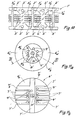
- the grid 1 is intended not only to form the contact pads of the modules but also to support the latter, to move them on a machine and to transfer them from one machine to another, this throughout their manufacture so that that - it can be done in the most automated way possible.
- the grid 1 has, on the one hand, in its central part, a plurality of identical openings 2 regularly distributed in the direction of its length and in each of which penetrate tabs 3 attached to one end to the frame 4 of the grid and free to the other which will constitute the contact pads and, on the other hand, along each of its edges, a series of equidistant perforations 5 which will allow it to be positioned and scrolled step by step in front of the different tools which will be used for the realization of the modules.
- the openings 2 are octagonal, the perforations 5 are located between these openings and the tongues 3 which are eight in number per opening all have the same rectangular shape and the same dimensions and are arranged at both parallel to the edges of the grid and symmetrically with respect to the median planes of the openings which are perpendicular to the latter.
- a ribbon is chosen which already has the qualities which the ranges of the modules must have, namely good resistance both to wear by contact or by friction and to atmospheric corrosion or by other agents capable of deteriorate them.
- It may, for example, be a nickel-plated and gilded copper ribbon or better still a stainless alloy such as nickel silver and in particular that which is marketed under the brand "ARCAP" by the French company ARCAP Anticorrosion and which is composed of '' about 56% copper, 25% nickel, 17% zinc and 2% additional metals.
- the pads 6 are preferably injection molded using a thermoplastic material which has substantially the same elasticity characteristics as that which will be used to manufacture the card bodies in which the modules will be inserted and which will most often be chloride.
- polyvinyl commonly designated by the abbreviation PVC.
- this material must be a very good electrical insulator and not risk losing this quality by absorbing water or other substances with which the cards can be brought into contact. It can be, for example, phenylene polysulfide (PPS) or another polysulfide, a polysulfone, a polycarbonate, a polyester which meets the requirements which have just been indicated.
- Each patch 6 is in the form of a disc slightly smaller than the openings 2 of the grid 1, one of the faces 6a of which is essentially flat and which has a circular central part 6, which is thicker than the peripheral part 6 d that surrounds it.
- the diameter of the central part 6 can be roughly half that of the disc and its thickness about one and a half times that of the peripheral part 6 d .
- the pellet has on the side of the flat face or front face 6a of the pellet of shallow grooves 7 which are provided to receive the tongues 3 of any of the openings of the grid.
- the also presented pellet on the side of its rear face 6b a recess 8 formed by a central area 8a and a series of grooves 8 b star which depart from this space and which extend to windows 9 which are provided between the recess and the front face 6a of the patch and which each open into one of the grooves 7.
- a cavity 10 intended to house an integrated circuit chip.
- each of these pellets is fixed by its front face 6a to the tongues 3 of an opening 2 of the grid, so that the latter are located in the grooves 7 of the pad provided to receive them, as shown in Figure 3.
- This fixing can be done by gluing or by heat-sealing but it is preferable for this to use the technique of ultrasonic welding which makes it possible to ensure a much more solid bond between the tongues and the pellet.
- the tabs 3 when after having brought a pellet opposite an opening of the grid, the tabs 3 will be pressed by subjecting them to ultrasonic vibrations, this will cause the plastic material to heat mainly in the vicinity of the pins and a softening of it in these areas.
- the pins can then easily penetrate into the material and when after the welding operation it has become solid again they will be firmly anchored there, especially if, rather than having just straight sides, they have the shape indicated above or an equivalent shape for example that of a trapezoid whose small base would be on the side of the tongue to which they are attached.
- the first solution consists in firstly sticking the chip 12 in its housing and then using the ' technique of connection by wire better known under the English name of "Wire Bonding" to weld a first fine wire for example in atumtnium first on a connection terminal of the chip which then appears. in the form of a pad and then on the corresponding tab of the grid, then solder a second wire on another terminal of the chip and on another tab and so on.
- connection tabs on its terminals which are then pads, which can be done using one of the techniques generally designated by the English expressions "Beam Lead”, “Tape Automated Bonding “(abbreviation TAB) and” Flip Chip “which are well known, then place the assembly in the recess 8 of the patch while sticking the chip in its housing, the connection tabs being of course arranged so to be in the grooves 8 b , and finally to weld the ends of these tabs on the tabs of the grid.
- the next phase illustrated by FIG. 7 consists in filling the recess 8 and the windows 9 of each patch, and possibly also the space which surrounds the chip in the cavity 10, with an adhesive, insulating, curable and preferably material. opaque to protect the chip 12 it contains against light at least until the module is inserted into a card.
- This material may for example be a resin based on silicone or on epoxy.
- This last operation can be carried out by the module manufacturer if he does not produce the cards himself, in which case these modules will be delivered in bulk, generally after being tested, or by the customer.
- Each module can then be glued in a correspondingly shaped housing provided in a card body for example as shown in Figure 9 and as is done most often, that is to say in the corner at the top and at left of this body when viewed from the front.
- This housing can be an opening if the module has the same thickness as the card body or a cavity if the module is thinner.
- the second solution has at least two advantages compared to the first: the chip and the conductors are better protected and the connection surface between the card body and the module being much larger, the latter will be less likely to peel off as a result of the frequent and more or less significant deformations to which the card will be subjected when it is used.
- This second embodiment is suitable when the substrate of the chip which carries the integrated circuit must be grounded.
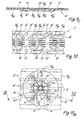
- the grid continues to present perforations 5 'for its drive, openings 2' and tongues 3 'which extend inside them, but in each group of tongues there is one which has a particular shape.
- This tab is formed of a straight main portion 3a which passes through the opening in which they are located in the middle and which is attached at both ends to the frame 4 'of the grid and of a branch 3b extending from this central part to go also attach to the frame and which replaces one of the tongues 3 of the grid of Figure 1.
- the other tongues 3 ' they keep the same shape and the same arrangement as before.
- each pellet is always in the form of a disc with a practically flat front face 64, a peripheral part 6 d thinner than the central part 6 c and a recess 8 'in the latter.
- one of the grooves 7 ' must also include a main part 7 a and a branch 7b so that their configuration is adapted to that of the tongues 3' of the grid 1 '.
- the second is that the cavity 10 of the chip for the integrated circuit chip has been replaced by an opening 10 'which opens into the main part 7a of the particular groove 7 and the third is due to the fact that the recess 8' of the pellet 6 'does not have exactly the same shape as that, 8, of pellet 6 since one of the windows 9' opens into the main part of the groove in question. In reality, this last difference is unimportant because we could very well remove it by opening this window in the ramification7b
- the following steps consist in fixing the pellets 6 'on the grid 1' (see FIG. 12), preferably using ultrasonic welding, in bonding chips 12 'in the housings 10 'who are reserved, to connect the connecting terminals 13 'of these chips to the tongues 3' of the conductors 14 ', according to one or other of the methods indicated above (see Figures 13a and 13b, Figure 13 b being a sectional view along the broken line XIII-XIII of Figure 13a) and filling the recesses 8 'with an insulating adhesive material 15' - (see Figure 14), but here the chips 12 'are bonded by means of a conductive adhesive on the main parts 3j of the particular tabs 3 'which, of course, are connected to their earth terminals.
- the first is to cut in one go all the tabs around each tablet. This can be done by the module manufacturer or by the customer provided that the latter can test these modules himself.
- the second which can often prove to be more advantageous and which is illustrated in FIG. 15, is to cut first only the tongues which, originally, had a free end, that is to say those which constitute the contact pads which are not connected to the earth terminal of a chip.
- the manufacturer who then takes care of this operation can, after having tested them, supply the modules in a strip to the customer who only has to cut the particular tabs in order to be able to insert the modules in cards.
- the grid could be in the form of a rectangular or square plate, with openings regularly distributed in rows and columns and which could be moved in two directions perpendicular to the different tools used for manufacturing modules.
- plastic pellets which define the shape of the modules could also be round. They could also be rectangular, square or other.
- each module not only one but two or more chips connected together, housed or not in the same cavity or opening of the bottom of the recess of the patch and of which at least one would be connected to the contact pads.
Abstract
Description
La présente invention a pour objet un procédé de fabrication de modules électroniques pour cartes à microcircuits telles que cartes de crédit, cartes bancaires, cartes de parking, cartes de paiement pour des appels téléphoniques dans des cabines publiques, etc., et les modules obtenus par la mise en oeuvre de ce procédé.The present invention relates to a method of manufacturing electronic modules for microcircuit cards such as credit cards, bank cards, parking cards, payment cards for telephone calls in public payphones, etc., and the modules obtained by the implementation of this process.
Telles qu'elles sont connues actuellement, les cartes à microcircuits appelées aussi cartes à mémoire ou cartes intelligentes comprennent généralement, comme circuit électronique, une mémoire et un microprocesseur intégrés sous forme d'une seule puce ou de deux puces connectées entre elles par des conducteurs électriques et un ensemble de plages de contact, souvent au nombre de huit, qui sont reliées au microprocesseur et qui sont accessibles pour les pièces de connexion d'un appareil, par exemple un terminal d'ordinateur, dans lequel la carte est destinée à être introduite.As currently known, microcircuit cards also called memory cards or smart cards generally include, as electronic circuit, a memory and a microprocessor integrated in the form of a single chip or two chips connected together by conductors electrical and a set of contact pads, often eight in number, which are connected to the microprocessor and which are accessible for the connection parts of a device, for example a computer terminal, in which the card is intended to be introduced.
Dans certains cas, ces différents éléments sont, à l'exception des plages de contact, noyés dans un corps isolant homogène ou composite pour former une pastille qui est ensuite placée dans une ouverture correspondante du corps de la carte. Dans d'autres, ils sont directement incorporés dans ce dernier.In certain cases, these various elements are, with the exception of the contact pads, embedded in a homogeneous or composite insulating body to form a patch which is then placed in a corresponding opening in the body of the card. In others, they are directly incorporated into the latter.
Indépendamment des questions liées au circuit intégré lui-même, comme par exemple celles de savoir quelles infomations la mémoire doit contenir, quelles fonctions doit remplir le microprocesseur, de quelle façon doivent être conçus cette mémoire et ce microprocesseur, l'introduction d'un circuit électronique dans une carte de transaction pose un certain nombre de problèmes, notamment à cause des exigences assez nombreuses auxquelles elles doivent répondre.Regardless of the questions related to the integrated circuit itself, such as for example those of knowing which information the memory must contain, which functions must fulfill the microprocessor, in which way this memory and this microprocessor must be designed, the introduction of a circuit Electronic in a transaction card poses a number of problems, in particular because of the fairly numerous requirements which they must meet.
Tout d'abord, une carte de paiement à microcircuits doit avoir le même format qu'une carte classique à pistes magnétiques standardisée dont la longueur est de 85 mm, la largeur de 54 mm et l'épaisseur de 0,76 mm (normes ISO) ou tout au moins des dimensions voisines pour rester peu encombrante et facilement maniable.First of all, a microcircuit payment card must have the same format as a conventional standardized magnetic stripe card, the length of which is 85 mm, the width of 54 mm and the thickness of 0.76 mm (ISO standards). ) or at least of the neighboring dimensions to remain compact and easy to handle.
Si l'on se rend compte que, premièrement, une épaisseur de 760 microns ne correspond grossièrement qu'à deux fois celle d'une puce de circuit intégré sans protection, que, deuxièmement, la portion de fa surface de la carte qui peut être allouée au circuit électronique est très limitée étant donné que la majeure partie de celle-ci doit être réservée à des inscriptions telles que la dénomination du prestataire qui délivre la carte, l'identité du porteur, une signature, des informations d'utilisation et éventuellement une photo et que, troisièmement, les plages conductrices doivent être suffisamment grandes pour que le contact avec les pièces de connexion d'un appareil soit assuré et bon, on en déduit très vite que l'on ne peut utiliser des circuits standardisés déjà enrobés ou emboîtés comme ceux que l'on trouve actuellement sur le marché et qui sont trop volumineux.If we realize that, first, a thickness of 760 microns roughly corresponds only to twice that of an unprotected integrated circuit chip, than, second, the portion of the surface of the card that can be allocated to the electronic circuit is very limited since the major part of it must be reserved for inscriptions such as the name of the service provider who issues the card, the identity of the holder, a signature, usage information and possibly a photo and that, thirdly, the conductive areas must be large enough for contact with the connection parts of a device to be ensured and good, it can be deduced very quickly that it is not possible to use standardized circuits already coated or nested like those currently found on the market and which are too bulky.
On est donc obligé, pour fabriquer les cartes ou les modules électroniques qui leur sont destinés, de partir de puces de circuits intégrés nues, de réaliser soi-même le réseau d'interconnexion qui permet de relier électriquement ces puces avec l'extérieur-et entre elles s'il y en a plusieurs dans une même carte et d'assurer la protection de l'ensemble qui est naturellement très fragile surtout au niveau des jonctions entre les pièces conductrices (bornes de connexion des puces, fils, etc.).It is therefore necessary, to manufacture the cards or the electronic modules which are intended for them, from bare integrated circuit chips, to make the interconnection network which makes it possible to electrically connect these chips with the outside and between them if there are several in the same card and to ensure the protection of the assembly which is naturally very fragile especially at the junctions between the conductive parts (connection terminals of the chips, wires, etc.).
Cette protection doit être d'autant plus efficace que les cartes seront forcément amenées à subir très souvent des déformations qui pourront être importantes du fait que l'on demande à ces cartes, comme aux cartes classiques, de répondre à des normes ou à des exigences de flexibilité relativement sévères et elle ne peut pas être assurée en donnant, aux modules électroniques ou aux zones des cartes dans lesquelles les circuits sont placés, la plus grande rigidité possible car les conditions de flexibilité en question ne seraient alors plus remplies.This protection must be all the more effective as the cards will inevitably be subjected to very often deformations which may be significant due to the fact that these cards, as with conventional cards, are asked to meet standards or requirements. of relatively severe flexibility and it cannot be ensured by giving, to the electronic modules or to the areas of the cards in which the circuits are placed, the greatest possible rigidity because the flexibility conditions in question would then no longer be met.
Par ailleurs, il faut éviter que des agents extérieurs, comme la lumière ou l'humidité puissent venir détériorer' le circuit ou en perturber le fonctionnement.In addition, care must be taken to prevent external agents, such as light or humidity, from damaging the circuit or disturbing its operation.
Enfin, il est bien clair que les cartes doivent pourvoir être fabriquées en grande série et à un prix de revient très bas, surtout s'il s'agit de cartes auxquelles est attribuée initialement une certaine valeur que l'on paie en les achetant et qui, lorsque cette valeur est épuisée, doivent tout simplement être jetées.Finally, it is very clear that the cards must be able to be produced in large series and at a very low cost price, especially if they are cards to which is initially attributed a certain value which one pays by buying them and which, when this value is exhausted, should simply be discarded.
Le but de l'invention est d'apporter une solution satisfaisante à ces différents problèmes.The object of the invention is to provide a satisfactory solution to these various problems.
Conformément à l'invention, pour fabriquer des modules électroniques qui peuvent être ensuite incorporés dans des corps de cartes et qui comprennent une puce de circuit intégré avec une face avant munie de bornes de connexion et une face arrière et un ensemble de plages de contact métalliques reliées chacune à l'une des bornes de connexion de la puce,
- -on se munit d'une grille métallique comportant une pluralité d'ouvertures identiques délimitées par un cadre et, dans chaque ouverture, un ensemble de languettes rattachées au cadre et destinées à former les plages de contact d'un module;
- -on se munit également d'une série de pastilles en matière synthétique plus petites que les ouvertures de la grille, chaque pastille ayant une face avant sensiblement plane, une face arrière du côté de laquelle elle présente un évidement et, entre cet évidement et ladite face avant, des fenêtres prévues pour pouvoir être amenées chacune au droit d'une languette d'un ensemble;
- -on fixe une pastille par sa face avant sur chaque ensemble de languettes de façon que les fenêtres en question se trouvent effectivement au droit de ces languettes;
- -on fixe une puce de circuit intégré au fond de l'évidement de chaque pastille de façon que sa face arrière soit orientée vers la grille;
- -on relie les bornes de connexion de la puce aux languettes sur lesquelles la pastille est fixée, au moyen de conducteurs logés dans l'évidement de la pastille et passant par les fenêtres; et
- -on remplit l'évidement et les fenêtres de chaque pastille d'un matériau adhésif durcissable électriquement isolant.
- - a metal grid is provided with a plurality of identical openings delimited by a frame and, in each opening, a set of tongues attached to the frame and intended to form the contact pads of a module;
- -on also a series of plastic pellets smaller than the grid openings, each tablet having a substantially planar front face, a rear face on the side of which it has a recess and, between this recess and said front face, windows provided to be able to be brought each to the right of a tongue of an assembly;
- - a patch is fixed by its front face on each set of tabs so that the windows in question are actually located at the right of these tabs;
- - an integrated circuit chip is fixed to the bottom of the recess of each patch so that its rear face is oriented towards the grid;
- -on connects the connection terminals of the chip to the tabs on which the patch is fixed, by means of conductors housed in the recess of the patch and passing through the windows; and
- - the recess and the windows of each pellet are filled with an electrically insulating curable adhesive material.
Pour fixer les puces à l'intérieur des pastilles et relier leurs bornes de connexion aux languettes, on peut soit commencer par coller chaque puce dans le fond de l'évidement d'une pastille et souder ensuite chaque conducteur d'abord sur une borne de connexion de cette puce puis sur la languette correspondante de la grille, soit commencer par souder les conducteurs par une de leurs extrémités sur les bornes de connexion des puces, coller ensuite ces dernières dans le fond des évidements des pastilles et enfin souder les autres extrémités des conducteurs sur les languettes.To fix the chips inside the pads and connect their connection terminals to the tabs, one can either start by sticking each chip in the bottom of the recess of a patch and then solder each conductor first on a terminal connection of this chip then on the corresponding tab of the grid, either start by soldering the conductors by one of their ends on the connection terminals of the chips, then paste the latter in the bottom of the recesses of the pads and finally solder the other ends of the conductors on the tabs.
Lorsque les modules sont terminés, on peut les détacher soi-même de la grille en découpant les languettes autour de chaque pastille, ou bien laisser ce soin à celui qui achète ces modules pour les incorporer dans des cartes.When the modules are finished, you can detach them yourself from the grid by cutting the tabs around each tablet, or leave it to the one who buys these modules to incorporate them into cards.
Ce procédé qui ne nécessite que peu d'opérations permet de réaliser des modules en très grand nombre, en partant de produits assez bon marché et en utilisant des techniques de fabrication que l'on maîtrise maintenant très bien dans le domaine de l'électronique. D'autres caractéristiques et avantages de l'in--ventibn apparaîtront au cours de la description détaillée mais non limitative qui suit de deux manières possibles de la mettre en oeuvre.This process, which requires only a few operations, makes it possible to produce modules in very large numbers, starting from fairly inexpensive products and using manufacturing techniques which are now very well mastered in the field of electronics. Other characteristics and advantages of the invention will become apparent during the detailed but non-limiting description which follows in two possible ways of implementing it.
Cette description sera faite en référence aux dessins annexés parmi lesquels :
- -la figure 1 montre partiellement, en plan, une grille que l'on fabrique conformément au premier de ces modes de mise en oeuvre de l'invention;
- -les figures 2a et 2b sont des vues respectivement de dos et de face d'une pastille en matière plastique qui est également réalisée conformément à ce même mode;
- -la figure 2c est une vue en coupe de la pastille selon la ligne brisée II-II de la figure 2a;
- -la figure 3 montre comment des pastilles comme celle des figures 2a à 2c sont fixées sur des languettes de la grille de la figure 1 qui sont destinées à former les plages de contact des modules;
- -la figure 4 est une vue partielle et agrandie de la grille de la figure 1 qui montre les ergots dont les languettes sont munies lorsque les pastilles sont soudées sur la grille par ultrasons;
- -la figure 5aest une vue partielle en plan d'une languette de la figure 4 qui permet de mieux montrer la forme des ergots;
- -la figure 5b montre, vue par le haut, la languette de la figure 5a, lorsque les ergots sont repliés à angle droit;
- -la figure 6a montre une pastille vue partiellement de dos, avec une puce de circuit intégré et les connexion entre les bornes de cette dernière et les languettes de la grille après que celles-ci aient été réalisées;
- -la figure 6b est une vue en coupe suivant la ligne brisée VI-VI de la figure 6a;
- -la figure 7 est une vue en coupe semblable à celle de la figure 6b qui montre un module terminé;
- -la figure 8 est une vue de face de ce dernier;
- -la figure 9 montre schématiquement le module incorporé dans une carte;
- -les figures 10, 11a, 11b, 11c, 12, 13a, 136 et 14 sont des vues analogues respectivement à celles des figures 1, 2a, 2 b, 2c, 3, 6a, 6b et 7 qui illustrent le deuxième mode de mise en oeuvre de l'invention; et
- -la figure 15 montre comment dans ce deuxième mode les modules peuvent être laissés attachés au cadre de la grille pour être testés et livrés en bande.
- FIG. 1 partially shows, in plan, a grid which is manufactured in accordance with the first of these embodiments of the invention;
- FIGS. 2a and 2b are respectively rear and front views of a plastic tablet which is also produced in accordance with this same mode;
- FIG 2 c is a sectional view of the pellet along the broken line II-II of Figure 2a;
- FIG. 3 shows how pellets like that of FIGS. 2a to 2 c are fixed on the tongues of the grid of FIG. 1 which are intended to form the contact pads of the modules;
- FIG. 4 is a partial and enlarged view of the grid of FIG. 1 which shows the pins with which the tongues are provided when the pellets are welded to the grid by ultrasound;
- FIG. 5 a is a partial plan view of a tab of FIG. 4 which makes it possible to better show the shape of the pins;
- FIG. 5b shows, seen from above, the tongue of FIG. 5a, when the lugs are folded at right angles;
- FIG. 6a shows a patch seen partially from the back, with an integrated circuit chip and the connections between the terminals of the latter and the tabs of the grid after these have been produced;
- FIG 6B is a sectional view along the broken line VI-VI of Figure 6a;
- FIG. 7 is a sectional view similar to that of FIG. 6 b which shows a completed module;
- FIG. 8 is a front view of the latter;
- FIG. 9 schematically shows the module incorporated in a card;
- FIGS. 10, 11a, 11b, 11c, 12, 13a, 13 6 and 14 are views similar respectively to those of FIGS. 1, 2a, 2b , 2c , 3, 6a, 6b and 7 which illustrate the second mode of implementing the invention; and
- FIG. 15 shows how in this second mode the modules can be left attached to the frame of the grid to be tested and delivered in a strip.
Pour réaliser des modules électroniques conformément au premier mode de mise en oeuvre du procédé selon l'invention que l'on a choisi de décrire, on commence par fabriquer une grille métallique 1 en forme de bande, comme celle que montre partiellement la figure 1 et des pastilles 6 en matière synthétique comme celle des figures 2a, 2bet2c.To produce electronic modules in accordance with the first embodiment of the method according to the invention which we have chosen to describe, we begin by manufacturing a
La grille 1 est destinée non seulement à former les plages de contact des modules mais également à supporter ces derniers, à les déplacer sur une machine et à les transférer d'une machine à une autre, ceci tout au long de leur fabrication afin que celle-ci puisse se faire de la manière la plus automatisée possible.The
Pour cela, la grille 1 présente, d'une part, dans sa partie centrale, une pluralité d'ouvertures identiques 2 régulièrement réparties dans le sens de sa longueur et dans chacune desquelles pénètrent des languettes 3 rattachées à un bout au cadre 4 de la grille et libres à l'autre qui constitueront les plages de contact et, d'autre part, le long de chacun de ses bords, une série de perforations équidistantes 5 qui permettront de la positionner et de la faire défiler pas à pas devant les différents outils qui seront utilisés pour la réalisation des modules.For this, the
Telles qu'elles sont représentées sur la figure, les ouvertures 2 sont octogonales, les perforations 5 se trouvent entre ces ouvertures et les languettes 3 qui sont au nombre de huit par ouverture ont toutes la même forme rectangulaire et les mêmes dimensions et sont disposées à la fois parallèlement aux bords de la grille et symétriquement par rapport aux plans médians des ouvertures qui sont perpendiculaires à ces derniers.As shown in the figure, the
Naturellement, ceci n'est qu'un exemple de configuration que peut avoir la grille. La forme des ouvertures et la position des perforations par rapport à celles-ci pourraient être différentes sans que cela change quoi que ce soit au procédé de fabrication des modules. Il en est de même en ce qui concerne le nombre des languettes, leur forme et leur disposition dans les ouvertures, bien que ceux qui ont été choisis correspondent en fait au dessin des plages de contact qui est actuellement le plus répandu et qui s'impose de plus en plus dans le cas des cartes de transactions.Naturally, this is only an example of the configuration that the grid can have. The shape of the openings and the position of the perforations with respect to them could be different without this changing anything in the manufacturing process of the modules. It is the same with regard to the number of tabs, their shape and their arrangement in the openings, although those which have been chosen correspond in fact to the design of the contact pads which is currently the most widespread and which is essential. more and more in the case of transaction cards.
Quel que soit le modèle de grille que l'on retient, on peut toujours réaliser celle-ci facilement en partant d'un ruban métallique que l'on découpe de façon classique, mécaniquement ou par attaque chimique.Whichever grid model we choose, we can always make it easily starting from a metal strip that we cut in a conventional way, mechanically or by chemical attack.
De préférence, on choisit un ruban qui possède déjà les qualités que devront présenter les plages des modules, à savoir une bonne résistance à la fois à l'usure par contact ou par frottement et à la corrosion atmosphérique ou par d'autres agents susceptibles de les détériorer.Preferably, a ribbon is chosen which already has the qualities which the ranges of the modules must have, namely good resistance both to wear by contact or by friction and to atmospheric corrosion or by other agents capable of deteriorate them.
Il peut s'agir par exemple d'un ruban de cuivre nickelé et doré ou mieux d'un alliage inoxydable comme le maillechort et notamment de celui que est commercialisé sous la marque "ARCAP" par la société française ARCAP Anticorrosion et qui se compose d'environ 56 % de cuivre, 25 % de nickel, 17 % de zinc et 2 % de métaux additionnels.It may, for example, be a nickel-plated and gilded copper ribbon or better still a stainless alloy such as nickel silver and in particular that which is marketed under the brand "ARCAP" by the French company ARCAP Anticorrosion and which is composed of '' about 56% copper, 25% nickel, 17% zinc and 2% additional metals.
Grâce à ce choix, on évite d'avoir à traiter galvaniquement sinon la grille toute entière, du moins les parties qui formeront les plages de contact.Thanks to this choice, we avoid having to galvanically treat if not the entire grid, at least the parts which will form the contact pads.
Quant aux pastilles 6, elles sont de préférence moulées par injection en utilisant une matière thermoplastique qui présente sensiblement les mêmes caractéristiques d'élasticité que celle qui servira à fabriquer les corps de cartes dans lesquels les modules seront insérés et qui sera le plus souvent du chlorure de polyvinyle désigné couramment par l'abréviation PVC. De plus, cette matière doit être un très bon isolant électrique et ne pas risquer de perdre cette qualité en absorbant de l'eau ou d'autres substances avec lesquelles les cartes pourront être amenées en contact. Il peut s'agir par exemple du polysulfure de phénylène (PPS) ou d'un autre polysulfure, d'un polysulfone, d'un polycarbonate, d'un polyester qui répond aux exigences qui viennent d'être indiquées.As for the
Chaque pastille 6 se présente sous la forme d'un disque légèrement plus petit que les ouvertures 2 de la grille 1, dont l'une des faces 6a est essentiellement plane et qui a une partie centrale circulaire 6, plus épaisse que la partie périphérique 6d qui l'entoure. Par exemple, le diamètre de la partie centrale 6, peut être, en gros, la moitié de celui du disque et son épaisseur environ une fois et demi celle de la partie périphérique 6d.Each
Comme le montre la figure 2b, la pastille présente du côté de la face plane ou face avant 6a de la pastille des gorges 7 peu profondes qui sont prévues pour recevoir les languettes 3 de l'une quelconque des ouvertures de la grille.As shown in Figure 2b , the pellet has on the side of the flat face or front face 6a of the pellet of
La forme, la grandeur et la profondeur de ces gorges sont telles que les languettes puissent les combler totalement, sans en sortir.The shape, size and depth of these grooves are such that the tongues can completely fill them, without coming out.
Par ailleurs, comme on peut le voir sur les figures 2a et 2c, la pastille présenté également du côté de sa face arrière 6 b un évidement 8 formé par un espace central 8a et par une série de rainures 8b en étoile qui partent de cet espace et qui se prolongent jusqu'à des fenêtres 9 qui sont prévues entre l'évidement et la face avant 6a de la pastille et qui débouchent chacune dans l'une des gorges 7.Furthermore, as can be seen in Figures 2a and 2c, the also presented pellet on the side of its rear face 6b a
Enfin, au fond de l'évidement 8 et au centre de celui-ci se trouve une cavité 10 destinée à loger une puce de circuit intégré.Finally, at the bottom of the
A noter que l'on pourrait aussi imaginer de donner à l'évidement 8 une forme plus simple, par exemple ronde ou rectangulaire, les fenêtres 9 continuant à se trouver au fond de celui-ci.Note that one could also imagine giving the recess 8 a simpler shape, for example round or rectangular, the
Lorsque l'on dispose de la grille 1 et des pastilles 6, on fixe chacune de ces pastilles par sa face avant 6a sur les languettes 3 d'une ouverture 2 de la grille, de façon que ces dernières se trouvent dans les gorges 7 de la pastille prévues pour les recevoir, comme le montre la figure 3.When the
Cette fixation peut se faire par collage ou par thermosoudage mais il est préférable pour cela de faire appel à la technique du soudage par ultrasons qui permet d'assurer une liaison beaucoup plus solide entre les languettes et la pastille.This fixing can be done by gluing or by heat-sealing but it is preferable for this to use the technique of ultrasonic welding which makes it possible to ensure a much more solid bond between the tongues and the pellet.
Si l'on décide d'utiliser effectivement cette méthode de soudage, on prévoit au moment de la réalisation de la grille des ergots 11 répartis autour de chaque languette, comme on peut le voir sur la vue agrandie de la figure 4. Il peut y avoir par exemple cinq ergots par languette, deux de chaque côté de celle-ci et un au bout.If one decides to actually use this welding method, provision is made at the time of the production of the lugs lugs 11 distributed around each tongue, as can be seen in the enlarged view of FIG. 4. There may be For example, have five lugs per tab, two on each side of it and one at the end.
Pour une raison qui apparaîtra par la suite, il est avantageux de donner aux côtés de ces ergots une forme incurvée ou en V, comme le montre la figure 5a, de façon qu'ils soient plus étroits au centre qu'aux extrémités.For a reason which will appear later, it is advantageous to give the sides of these lugs a curved or V shape, as shown in FIG. 5a, so that they are narrower in the center than at the ends.
Après que la grille ait été découpée, ces ergots sont repliés à 90° du côté où se trouveront les pastilles, ce qui est illustré par la figure 5b.After the grid has been cut, these pins are folded 90 ° to the side where the pellets will be, which is illustrated in Figure 5b .
Ainsi, lorsqu'après avoir amené une pastille en regard d'une ouverture de la grille, on pressera sur les languettes 3 en les soumettant à des vibrations ultrasonores, cela provoquera un échauffement de la matière plastique principalement au voisinage des ergots et un ramollissement de celle-ci dans ces zones. Les ergots pourront alors pénétrer facilement dans la matière et lorsqu'après l'opération de soudage celle-ci sera redevenue solide ils y seront solidement ancrés, surtout si, plutôt que d'avoir simplement des côtés droits, ils ont la forme indiquée précédemment ou une forme équivalente par exemple celle d'un trapèze dont la petite base se trouverait du côté de la languette à laquelle ils sont rattachés.Thus, when after having brought a pellet opposite an opening of the grid, the
Suivant l'appareillage dont on dispose ou que l'on a prévu pour fabriquer les modules, on peut soit fixer d'abord toutes les pastilles sur la grille avant de passer à la phase suivante et faire ensuite -de même pour toutes les autres opérations, soit utiliser la méthode du travail à la chaîne, c'est-à-dire ne pas attendre qu'une opération soit complètement terminée pour commencer la suivante et arriver ainsi à en exécuter plusieurs en même temps sur des unités différentes. Pour la suite, on supposera que l'on se trouve dans le premier cas.Depending on the equipment available or planned for manufacturing the modules, you can either fix all the pellets on the grid first before going to the next phase and then do the same for all other operations , or use the chain work method, that is to say, do not wait until one operation is completely finished to start the next and thus manage to execute several at the same time on different units. For the rest, we will assume that we are in the first case.
Donc, après avoir fixé les pastilles sur la grille, il s'agit de coller dans le logement 10 de chacune de celle-ci qui lui est réservé une puce de circuit intégré 12 (voir figures 6a et 6b) de façon naturellement que sa face avant munie de bornes de connexion 13 se trouve du côté opposé à la grille et de relier chacune de ces bornes à une languette 3, en faisant passer un conducteur 14 dans une rainure 8b et dans l'ouverture correspondante 9 et en veillant à ce qu'aucune partie de ce conducteur ne sorte de l'évidement 8.So, after having fixed the pellets on the grid, it is a question of sticking in the
Pour cela on peut procéder de deux façons. La première solution consiste à coller tout d'abord la puce 12 dans son logement et à utiliser ensuite la 'technique de la connexion par fil plus connu sous l'appellation anglaise de "Wire Bonding" pour souder un premier fil fin par exemple en atumtnium d'abord sur une borne de connexion de la puce qui se présente alors . sous la forme d'une plage et ensuite sur la languette correspondante de la grille, puis souder un deuxième fil sur une autre borne de la puce et sur une autre languette et ainsi de suite.There are two ways to do this. The first solution consists in firstly sticking the
L'autre possibilité est de commencer par munir la puce de pattes de connexion soudées sur ses bornes qui sont alors des plots, ce qui peut être fait en employant l'une des techniques désignées généralement par les expressions anglaises "Beam Lead", "Tape Automated Bonding" (abréviation T.A.B.) et "Flip Chip" qui sont bien connues, de placer ensuite l'ensemble dans l'évidement 8 de la pastille tout en collant la puce dans son logement, les pattes de connexion étant bien entendu disposées de façon à se trouver dans les rainures 8b, et enfin de souder les extrémités de ces pattes sur les languettes de la grille.The other possibility is to start by providing the chip with soldered connection tabs on its terminals which are then pads, which can be done using one of the techniques generally designated by the English expressions "Beam Lead", "Tape Automated Bonding "(abbreviation TAB) and" Flip Chip "which are well known, then place the assembly in the
La phase suivante illustrée par la figure 7 consiste à remplir l'évidement 8 et les fenêtres 9 de chaque pastille, et éventuellement aussi l'espace qui entoure la puce dans la cavité 10, d'un matériau adhésif, isolant, durcissable et de préférence opaque pour protéger la puce 12 qu'elle contient contre la lumière au moins jusqu'à ce que le module soit inséré dans une carte. Ce matériau peut être par exemple une résine à base de silicone ou d'époxyde.The next phase illustrated by FIG. 7 consists in filling the
Il ne reste plus alors qu'à découper les languettes 3 en suivant le contour de chaque pastille 6 pour obtenir une série de modules comme celui qui est représenté, vu de face, sur la figure 8.It then only remains to cut the
Cette dernière opération peut être exécutée par le fabricant de modules s'il ne produit pas lui-même les cartes, auquel cas ces modules seront livrés en vrac, généralement après avoir été testés, ou par le client.This last operation can be carried out by the module manufacturer if he does not produce the cards himself, in which case these modules will be delivered in bulk, generally after being tested, or by the customer.
Chaque module peut être ensuite collé dans un logement de forme correspondante prévu dans un corps de carte par exemple comme le montre la figure 9 et comme cela se fait le plus souvent, c'est-à-dire dans le coin situé en haut et à gauche de ce corps lorsqu'il est vu de face.Each module can then be glued in a correspondingly shaped housing provided in a card body for example as shown in Figure 9 and as is done most often, that is to say in the corner at the top and at left of this body when viewed from the front.
Ce logement peut être une ouverture si le module a la même épaisseur que le corps de carte ou une cavité si le module est plus mince. La deuxième solution présente au moins deux avantages par rapport à la première : la puce et les conducteurs sont mieux protégés et la surface de liaison entre Je corps de carte et le module étant beaucoup plus grande, ce dernier risquera moins de se décoller par suite des déformations fréquentes et plus ou moins importantes auxquelles la carte sera soumise lorsqu'elle sera utilisée.This housing can be an opening if the module has the same thickness as the card body or a cavity if the module is thinner. The second solution has at least two advantages compared to the first: the chip and the conductors are better protected and the connection surface between the card body and the module being much larger, the latter will be less likely to peel off as a result of the frequent and more or less significant deformations to which the card will be subjected when it is used.
Enfin, pour en terminer avec ce premier mode de mise en oeuvre du procédé selon l'invention, il reste à indiquer pourquoi on a choisi de réaliser les modules sous la forme de disques plus épais au centre qu'à la périphérie plutôt qu'avec deux faces planes parallèles. La raison est que, de ce fait, les contraintes que subira le corps de carte lorsque celle-ci sera soumise à des flexions ou à des torsions seront sinon annihilées du moins très atténuées au niveau de la frontière entre les parties mince et épaisse du disque. La puce de circuit intégré, les conducteurs et les soudures au niveau des bornes de connexion de la puce et des plages de contact seront donc beaucoup mieux protogés du point de vue mécanique.Finally, to finish with this first mode of implementation of the method according to the invention, it remains to indicate why we chose to produce the modules in the form of thicker discs in the center than at the periphery rather than with two parallel flat faces. The reason is that, as a result, the stresses which the card body will undergo when it is subjected to bending or twisting will be otherwise eliminated at least very attenuated at the level of the border between the thin and thick parts of the disc. . The integrated circuit chip, the conductors and the solderings at the connection terminals of the chip and the contact pads will therefore be much better protected from the mechanical point of view.
Le deuxième mode de mise en oeuvre de l'invention dont il va être question maintenant présente en fait beaucoup de points communs avec le premier. On s'emploiera donc surtout à préciser les différences qui existent entre les deux.The second embodiment of the invention which will now be discussed in fact has a lot in common with the first. We will therefore focus on clarifying the differences between the two.
D'autre part, les mêmes objets ou parties de ceux-ci qui sont identiques ou équivalents à ceux ou celles dont il a été question jusqu'à présent seront désignés par les mêmes repères avec en plus le signe""'.On the other hand, the same objects or parts thereof which are identical or equivalent to those which have been discussed so far will be designated by the same references with in addition the sign "" '.
Ce deuxième mode de mise en oeuvre convient lorsque le substrat de la puce qui porte le circuit intégré doit être mis à la masse.This second embodiment is suitable when the substrate of the chip which carries the integrated circuit must be grounded.
Ici encore, on commence par réaliser, d'une part, une grille 1' en forme de bande comme celle qui est représentée sur la figure 10 et, d'autre part, des pastilles 6' en matière synthétique comme celle qui est montrée de dos et de face respectivement sur les figures 11a et 11b b et en coupe suivant la ligne brisée XI-XI de la figure 11 a sur la figure 11c.Here again, we begin by making, on the one hand, a
La grille l' continue à présenter des perforations 5' pour son entraînement, des ouvertures 2' et des languettes 3' qui s'étendent à l'intérieur de celles-ci, mais dans chaque groupe de languettes il y en a une qui a une forme particulière. Cette languette est formée d'une partie principale droite 3a qui traverse l'ouverture dans laquelle elles se trouve en son milieu et qui est rattachée aux deux bouts au cadre 4' de la grille et d'une ramification 3b qui part de cette partie centrale pour aller se rattacher elle aussi au cadre et qui remplace l'une des languettes 3 de la grille de la figure 1. Quant aux autres languettes 3', elles conservent la même forme et la même disposition que précédemm'ent.The grid continues to present perforations 5 'for its drive, openings 2' and tongues 3 'which extend inside them, but in each group of tongues there is one which has a particular shape. This tab is formed of a straight main portion 3a which passes through the opening in which they are located in the middle and which is attached at both ends to the frame 4 'of the grid and of a branch 3b extending from this central part to go also attach to the frame and which replaces one of the
Par ailleurs, chaque pastille se présente toujours sous la forme d'un disque avec une face avant 64 pratiquement plane, une partie périphérique 6d plus mince que la partie centrale 6c et un évidement 8' dans cette dernière.Furthermore, each pellet is always in the form of a disc with a practically flat front face 64, a
Cependant, si l'on compare la pastille 6' des figures 11 a à 11cavec celle, 6, des figures 2 a à 2c, on voit qu'il y a trois différences.However, if we compare the
La première qui concerne les gorges que présentent les faces avant de ces pastilles s'impose. Il est clair en effet que l'une des gorges 7' doit comporter, elle aussi, une partie principale 7a et une ramification 7b pour que leur configuration soit adaptée à celle des languettes 3' de la grille 1'.The first which concerns the grooves presented by the front faces of these pellets is essential. It is clear in fact that one of the
La deuxième est que la cavité 10 de la pastille pour la puce de circuit intégré a été remplacée par une ouverture 10' qui débouche dans la partie principale 7a de la gorge 7 particulière et la troisième tient au fait que l'évidement 8' de la pastille 6' n'a pas exactement la même forme que celui, 8, de la pastille 6 étant donné que l'une des fenêtres 9' débouche dans la partie principale de la gorge en question. En réalité, cette dernière différence est sans importance car on pourrait très bien la supprimer en faisant déboucher cette fenêtre dans la ramification7bThe second is that the
Comme dans le premier mode de mise en oeuvre, les étapes sui vantes consistent à fixer la pastilles 6' sur la grille 1' (voir figure 12), en utilisant de préférence le soudage par ultrasons, à coller des puces 12' dans les logements 10' qui leur sont réservés, à relier les bornes de connexion 13' de ces puces aux languettes 3' par des conducteurs 14', selon l'une ou l'autre des méthodes indiquées ci-dessus (voir figures 13a et 13b, la figure 13b étant une vue en coupe suivant la ligne brisée XIII-XIII de la figure 13a) et à combler les évidements 8' d'un matériau adhésif isolant 15' - (voir figure 14), mais ici les puces 12' sont collées au moyen d'une colle conductrice sur les parties principales 3j des languettes 3' particulières qui, bien entendu, sont connectées à leurs bornes de masse.As in the first embodiment, the following steps consist in fixing the pellets 6 'on the grid 1' (see FIG. 12), preferably using ultrasonic welding, in bonding chips 12 'in the housings 10 'who are reserved, to connect the connecting terminals 13 'of these chips to the tongues 3' of the conductors 14 ', according to one or other of the methods indicated above (see Figures 13a and 13b, Figure 13 b being a sectional view along the broken line XIII-XIII of Figure 13a) and filling the recesses 8 'with an insulating adhesive material 15' - (see Figure 14), but here the chips 12 'are bonded by means of a conductive adhesive on the main parts 3j of the particular tabs 3 'which, of course, are connected to their earth terminals.
Il ne reste plus ensuite qu'à séparer les modules de la grille et il y a pour cela deux possibilités.It then only remains to separate the modules from the grid and there are two possibilities for this.
La première est de découper en une seule fois toutes les languettes autour de chaque pastille. Ceci peut être fait par le fabricant de modules ou par le client à condition que celui-ci puisse tester lui-même ces modules.The first is to cut in one go all the tabs around each tablet. This can be done by the module manufacturer or by the customer provided that the latter can test these modules himself.
La deuxième qui peut s'avérer souvent plus avantageuse et qui est illustrée par la figure 15 est de ne découper d'abord que les languettes qui, à l'origine, avaient une extrémité libre c'est-à-dire celles qui constituent les plages de contact qui ne sont pas reliées à la borne de masse d'une puce. La fabricant qui se charge alors de cette opération peut, après les avoir testés, fournir les modules en bande au client qui n'a plus qu'à découper les languettes particulières pour pouvoir insérer les modules dans des cartes.The second, which can often prove to be more advantageous and which is illustrated in FIG. 15, is to cut first only the tongues which, originally, had a free end, that is to say those which constitute the contact pads which are not connected to the earth terminal of a chip. The manufacturer who then takes care of this operation can, after having tested them, supply the modules in a strip to the customer who only has to cut the particular tabs in order to be able to insert the modules in cards.
Bien qu'elle ne soit pas exclue, cette deuxième solution n'a pas été envisagée dans le cadre du premier mode de mise en oeuvre car, dans ce cas, les modules ne seraient plus soutenus après la première phase de découpage que par une languette rattachée seulement par un bout à la grille, qui risquerait de se casser ou de s'arracher au moins partiellement de la pastille à laquelle elle est liée et la livraison en bande de ces modules ne pourrait pas s'effectuer sans précautions particulières.Although it is not excluded, this second solution was not considered in the context of the first mode of implementation because, in this case, the modules would no longer be supported after the first cutting phase except by a tongue attached only by one end to the grid, which would risk breaking or at least partially tearing off the patch to which it is linked and the delivery in strips of these modules could not be carried out without special precautions.
Par contre, avec une languette qui reste fixée en trois points à la grille il n'y a plus ce problème. Naturellement, l'invention n'est pas limitée aux deux modes de mise en oeuvre qui viennent d'être décrits.On the other hand, with a tab which remains fixed at three points to the grid there is no longer this problem. Naturally, the invention is not limited to the two modes of implementation which have just been described.
Par exemple, plutôt que sous la forme d'une bande, la grille pourrait se présenter sous celle d'une plaque rectangulaire ou carrée, avec des ouvertures régulièrement réparties en lignes et en colonnes et qui pourrait être déplacée dans deux directions perpendiculaires devant les différents outils utilisés pour la fabrication de modules.For example, rather than in the form of a strip, the grid could be in the form of a rectangular or square plate, with openings regularly distributed in rows and columns and which could be moved in two directions perpendicular to the different tools used for manufacturing modules.
De même, il n'est pas obligatoire que les pastilles en matière synthétique qui définissent la forme des modules soient rondes. Elles pourraient aussi être rectangulaires, carrées ou autres.Likewise, it is not compulsory for the plastic pellets which define the shape of the modules to be round. They could also be rectangular, square or other.
Il peut arriver également, lorsqu'il n'y a pas besoin de mettre le substrat du circuit intégré à la masse, que la différence d'épaisseur entre la pastille et la puce soit suffisamment importante pour que l'on ne soit pas obligé de prévoir une cavité pour loger cette dernière et qu'on puisse la coller sur le fond alors plat de l'évidement de la pastille.It can also happen, when there is no need to ground the integrated circuit substrate, that the difference in thickness between the chip and the chip is large enough that it is not necessary to provide a cavity to accommodate the latter and that it can be glued to the flat bottom of the recess of the pellet.
Par ailleurs, on a indiqué les avantages que présente le fait qu'il y ait une différence d'épaisseur entre les parties centrale et périphérique des pastilles mais cela n'exclut pas la possibilité de donner à ces pastilles une épaisseur constante.Furthermore, the advantages presented by the fact that there is a difference in thickness between the central and peripheral parts of the pellets have been indicated, but this does not exclude the possibility of giving these pellets a constant thickness.
En ce qui concerne les gorges qui sont destinées à recevoir les languettes, il est clair que leur présence est très utile car elles permettent aux modules d'avoir une face avant parfaitement plane et de ne pas pouvoir être accusés de créer des surépaisseurs lorsqu'ils sont placés dans des cartes. De plus, grâce à elles il n'y a pas le risque que les plages de contact soient arrachées lorsqu'elles sont simplement collées ou fixées par thermosoudage sur les pastilles. Malgré cela, on peut quand même envisager de les supprimer.With regard to the grooves which are intended to receive the tongues, it is clear that their presence is very useful because they allow the modules to have a perfectly flat front face and not to be able to be accused of creating extra thicknesses when are placed in cards. In addition, thanks to them there is no risk that the contact pads are torn off when they are simply glued or fixed by heat sealing on the pellets. Despite this, we can still consider removing them.
D'autre part, au lieu de souder les extrémités des conducteurs sur les bornes de connexion des puces et sur les languettes, on pourrait les coller en utilisant une colle conductrice.On the other hand, instead of soldering the ends of the conductors on the connection terminals of the chips and on the tabs, they could be glued using a conductive adhesive.
Enfin, il est évident que l'on pourrait prévoir dans chaque module non pas une seule mais deux puces ou plus connectées entre elles, logées ou non dans la même cavité ou ouverture du fond de l'évidement de la pastille et dont une au moins serait reliée aux plages de contact.Finally, it is obvious that one could provide in each module not only one but two or more chips connected together, housed or not in the same cavity or opening of the bottom of the recess of the patch and of which at least one would be connected to the contact pads.
Claims (34)
Priority Applications (1)
| Application Number | Priority Date | Filing Date | Title |
|---|---|---|---|
| AT86104178T ATE54030T1 (en) | 1985-04-02 | 1986-03-26 | METHOD OF MANUFACTURE OF ELECTRONIC MODULES FOR CARDS WITH MICROSCIRCUITS AND MODULES MANUFACTURED IN THE WAY. |
Applications Claiming Priority (2)
| Application Number | Priority Date | Filing Date | Title |
|---|---|---|---|
| FR8505109 | 1985-04-02 | ||
| FR8505109A FR2579798B1 (en) | 1985-04-02 | 1985-04-02 | METHOD FOR MANUFACTURING ELECTRONIC MODULES FOR MICROCIRCUIT CARDS AND MODULES OBTAINED ACCORDING TO THIS METHOD |
Publications (3)
| Publication Number | Publication Date |
|---|---|
| EP0197438A1 true EP0197438A1 (en) | 1986-10-15 |
| EP0197438B1 EP0197438B1 (en) | 1990-06-20 |
| EP0197438B2 EP0197438B2 (en) | 1995-08-23 |
Family
ID=9317932
Family Applications (1)
| Application Number | Title | Priority Date | Filing Date |
|---|---|---|---|
| EP86104178A Expired - Lifetime EP0197438B2 (en) | 1985-04-02 | 1986-03-26 | Method of manufacturing electronic modules for microcircuit boards and modules obtained by this method |
Country Status (7)
| Country | Link |
|---|---|
| US (1) | US4674175A (en) |
| EP (1) | EP0197438B2 (en) |
| JP (1) | JPS61232629A (en) |
| AT (1) | ATE54030T1 (en) |
| DE (1) | DE3672171D1 (en) |
| FR (1) | FR2579798B1 (en) |
| HK (1) | HK93993A (en) |
Cited By (18)
| Publication number | Priority date | Publication date | Assignee | Title |
|---|---|---|---|---|
| FR2624652A1 (en) * | 1987-12-14 | 1989-06-16 | Sgs Thomson Microelectronics | METHOD FOR THE INSTALLATION ON A SUPPORT OF AN ELECTRONIC COMPONENT HAVING ITS CONTACTS |
| EP0344058A1 (en) * | 1988-05-25 | 1989-11-29 | Schlumberger Industries | Process for producing an electronic memory card, and electronic memory card obtained by using this process |
| FR2636453A1 (en) * | 1988-09-14 | 1990-03-16 | Sgs Thomson Microelectronics | METHOD FOR ENCAPSULATING INTEGRATED CIRCUITS, IN PARTICULAR FOR CARDS WITH CHIPS |
| FR2639763A1 (en) * | 1988-11-29 | 1990-06-01 | Schlumberger Ind Sa | METHOD FOR PRODUCING AN ELECTRONIC MODULE AND ELECTRONIC MODULE AS OBTAINED BY THIS METHOD |
| FR2644630A1 (en) * | 1989-03-20 | 1990-09-21 | Sgs Thomson Microelectronics | Process for encarding micromodules and its application to the production of microchip cards |
| EP0391790A1 (en) * | 1989-04-07 | 1990-10-10 | STMicroelectronics S.A. | Method of manufacturing an electronic module |
| EP0399868A2 (en) * | 1989-05-26 | 1990-11-28 | ESEC (Far East) Limited | Manufacturing process of a chip card and card obtained by this process |
| FR2647571A1 (en) * | 1989-05-26 | 1990-11-30 | Lemaire Gerard | Method of fabricating a card known as a chip card, and card obtained by this method |
| WO1991001533A1 (en) * | 1989-07-24 | 1991-02-07 | Edgar Schneider | Substrate element with at least one integrated circuit, in particular a substrate element for inclusion in chip cards |
| EP0424530A1 (en) * | 1988-07-08 | 1991-05-02 | Oki Electric Industry Company, Limited | Resin-sealed semiconductor device |
| US5047368A (en) * | 1986-01-31 | 1991-09-10 | U.S. Philips Corporation | Method of manufacturing a thick-film circuit arrangement |
| FR2673042A1 (en) * | 1991-02-18 | 1992-08-21 | Em Microelectronic Marin Sa | Electronic module resisting mechanical deformation, for a microcircuit card |
| EP0554916A2 (en) * | 1986-11-20 | 1993-08-11 | GAO Gesellschaft für Automation und Organisation mbH | Module with integrated circuits |
| EP0591668A1 (en) * | 1992-09-29 | 1994-04-13 | Siemens Aktiengesellschaft | Method of mounting semiconductor integrated circuits |
| EP0599194A1 (en) * | 1992-11-27 | 1994-06-01 | Esec Sempac S.A. | Flat-card-shaped electronic module |
| FR2738077A1 (en) * | 1995-08-23 | 1997-02-28 | Schlumberger Ind Sa | ELECTRONIC MICRO-BOX FOR ELECTRONIC MEMORY CARD AND EMBODIMENT PROCESS |
| USRE35578E (en) * | 1988-12-12 | 1997-08-12 | Sgs-Thomson Microelectronics, Inc. | Method to install an electronic component and its electrical connections on a support, and product obtained thereby |
| FR2957443A1 (en) * | 2010-03-12 | 2011-09-16 | Oberthur Technologies | Microcircuit card i.e. integrated circuit chip card, has connection wire connected to back of side pad for conveying electric signal associated with side pad that is electrically connected with central pad |
Families Citing this family (48)
| Publication number | Priority date | Publication date | Assignee | Title |
|---|---|---|---|---|
| US4996411A (en) * | 1986-07-24 | 1991-02-26 | Schlumberger Industries | Method of manufacturing a card having electronic memory and a card obtained by performing said method |
| DK436986A (en) * | 1986-09-12 | 1988-04-27 | Modulex As | CONNECTOR WITH A NUMBER OF ELECTRICAL CONNECTIONS, PROCEDURE FOR MAKING SUCH A PLATE AND USING THE CONNECTOR TO A PLANNING BOARD |
| US4835120A (en) * | 1987-01-12 | 1989-05-30 | Debendra Mallik | Method of making a multilayer molded plastic IC package |
| JP2904785B2 (en) * | 1987-01-26 | 1999-06-14 | 大日本印刷株式会社 | IC module with built-in card |
| FR2620586A1 (en) * | 1987-09-14 | 1989-03-17 | Em Microelectronic Marin Sa | METHOD FOR MANUFACTURING ELECTRONIC MODULES, IN PARTICULAR FOR MICROCIRCUIT CARDS |
| JPH0815829B2 (en) * | 1987-11-27 | 1996-02-21 | 松下電器産業株式会社 | Manufacturing method of IC card module |
| USRE35385E (en) * | 1988-12-12 | 1996-12-03 | Sgs-Thomson Microelectronics, Sa. | Method for fixing an electronic component and its contacts to a support |
| US6016255A (en) * | 1990-11-19 | 2000-01-18 | Dallas Semiconductor Corp. | Portable data carrier mounting system |
| JPH0521655A (en) * | 1990-11-28 | 1993-01-29 | Mitsubishi Electric Corp | Semiconductor device and package therefor |
| DE4143494C2 (en) * | 1990-11-28 | 1998-05-14 | Mitsubishi Electric Corp | Semiconductor device with reduced housing thickness and wt. |
| DE9100665U1 (en) * | 1991-01-21 | 1992-07-16 | Telbus Gesellschaft Fuer Elektronische Kommunikations-Systeme Mbh, 8057 Eching, De | |
| US5155065A (en) * | 1992-03-16 | 1992-10-13 | Motorola, Inc. | Universal pad pitch layout |
| DE4224103A1 (en) * | 1992-07-22 | 1994-01-27 | Manfred Dr Ing Michalk | Miniature housing with electronic components |
| DE4326816A1 (en) * | 1993-08-10 | 1995-02-16 | Giesecke & Devrient Gmbh | Electronic module for cards and manufacture of such a module |
| DE4401588C2 (en) * | 1994-01-20 | 2003-02-20 | Gemplus Gmbh | Method for capping a chip card module and chip card module |
| DE4421607A1 (en) * | 1994-06-21 | 1996-01-04 | Giesecke & Devrient Gmbh | Process for the production of data carriers |
| US5682143A (en) * | 1994-09-09 | 1997-10-28 | International Business Machines Corporation | Radio frequency identification tag |
| US5528222A (en) * | 1994-09-09 | 1996-06-18 | International Business Machines Corporation | Radio frequency circuit and memory in thin flexible package |
| US5671525A (en) * | 1995-02-13 | 1997-09-30 | Gemplus Card International | Method of manufacturing a hybrid chip card |
| DE19515189C2 (en) * | 1995-04-25 | 2003-07-10 | Infineon Technologies Ag | Chip cover |
| DE19515187C2 (en) * | 1995-04-25 | 2003-07-10 | Infineon Technologies Ag | Chip cover |
| FR2733848B1 (en) * | 1995-05-05 | 1997-05-30 | Schlumberger Ind Sa | COATING PROCESS FOR AN ELECTRONIC COMPONENT AND DEVICE FOR IMPLEMENTING THE SAID PROCESS |
| FR2736740A1 (en) * | 1995-07-11 | 1997-01-17 | Trt Telecom Radio Electr | PROCESS FOR PRODUCING AND ASSEMBLING INTEGRATED CIRCUIT BOARD AND CARD THUS OBTAINED |
| DE19543427C2 (en) * | 1995-11-21 | 2003-01-30 | Infineon Technologies Ag | Chip module, in particular for installation in a chip card |
| GB9606453D0 (en) * | 1996-03-27 | 1996-06-05 | Clariant Finance Bvi Ltd | Improvements in or relating to organic compounds |
| DE19639025C2 (en) * | 1996-09-23 | 1999-10-28 | Siemens Ag | Chip module and method for producing a chip module |
| EP0845755B1 (en) * | 1996-12-02 | 2004-03-10 | Swisscom Mobile AG | IC-card and program for IC-cards |
| FR2778769B1 (en) * | 1998-05-15 | 2001-11-02 | Gemplus Sca | INTEGRATED CIRCUIT CARD INCLUDING AN INTERFACE TERMINAL BLOCK AND PROCESS FOR MANUFACTURING SUCH A CARD |
| DE19844966A1 (en) * | 1998-09-30 | 2000-01-13 | Siemens Ag | Semiconductor element for chip card module |
| FR2791812B1 (en) * | 1999-04-02 | 2002-01-25 | Gemplus Card Int | METHOD FOR MANUFACTURING PORTABLE ELECTRONIC DEVICES WITH INTEGRATED CIRCUIT PROTECTED BY A SPRAY FILM |
| TW449796B (en) * | 2000-08-02 | 2001-08-11 | Chiou Wen Wen | Manufacturing method for integrated circuit module |
| US6624005B1 (en) * | 2000-09-06 | 2003-09-23 | Amkor Technology, Inc. | Semiconductor memory cards and method of making same |
| US6734552B2 (en) | 2001-07-11 | 2004-05-11 | Asat Limited | Enhanced thermal dissipation integrated circuit package |
| US7015072B2 (en) | 2001-07-11 | 2006-03-21 | Asat Limited | Method of manufacturing an enhanced thermal dissipation integrated circuit package |
| US6790710B2 (en) * | 2002-01-31 | 2004-09-14 | Asat Limited | Method of manufacturing an integrated circuit package |
| US20030178719A1 (en) * | 2002-03-22 | 2003-09-25 | Combs Edward G. | Enhanced thermal dissipation integrated circuit package and method of manufacturing enhanced thermal dissipation integrated circuit package |
| US6940154B2 (en) * | 2002-06-24 | 2005-09-06 | Asat Limited | Integrated circuit package and method of manufacturing the integrated circuit package |
| JP4166065B2 (en) * | 2002-09-27 | 2008-10-15 | 三洋電機株式会社 | Circuit device manufacturing method |
| JP4645071B2 (en) * | 2003-06-20 | 2011-03-09 | 日亜化学工業株式会社 | Package molded body and semiconductor device using the same |
| JP2005093616A (en) * | 2003-09-16 | 2005-04-07 | Renesas Technology Corp | Semiconductor device and its manufacturing method |
| US20080179404A1 (en) * | 2006-09-26 | 2008-07-31 | Advanced Microelectronic And Automation Technology Ltd. | Methods and apparatuses to produce inlays with transponders |
| EP1928024A1 (en) * | 2006-12-01 | 2008-06-04 | Axalto SA | Carrier film for chip modules which is adapted for automatic control of wiring and method of manufacturing chip modules |
| JP2008251793A (en) * | 2007-03-30 | 2008-10-16 | Diamond Electric Mfg Co Ltd | Insert mold |
| GB0817865D0 (en) * | 2008-10-01 | 2008-11-05 | Optaglio Sro | Embedded element and related method |
| US8649820B2 (en) | 2011-11-07 | 2014-02-11 | Blackberry Limited | Universal integrated circuit card apparatus and related methods |
| US8936199B2 (en) | 2012-04-13 | 2015-01-20 | Blackberry Limited | UICC apparatus and related methods |
| USD703208S1 (en) | 2012-04-13 | 2014-04-22 | Blackberry Limited | UICC apparatus |
| USD701864S1 (en) | 2012-04-23 | 2014-04-01 | Blackberry Limited | UICC apparatus |
Citations (4)
| Publication number | Priority date | Publication date | Assignee | Title |
|---|---|---|---|---|
| FR2495839A1 (en) * | 1980-12-08 | 1982-06-11 | Gao Ges Automation Org | SUPPORTING ELEMENT FOR AN INTEGRATED CIRCUIT MODULE |
| EP0128822A1 (en) * | 1983-06-09 | 1984-12-19 | Flonic S.A. | Method of producing memory cards, and cards obtained thereby |
| FR2548857A1 (en) * | 1983-07-04 | 1985-01-11 | Cortaillod Cables Sa | Automatic production of printed circuit cards |
| GB2149209A (en) * | 1980-08-05 | 1985-06-05 | Gao Ges Automation Org | An identification card or similar data carrier incorporating a carrier element for an ic module |
Family Cites Families (3)
| Publication number | Priority date | Publication date | Assignee | Title |
|---|---|---|---|---|
| NL191959B (en) * | 1981-03-24 | 1996-07-01 | Gao Ges Automation Org | Identification card with IC module and carrier element for an IC module. |
| US4501960A (en) * | 1981-06-22 | 1985-02-26 | Motorola, Inc. | Micropackage for identification card |
| DE3130189A1 (en) * | 1981-07-30 | 1983-02-17 | Siemens AG, 1000 Berlin und 8000 München | Method for producing a portable card for information processing |
-
1985
- 1985-04-02 FR FR8505109A patent/FR2579798B1/en not_active Expired - Lifetime
-
1986
- 1986-03-26 EP EP86104178A patent/EP0197438B2/en not_active Expired - Lifetime
- 1986-03-26 AT AT86104178T patent/ATE54030T1/en not_active IP Right Cessation
- 1986-03-26 DE DE8686104178T patent/DE3672171D1/en not_active Expired - Lifetime
- 1986-04-01 US US06/846,936 patent/US4674175A/en not_active Expired - Lifetime
- 1986-04-02 JP JP61074404A patent/JPS61232629A/en active Granted
-
1993
- 1993-09-09 HK HK939/93A patent/HK93993A/en not_active IP Right Cessation
Patent Citations (4)
| Publication number | Priority date | Publication date | Assignee | Title |
|---|---|---|---|---|
| GB2149209A (en) * | 1980-08-05 | 1985-06-05 | Gao Ges Automation Org | An identification card or similar data carrier incorporating a carrier element for an ic module |
| FR2495839A1 (en) * | 1980-12-08 | 1982-06-11 | Gao Ges Automation Org | SUPPORTING ELEMENT FOR AN INTEGRATED CIRCUIT MODULE |
| EP0128822A1 (en) * | 1983-06-09 | 1984-12-19 | Flonic S.A. | Method of producing memory cards, and cards obtained thereby |
| FR2548857A1 (en) * | 1983-07-04 | 1985-01-11 | Cortaillod Cables Sa | Automatic production of printed circuit cards |
Cited By (30)
| Publication number | Priority date | Publication date | Assignee | Title |
|---|---|---|---|---|
| US5047368A (en) * | 1986-01-31 | 1991-09-10 | U.S. Philips Corporation | Method of manufacturing a thick-film circuit arrangement |
| EP0554916A3 (en) * | 1986-11-20 | 1994-03-23 | Gao Ges Automation Org | |
| EP0554916A2 (en) * | 1986-11-20 | 1993-08-11 | GAO Gesellschaft für Automation und Organisation mbH | Module with integrated circuits |
| EP0321326A1 (en) * | 1987-12-14 | 1989-06-21 | STMicroelectronics S.A. | Method for positioning an electronic component on a substrate |
| FR2624652A1 (en) * | 1987-12-14 | 1989-06-16 | Sgs Thomson Microelectronics | METHOD FOR THE INSTALLATION ON A SUPPORT OF AN ELECTRONIC COMPONENT HAVING ITS CONTACTS |
| EP0344058A1 (en) * | 1988-05-25 | 1989-11-29 | Schlumberger Industries | Process for producing an electronic memory card, and electronic memory card obtained by using this process |
| FR2632100A1 (en) * | 1988-05-25 | 1989-12-01 | Schlumberger Ind Sa | METHOD FOR PRODUCING AN ELECTRONIC MEMORY CARD AND ELECTRONIC MEMORY CARDS OBTAINED BY CARRYING OUT SAID METHOD |
| EP0424530A1 (en) * | 1988-07-08 | 1991-05-02 | Oki Electric Industry Company, Limited | Resin-sealed semiconductor device |
| EP0424530A4 (en) * | 1988-07-08 | 1991-10-02 | Oki Electric Industry Company, Limited | Semiconductor device |
| FR2636453A1 (en) * | 1988-09-14 | 1990-03-16 | Sgs Thomson Microelectronics | METHOD FOR ENCAPSULATING INTEGRATED CIRCUITS, IN PARTICULAR FOR CARDS WITH CHIPS |
| EP0359632A1 (en) * | 1988-09-14 | 1990-03-21 | Sgs Thomson Microelectronics Sa | Integrated circuits encapsulation process, especially for chip cards |
| EP0371855A1 (en) * | 1988-11-29 | 1990-06-06 | Schlumberger Industries | Method of manufacturing an electronic module, and electronic module made by this method |
| FR2639763A1 (en) * | 1988-11-29 | 1990-06-01 | Schlumberger Ind Sa | METHOD FOR PRODUCING AN ELECTRONIC MODULE AND ELECTRONIC MODULE AS OBTAINED BY THIS METHOD |
| USRE35578E (en) * | 1988-12-12 | 1997-08-12 | Sgs-Thomson Microelectronics, Inc. | Method to install an electronic component and its electrical connections on a support, and product obtained thereby |
| FR2644630A1 (en) * | 1989-03-20 | 1990-09-21 | Sgs Thomson Microelectronics | Process for encarding micromodules and its application to the production of microchip cards |
| US5041395A (en) * | 1989-04-07 | 1991-08-20 | Sgs-Thomson Microelectronics S.A. | Method of encapsulating an integrated circuit using a punched metal grid attached to a perforated dielectric strip |
| FR2645680A1 (en) * | 1989-04-07 | 1990-10-12 | Thomson Microelectronics Sa Sg | ENCAPSULATION OF ELECTRONIC MODULES AND METHOD OF MANUFACTURE |
| EP0391790A1 (en) * | 1989-04-07 | 1990-10-10 | STMicroelectronics S.A. | Method of manufacturing an electronic module |
| JPH0324000A (en) * | 1989-05-26 | 1991-01-31 | Gerard Lemaire | Credit card with built-in microprocessor chip |
| EP0399868A2 (en) * | 1989-05-26 | 1990-11-28 | ESEC (Far East) Limited | Manufacturing process of a chip card and card obtained by this process |
| EP0399868A3 (en) * | 1989-05-26 | 1992-04-29 | ESEC (Far East) Limited | Manufacturing process of a chip card and card obtained by this process |
| FR2647571A1 (en) * | 1989-05-26 | 1990-11-30 | Lemaire Gerard | Method of fabricating a card known as a chip card, and card obtained by this method |
| WO1991001533A1 (en) * | 1989-07-24 | 1991-02-07 | Edgar Schneider | Substrate element with at least one integrated circuit, in particular a substrate element for inclusion in chip cards |
| FR2673042A1 (en) * | 1991-02-18 | 1992-08-21 | Em Microelectronic Marin Sa | Electronic module resisting mechanical deformation, for a microcircuit card |
| EP0591668A1 (en) * | 1992-09-29 | 1994-04-13 | Siemens Aktiengesellschaft | Method of mounting semiconductor integrated circuits |
| EP0599194A1 (en) * | 1992-11-27 | 1994-06-01 | Esec Sempac S.A. | Flat-card-shaped electronic module |
| US5550402A (en) * | 1992-11-27 | 1996-08-27 | Esec Sempac S.A. | Electronic module of extra-thin construction |
| FR2738077A1 (en) * | 1995-08-23 | 1997-02-28 | Schlumberger Ind Sa | ELECTRONIC MICRO-BOX FOR ELECTRONIC MEMORY CARD AND EMBODIMENT PROCESS |
| US5877544A (en) * | 1995-08-23 | 1999-03-02 | Schlumberger Industries | Electronic micropackage for an electronic memory card |
| FR2957443A1 (en) * | 2010-03-12 | 2011-09-16 | Oberthur Technologies | Microcircuit card i.e. integrated circuit chip card, has connection wire connected to back of side pad for conveying electric signal associated with side pad that is electrically connected with central pad |
Also Published As
| Publication number | Publication date |
|---|---|
| FR2579798A1 (en) | 1986-10-03 |
| HK93993A (en) | 1993-09-17 |
| JPS61232629A (en) | 1986-10-16 |
| DE3672171D1 (en) | 1990-07-26 |
| JPH0260227B2 (en) | 1990-12-14 |
| EP0197438B1 (en) | 1990-06-20 |
| FR2579798B1 (en) | 1990-09-28 |
| EP0197438B2 (en) | 1995-08-23 |
| US4674175A (en) | 1987-06-23 |
| ATE54030T1 (en) | 1990-07-15 |
Similar Documents
| Publication | Publication Date | Title |
|---|---|---|
| EP0197438B1 (en) | Method of manufacturing electronic modules for microcircuit boards and modules obtained by this method | |
| EP0376062B1 (en) | Electronic module with an integrated circuit for a portable object of small dimensions, such as a card or a key, and process for manufacturing such a module | |
| CA2243326C (en) | Contactless electronic module for a card or label | |
| EP0753827B1 (en) | Method of producing and assembling chip cards and card obtained by this method | |
| EP0207853B1 (en) | Method for mounting an integrated circuit on a support, resultant device and its use in an electronic microcircuit card | |
| EP0198376A1 (en) | Electronic unit, in particular for a microcircuit card, and card having such a unit | |
| EP0307773A1 (en) | Method of manufacturing electronic modules, especially for smart cards | |
| EP0254640B1 (en) | Realization method of an electronic memory card and card obtained by this method | |
| EP0688051A1 (en) | Fabrication process and assembly of an integrated circuit card and such obtained card | |
| EP0908843B1 (en) | Contactless electronic card and its manufacturing method | |
| EP0094716A1 (en) | Process for connecting a semiconductor to elements of a support, particularly of a portable card | |
| EP0207852B1 (en) | Method for mounting an integrated circuit on a support, resultant device and its use in an electronic microcircuit card | |
| FR2548857A1 (en) | Automatic production of printed circuit cards | |
| EP0321327B1 (en) | Method of mounting an electronic component and its electronic connections on a support | |
| EP0688050A1 (en) | Assembly method for integrated circuit card and such obtained card | |
| EP1192593B1 (en) | Device and method for making devices comprising at least a chip mounted on a support | |
| FR2779255A1 (en) | METHOD FOR MANUFACTURING A PORTABLE ELECTRONIC DEVICE COMPRISING AT LEAST ONE INTEGRATED CIRCUIT CHIP | |
| FR2670930A1 (en) | Process for embodying the electronic module of a portable object such as a microcircuit card, module and cards obtained by the implementation of the process | |
| FR2696582A1 (en) | Method of mounting a circuit on a substrate | |
| WO2000031686A1 (en) | Method for making a flush chip card using a laser engraving step and resulting chip card | |
| EP1210690B1 (en) | Electronic device comprising a chip fixed on a support and method for making same | |
| WO2000077727A1 (en) | Module comprising at least a chip and its communication interface, object comprising a module and method for making said modules | |
| FR2794553A1 (en) | CHIP CARD WITH BUMP CHIP AND METHODS OF MAKING SAME | |
| FR2798225A1 (en) | ELECTRON MICROMODULE AND METHOD FOR MANUFACTURING AND INTEGRATING SUCH MICROMODULES FOR MAKING PORTABLE DEVICES |
Legal Events
| Date | Code | Title | Description |
|---|---|---|---|
| PUAI | Public reference made under article 153(3) epc to a published international application that has entered the european phase |
Free format text: ORIGINAL CODE: 0009012 |
|
| AK | Designated contracting states |
Kind code of ref document: A1 Designated state(s): AT CH DE GB IT LI NL SE |
|
| 17P | Request for examination filed |
Effective date: 19870311 |
|
| 17Q | First examination report despatched |
Effective date: 19890223 |
|
| GRAA | (expected) grant |
Free format text: ORIGINAL CODE: 0009210 |
|
| AK | Designated contracting states |
Kind code of ref document: B1 Designated state(s): AT CH DE GB IT LI NL SE |
|
| REF | Corresponds to: |
Ref document number: 54030 Country of ref document: AT Date of ref document: 19900715 Kind code of ref document: T |
|
| REF | Corresponds to: |
Ref document number: 3672171 Country of ref document: DE Date of ref document: 19900726 |
|
| ITF | It: translation for a ep patent filed |
Owner name: ING. C. GREGORJ S.P.A. |
|
| GBT | Gb: translation of ep patent filed (gb section 77(6)(a)/1977) | ||
| ITTA | It: last paid annual fee | ||
| PLBI | Opposition filed |
Free format text: ORIGINAL CODE: 0009260 |
|
| 26 | Opposition filed |
Opponent name: GAO GESELLSCHAFT FUER AUTOMATION UND ORGANISATION Effective date: 19910319 |
|
| NLR1 | Nl: opposition has been filed with the epo |
Opponent name: GAO GESELLSCHAFT FUER AUTOMATION UND ORGANISATION |
|
| PLAB | Opposition data, opponent's data or that of the opponent's representative modified |
Free format text: ORIGINAL CODE: 0009299OPPO |
|
| R26 | Opposition filed (corrected) |
Opponent name: GAO GESELLSCHAFT FUER AUTOMATION UND ORGANISATION Effective date: 19910319 |
|
| EAL | Se: european patent in force in sweden |
Ref document number: 86104178.8 |
|
| PUAH | Patent maintained in amended form |
Free format text: ORIGINAL CODE: 0009272 |
|
| STAA | Information on the status of an ep patent application or granted ep patent |
Free format text: STATUS: PATENT MAINTAINED AS AMENDED |
|
| 27A | Patent maintained in amended form |
Effective date: 19950823 |
|
| AK | Designated contracting states |
Kind code of ref document: B2 Designated state(s): AT CH DE GB IT LI NL SE |
|
| REG | Reference to a national code |
Ref country code: CH Ref legal event code: AEN |
|
| NLR2 | Nl: decision of opposition | ||
| ITF | It: translation for a ep patent filed |
Owner name: ING. C. GREGORJ S.P.A. |
|
| GBTA | Gb: translation of amended ep patent filed (gb section 77(6)(b)/1977) |
Effective date: 19951129 |
|
| NLR3 | Nl: receipt of modified translations in the netherlands language after an opposition procedure | ||
| PGFP | Annual fee paid to national office [announced via postgrant information from national office to epo] |
Ref country code: GB Payment date: 19990225 Year of fee payment: 14 |
|
| PGFP | Annual fee paid to national office [announced via postgrant information from national office to epo] |
Ref country code: DE Payment date: 19990301 Year of fee payment: 14 |
|
| PGFP | Annual fee paid to national office [announced via postgrant information from national office to epo] |
Ref country code: SE Payment date: 19990302 Year of fee payment: 14 |
|
| PGFP | Annual fee paid to national office [announced via postgrant information from national office to epo] |
Ref country code: AT Payment date: 19990329 Year of fee payment: 14 |
|
| PGFP | Annual fee paid to national office [announced via postgrant information from national office to epo] |
Ref country code: NL Payment date: 19990331 Year of fee payment: 14 |
|
| PGFP | Annual fee paid to national office [announced via postgrant information from national office to epo] |
Ref country code: CH Payment date: 20000224 Year of fee payment: 15 |
|
| PG25 | Lapsed in a contracting state [announced via postgrant information from national office to epo] |
Ref country code: GB Free format text: LAPSE BECAUSE OF NON-PAYMENT OF DUE FEES Effective date: 20000326 Ref country code: AT Free format text: LAPSE BECAUSE OF NON-PAYMENT OF DUE FEES Effective date: 20000326 |
|
| PG25 | Lapsed in a contracting state [announced via postgrant information from national office to epo] |
Ref country code: SE Free format text: LAPSE BECAUSE OF NON-PAYMENT OF DUE FEES Effective date: 20000327 |
|
| PG25 | Lapsed in a contracting state [announced via postgrant information from national office to epo] |
Ref country code: NL Free format text: LAPSE BECAUSE OF NON-PAYMENT OF DUE FEES Effective date: 20001001 |
|
| EUG | Se: european patent has lapsed |
Ref document number: 86104178.8 |
|
| GBPC | Gb: european patent ceased through non-payment of renewal fee |
Effective date: 20000326 |
|
| NLV4 | Nl: lapsed or anulled due to non-payment of the annual fee |
Effective date: 20001001 |
|
| PG25 | Lapsed in a contracting state [announced via postgrant information from national office to epo] |
Ref country code: DE Free format text: LAPSE BECAUSE OF NON-PAYMENT OF DUE FEES Effective date: 20010103 |
|
| PG25 | Lapsed in a contracting state [announced via postgrant information from national office to epo] |
Ref country code: LI Free format text: LAPSE BECAUSE OF NON-PAYMENT OF DUE FEES Effective date: 20010331 Ref country code: CH Free format text: LAPSE BECAUSE OF NON-PAYMENT OF DUE FEES Effective date: 20010331 |
|
| REG | Reference to a national code |
Ref country code: CH Ref legal event code: PL |
|
| PG25 | Lapsed in a contracting state [announced via postgrant information from national office to epo] |
Ref country code: IT Free format text: LAPSE BECAUSE OF NON-PAYMENT OF DUE FEES;WARNING: LAPSES OF ITALIAN PATENTS WITH EFFECTIVE DATE BEFORE 2007 MAY HAVE OCCURRED AT ANY TIME BEFORE 2007. THE CORRECT EFFECTIVE DATE MAY BE DIFFERENT FROM THE ONE RECORDED. Effective date: 20050326 |