EP0198677A2 - Programmable logic storage element for programmable logic devices - Google Patents
Programmable logic storage element for programmable logic devices Download PDFInfo
- Publication number
- EP0198677A2 EP0198677A2 EP86302681A EP86302681A EP0198677A2 EP 0198677 A2 EP0198677 A2 EP 0198677A2 EP 86302681 A EP86302681 A EP 86302681A EP 86302681 A EP86302681 A EP 86302681A EP 0198677 A2 EP0198677 A2 EP 0198677A2
- Authority
- EP
- European Patent Office
- Prior art keywords
- array
- input
- flop
- logic
- flip
- Prior art date
- Legal status (The legal status is an assumption and is not a legal conclusion. Google has not performed a legal analysis and makes no representation as to the accuracy of the status listed.)
- Granted
Links
Images


Classifications
-
- H—ELECTRICITY
- H03—ELECTRONIC CIRCUITRY
- H03K—PULSE TECHNIQUE
- H03K3/00—Circuits for generating electric pulses; Monostable, bistable or multistable circuits
- H03K3/02—Generators characterised by the type of circuit or by the means used for producing pulses
- H03K3/027—Generators characterised by the type of circuit or by the means used for producing pulses by the use of logic circuits, with internal or external positive feedback
- H03K3/037—Bistable circuits
-
- H—ELECTRICITY
- H03—ELECTRONIC CIRCUITRY
- H03K—PULSE TECHNIQUE
- H03K19/00—Logic circuits, i.e. having at least two inputs acting on one output; Inverting circuits
- H03K19/02—Logic circuits, i.e. having at least two inputs acting on one output; Inverting circuits using specified components
- H03K19/173—Logic circuits, i.e. having at least two inputs acting on one output; Inverting circuits using specified components using elementary logic circuits as components
- H03K19/177—Logic circuits, i.e. having at least two inputs acting on one output; Inverting circuits using specified components using elementary logic circuits as components arranged in matrix form
- H03K19/17704—Logic circuits, i.e. having at least two inputs acting on one output; Inverting circuits using specified components using elementary logic circuits as components arranged in matrix form the logic functions being realised by the interconnection of rows and columns
- H03K19/17708—Logic circuits, i.e. having at least two inputs acting on one output; Inverting circuits using specified components using elementary logic circuits as components arranged in matrix form the logic functions being realised by the interconnection of rows and columns using an AND matrix followed by an OR matrix, i.e. programmable logic arrays
- H03K19/17716—Logic circuits, i.e. having at least two inputs acting on one output; Inverting circuits using specified components using elementary logic circuits as components arranged in matrix form the logic functions being realised by the interconnection of rows and columns using an AND matrix followed by an OR matrix, i.e. programmable logic arrays with synchronous operation, i.e. using clock signals, e.g. of I/O or coupling register
Definitions
- the present invention relates generally to programmable logic array devices, and more specifically, to logic storage element architecture which permits the selective implementation of a number of different types of logic storage functions from a 'storage element circuit including a basic flip-flop element.
- Programmable logic arrays and similar circuit elements such as programmable array logic devices have been in existence for many years. For the most part, these devices are built using an architecture which consists of an AND array in combination with an OR-array. This combined array is in turn connected to an arbitrary number of storage elements, usually consisting of D-type flip-flops or, less frequently, JK-type flip-flops, with the outputs of these flip-flops being fed back to the . input array. The output pins of such devices may be connected to either or both of the. storage elements and the array.
- Such architecture which is the design most commonly found in user-programmable logic devices of the type including the present invention, permits the relatively straightforward implementation of synchronous state machines, including counters and certain types of controllers.
- each prog rammable inverter is in turn composed of a exclusive-OR gate and an inversion control inpu supplied by a programmable fuse, or a bit from a EPROM, EEPROM, RAM or other logic-level stor age device.
- program mable inverters complex logic expressions whic would otherwise generate an unacceptably large number of product terms ("p-terms") in the sum-of-products method described earlier, generate a manageable number when they are inverted. For example, the equation above, which generated 27 p-terms in its uninverted form, generates only three p-terms when inverted; namely,
- Another object of the present invention is to provide a novel logic storage element which can be used to emulate flip-flop functions of the JK, RS, D or T types.
- a preferred embodiment of a storage element in accordance with the invention includes a flip-flop device and a complex logic circuit interconnected in such a way that the output of the complex logic circuit is an input to the flip-flop.
- a Toggle Flip-Flop Control (TFFC), an invert control - (INV) signal and a clock (CLK) signal are also inputs to the complex logic circuit.
- the output of the flip-flop connects to an output pad, an internal direct feedback line which is one of the means by which the flip-flop is connected to the complex logic circuit, and an external feedback bus which leads back to an associated AND-OR array.
- the input to the complex logic circuit is generated by the standard AND-OR array which is programmable to some degree.
- a prior art programmable logic device 10 is shown to consist of three basic elements depicted by the blocks 2, 4 and 6.
- Logic signals enter the device from external. input pads as shown in 1 and are fed into the programmable AND array 2 which in turn produces one or more signals to be passed via a product term bus 3 to the OR array 4 which may be either fixed or programmable.
- OR array 4 in turn generates one or more signals to be transmitted via the sum term bus 5 to one or more storage elements 6 of the device.
- clock signals (CLK) input at 11 the output of storage elements 6 are fed to the output pads of the device over signal lines 7 and back to the inputs of the programmable AND array via Feedback Bus 8.
- CLK clock signals
- a lead 5' from the sum term bus is shown connected to the flip-flop device itself, here depicted as a D-type flip-flop D-FF, but capable of being any type of flip-flop.
- a clock input (CLK) lead 11' provides the additional input to the flip-flop, the output Q of which is tied to the device output pads (not shown) over a line T and to the Feedback Bus over another line 8'. This is obviously the simplest embodiment used.
- FIG. 3 another prior art implementation of a storage element is shown at 6", this implementation being somewhat programmable via an invert control input on line 12 which serves as one of two inputs to an exclusive-OR gate 13.
- the invert control signal (INV) is combined logically with the input on a line 5" of the sum term bus from the OR array to produce an output on the logic line 14 which is routed to one input of the D flip-flop D-FF.
- the clock pulse signal input on line 11" provides the second input to the storage device 6".
- the output of the storage device 6" is routed to the device output pads (not shown) over a signal line 7" and to the Feedback Bus over another line 8".
- a first embodiment of a storage element 16 in accordance with the present invention is shown in Fig. 4 of the drawing and includes a programmable control logic circuit 18 in combination with a D flip-flop D-FF.
- the device includes an exclusive-OR gate 20 which receives a data signal from the OR-array at its input 21 and an invert control signal - (INV) at its input 22.
- a second exclusive-OR gate 23 accepts as inputs a feedback signal on line 24 and a split of the signal developed on line 25 by the exclusive-OR gate 20.
- Gate 23 produces an output on line 26 which provides one of three inputs to a multiplexer device 27.
- the other inputs to the multiplexer 27 includes the output fumished by the first exclusive-OR device 20 as a signal in line 25, and a Toggle Flip-Flop Control (TFFC) signal input on line 28.
- the multiplexer 27 in turn produces a signal in line 29 which is tied to the D input of the flip-flop D-FF.
- a clock signal (CLK) is input to D-FF at 30. Note that the output of flip-flop D-FF is connected to output pads via line 31, to the device feedback bus 8 by the lines 32, and to the input 24 of gate 23 by an internal feedback line 33, Operation of this embodiment will be describec below.
- Fig. 5 illustrates a storage device 36 including an alternative embodiment of the present inventior utilizing a different form of programmable contro logic circuit 38 in combination with a D flip-flop D FF.
- an exclusive NOR gate 39 accepts the invert signal (INV) inputs on line 40 a one of its inputs and produces a signal on line 4' which acts as one input to an exclusive-OR gat E 42, the other input to gate 42 being on line 43 fron the OR array.
- the exclusive-OR gate 42 in tun produces a combined logic signal on line 44 whicl serves as one input to the flip-flop D-FF, the othe input being the clock signal input on line 45.
- Th output of flip-flop D-FF is fed back to the circuit 3: via line 46 to one input of a NAND gate 47.
- Thi NAND gate in turn, combines the feedback sign: in line 46 with a TFFC signal input on line 48 t produce an output signal on line 49 which become the second input to the exclusive-NOR gate 39
- the output of D-FF is also fed to output pads (nc shown) via line 50 and to the device feedback bu via line 51.
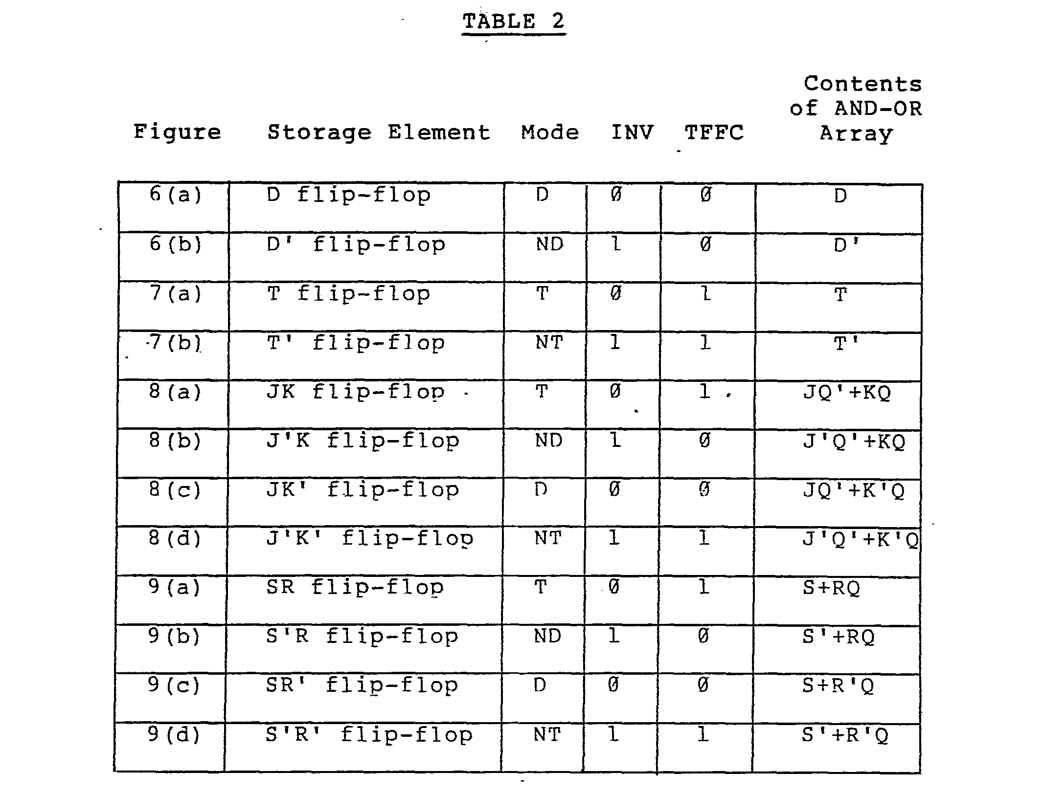
- the storage element of the present invention can be operated in four modes; namely, the D mode, the inverted D (ND) mode, the T mode, the inverted T (NT) mode. These modes are selected by appropriate choice of the inputs TFFC and INV. Once a particular mode is selected, the next state "Q+" can be predicted for any particular input (from the OR-array) and output Q.
- Figs. 6-9 illustrate various storage device types that may be emulated by the present invention and are further explained below.
- a schematic implementation of a programmable logic array including a storage element and associated feedback connections in accordance with the present invention.
- the array includes a collection of input circuits shown generally at 60 with each input having a buffer 61 with inverting and non-inverting outputs routed to a standard programmable AND array 62.
- One such array is shown in U.S. Patent Application Serial No. 607,018 filed May 3, 1984 and assigned to the assignee of the present invention.
- the outputs generated by the programmable AND array 62 are in turn input to an OR array 64 which may be either fixed or programmable as to function.
- the output of OR array 64 acts as one of four inputs to a programmable storage element 66 comprised of circuitry as shown in Fig. 4 (or alternatively, as shown in Fig. 5).
- the line 67 of the Feedback Bus is coupled to one of the input buffers as shown at 68, the output lines 69 and 70 of which are each connected to two of the AND gate lines (inputs to OR array 64) as indicated at 71 and 72 respectively.
- storage element 66 can be caused to emulate any of the twelve different types of flip-flop configurations illustrated in Figs. 6(a)-9(d) by selection of the inputs INV and TFFC in combination with appropriate programming of the AND array 62.
- the TFFC signal input on line 28 provides the controlling input which determines whether the storage element 16 will operate as a D-type or as a T-type flip-flop of a type shown in Figs. 6(A) and 7(a).
- Table 2 when TFFC is set at 0, the multiplexer 27 outputs a signal from its Y pin which causes the storag E element 16 to function as a D-type flip-flop.
- multiplexer 2 outputs a signal from its Y pin which causes stor age element 16 to function as a T-type flip-flop.
- the INV signal o line 22 which is passed to multiplexer 27 vi exclusive-OR gate 20 causes inversion of the out put on line 29 if it is set to 1 and leaves the outpt on line 29 uninverted if it is set to 0.
- the OR array or, as illustrated in Fig. 10, its input device, i.e., the AND array, collectively referred to hereinafter as the "AND-OR array" must be designed or programmed to function as a non-inverted D expression to emulate a non-inverted D-type flip-flop, as an inverted D expression to emulate an inverted D-type flip-flop and as the respective non-inverted and inverted T expressions to emulate, respectively, a non-inverted T-type flip-flop and an inverted T-type flip-flop.
- the first set of equations defining JK inputs requires three p-terms (2 for the J input and one for the K input) and the resulting T equation also has three p-terms. This establishes that a T-type flip-flop can efficiently emulate a JK-type flip-flop. (In fact, it can be demonstrated that if the J expression has n p-terms and the K expression has m p-terms, the resulting T expression will always have m + n p-terms.)
- Fig. 10 and with reference to Table 1, it can be seen that, in operation, the present invention will efficiently emulate a JK-type flip-flop of the types shown in Figs. 8(a), 8(b), 8(c) and 8 - (d) when the INV and TFFC signals are set ap- propri ately and AND-OR array is programmed correctly.
- the INV signal is set to zero
- the TFFC signal is set to one
- the AND-OR array is programmed as JQ' + KQ.
- Other emulations of JK-type flip-flops are implemented similarly and in accordance with Fig. 10 and Table 2.
- K is an expression which can be expressed using fewer p-terms in its inverted form.
- J and K terms are as follows: and five p-terms are required in the circuit. But if K can be exnressed in inverted form as the K is reduced to 1 p-term and the total requirement to three p-terms.
- the final resulting equation has three p-terms, which means that this emulation efficiently emulates a JK-type flip-flop with an inverted K input.
- This emulation results in a storage device such as that shown in Fig. 8(c). It requires only (see Table 2) that the INV and TFFC signals be cleared to zero and that the AND-OR array be programmed to JQ' + K'Q.
- Fig. 5 presents an alternate means of embodying the same logic and design features, emulation patterns and operational methods described above relative to Fig. 4.
- the major difference between the two implementations is that the multiplexer 27 in Fig. 4, the preferred embodiment, is replaced in Fig. 5 by an exclusive-NOR gate 89 and a NAND gate 47.
- these two gates may both be replaced by non-inverting gates (exclusive-OR and AND gates) and the operation of the circuit will remain identical.
- Fig. 10 One possible implementation of the present invention which takes advantage of other recent developments in programmable logic circuit design is that shown in Fig. 10 wherein the programmable storage element 66 receives one of its three significant inputs from an OR array 64 that may be eithei a fixed OR array or a programmable OR array. lr either case, the OR array 64 is connected to programmable AND array 62 so that the outputs o the AND array become the inputs to the OR array.
- OR array 64 is connected to programmable AND array 62 so that the outputs o the AND array become the inputs to the OR array
Abstract
Description
- The present invention relates generally to programmable logic array devices, and more specifically, to logic storage element architecture which permits the selective implementation of a number of different types of logic storage functions from a 'storage element circuit including a basic flip-flop element.
- Programmable logic arrays and similar circuit elements such as programmable array logic devices have been in existence for many years. For the most part, these devices are built using an architecture which consists of an AND array in combination with an OR-array. This combined array is in turn connected to an arbitrary number of storage elements, usually consisting of D-type flip-flops or, less frequently, JK-type flip-flops, with the outputs of these flip-flops being fed back to the . input array. The output pins of such devices may be connected to either or both of the. storage elements and the array. Such architecture, which is the design most commonly found in user-programmable logic devices of the type including the present invention, permits the relatively straightforward implementation of synchronous state machines, including counters and certain types of controllers.
- Two main implementations of this type of architecture have appeared in recent years. The first involves the use of a D-type flip-flop whose inputs consist of an input from the OR array and a clock pulse, with both of these inputs being connected directly to the flip-flop itself. Such design has been improved upon a routing of the signal from the OR array into an exclusive-OR gate which has an invert signal as its second input. This exclusive-OR gate's output is then routed to the D input of a D-type flip-flop and the clock pulse provides the second input. In both architectures, the output of the flip-flop is normally routed both to the output pads of the device itself and to a feedback bus which reconnects it to the AND array.
- The first design mentioned above, involving the direct connection of the input signal from the OR array into the flip-flop, has an important and troublesome restriction; namely, the logical expressions which form the input to such devices must be represented in the "sum-of-products" form so that they can be implemented in the AND-OR array. This requirement results in highly inefficient representations of some logical expressions, with the attendant problem of a proliferation of signal lines in the AND array. For example, if the flip-flop in question were to be logically driven by the equation:


- This proliferation of AND array signals becomes quite problematic when some classes of expression are required as inputs to the flip-flop. For example, if the input desired is represented by the equation:

- the expanded equation using the sum-of-products method produces 27 product terms, meaning thai 27 lines will be required in the AND array; ar inefficiently high number for a single input factor, The 27 product terms for the above equation ir sum-of-products equivalent form are:


- Some manufacturers have overcome this limi tation of AND-OR arrays by introducing program mable inverters between the OR array and thE storage element. In such embodiments, each prog rammable inverter is in turn composed of a exclusive-OR gate and an inversion control inpu supplied by a programmable fuse, or a bit from a EPROM, EEPROM, RAM or other logic-level stor age device. As a result of the use of such program mable inverters, complex logic expressions whic would otherwise generate an unacceptably large number of product terms ("p-terms") in the sum-of-products method described earlier, generate a manageable number when they are inverted. For example, the equation above, which generated 27 p-terms in its uninverted form, generates only three p-terms when inverted; namely,

- Clearly, this approach represents a significant improvement over the older methods of programmable logic device architecture. There remain, however, certain types of expressions which will require a large number of p-terms regardless of whether they are expressed in non-inverted or inverted form. A classic example-of such an expression is one widely used in defining synchronous binary counter circuits; i.e.,


- Obviously, such equations are not implemented more efficiently using the programmable inverter approach to programmable logic architecture described above.
- It is therefore an object of the present invention to provide an improved method and apparatus by which the results of certain classes of complex logic expressions may be implemented in conjunction with and applied as inputs to flip-flop circuits, either along or in combination with associated AND-OR arrays, to emulate other types of flip-flop circuits.
- Another object of the present invention is to provide a novel logic storage element which can be used to emulate flip-flop functions of the JK, RS, D or T types.
- It is a further object of the present invention to provide an improved programmable logic device including a basic flip-flop element which may be selectively caused to emulate a JK-type, RS-type, D-type or T-type logic storage device, including or inhibiting inversion on any or both inputs to the two-input type flip-flops or to the single input on a one-input type flip-flop.
- Briefly, a preferred embodiment of a storage element in accordance with the invention includes a flip-flop device and a complex logic circuit interconnected in such a way that the output of the complex logic circuit is an input to the flip-flop. A Toggle Flip-Flop Control (TFFC), an invert control - (INV) signal and a clock (CLK) signal are also inputs to the complex logic circuit. The output of the flip-flop connects to an output pad, an internal direct feedback line which is one of the means by which the flip-flop is connected to the complex logic circuit, and an external feedback bus which leads back to an associated AND-OR array. The input to the complex logic circuit is generated by the standard AND-OR array which is programmable to some degree.
- It is an advantage of the present invention that it provides a way for programmable logic circuit designers to efficiently emulate complex flip-flop logic components using programmable and less extensive and expensive component parts than would be required using conventional design methods.
- It is another advantage of the present invention that it enables implementation of a large class of complex logic expressions which would not otherwise be implementable in flip-flop circuits to be so implemented.
- It is a further advantage of the present invention that it permits such programmable logic circuits to be interfaced to OR arrays which are in turn either fixed in nature or programmable in function and which are connected to one or more programmable AND arrays, thus permitting a great deal of design flexibility in the process of implementing systems incorporating such programmable logic.
- These and other objects and advantages of the present invention will no doubt become apparant to those skilled in the art after having read the following detailed description of the preferred embodiments which are contained in and illustrated by the various drawing figures.
-
- Fig. 1 is a generalized block diagram of prior art programmable logic device including storage elements;
- Fig. 2 is a schematic diagram of a typical prior art storage element;
- Fig. 3 is a schematic diagram of a prior art D-type flip-flop storage element which incorporates a programmable inverter;
- Fig. 4 is a schematic diagram showing an improved storage element in accordance with the present invention;
- Fig. 5 is a schematic diagram showing an alternative embodiment of a storage element in accordance with the present invention;
- Figs. 6(a) and 6(b) are schematic diagrams of D-type flip-flop storage elements;
- Figs. 7(a) and 7(b) are schematic diagrams of T-type, or Toggle, flip-flop storage elements;
- Figs. 8(a) = 8(d) are schematic diagrams of JK-type flip-flop storage elements;
- Figs. 9(a) -9(b) are schematic diagrams of SR-type flip-flop storage elements; and
- Fig. 10 is a schematic drawing representing one possible implementation of a programmable logic device incorporating the present invention.
- Referring to Fig. 1 of the drawing, a prior art
programmable logic device 10 is shown to consist of three basic elements depicted by theblocks array 2 which in turn produces one or more signals to be passed via a product term bus 3 to the OR array 4 which may be either fixed or programmable. OR array 4 in turn generates one or more signals to be transmitted via thesum term bus 5 to one ormore storage elements 6 of the device. In response to clock signals (CLK) input at 11, the output ofstorage elements 6 are fed to the output pads of the device oversignal lines 7 and back to the inputs of the programmable AND array viaFeedback Bus 8. - Referring to Fig. 2, as one prior art example of a
storage element 6, a lead 5' from the sum term bus is shown connected to the flip-flop device itself, here depicted as a D-type flip-flop D-FF, but capable of being any type of flip-flop. A clock input (CLK) lead 11' provides the additional input to the flip-flop, the output Q of which is tied to the device output pads (not shown) over a line T and to the Feedback Bus over another line 8'. This is obviously the simplest embodiment used. - In Fig. 3, another prior art implementation of a storage element is shown at 6", this implementation being somewhat programmable via an invert control input on line 12 which serves as one of two inputs to an exclusive-
OR gate 13. The invert control signal (INV) is combined logically with the input on aline 5" of the sum term bus from the OR array to produce an output on thelogic line 14 which is routed to one input of the D flip-flop D-FF. The clock pulse signal input online 11" provides the second input to thestorage device 6". The output of thestorage device 6" is routed to the device output pads (not shown) over asignal line 7" and to the Feedback Bus over anotherline 8". - A first embodiment of a
storage element 16 in accordance with the present invention is shown in Fig. 4 of the drawing and includes a programmablecontrol logic circuit 18 in combination with a D flip-flop D-FF. The device includes an exclusive-OR gate 20 which receives a data signal from the OR-array at its input 21 and an invert control signal - (INV) at itsinput 22. A second exclusive-OR gate 23 accepts as inputs a feedback signal on line 24 and a split of the signal developed online 25 by the exclusive-OR gate 20.Gate 23 produces an output online 26 which provides one of three inputs to amultiplexer device 27. The other inputs to themultiplexer 27 includes the output fumished by the first exclusive-OR device 20 as a signal inline 25, and a Toggle Flip-Flop Control (TFFC) signal input online 28. Themultiplexer 27 in turn produces a signal inline 29 which is tied to the D input of the flip-flop D-FF. A clock signal (CLK) is input to D-FF at 30. Note that the output of flip-flop D-FF is connected to output pads via line 31, to thedevice feedback bus 8 by thelines 32, and to the input 24 ofgate 23 by aninternal feedback line 33, Operation of this embodiment will be describec below. - Fig. 5 illustrates a
storage device 36 including an alternative embodiment of the present inventior utilizing a different form of programmablecontro logic circuit 38 in combination with a D flip-flop D FF. In thecirucit 38, an exclusive NORgate 39 accepts the invert signal (INV) inputs on line 40 a one of its inputs and produces a signal on line 4' which acts as one input to an exclusive-OR gat E 42, the other input togate 42 being online 43 fron the OR array. The exclusive-OR gate 42 in tun produces a combined logic signal online 44 whicl serves as one input to the flip-flop D-FF, the othe input being the clock signal input online 45. Th output of flip-flop D-FF is fed back to the circuit 3: vialine 46 to one input of aNAND gate 47. Thi NAND gate, in turn, combines the feedback sign: inline 46 with a TFFC signal input on line 48 t produce an output signal online 49 which become the second input to the exclusive-NORgate 39 The output of D-FF is also fed to output pads (nc shown) via line 50 and to the device feedback bu via line 51. - Whereas the structure of two particular embodiments of the storage elements of the present invention have been described with reference to Figs. 4 and 5, a more general statement of the invention is given by the following Table 1, a so called "next state diagram" in which the sixteen possible combinations of storage element parameters are set forth. Any combination of logic components which can satisfy these requirements is deemed to be within the scope of the present invention. To facilitate understanding of the table, a simplified single block diagram is also set forth.

- As indicated by Table 1, the storage element of the present invention can be operated in four modes; namely, the D mode, the inverted D (ND) mode, the T mode, the inverted T (NT) mode. These modes are selected by appropriate choice of the inputs TFFC and INV. Once a particular mode is selected, the next state "Q+" can be predicted for any particular input (from the OR-array) and output Q.
- Figs. 6-9 illustrate various storage device types that may be emulated by the present invention and are further explained below.
- In Fig. 10, a schematic implementation of a programmable logic array is shown including a storage element and associated feedback connections in accordance with the present invention. As depicted, the array includes a collection of input circuits shown generally at 60 with each input having a
buffer 61 with inverting and non-inverting outputs routed to a standard programmable ANDarray 62. One such array is shown in U.S. Patent Application Serial No. 607,018 filed May 3, 1984 and assigned to the assignee of the present invention. The outputs generated by the programmable ANDarray 62 are in turn input to an OR array 64 which may be either fixed or programmable as to function. The output of OR array 64 acts as one of four inputs to aprogrammable storage element 66 comprised of circuitry as shown in Fig. 4 (or alternatively, as shown in Fig. 5). - Note that the
line 67 of the Feedback Bus is coupled to one of the input buffers as shown at 68, theoutput lines storage element 66 can be caused to emulate any of the twelve different types of flip-flop configurations illustrated in Figs. 6(a)-9(d) by selection of the inputs INV and TFFC in combination with appropriate programming of the ANDarray 62. - During the following dicussion of operation of the present invention, reference will be made to the following Table 2 which provides the definitions for the three main inputs -INV, TFFC and the contents of the AND-Or array (62, 64) needed by the present invention in order to emulate the various types of storage elements shown in Figs 6(a)-9(d). This is because the functional operation of the present invention can only be described in terms of its emulation of the various standard kinds of flip-flop storage elements shown in those figures. The statements listed under the heading "Contents of AND-OR Array" are the Boolean expressions to which the AND array must be programmed in order that the desired emulation may be accomplished.
- Referring now back to Fig. 4 of the drawing, it will be appreciated that the TFFC signal input on
line 28 provides the controlling input which determines whether thestorage element 16 will operate as a D-type or as a T-type flip-flop of a type shown in Figs. 6(A) and 7(a). As can be seen in Table 2, when TFFC is set at 0, themultiplexer 27 outputs a signal from its Y pin which causes the storagE element 16 to function as a D-type flip-flop. On th other hand, when TFFC is set to 1,multiplexer 2 outputs a signal from its Y pin which causesstor age element 16 to function as a T-type flip-flop. - In both emulation situations, the INV
signal o line 22 which is passed to multiplexer 27 vi exclusive-OR gate 20 causes inversion of the out put online 29 if it is set to 1 and leaves the outpt online 29 uninverted if it is set to 0. - The OR array or, as illustrated in Fig. 10, its input device, i.e., the AND array, collectively referred to hereinafter as the "AND-OR array" must be designed or programmed to function as a non-inverted D expression to emulate a non-inverted D-type flip-flop, as an inverted D expression to emulate an inverted D-type flip-flop and as the respective non-inverted and inverted T expressions to emulate, respectively, a non-inverted T-type flip-flop and an inverted T-type flip-flop.
- Thus by manipulating the levels of the INV and TFFC signals and programming the OR array or its input correctly as shown in Fig. 10, (and as set forth in Tables 1 and 2), one can successfully cause the storage element of the present invention to function as any of the four common types of storage devices.
- Emulation of JK Flip-Flops.
- In the ensuing discussion of the operation of the present invention in the emulation of a JK-type flip-flop, it is important to remember that it is possible to add factors to a p-term in an AND array at no additional cost of interconnection or efficiency, and that if a given signal is available as an input to a given AND array, then its inverse is available as well, this is due to the fact that inverse signals are easily generated for AND arrays by well-established conventional methods.
- Programming the equation:


- If a requirement exists to design a JK-type flip-flop which has the following expression associated with its inputs:


- As can be readily seen from the above, the first set of equations defining JK inputs requires three p-terms (2 for the J input and one for the K input) and the resulting T equation also has three p-terms. This establishes that a T-type flip-flop can efficiently emulate a JK-type flip-flop. (In fact, it can be demonstrated that if the J expression has n p-terms and the K expression has m p-terms, the resulting T expression will always have m + n p-terms.)
- Turning to Fig. 10, and with reference to Table 1, it can be seen that, in operation, the present invention will efficiently emulate a JK-type flip-flop of the types shown in Figs. 8(a), 8(b), 8(c) and 8 - (d) when the INV and TFFC signals are set ap- propri ately and AND-OR array is programmed correctly. For example, to emulate a non-inverted JK-type flip-flop, the INV signal is set to zero, the TFFC signal is set to one and the AND-OR array is programmed as JQ' + KQ. Other emulations of JK-type flip-flops are implemented similarly and in accordance with Fig. 10 and Table 2.
- Interestingly, it is possible with the present invention to achieve even greater efficiency of emulation of a JK-type flip-flop where K is an expression which can be expressed using fewer p-terms in its inverted form. For example, if J and K terms are as follows:


- The equation which permits a D-type flip-flop to emulate a JK-type flip-flop has K expressed in its inverted form, as shown:


- The final resulting equation has three p-terms, which means that this emulation efficiently emulates a JK-type flip-flop with an inverted K input. This emulation results in a storage device such as that shown in Fig. 8(c). It requires only (see Table 2) that the INV and TFFC signals be cleared to zero and that the AND-OR array be programmed to JQ' + K'Q.
- The emulation of SR-Type flip-flops using the present invention can be easily deduced from an examination of Figs. 9(a), 9(b), 9(c) and 9(d),along with Table 2. Since the logic sequences and formulas involved here are virtually identical to those described above in discussing the emulation of JK-type flip-flops, and since the underlying logic formulas are well known in the art, a detailed discussion of this implementation and emulation is not deemed necessary here.
- As explained above, Fig. 5 presents an alternate means of embodying the same logic and design features, emulation patterns and operational methods described above relative to Fig. 4. The major difference between the two implementations is that the
multiplexer 27 in Fig. 4, the preferred embodiment, is replaced in Fig. 5 by an exclusive-NOR gate 89 and aNAND gate 47. In fact, these two gates may both be replaced by non-inverting gates (exclusive-OR and AND gates) and the operation of the circuit will remain identical. - The setting of the INV and TFFC signals, and the programming of the AND array, are identical for the circuit shown in Fig. 5 as for that shown in Fig. 4; therefore, the values of Table 2 remain valid for the alternate embodiment of the present invention shown in Fig. 5.
- One possible implementation of the present invention which takes advantage of other recent developments in programmable logic circuit design is that shown in Fig. 10 wherein the
programmable storage element 66 receives one of its three significant inputs from an OR array 64 that may be eithei a fixed OR array or a programmable OR array. lr either case, the OR array 64 is connected to programmable ANDarray 62 so that the outputs o the AND array become the inputs to the OR array This method of providing flexibility in program mable logic circuit designs is further explained anc taught in detail in the aforementioned U.S. Paten Application Serial No. 607,018. - Although the present invention has been de scribed in terms of specific embodiments, it i: anticipated that alterations and modifications there of will no doubt become apparent to those skillec in the art. It is therefore intended that the foliowinc claims be interpreted as covering all such alter ations and modifications as fall within the true spiri and scope of the invention.
- The features disclosed in the foregoing de scription, in the following claims and/or in the ac companying drawings may, both separately and ii any combination thereof, be material for realising the invention in diverse forms thereof.
Claims (10)
Priority Applications (1)
| Application Number | Priority Date | Filing Date | Title |
|---|---|---|---|
| AT86302681T ATE65652T1 (en) | 1985-04-12 | 1986-04-10 | PROGRAMMABLE LOGICAL MEMORY ELEMENT FOR PROGRAMMABLE LOGICAL DEVICES. |
Applications Claiming Priority (2)
| Application Number | Priority Date | Filing Date | Title |
|---|---|---|---|
| US722684 | 1985-04-12 | ||
| US06/722,684 US4677318A (en) | 1985-04-12 | 1985-04-12 | Programmable logic storage element for programmable logic devices |
Publications (3)
| Publication Number | Publication Date |
|---|---|
| EP0198677A2 true EP0198677A2 (en) | 1986-10-22 |
| EP0198677A3 EP0198677A3 (en) | 1987-12-09 |
| EP0198677B1 EP0198677B1 (en) | 1991-07-24 |
Family
ID=24902922
Family Applications (1)
| Application Number | Title | Priority Date | Filing Date |
|---|---|---|---|
| EP86302681A Expired - Lifetime EP0198677B1 (en) | 1985-04-12 | 1986-04-10 | Programmable logic storage element for programmable logic devices |
Country Status (5)
| Country | Link |
|---|---|
| US (1) | US4677318A (en) |
| EP (1) | EP0198677B1 (en) |
| JP (1) | JPS61292414A (en) |
| AT (1) | ATE65652T1 (en) |
| DE (1) | DE3680373D1 (en) |
Cited By (4)
| Publication number | Priority date | Publication date | Assignee | Title |
|---|---|---|---|---|
| EP0350141A2 (en) * | 1988-05-05 | 1990-01-10 | Altera Corporation | Multifunction flip-flop-type circuit |
| US4933577A (en) * | 1985-03-22 | 1990-06-12 | Advanced Micro Devices, Inc. | Output circuit for a programmable logic array |
| EP0406786A1 (en) * | 1989-07-04 | 1991-01-09 | ALCATEL ITALIA S.p.A. | Device for transforming a type "D" flip-flop into a flip-flop called type "B" able to sample data both on leading and trailing edges of the clock signal |
| EP0541840A1 (en) * | 1991-11-11 | 1993-05-19 | Hewlett-Packard GmbH | Formatter circuit |
Families Citing this family (138)
| Publication number | Priority date | Publication date | Assignee | Title |
|---|---|---|---|---|
| US5225719A (en) * | 1985-03-29 | 1993-07-06 | Advanced Micro Devices, Inc. | Family of multiple segmented programmable logic blocks interconnected by a high speed centralized switch matrix |
| US4876640A (en) * | 1986-02-07 | 1989-10-24 | Advanced Micro Devices, Inc. | Logic controller having programmable logic "and" array using a programmable gray-code counter |
| US4789951A (en) * | 1986-05-16 | 1988-12-06 | Advanced Micro Devices, Inc. | Programmable array logic cell |
| US5367208A (en) | 1986-09-19 | 1994-11-22 | Actel Corporation | Reconfigurable programmable interconnect architecture |
| US5477165A (en) * | 1986-09-19 | 1995-12-19 | Actel Corporation | Programmable logic module and architecture for field programmable gate array device |
| US5451887A (en) * | 1986-09-19 | 1995-09-19 | Actel Corporation | Programmable logic module and architecture for field programmable gate array device |
| US4831573A (en) * | 1987-03-06 | 1989-05-16 | Altera Corporation | Programmable integrated circuit micro-sequencer device |
| US4783606A (en) * | 1987-04-14 | 1988-11-08 | Erich Goetting | Programming circuit for programmable logic array I/O cell |
| US4871930A (en) * | 1988-05-05 | 1989-10-03 | Altera Corporation | Programmable logic device with array blocks connected via programmable interconnect |
| US4912342A (en) * | 1988-05-05 | 1990-03-27 | Altera Corporation | Programmable logic device with array blocks with programmable clocking |
| US4903223A (en) * | 1988-05-05 | 1990-02-20 | Altera Corporation | Programmable logic device with programmable word line connections |
| US4899070A (en) * | 1988-07-13 | 1990-02-06 | Altera Corporation | Bit line sense amplifier for programmable logic devices |
| US4899067A (en) * | 1988-07-22 | 1990-02-06 | Altera Corporation | Programmable logic devices with spare circuits for use in replacing defective circuits |
| US4914322A (en) * | 1988-12-16 | 1990-04-03 | Advanced Micro Devices, Inc. | Polarity option control logic for use with a register of a programmable logic array macrocell |
| US4942319A (en) * | 1989-01-19 | 1990-07-17 | National Semiconductor Corp. | Multiple page programmable logic architecture |
| US5343406A (en) * | 1989-07-28 | 1994-08-30 | Xilinx, Inc. | Distributed memory architecture for a configurable logic array and method for using distributed memory |
| US5233539A (en) * | 1989-08-15 | 1993-08-03 | Advanced Micro Devices, Inc. | Programmable gate array with improved interconnect structure, input/output structure and configurable logic block |
| US5212652A (en) * | 1989-08-15 | 1993-05-18 | Advanced Micro Devices, Inc. | Programmable gate array with improved interconnect structure |
| US5644496A (en) * | 1989-08-15 | 1997-07-01 | Advanced Micro Devices, Inc. | Programmable logic device with internal time-constant multiplexing of signals from external interconnect buses |
| US5260881A (en) * | 1989-10-30 | 1993-11-09 | Advanced Micro Devices, Inc. | Programmable gate array with improved configurable logic block |
| US5028821A (en) * | 1990-03-01 | 1991-07-02 | Plus Logic, Inc. | Programmable logic device with programmable inverters at input/output pads |
| US5043606A (en) * | 1990-03-30 | 1991-08-27 | Seagate Technology, Inc. | Apparatus and method for programmably controlling the polarity of an I/O signal of a magnetic disk drive |
| US5198705A (en) * | 1990-05-11 | 1993-03-30 | Actel Corporation | Logic module with configurable combinational and sequential blocks |
| US6759870B2 (en) | 1991-09-03 | 2004-07-06 | Altera Corporation | Programmable logic array integrated circuits |
| US5260610A (en) * | 1991-09-03 | 1993-11-09 | Altera Corporation | Programmable logic element interconnections for programmable logic array integrated circuits |
| DE69225564T2 (en) * | 1991-11-29 | 1998-11-26 | Philips Electronics Nv | Magnetic resonance arrangement |
| US5434514A (en) * | 1992-11-19 | 1995-07-18 | Altera Corporation | Programmable logic devices with spare circuits for replacement of defects |
| US5483178A (en) * | 1993-03-29 | 1996-01-09 | Altera Corporation | Programmable logic device with logic block outputs coupled to adjacent logic block output multiplexers |
| US5399922A (en) * | 1993-07-02 | 1995-03-21 | Altera Corporation | Macrocell comprised of two look-up tables and two flip-flops |
| US5581200A (en) * | 1994-03-04 | 1996-12-03 | Gudger; Keith H. | Stored and combinational logic function generator without dedicated storage elements |
| US6294928B1 (en) | 1996-04-05 | 2001-09-25 | Altera Corporation | Programmable logic device with highly routable interconnect |
| US6181162B1 (en) | 1994-04-10 | 2001-01-30 | Altera Corporation | Programmable logic device with highly routable interconnect |
| USRE38651E1 (en) * | 1994-05-18 | 2004-11-09 | Altera Corporation | Variable depth and width memory device |
| US5689195A (en) | 1995-05-17 | 1997-11-18 | Altera Corporation | Programmable logic array integrated circuit devices |
| FI98017C (en) * | 1994-06-03 | 1997-03-25 | Nokia Telecommunications Oy | chipset |
| US5815726A (en) * | 1994-11-04 | 1998-09-29 | Altera Corporation | Coarse-grained look-up table architecture |
| US5898318A (en) * | 1994-11-04 | 1999-04-27 | Altera Corporation | Programmable logic array integrated circuits with enhanced cascade |
| US5525917A (en) * | 1994-12-16 | 1996-06-11 | Altera Corporation | Sense amplifier with feedback and stabilization |
| US5850365A (en) * | 1994-12-16 | 1998-12-15 | Altera Corporation | Sense amplifier with individually optimized high and low power modes |
| US5537057A (en) * | 1995-02-14 | 1996-07-16 | Altera Corporation | Programmable logic array device with grouped logic regions and three types of conductors |
| US5909126A (en) | 1995-05-17 | 1999-06-01 | Altera Corporation | Programmable logic array integrated circuit devices with interleaved logic array blocks |
| US5963049A (en) | 1995-05-17 | 1999-10-05 | Altera Corporation | Programmable logic array integrated circuit architectures |
| US5543732A (en) * | 1995-05-17 | 1996-08-06 | Altera Corporation | Programmable logic array devices with interconnect lines of various lengths |
| US5900743A (en) | 1995-05-17 | 1999-05-04 | Altera Corporation | Programmable logic array devices with interconnect lines of various lengths |
| US5543730A (en) | 1995-05-17 | 1996-08-06 | Altera Corporation | Techniques for programming programmable logic array devices |
| GB2300946B (en) * | 1995-05-17 | 1999-10-20 | Altera Corp | Tri-statable input/output circuitry for programmable logic |
| US5592106A (en) * | 1995-05-17 | 1997-01-07 | Altera Corporation | Programmable logic array integrated circuits with interconnection conductors of overlapping extent |
| US5614840A (en) * | 1995-05-17 | 1997-03-25 | Altera Corporation | Programmable logic array integrated circuits with segmented, selectively connectable, long interconnection conductors |
| US5541530A (en) * | 1995-05-17 | 1996-07-30 | Altera Corporation | Programmable logic array integrated circuits with blocks of logic regions grouped into super-blocks |
| US6028446A (en) * | 1995-06-06 | 2000-02-22 | Advanced Micro Devices, Inc. | Flexible synchronous and asynchronous circuits for a very high density programmable logic device |
| US5659717A (en) * | 1995-07-31 | 1997-08-19 | Altera Corporation | Methods for partitioning circuits in order to allocate elements among multiple circuit groups |
| US5581501A (en) * | 1995-08-17 | 1996-12-03 | Altera Corporation | Nonvolatile SRAM cells and cell arrays |
| US5565793A (en) * | 1995-08-22 | 1996-10-15 | Altera Corporation | Programmable logic array integrated circuit devices with regions of enhanced interconnectivity |
| US5764080A (en) * | 1995-08-24 | 1998-06-09 | Altera Corporation | Input/output interface circuitry for programmable logic array integrated circuit devices |
| US5631576A (en) * | 1995-09-01 | 1997-05-20 | Altera Corporation | Programmable logic array integrated circuit devices with flexible carry chains |
| US5821773A (en) * | 1995-09-06 | 1998-10-13 | Altera Corporation | Look-up table based logic element with complete permutability of the inputs to the secondary signals |
| US5729495A (en) * | 1995-09-29 | 1998-03-17 | Altera Corporation | Dynamic nonvolatile memory cell |
| US5970255A (en) | 1995-10-16 | 1999-10-19 | Altera Corporation | System for coupling programmable logic device to external circuitry which selects a logic standard and uses buffers to modify output and input signals accordingly |
| US5744991A (en) * | 1995-10-16 | 1998-04-28 | Altera Corporation | System for distributing clocks using a delay lock loop in a programmable logic circuit |
| US5670895A (en) * | 1995-10-19 | 1997-09-23 | Altera Corporation | Routing connections for programmable logic array integrated circuits |
| US5592102A (en) * | 1995-10-19 | 1997-01-07 | Altera Corporation | Means and apparatus to minimize the effects of silicon processing defects in programmable logic devices |
| US5793246A (en) * | 1995-11-08 | 1998-08-11 | Altera Corporation | High voltage pump scheme incorporating an overlapping clock |
| US5684744A (en) * | 1995-12-11 | 1997-11-04 | Hewlett-Packard Company | Configurable multifunction flip-flop |
| US5672985A (en) * | 1995-12-18 | 1997-09-30 | Altera Corporation | Programmable logic array integrated circuits with carry and/or cascade rings |
| US5767734A (en) * | 1995-12-21 | 1998-06-16 | Altera Corporation | High-voltage pump with initiation scheme |
| US6882177B1 (en) | 1996-01-10 | 2005-04-19 | Altera Corporation | Tristate structures for programmable logic devices |
| US5894228A (en) * | 1996-01-10 | 1999-04-13 | Altera Corporation | Tristate structures for programmable logic devices |
| US5691653A (en) * | 1996-01-16 | 1997-11-25 | Altera Corporation | Product term based programmable logic array devices with reduced control memory requirements |
| US5744980A (en) * | 1996-02-16 | 1998-04-28 | Actel Corporation | Flexible, high-performance static RAM architecture for field-programmable gate arrays |
| US5787009A (en) * | 1996-02-20 | 1998-07-28 | Altera Corporation | Methods for allocating circuit design portions among physical circuit portions |
| US5768372A (en) * | 1996-03-13 | 1998-06-16 | Altera Corporation | Method and apparatus for securing programming data of a programmable logic device |
| US6005806A (en) * | 1996-03-14 | 1999-12-21 | Altera Corporation | Nonvolatile configuration cells and cell arrays |
| US5694058A (en) * | 1996-03-20 | 1997-12-02 | Altera Corporation | Programmable logic array integrated circuits with improved interconnection conductor utilization |
| US5835998A (en) * | 1996-04-04 | 1998-11-10 | Altera Corporation | Logic cell for programmable logic devices |
| US5872463A (en) * | 1996-04-04 | 1999-02-16 | Altera Corporation | Routing in programmable logic devices using shared distributed programmable logic connectors |
| US5869979A (en) * | 1996-04-05 | 1999-02-09 | Altera Corporation | Technique for preconditioning I/Os during reconfiguration |
| US6107822A (en) | 1996-04-09 | 2000-08-22 | Altera Corporation | Logic element for a programmable logic integrated circuit |
| US5986465A (en) * | 1996-04-09 | 1999-11-16 | Altera Corporation | Programmable logic integrated circuit architecture incorporating a global shareable expander |
| US6034540A (en) | 1997-04-08 | 2000-03-07 | Altera Corporation | Programmable logic integrated circuit architecture incorporating a lonely register |
| US5939790A (en) * | 1996-04-09 | 1999-08-17 | Altera Corporation | Integrated circuit pad structures |
| US5949710A (en) * | 1996-04-10 | 1999-09-07 | Altera Corporation | Programmable interconnect junction |
| US5998295A (en) * | 1996-04-10 | 1999-12-07 | Altera Corporation | Method of forming a rough region on a substrate |
| US5977791A (en) | 1996-04-15 | 1999-11-02 | Altera Corporation | Embedded memory block with FIFO mode for programmable logic device |
| US6147511A (en) | 1996-05-28 | 2000-11-14 | Altera Corporation | Overvoltage-tolerant interface for integrated circuits |
| US6025737A (en) * | 1996-11-27 | 2000-02-15 | Altera Corporation | Circuitry for a low internal voltage integrated circuit |
| US6384630B2 (en) | 1996-06-05 | 2002-05-07 | Altera Corporation | Techniques for programming programmable logic array devices |
| US5715197A (en) | 1996-07-29 | 1998-02-03 | Xilinx, Inc. | Multiport RAM with programmable data port configuration |
| US5959891A (en) * | 1996-08-16 | 1999-09-28 | Altera Corporation | Evaluation of memory cell characteristics |
| US5771264A (en) * | 1996-08-29 | 1998-06-23 | Altera Corporation | Digital delay lock loop for clock signal frequency multiplication |
| US6236597B1 (en) | 1996-09-16 | 2001-05-22 | Altera Corporation | Nonvolatile memory cell with multiple gate oxide thicknesses |
| US6018476A (en) * | 1996-09-16 | 2000-01-25 | Altera Corporation | Nonvolatile configuration cells and cell arrays |
| US5880597A (en) * | 1996-09-18 | 1999-03-09 | Altera Corporation | Interleaved interconnect for programmable logic array devices |
| US5844854A (en) * | 1996-09-18 | 1998-12-01 | Altera Corporation | Programmable logic device with two dimensional memory addressing |
| US5914904A (en) * | 1996-10-01 | 1999-06-22 | Altera Corporation | Compact electrically erasable memory cells and arrays |
| US5999016A (en) * | 1996-10-10 | 1999-12-07 | Altera Corporation | Architectures for programmable logic devices |
| US5977793A (en) * | 1996-10-10 | 1999-11-02 | Altera Corporation | Programmable logic device with hierarchical interconnection resources |
| US6300794B1 (en) | 1996-10-10 | 2001-10-09 | Altera Corporation | Programmable logic device with hierarchical interconnection resources |
| US5942914A (en) * | 1996-10-25 | 1999-08-24 | Altera Corporation | PLD with split multiplexed inputs from global conductors |
| US5959466A (en) * | 1997-01-31 | 1999-09-28 | Actel Corporation | Field programmable gate array with mask programmed input and output buffers |
| US5936426A (en) * | 1997-02-03 | 1999-08-10 | Actel Corporation | Logic function module for field programmable array |
| US6091258A (en) * | 1997-02-05 | 2000-07-18 | Altera Corporation | Redundancy circuitry for logic circuits |
| US6034536A (en) * | 1997-02-05 | 2000-03-07 | Altera Corporation | Redundancy circuitry for logic circuits |
| US5982195A (en) * | 1997-02-20 | 1999-11-09 | Altera Corporation | Programmable logic device architectures |
| US7148722B1 (en) | 1997-02-20 | 2006-12-12 | Altera Corporation | PCI-compatible programmable logic devices |
| US6127844A (en) | 1997-02-20 | 2000-10-03 | Altera Corporation | PCI-compatible programmable logic devices |
| US5999015A (en) * | 1997-02-20 | 1999-12-07 | Altera Corporation | Logic region resources for programmable logic devices |
| US6150837A (en) * | 1997-02-28 | 2000-11-21 | Actel Corporation | Enhanced field programmable gate array |
| US6184710B1 (en) | 1997-03-20 | 2001-02-06 | Altera Corporation | Programmable logic array devices with enhanced interconnectivity between adjacent logic regions |
| JP3865789B2 (en) * | 1997-05-23 | 2007-01-10 | アルテラ コーポレイション | Redundant circuit for programmable logic device with interleaved input circuit |
| US6239612B1 (en) | 1997-08-20 | 2001-05-29 | Altera Corporation | Programmable I/O cells with multiple drivers |
| US6130555A (en) * | 1997-10-13 | 2000-10-10 | Altera Corporation | Driver circuitry for programmable logic devices |
| US6052327A (en) * | 1997-10-14 | 2000-04-18 | Altera Corporation | Dual-port programmable logic device variable depth and width memory array |
| US6084427A (en) | 1998-05-19 | 2000-07-04 | Altera Corporation | Programmable logic devices with enhanced multiplexing capabilities |
| US6191998B1 (en) | 1997-10-16 | 2001-02-20 | Altera Corporation | Programmable logic device memory array circuit having combinable single-port memory arrays |
| US6121790A (en) * | 1997-10-16 | 2000-09-19 | Altera Corporation | Programmable logic device with enhanced multiplexing capabilities in interconnect resources |
| US6107825A (en) * | 1997-10-16 | 2000-08-22 | Altera Corporation | Input/output circuitry for programmable logic devices |
| US6107824A (en) * | 1997-10-16 | 2000-08-22 | Altera Corporation | Circuitry and methods for internal interconnection of programmable logic devices |
| US6288970B1 (en) | 1997-10-16 | 2001-09-11 | Altera Corporation | Programmable logic device memory array circuit having combinable single-port memory arrays |
| US6255850B1 (en) | 1997-10-28 | 2001-07-03 | Altera Corporation | Integrated circuit with both clamp protection and high impedance protection from input overshoot |
| US6201404B1 (en) | 1998-07-14 | 2001-03-13 | Altera Corporation | Programmable logic device with redundant circuitry |
| US6184707B1 (en) | 1998-10-07 | 2001-02-06 | Altera Corporation | Look-up table based logic element with complete permutability of the inputs to the secondary signals |
| US6215326B1 (en) | 1998-11-18 | 2001-04-10 | Altera Corporation | Programmable logic device architecture with super-regions having logic regions and a memory region |
| US6507216B1 (en) | 1998-11-18 | 2003-01-14 | Altera Corporation | Efficient arrangement of interconnection resources on programmable logic devices |
| US6407576B1 (en) * | 1999-03-04 | 2002-06-18 | Altera Corporation | Interconnection and input/output resources for programmable logic integrated circuit devices |
| US7484081B1 (en) | 2000-10-10 | 2009-01-27 | Altera Corporation | Method and apparatus for protecting designs in SRAM-based programmable logic devices |
| US6466505B1 (en) | 2001-05-02 | 2002-10-15 | Cypress Semiconductor Corp. | Flexible input structure for an embedded memory |
| US6810513B1 (en) * | 2002-06-19 | 2004-10-26 | Altera Corporation | Method and apparatus of programmable interconnect array with configurable multiplexer |
| US7111110B1 (en) | 2002-12-10 | 2006-09-19 | Altera Corporation | Versatile RAM for programmable logic device |
| US8612772B1 (en) | 2004-09-10 | 2013-12-17 | Altera Corporation | Security core using soft key |
| US8566616B1 (en) | 2004-09-10 | 2013-10-22 | Altera Corporation | Method and apparatus for protecting designs in SRAM-based programmable logic devices and the like |
| US8438522B1 (en) | 2008-09-24 | 2013-05-07 | Iowa State University Research Foundation, Inc. | Logic element architecture for generic logic chains in programmable devices |
| US8661394B1 (en) | 2008-09-24 | 2014-02-25 | Iowa State University Research Foundation, Inc. | Depth-optimal mapping of logic chains in reconfigurable fabrics |
| US8736299B1 (en) | 2011-04-29 | 2014-05-27 | Altera Corporation | Setting security features of programmable logic devices |
| US8627105B2 (en) | 2011-04-29 | 2014-01-07 | Altera Corporation | Method and apparatus for securing programming data of a programmable device |
| US8719957B2 (en) | 2011-04-29 | 2014-05-06 | Altera Corporation | Systems and methods for detecting and mitigating programmable logic device tampering |
| US8461863B2 (en) | 2011-04-29 | 2013-06-11 | Altera Corporation | Method and apparatus for securing a programmable device using a kill switch |
| US9026873B2 (en) | 2013-07-23 | 2015-05-05 | Altera Coporation | Method and apparatus for securing configuration scan chains of a programmable device |
| US9584121B2 (en) * | 2015-06-10 | 2017-02-28 | Qualcomm Incorporated | Compact design of scan latch |
Citations (2)
| Publication number | Priority date | Publication date | Assignee | Title |
|---|---|---|---|---|
| US4124899A (en) * | 1977-05-23 | 1978-11-07 | Monolithic Memories, Inc. | Programmable array logic circuit |
| US4422072A (en) * | 1981-07-30 | 1983-12-20 | Signetics Corporation | Field programmable logic array circuit |
Family Cites Families (3)
| Publication number | Priority date | Publication date | Assignee | Title |
|---|---|---|---|---|
| US4034356A (en) * | 1975-12-03 | 1977-07-05 | Ibm Corporation | Reconfigurable logic array |
| US4433331A (en) * | 1981-12-14 | 1984-02-21 | Bell Telephone Laboratories, Incorporated | Programmable logic array interconnection matrix |
| US4525641A (en) * | 1982-12-10 | 1985-06-25 | International Business Machines Corporation | Flip-flop programmer using cascaded logic arrays |
-
1985
- 1985-04-12 US US06/722,684 patent/US4677318A/en not_active Expired - Lifetime
-
1986
- 1986-04-10 DE DE8686302681T patent/DE3680373D1/en not_active Expired - Lifetime
- 1986-04-10 AT AT86302681T patent/ATE65652T1/en not_active IP Right Cessation
- 1986-04-10 EP EP86302681A patent/EP0198677B1/en not_active Expired - Lifetime
- 1986-04-11 JP JP61082402A patent/JPS61292414A/en active Granted
Patent Citations (3)
| Publication number | Priority date | Publication date | Assignee | Title |
|---|---|---|---|---|
| US4124899A (en) * | 1977-05-23 | 1978-11-07 | Monolithic Memories, Inc. | Programmable array logic circuit |
| US4124899B1 (en) * | 1977-05-23 | 1987-04-28 | ||
| US4422072A (en) * | 1981-07-30 | 1983-12-20 | Signetics Corporation | Field programmable logic array circuit |
Non-Patent Citations (3)
| Title |
|---|
| ELECTRONIC DESIGN, 11th July 1985; "EPROM-based logic chip opens its gates to all flip-flop types, clocks" * |
| ELECTRONIC ENGINEERING, vol. 56, no. 687, March 1984, pages 147-150, London, GB; J. GABRIS "The evolution of programmable logic" * |
| IEE PROCEEDINGS, vol. 132, no. 2, Part I, March/April 1985, pages 73-85, Old Woking, Surrey, GB; M.J.P. BOLTON et al.: "Designing with programmable logic" * |
Cited By (7)
| Publication number | Priority date | Publication date | Assignee | Title |
|---|---|---|---|---|
| US4933577A (en) * | 1985-03-22 | 1990-06-12 | Advanced Micro Devices, Inc. | Output circuit for a programmable logic array |
| EP0350141A2 (en) * | 1988-05-05 | 1990-01-10 | Altera Corporation | Multifunction flip-flop-type circuit |
| EP0350141A3 (en) * | 1988-05-05 | 1990-10-10 | Altera Corporation | Multifunction flip-flop-type circuit |
| EP0406786A1 (en) * | 1989-07-04 | 1991-01-09 | ALCATEL ITALIA S.p.A. | Device for transforming a type "D" flip-flop into a flip-flop called type "B" able to sample data both on leading and trailing edges of the clock signal |
| US5081370A (en) * | 1989-07-04 | 1992-01-14 | Alcatel N.V. | Type "b" flip-flop |
| EP0541840A1 (en) * | 1991-11-11 | 1993-05-19 | Hewlett-Packard GmbH | Formatter circuit |
| US5293079A (en) * | 1991-11-11 | 1994-03-08 | Hewlett-Packard Company | Formatter circuit |
Also Published As
| Publication number | Publication date |
|---|---|
| US4677318A (en) | 1987-06-30 |
| EP0198677A3 (en) | 1987-12-09 |
| DE3680373D1 (en) | 1991-08-29 |
| JPH0431607B2 (en) | 1992-05-27 |
| EP0198677B1 (en) | 1991-07-24 |
| ATE65652T1 (en) | 1991-08-15 |
| JPS61292414A (en) | 1986-12-23 |
Similar Documents
| Publication | Publication Date | Title |
|---|---|---|
| EP0198677A2 (en) | Programmable logic storage element for programmable logic devices | |
| US5530378A (en) | Cross point interconnect structure with reduced area | |
| US4912345A (en) | Programmable summing functions for programmable logic devices | |
| US5136188A (en) | Input/output macrocell for programmable logic device | |
| JP3005644B2 (en) | Input circuit for programmable logic device, logic circuit for use in programmable logic device, and programmable logic device | |
| EP0372749B1 (en) | Semiconductor integrated circuit | |
| EP0456399A2 (en) | Logic module with configurable combinational and sequential blocks | |
| US20030234667A1 (en) | PLDs providing reduced delays in cascade chain circuits | |
| JPH07504797A (en) | Macrocell with cascade of logical product terms and improved use of flip-flops | |
| JPH06295233A (en) | Programmable logic apparatus and method for realizing logical function in reprogrammable logic | |
| EP0395206B1 (en) | Logic circuit and method of operating same | |
| US4835414A (en) | Flexible, reconfigurable terminal pin | |
| GB2193058A (en) | Four-state i/o control circuit | |
| US3932734A (en) | Binary parallel adder employing high speed gating circuitry | |
| US4300060A (en) | Signal programmable multiple function flip-flop | |
| GB1158134A (en) | Improved Multirank Multistage Shift Register | |
| US4701877A (en) | Highspeed parallel adder with clocked switching circuits | |
| US6353920B1 (en) | Method for implementing wide gates and tristate buffers using FPGA carry logic | |
| KR960042413A (en) | Data processing system | |
| US4644192A (en) | Programmable array logic with shared product terms and J-K registered outputs | |
| EP0130293B1 (en) | Latching circuit array of logic gates | |
| US7417455B2 (en) | Programmable function generator and method operating as combinational, sequential and routing cells | |
| US3380033A (en) | Computer apparatus | |
| McCluskey | Logical design theory of NOR gate networks with no complemented inputs | |
| EP0733285A1 (en) | Combined programmable logic array and array logic |
Legal Events
| Date | Code | Title | Description |
|---|---|---|---|
| PUAI | Public reference made under article 153(3) epc to a published international application that has entered the european phase |
Free format text: ORIGINAL CODE: 0009012 |
|
| AK | Designated contracting states |
Kind code of ref document: A2 Designated state(s): AT BE CH DE FR GB IT LI LU NL SE |
|
| PUAL | Search report despatched |
Free format text: ORIGINAL CODE: 0009013 |
|
| AK | Designated contracting states |
Kind code of ref document: A3 Designated state(s): AT BE CH DE FR GB IT LI LU NL SE |
|
| 17P | Request for examination filed |
Effective date: 19880328 |
|
| 17Q | First examination report despatched |
Effective date: 19900326 |
|
| ITF | It: translation for a ep patent filed |
Owner name: FIAMMENGHI - DOMENIGHETTI |
|
| GRAA | (expected) grant |
Free format text: ORIGINAL CODE: 0009210 |
|
| AK | Designated contracting states |
Kind code of ref document: B1 Designated state(s): AT BE CH DE FR GB IT LI LU NL SE |
|
| PG25 | Lapsed in a contracting state [announced via postgrant information from national office to epo] |
Ref country code: SE Effective date: 19910724 Ref country code: NL Effective date: 19910724 Ref country code: LI Effective date: 19910724 Ref country code: CH Effective date: 19910724 Ref country code: BE Effective date: 19910724 Ref country code: AT Effective date: 19910724 |
|
| REF | Corresponds to: |
Ref document number: 65652 Country of ref document: AT Date of ref document: 19910815 Kind code of ref document: T |
|
| REF | Corresponds to: |
Ref document number: 3680373 Country of ref document: DE Date of ref document: 19910829 |
|
| ET | Fr: translation filed | ||
| REG | Reference to a national code |
Ref country code: CH Ref legal event code: PL |
|
| NLV1 | Nl: lapsed or annulled due to failure to fulfill the requirements of art. 29p and 29m of the patents act | ||
| PG25 | Lapsed in a contracting state [announced via postgrant information from national office to epo] |
Ref country code: LU Free format text: LAPSE BECAUSE OF NON-PAYMENT OF DUE FEES Effective date: 19920430 |
|
| PLBE | No opposition filed within time limit |
Free format text: ORIGINAL CODE: 0009261 |
|
| STAA | Information on the status of an ep patent application or granted ep patent |
Free format text: STATUS: NO OPPOSITION FILED WITHIN TIME LIMIT |
|
| 26N | No opposition filed | ||
| REG | Reference to a national code |
Ref country code: GB Ref legal event code: IF02 |
|
| PGFP | Annual fee paid to national office [announced via postgrant information from national office to epo] |
Ref country code: GB Payment date: 20050314 Year of fee payment: 20 |
|
| PGFP | Annual fee paid to national office [announced via postgrant information from national office to epo] |
Ref country code: FR Payment date: 20050401 Year of fee payment: 20 |
|
| PGFP | Annual fee paid to national office [announced via postgrant information from national office to epo] |
Ref country code: IT Payment date: 20050413 Year of fee payment: 20 |
|
| PGFP | Annual fee paid to national office [announced via postgrant information from national office to epo] |
Ref country code: DE Payment date: 20050429 Year of fee payment: 20 |
|
| REG | Reference to a national code |
Ref country code: GB Ref legal event code: PE20 |
|
| PG25 | Lapsed in a contracting state [announced via postgrant information from national office to epo] |
Ref country code: GB Free format text: LAPSE BECAUSE OF EXPIRATION OF PROTECTION Effective date: 20060409 |